EP3823000A1 - Schalter mit einer schaltwippe - Google Patents
Schalter mit einer schaltwippe Download PDFInfo
- Publication number
- EP3823000A1 EP3823000A1 EP20205362.5A EP20205362A EP3823000A1 EP 3823000 A1 EP3823000 A1 EP 3823000A1 EP 20205362 A EP20205362 A EP 20205362A EP 3823000 A1 EP3823000 A1 EP 3823000A1
- Authority
- EP
- European Patent Office
- Prior art keywords
- inner cover
- switch
- rocker switch
- circuit board
- rocker
- Prior art date
- Legal status (The legal status is an assumption and is not a legal conclusion. Google has not performed a legal analysis and makes no representation as to the accuracy of the status listed.)
- Granted
Links
Images



Classifications
-
- H—ELECTRICITY
- H01—ELECTRIC ELEMENTS
- H01H—ELECTRIC SWITCHES; RELAYS; SELECTORS; EMERGENCY PROTECTIVE DEVICES
- H01H21/00—Switches operated by an operating part in the form of a pivotable member acted upon directly by a solid body, e.g. by a hand
- H01H21/02—Details
- H01H21/18—Movable parts; Contacts mounted thereon
- H01H21/22—Operating parts, e.g. handle
- H01H21/24—Operating parts, e.g. handle biased to return to normal position upon removal of operating force
-
- H—ELECTRICITY
- H01—ELECTRIC ELEMENTS
- H01H—ELECTRIC SWITCHES; RELAYS; SELECTORS; EMERGENCY PROTECTIVE DEVICES
- H01H23/00—Tumbler or rocker switches, i.e. switches characterised by being operated by rocking an operating member in the form of a rocker button
- H01H23/28—Tumbler or rocker switches, i.e. switches characterised by being operated by rocking an operating member in the form of a rocker button with three operating positions
- H01H23/30—Tumbler or rocker switches, i.e. switches characterised by being operated by rocking an operating member in the form of a rocker button with three operating positions with stable centre positions and one or both end positions unstable
-
- H—ELECTRICITY
- H01—ELECTRIC ELEMENTS
- H01H—ELECTRIC SWITCHES; RELAYS; SELECTORS; EMERGENCY PROTECTIVE DEVICES
- H01H21/00—Switches operated by an operating part in the form of a pivotable member acted upon directly by a solid body, e.g. by a hand
- H01H21/02—Details
- H01H21/18—Movable parts; Contacts mounted thereon
- H01H21/22—Operating parts, e.g. handle
- H01H21/24—Operating parts, e.g. handle biased to return to normal position upon removal of operating force
- H01H21/245—Operating parts, e.g. handle biased to return to normal position upon removal of operating force the contact returning to its original state upon the next application of operating force
-
- H—ELECTRICITY
- H01—ELECTRIC ELEMENTS
- H01H—ELECTRIC SWITCHES; RELAYS; SELECTORS; EMERGENCY PROTECTIVE DEVICES
- H01H23/00—Tumbler or rocker switches, i.e. switches characterised by being operated by rocking an operating member in the form of a rocker button
- H01H23/02—Details
- H01H23/12—Movable parts; Contacts mounted thereon
- H01H23/14—Tumblers
- H01H23/143—Tumblers having a generally flat elongated shape
-
- H—ELECTRICITY
- H01—ELECTRIC ELEMENTS
- H01H—ELECTRIC SWITCHES; RELAYS; SELECTORS; EMERGENCY PROTECTIVE DEVICES
- H01H23/00—Tumbler or rocker switches, i.e. switches characterised by being operated by rocking an operating member in the form of a rocker button
- H01H23/02—Details
- H01H23/12—Movable parts; Contacts mounted thereon
- H01H23/16—Driving mechanisms
- H01H23/162—Driving mechanisms incorporating links interconnecting tumbler and contact arm
-
- H—ELECTRICITY
- H01—ELECTRIC ELEMENTS
- H01H—ELECTRIC SWITCHES; RELAYS; SELECTORS; EMERGENCY PROTECTIVE DEVICES
- H01H9/00—Details of switching devices, not covered by groups H01H1/00 - H01H7/00
- H01H9/02—Bases, casings, or covers
- H01H9/0271—Bases, casings, or covers structurally combining a switch and an electronic component
Definitions
- the invention relates to a switch for producing or interrupting a current flow by manually operating a rocker switch, comprising a base, a circuit board and a rocker switch, an inner cover being arranged between the rocker switch and the circuit board and at least one elastic buffer element for the inner cover System is assigned to the rocker switch.
- silicone parts are used as buffer elements in order to fill the space between a mechanical actuator, in particular a rocker switch, and a limit switch or microswitch.
- These silicone parts fulfill various functions, such as controlling a haptic through the thickness of the silicone material or protecting the limit switch or microswitch and a circuit board from excessive loads due to the stiffness of the silicone material.
- silicone parts increase the cost of manufacturing a switch.
- such silicone parts have to be kept in stock and installed in a complex manner.
- silicone parts can become brittle and / or cracked after a long period of time under very unfavorable conditions
- the invention is therefore based on the object of realizing a switch whose printed circuit board is protected from mechanical loads with as few parts as possible is protected for as long as possible by the rocker switch and / or its feel can be controlled with as few parts as possible.
- the above object is achieved by a switch with the features of claim 1. Accordingly, the switch mentioned at the outset is characterized in that a buffer element or several buffer elements is or are designed as an integral component or as an integral component of the inner cover.
- the buffer function is fulfilled by an already necessary or existing component, as specifically here by the inner cover.
- the buffer function optimizes the feel and protection of electrical components.
- the haptics of the rocker switch actuation is optimized by a construction with few parts and the protection of the circuit board is optimized by a construction with few parts.
- the switch has a construction with few parts because there is no longer any silicone part integrated into the inner cover. Surprisingly, however, such an integrated buffer element acts like a silicone part.
- the buffer element is advantageously made of the same material and is made in one piece with the inner cover.
- the inner cover is designed in one piece as a single cohesive component.
- the buffer element can be manufactured from a relatively stiff and yet flexible but permanently durable material, such as, in particular, a hard plastic. Furthermore, costs can be saved because only one component has to be manufactured to produce the inner cover.
- the buffer element also advantageously interacts as an actuating element with a stop element on the printed circuit board and / or comes to rest against it. In this way, the buffer element also functions as an actuator.
- the stop element is preferably designed as an electrical switch contact.
- the buffer element is advantageously designed as a spring tongue, which at one end rests directly or indirectly in a resilient manner on the rocker switch or can be applied resiliently to this and is fixed with its other end to the inner cover.
- Spring tongues can easily be elements of an already existing component, namely the inner cover.
- the spring tongues are preferably elements of a housing structure.
- the spring tongues can have a sufficiently rigid structure. With this structure, a spring tongue is a flexible actuating member. Due to the flexible properties of this actuator, it acts like a silicone part and offers protection for a printed circuit board. It also offers many options for optimizing the feel of the rocker switch.
- the spring tongue is also advantageously arched, preformed or pretensioned in the axial direction, so that its end rests against the rocker switch or can be applied resiliently against it.
- a restoring force can thus be exerted on the rocker switch and / or kinetic energy that is entered into the rocker switch can be at least partially absorbed.
- the movement and / or the stop behavior of the rocker switch can or can be damped.
- the spring tongue is advantageously turned inward at its end facing the rocker switch, namely in the direction of the printed circuit board.
- this has a U- or V-shaped bead. By turning over in the direction of the printed circuit board, stop elements or switch contacts can be reached more easily there.
- a bead increases the thickness of the spring tongue at its end so that it can act effectively and reliably on the stop elements or switch contacts.
- the inner cover rests with at least one support web or a web structure on the circuit board, the spring tongue preferably protruding from the at least one support web or the web structure in the lateral direction and being connected to this or these.
- a bar or a bar structure increases or increases the stiffness of the inner cover.
- a web is a relatively filigree support element that only puts little stress on the circuit board.
- the inner cover is preferably designed as a substantially rectangular or square component with rounded corners.
- the rocker switch is particularly effectively resiliently mounted and / or resiliently supported by four buffer elements.
- two tabs are also advantageously provided, which are made of the same material and in one piece with the inner cover and which protrude with angled edges in the direction of the rocker switch.
- the tabs can also develop a spring effect and resiliently mount or support the rocker switch. To this extent, the tabs are internal spring bearings.
- the inner cover is sandwiched between the base and the rocker switch and overlaps the base with a side wall at least in sections at an edge of the base. This prevents the inner cover from being displaced relative to the base in the lateral direction.
- the inner cover is advantageously designed as a kind of hood which chambers the circuit board between itself and the base.
- latching tongues protrude from the base in the direction of the rocker switch, which counter-elements of the inner cover engage behind and thus lock the inner cover to the base.
- the inner cover can cover the printed circuit board, which rests on the base, in a captive manner.
- the inner cover is preferably made from a plastic, in particular from a hard plastic that is harder and more rigid than silicone. Such a plastic can be processed by injection molding.
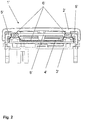
- Fig. 1 and 2 show a prior art switch 1 '.
- the switch 1 'for producing or interrupting a current flow by manually operating a rocker switch 2' comprises a base 3 ', a circuit board 4' and the rocker switch 2 ', with an inner cover 5' between the rocker switch 2 'and the circuit board 4' is arranged and wherein the inner cover 5 'is assigned at least one elastic buffer element to rest on the rocker switch 2'.
- the elastic buffer element is designed as a silicone part 6 '.
- the silicone part 6 'and the inner cover 5' consist of different materials.
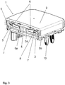
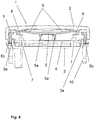
- Fig. 3 and 4th show an electrical switch 1 for producing or interrupting an electrical current flow by manually operating a rocker switch 2, comprising a base 3, a printed circuit board 4, which is designed as a PCB ("Printed Circuit Board”; in German: printed circuit board or flat assembly) , and the rocker switch 2.
- a rocker switch 2 comprising a base 3, a printed circuit board 4, which is designed as a PCB ("Printed Circuit Board"; in German: printed circuit board or flat assembly) , and the rocker switch 2.
- An inner cover 5 is arranged between the rocker switch 2 and the printed circuit board 4, the inner cover 5 being assigned a plurality of elastic buffer elements for contact with the rocker switch 2.
- the buffer elements are designed as integral components of the inner cover 5.
- the buffer elements are made of the same material and are designed in one piece with the inner cover 5.
- the buffer elements act as actuators with stop elements 7 on the circuit board 4 and come to rest on the rocker switch 2 when it is actuated.
- the buffer elements are designed as spring tongues 6, each with one end directly or indirectly resiliently resting against the rocker switch 2 and are each fixed with their other end on the inner cover 5.
- Fig. 3 and 4th show that each spring tongue 6 is arched, preformed or pretensioned in the axial direction, so that it rests with its free end on the interior of the rocker switch 2.
- Fig. 4 shows particularly clearly that each spring tongue 6 is turned inward at its free end facing the rocker switch 2, namely in the direction of the printed circuit board 4, and has a U- or V-shaped bead 8.
- Fig. 3 and 4th also show that the inner cover 5 rests on the circuit board 4 with at least one support web 5a or a web structure, a spring tongue 6 protruding from the at least one support web 5a or the web structure and being connected to it.
- Fig. 5 shows in an exploded view of the switch 1 according to Fig. 3 and 4th that four buffer elements, namely four spring tongues 6 are provided, which are formed in corner areas of the inner cover 5.
- the inner cover 5 is essentially square in a plan view in the direction of the printed circuit board 4 and has rounded corners.
- the stop elements 7 or switching contacts for the contact of the spring tongues 6 are arranged in the corner areas thereof.
- the only components of the switch 1 are the base 3, the printed circuit board 4, the rocker switch 2 and the inner cover 5.
- the circuit board 4 is designed as a PCB.
- Fig. 5 and 6th show that in a central area of the inner cover 5, namely laterally within the four buffer elements, two tabs 9 are provided, which are made of the same material and in one piece with the inner cover 5 and which protrude with angled edges 9a in the direction of the rocker switch 2.
- the tabs 9 protrude with their free ends, which the angled edges 9a wear, in the opposite direction from a center of the inner cover 5 in the lateral direction.
- the inner cover 5 is sandwiched between the base 3 and the rocker switch 2 and overlaps the base 3 with a side wall 5b at least in sections at an edge 3a of the base 3.
- the inner cover 5 acts as a kind of hood and chambers the circuit board 4 between yourself and the base 3.
- Fig. 5 shows that latching tongues 3b protrude from the base 3 in the direction of the rocker switch 2, which counter-elements 5c of the inner cover 5 can engage behind and thus lock the inner cover 5 to the base 3.
- the counter elements 5c are designed as strip-like structures and in Fig. 7 shown in the bottom view.
Landscapes
- Switch Cases, Indication, And Locking (AREA)
- Tumbler Switches (AREA)
- Push-Button Switches (AREA)
Abstract
Description
- Die Erfindung betrifft einen Schalter zum Herstellen oder Unterbrechen eines Stromflusses durch das händische Betätigen einer Schaltwippe, umfassend einen Sockel, eine Leiterplatte und eine Schaltwippe, wobei zwischen der Schaltwippe und der Leiterplatte eine innere Abdeckung angeordnet ist und wobei der inneren Abdeckung mindestens ein elastisches Pufferelement zur Anlage an der Schaltwippe zugeordnet ist.
- In vielen Produkten, insbesondere in Schaltern, werden als Pufferelemente Silikonteile verwendet, um Raum zwischen einem mechanischen Stellorgan, insbesondere einer Schaltwippe, und einem End- oder Mikroschalter auszufüllen.
- Diese Silikonteile erfüllen verschiedene Funktionen, wie beispielsweise das Kontrollieren einer Haptik durch die Dicke des Silikonmaterials oder das Schützen des End- oder Mikroschalters und einer Leiterplatte vor überhöhten Belastungen durch die Steifheit des Silikonmaterials.
- Silikonteile erhöhen jedoch den Aufwand bei der Fertigung eines Schalters. Insbesondere müssen solche Silikonteile in aufwendiger Weise auf Lager gehalten und verbaut werden. Des Weiteren können Silikonteile nach längerer Zeit unter sehr ungünstigen Umständen spröde und/ oder rissig werden
Der Erfindung liegt daher die Aufgabe zugrunde, einen Schalter zu realisieren, dessen Leiterplatte bei möglichst teilearmem Aufbau vor mechanischen Belastungen durch die Schaltwippe möglichst lange geschützt ist und/ oder dessen Haptik bei möglichst teilearmem Aufbau kontrolliert werden kann. - Erfindungsgemäß wird die voranstehende Aufgabe durch einen Schalter mit den Merkmalen des Anspruchs 1 gelöst. Danach ist der eingangs genannte Schalter dadurch gekennzeichnet, dass ein Pufferelement oder mehrere Pufferelemente als integraler Bestandteil oder als integrale Bestandteile der inneren Abdeckung ausgestaltet ist oder sind.
- Erfindungsgemäß ist erkannt worden, dass lediglich die Funktionen eines zusätzlichen Silikonteils, nicht jedoch dieses selbst, in ein Bauteil integriert werden müssen. So kann das Silikonteil erfindungsgemäß eingespart werden. Erfindungsgemäß wird die Pufferfunktion durch ein ohnehin notwendiges oder bestehendes Bauteil, wie hier konkret durch die innere Abdeckung, erfüllt. Durch die Pufferfunktion werden die Haptik und der Schutz elektrischer Komponenten optimiert. Konkret ist die Haptik der Schaltwippenbetätigung durch einen teilearmen Aufbau optimiert und ist der Schutz der Leiterplatte durch einen teilearmen Aufbau optimiert. Der Schalter weist insgesamt einen teilearmen Aufbau auf, weil kein Silikonteil mehr in die innere Abdeckung integriert ist. Überraschend wirkt ein solches integriertes Pufferelement aber wie ein Silikonteil.
- Vorteilhaft ist das Pufferelement materialeinheitlich und einstückig mit der inneren Abdeckung ausgestaltet. Alternativ oder zusätzlich ist die innere Abdeckung einteilig als ein einziges zusammenhängendes Bauteil ausgestaltet. Hierdurch kann das Pufferelement aus einem relativ steifen und dennoch flexiblen aber dauerhaft haltbaren Material, wie insbesondere einem Hartkunststoff, gefertigt werden. Des Weiteren können Kosten eingespart werden, weil nur noch ein Bauteil zur Herstellung der inneren Abdeckung gefertigt werden muss.
- Weiter vorteilhaft wirkt das Pufferelement als Betätigungsorgan mit einem Anschlagelement auf der Leiterplatte zusammen und/ oder kommt an diesem zur Anlage. So fungiert das Pufferelement zugleich als Betätigungsorgan. Das Anschlagelement ist bevorzugt als elektrischer Schaltkontakt ausgestaltet.
- Vorteilhaft ist das Pufferelement als Federzunge ausgebildet, welche mit einem Ende mittelbar oder unmittelbar federnd an der Schaltwippe anliegt oder an dieser federnd anlegbar ist und mit ihrem anderen Ende an der inneren Abdeckung festgelegt ist. Federzungen können problemlos Elemente eines bereits bestehenden Bauteils, nämlich der inneren Abdeckung, sein. Bevorzugt sind die Federzungen Elemente einer Gehäusestruktur. Die Federzungen können einen hinreichend steifen Aufbau zeigen. Durch diesen Aufbau ist eine Federzunge ein flexibles Betätigungsorgan. Aufgrund der flexiblen Eigenschaften dieses Betätigungsorgans wirkt dieses wie ein Silikonteil und bietet einen Schutz für eine Leiterplatte. Außerdem bietet es viele Möglichkeiten, die Haptik der Schaltwippenbetätigung zu optimieren.
- Weiter vorteilhaft ist die Federzunge in axialer Richtung vorgewölbt, vorgeformt oder vorgespannt, so dass sie mit ihrem Ende an der Schaltwippe anliegt oder an dieser federnd anlegbar ist. So kann eine Rückstellkraft auf die Schaltwippe ausgeübt werden und/ oder es kann Bewegungsenergie, die in die Schaltwippe eingetragen wird, zumindest teilweise absorbiert werden. Die Bewegung und/ oder das Anschlagverhalten der Schaltwippe kann bzw. können gedämpft werden.
- Vorteilhaft ist die Federzunge an ihrem der Schaltwippe zugewandten Ende nach innen, nämlich in Richtung der Leiterplatte, umgeschlagen. Alternativ oder zusätzlich weist diese einen U- oder V-förmigen Wulst auf. Durch das Umschlagen in Richtung der Leiterplatte können dort Anschlagelemente oder Schaltkontakte leichter erreicht werden. Ein Wulst erhöht die Dicke der Federzunge an ihrem Ende, so dass dieses effektiv und zuverlässig auf die Anschlagelemente oder Schaltkontakte einwirken kann.
- Weiter vorteilhaft ruht die innere Abdeckung mit mindestens einem Stützsteg oder einer Stegstruktur auf der Leiterplatte, wobei die Federzunge von dem mindestens einen Stützsteg oder der Stegstruktur bevorzugt in lateraler Richtung abragt und an diesen bzw. diese angebunden ist. Ein Steg oder eine Stegstruktur erhöht bzw. erhöhen die Steifigkeit der inneren Abdeckung. Des Weiteren ist ein Steg ein relativ filigranes Stützelement, welches die Leiterplatte nur wenig belastet.
- Vorteilhaft sind vier Pufferelemente vorgesehen, welche in Eckbereichen der inneren Abdeckung ausgebildet sind. Die innere Abdeckung ist in Draufsicht bevorzugt als im Wesentlichen rechteckiges oder quadratisches Bauteil mit abgerundeten Ecken ausgebildet. Durch vier Pufferelemente wird die Schaltwippe besonders effektiv federnd gelagert und/ oder federnd abgestützt.
- Weiter vorteilhaft sind in einem Zentralbereich der inneren Abdeckung, nämlich lateral innerhalb der vier Pufferelemente oder im Wesentlichen mittig, zwei Laschen vorgesehen, welche materialeinheitlich und einstückig mit der inneren Abdeckung ausgebildet sind und welche mit abgewinkelten Rändern in Richtung der Schaltwippe abragen. Die Laschen können ebenfalls eine Federwirkung entfalten und die Schaltwippe federnd lagern oder abstützen. Die Laschen sind insoweit innen liegende Federlager.
- Vorteilhaft ist die innere Abdeckung sandwichartig zwischen dem Sockel und der Schaltwippe angeordnet und übergreift dabei den Sockel mit einer Seitenwand zumindest abschnittsweise an einem Rand des Sockels. Hierdurch ist ein Verrücken der inneren Abdeckung relativ zum Sockel in lateraler Richtung unterbunden. Die innere Abdeckung ist vorteilhaft als eine Art Haube ausgebildet, welche die Leiterplatte zwischen sich und dem Sockel kammert.
- Weiter vorteilhaft ragen vom Sockel Rastzungen in Richtung der Schaltwippe ab, welche Gegenelemente der inneren Abdeckung hintergreifen und so die innere Abdeckung mit dem Sockel verrasten. Hierdurch kann die innere Abdeckung die Leiterplatte, die auf dem Sockel aufliegt, verliersicher abdecken.
- Bevorzugt ist die innere Abdeckung aus einem Kunststoff gefertigt, insbesondere aus einem Hartkunststoff, der härter und biegesteifer ist als Silikon. Ein solcher Kunststoff kann spritzgusstechnisch verarbeitet werden.
- In der Zeichnung zeigen
- Fig. 1
- eine perspektivische, teilweise geschnittene Ansicht eines Schalters gemäß dem Stand der Technik, bei welchem einer inneren Abdeckung ein Silikonteil als zusätzliches Bauteil zugeordnet ist,
- Fig. 2
- eine Schnittansicht des Schalters gemäß
Fig. 1 , bei welchem einer inneren Abdeckung ein Silikonteil als zusätzliches Bauteil zugeordnet ist, wobei das Silikonteil in die innere Abdeckung integriert ist, - Fig. 3
- eine perspektivische, teilweise geschnittene Ansicht eines Schalters in zusammen gebautem Zustand, bei welchem einer inneren Abdeckung Pufferelemente als integrale Bestandteile zugeordnet sind,
- Fig. 4
- eine Schnittansicht des Schalters gemäß
Fig. 3 , bei welchem einer inneren Abdeckung Pufferelemente als integrale, materialeinheitliche Bestandteile zugeordnet sind, - Fig. 5
- eine perspektivische Explosionsansicht des Schalters gemäß
Fig. 3 , welche darstellt, dass die innere Abdeckung als zusammenhängendes einstückiges Bauteil ausgebildet ist, - Fig. 6
- oben eine teilweise geschnittene Ansicht des Schalters gemäß
Fig. 3 , wobei die als Federzungen ausgestalteten Pufferelemente von oben dargestellt sind, und unten den Schalter gemäßFig. 3 ohne Schaltwippe, und - Fig. 7
- oben eine Draufsicht auf die Fläche der inneren Abdeckung, welche im zusammen gebauten Zustand des Schalters der Schaltwippe zugewandt ist, und unten eine perspektivische Ansicht der Innenstrukturen der inneren Abdeckung, welche im zusammengebauten Zustand des Schalters der Leiterplatte zugewandt sind.
-
Fig. 1 und2 zeigen einen Schalter 1' des Stands der Technik. Der Schalter 1' zum Herstellen oder Unterbrechen eines Stromflusses durch das händische Betätigen einer Schaltwippe 2' umfasst einen Sockel 3', eine Leiterplatte 4' und die Schaltwippe 2', wobei zwischen der Schaltwippe 2' und der Leiterplatte 4' eine innere Abdeckung 5' angeordnet ist und wobei der inneren Abdeckung 5' mindestens ein elastisches Pufferelement zur Anlage an der Schaltwippe 2' zugeordnet ist. Das elastische Pufferelement ist als Silikonteil 6' ausgestaltet. Das Silikonteil 6' und die innere Abdeckung 5' bestehen aus unterschiedlichen Materialien. -
Fig. 3 und4 zeigen einen elektrischen Schalter 1 zum Herstellen oder Unterbrechen eines elektrischen Stromflusses durch das händische Betätigen einer Schaltwippe 2, umfassend einen Sockel 3, eine Leiterplatte 4, welche als PCB ("Printed Circuit Board"; in deutscher Sprache: gedruckte Leiterplatte oder Flachbaugruppe) ausgestaltet ist, und die Schaltwippe 2. - Zwischen der Schaltwippe 2 und der Leiterplatte 4 ist eine innere Abdeckung 5 angeordnet, wobei der inneren Abdeckung 5 mehrere elastische Pufferelemente zur Anlage an der Schaltwippe 2 zugeordnet sind. Die Pufferelemente sind als integrale Bestandteile der inneren Abdeckung 5 ausgestaltet.
- Die Pufferelemente sind materialeinheitlich und einstückig mit der inneren Abdeckung 5 ausgestaltet. Die Pufferelemente wirken als Betätigungsorgane mit Anschlagelementen 7 auf der Leiterplatte 4 zusammen und kommen beim Betätigen der Schaltwippe 2 an diesen zur Anlage.
- Konkret sind die Pufferelemente als Federzungen 6 ausgebildet, welche jeweils mit einem Ende mittelbar oder unmittelbar federnd an der Schaltwippe 2 anliegen und jeweils mit ihrem anderen Ende an der inneren Abdeckung 5 festgelegt sind.
-
Fig. 3 und4 zeigen, dass jede Federzunge 6 in axialer Richtung vorgewölbt, vorgeformt oder vorgespannt ist, so dass sie mit ihrem freien Ende am Inneren der Schaltwippe 2 anliegt.Fig. 4 zeigt besonders deutlich, dass jede Federzunge 6 an ihrem der Schaltwippe 2 zugewandten freien Ende nach innen, nämlich in Richtung der Leiterplatte 4, umgeschlagen ist und einen U- oder V-förmigen Wulst 8 aufweist. -
Fig. 3 und4 zeigen auch, dass die innere Abdeckung 5 mit mindestens einem Stützsteg 5a oder einer Stegstruktur auf der Leiterplatte 4 ruht, wobei eine Federzunge 6 von dem mindestens einen Stützsteg 5a oder der Stegstruktur abragt und an diesen bzw. diese angebunden ist. -
Fig. 5 zeigt in einer Explosionsansicht des Schalters 1 gemäßFig. 3 und4 , dass vier Pufferelemente, nämlich vier Federzungen 6 vorgesehen sind, welche in Eckbereichen der inneren Abdeckung 5 ausgebildet sind. Die innere Abdeckung 5 ist in einer Draufsicht in Richtung der Leiterplatte 4 im Wesentlichen quadratisch ausgebildet und weist abgerundete Ecken auf. - Auf der Leiterplatte 4 sind in deren Eckbereichen die Anschlagelemente 7 oder Schaltkontakte für die Anlage der Federzungen 6 angeordnet.
- Der Schalter 1 weist als wesentliche Komponenten nur den Sockel 3, die Leiterplatte 4, die Schaltwippe 2 und die innere Abdeckung 5 auf. Die Leiterplatte 4 ist als PCB ausgestaltet.
-
Fig. 5 und6 zeigen, dass in einem Zentralbereich der inneren Abdeckung 5, nämlich lateral innerhalb der vier Pufferelemente, zwei Laschen 9 vorgesehen sind, welche materialeinheitlich und einstückig mit der inneren Abdeckung 5 ausgebildet sind und welche mit abgewinkelten Rändern 9a in Richtung der Schaltwippe 2 abragen. Die Laschen 9 ragen dabei mit ihren freien Enden, welche die abgewinkelten Ränder 9a tragen, in entgegengesetzter Richtung von einem Zentrum der inneren Abdeckung 5 in lateraler Richtung ab. - Die innere Abdeckung 5 ist sandwichartig zwischen dem Sockel 3 und der Schaltwippe 2 angeordnet und übergreift dabei den Sockel 3 mit einer Seitenwand 5b zumindest abschnittsweise an einem Rand 3a des Sockels 3. Die innere Abdeckung 5 wirkt als eine Art Haube und kammert die Leiterplatte 4 zwischen sich und dem Sockel 3.
-
Fig. 5 zeigt, dass vom Sockel 3 Rastzungen 3b in Richtung der Schaltwippe 2 abragen, welche Gegenelemente 5c der inneren Abdeckung 5 hintergreifen können und so die innere Abdeckung 5 mit dem Sockel 3 verrasten. Die Gegenelemente 5c sind als leistenartige Strukturen ausgebildet und inFig. 7 in der unteren Ansicht dargestellt.Bezugszeichenliste 1, 1' Schalter 2, 2' Schaltwippe 3, 3' Sockel 3a Rand von 3 3b Rastzunge von 3 4, 4' Leiterplatte oder PCB 5, 5' Innere Abdeckung 5a Steg von 5 5b Seitenwand von 5 5c Gegenelement von 5 6 Federzunge von 5 6' Silikonteil von 1' 7 Anschlagelement oder Kontakt von 4 8 Wulst von 6 9 Laschen von 5 9a Rand von 9 10 Montagefeder von 3
Claims (11)
- Schalter (1) zum Herstellen oder Unterbrechen eines Stromflusses durch das händische Betätigen einer Schaltwippe (2), umfassend einen Sockel (3), eine Leiterplatte (4) und eine Schaltwippe (2), wobei zwischen der Schaltwippe (2) und der Leiterplatte (4) eine innere Abdeckung (5) angeordnet ist und wobei der inneren Abdeckung (5) mindestens ein elastisches Pufferelement zur Anlage an der Schaltwippe (2) zugeordnet ist,
dadurch gekennzeichnet, dass ein Pufferelement oder mehrere Pufferelemente als integraler Bestandteil oder als integrale Bestandteile der inneren Abdeckung (5) ausgestaltet ist oder sind. - Schalter nach Anspruch 1, dadurch gekennzeichnet, dass das Pufferelement materialeinheitlich und einstückig mit der inneren Abdeckung (5) ausgestaltet ist und/ oder dass die innere Abdeckung (5) einteilig als ein einziges zusammenhängendes Bauteil ausgestaltet ist.
- Schalter nach Anspruch 1 oder 2, dadurch gekennzeichnet, dass das Pufferelement als Betätigungsorgan mit einem Anschlagelement (7) auf der Leiterplatte (4) zusammenwirkt und/ oder an diesem zur Anlage kommt.
- Schalter nach einem der Ansprüche 1 bis 3, dadurch gekennzeichnet, dass das Pufferelement als Federzunge (6) ausgebildet ist, welche mit einem Ende mittelbar oder unmittelbar federnd an der Schaltwippe (2) anliegt oder an dieser federnd anlegbar ist und mit ihrem anderen Ende an der inneren Abdeckung (5) festgelegt ist.
- Schalter nach Anspruch 4, dadurch gekennzeichnet, dass die Federzunge (6) in axialer Richtung vorgewölbt, vorgeformt oder vorgespannt ist, so dass sie mit ihrem Ende an der Schaltwippe (2) anliegt oder an dieser federnd anlegbar ist.
- Schalter nach Anspruch 4 oder 5, dadurch gekennzeichnet, dass die Federzunge (6) an ihrem der Schaltwippe (2) zugewandten Ende nach innen, nämlich in Richtung der Leiterplatte (4), umgeschlagen ist und/ oder einen U- oder V-förmigen Wulst (8) aufweist.
- Schalter nach einem der Ansprüche 4 bis 6, dadurch gekennzeichnet, dass die innere Abdeckung (5) mit mindestens einem Stützsteg (5a) oder einer Stegstruktur auf der Leiterplatte (4) ruht, wobei die Federzunge (6) von dem mindestens einen Stützsteg (5a) oder der Stegstruktur abragt und an diesen bzw. diese angebunden ist.
- Schalter nach einem der voranstehenden Ansprüche, dadurch gekennzeichnet, dass vier Pufferelemente vorgesehen sind, welche in Eckbereichen der inneren Abdeckung (5) ausgebildet sind.
- Schalter nach Anspruch 8, dadurch gekennzeichnet, dass in einem Zentralbereich der inneren Abdeckung (5), nämlich lateral innerhalb der vier Pufferelemente, zwei Laschen (9) vorgesehen sind, welche materialeinheitlich und einstückig mit der inneren Abdeckung (5) ausgebildet sind und welche mit abgewinkelten Rändern (9a) in Richtung der Schaltwippe (2) abragen.
- Schalter nach einem der voranstehenden Ansprüche, dadurch gekennzeichnet, dass die innere Abdeckung (5) sandwichartig zwischen dem Sockel (3) und der Schaltwippe (2) angeordnet ist und dabei den Sockel (3) mit mindestens einer Seitenwand (5b) zumindest abschnittsweise an einem Rand (3a) des Sockels übergreift.
- Schalter nach einem der voranstehenden Ansprüche, dadurch gekennzeichnet, dass vom Sockel (3) Rastzungen (3b) in Richtung der Schaltwippe (2) abragen, welche Gegenelemente (5c) der inneren Abdeckung (5) hintergreifen und so die innere Abdeckung (5) mit dem Sockel (3) verrasten.
Applications Claiming Priority (1)
| Application Number | Priority Date | Filing Date | Title |
|---|---|---|---|
| DE102019130772.4A DE102019130772A1 (de) | 2019-11-14 | 2019-11-14 | Schalter mit einer Schaltwippe |
Publications (2)
| Publication Number | Publication Date |
|---|---|
| EP3823000A1 true EP3823000A1 (de) | 2021-05-19 |
| EP3823000B1 EP3823000B1 (de) | 2023-04-12 |
Family
ID=73059520
Family Applications (1)
| Application Number | Title | Priority Date | Filing Date |
|---|---|---|---|
| EP20205362.5A Active EP3823000B1 (de) | 2019-11-14 | 2020-11-03 | Schalter mit einer schaltwippe |
Country Status (2)
| Country | Link |
|---|---|
| EP (1) | EP3823000B1 (de) |
| DE (1) | DE102019130772A1 (de) |
Cited By (1)
| Publication number | Priority date | Publication date | Assignee | Title |
|---|---|---|---|---|
| EP4542608A4 (de) * | 2022-07-07 | 2026-03-04 | Wuhan Linptech Co Ltd | Intelligenter wandschalter, drahtloser intelligenter schalter und schaltermontagegestell |
Families Citing this family (1)
| Publication number | Priority date | Publication date | Assignee | Title |
|---|---|---|---|---|
| FR3159282B1 (fr) * | 2024-02-13 | 2026-01-02 | Somfy Activites Sa | Dispositif de commande pour commander un équipement domotique |
Citations (4)
| Publication number | Priority date | Publication date | Assignee | Title |
|---|---|---|---|---|
| US4401864A (en) * | 1980-07-10 | 1983-08-30 | Olympus Optical Company Ltd. | Seesaw type switch mechanism |
| DE102008015129B3 (de) * | 2008-03-20 | 2009-07-23 | Abb Ag | Unterputz-Schalter mit mindestens einer innerhalb eines Abdeckrahmens angeordneten Betätigungswippe |
| DE202008015469U1 (de) * | 2008-11-21 | 2010-04-22 | Eldat Gmbh | Gehäuse für einen Schalter sowie Schalter |
| DE202011109300U1 (de) * | 2011-12-20 | 2013-03-21 | Eldat Gmbh | Hygrostat |
Family Cites Families (3)
| Publication number | Priority date | Publication date | Assignee | Title |
|---|---|---|---|---|
| DE19627294A1 (de) * | 1996-07-06 | 1998-01-08 | Abb Patent Gmbh | Wipptaster |
| DE202004005837U1 (de) * | 2004-04-14 | 2004-07-08 | Enocean Gmbh | Schaltergehäuse zur Aufputzmontage und zur Aufnahme eines elektronischen Moduls |
| DE102016104271A1 (de) * | 2016-03-09 | 2017-09-14 | Schneider Electric Industries Sas | Installationsgerät |
-
2019
- 2019-11-14 DE DE102019130772.4A patent/DE102019130772A1/de not_active Withdrawn
-
2020
- 2020-11-03 EP EP20205362.5A patent/EP3823000B1/de active Active
Patent Citations (4)
| Publication number | Priority date | Publication date | Assignee | Title |
|---|---|---|---|---|
| US4401864A (en) * | 1980-07-10 | 1983-08-30 | Olympus Optical Company Ltd. | Seesaw type switch mechanism |
| DE102008015129B3 (de) * | 2008-03-20 | 2009-07-23 | Abb Ag | Unterputz-Schalter mit mindestens einer innerhalb eines Abdeckrahmens angeordneten Betätigungswippe |
| DE202008015469U1 (de) * | 2008-11-21 | 2010-04-22 | Eldat Gmbh | Gehäuse für einen Schalter sowie Schalter |
| DE202011109300U1 (de) * | 2011-12-20 | 2013-03-21 | Eldat Gmbh | Hygrostat |
Cited By (1)
| Publication number | Priority date | Publication date | Assignee | Title |
|---|---|---|---|---|
| EP4542608A4 (de) * | 2022-07-07 | 2026-03-04 | Wuhan Linptech Co Ltd | Intelligenter wandschalter, drahtloser intelligenter schalter und schaltermontagegestell |
Also Published As
| Publication number | Publication date |
|---|---|
| EP3823000B1 (de) | 2023-04-12 |
| DE102019130772A1 (de) | 2021-05-20 |
Similar Documents
| Publication | Publication Date | Title |
|---|---|---|
| DE60007537T2 (de) | Verbesserter elektroschalter mit fühlbarem effekt und einen einzigen schaltglied | |
| DE4030030C2 (de) | Tastenschalter | |
| EP2450228A2 (de) | Fahrzeugsitz | |
| EP3823000B1 (de) | Schalter mit einer schaltwippe | |
| EP2290672B1 (de) | Kontaktanordnung für elektromechanische Hilfsschalter | |
| EP2633537B1 (de) | Schlüsselkartenschalter | |
| DE102006031584B4 (de) | Miniaturisierter elektrischer Schalter | |
| EP3021439A2 (de) | Elektronisches installationsgerät | |
| EP1411285A1 (de) | Piezoelektrisches Ventil | |
| DE2705756C2 (de) | Druckknopfschalter für elektronische Tischrechner o.dgl. | |
| DE2926683C2 (de) | Gabelumschalter für Fernsprechapparate | |
| DE202015102661U1 (de) | Gefederter Taster | |
| EP3686909A1 (de) | Elektroinstallationsgerät mit sockelaufsatz | |
| CH450521A (de) | Kippwerk, insbesondere für eine Schaltvorrichtung | |
| EP1482527A1 (de) | Tastenblock | |
| DE29615428U1 (de) | Notaus-Schalter | |
| DE2004787A1 (de) | Elektrischer Schalter | |
| DE4442312C2 (de) | Schalterbaugruppe | |
| DE2404906A1 (de) | Elektrischer schalter | |
| DD270404B5 (de) | Tastenfeld fuer schreib- und computertechnik | |
| DE102012110130B3 (de) | Elektrisches Installationsgerät | |
| DE1152462B (de) | Anbaufaehiges Vorsatzgeraet fuer elektrische Drucktaster | |
| DE2936156C2 (de) | Stößelrelais für Wasch- oder Geschirrspülmaschinen | |
| DE19816946C1 (de) | Schnappscheibenschalter | |
| DE1300604B (de) | Selbstrueckstellender elektrischer Schnappschalter |
Legal Events
| Date | Code | Title | Description |
|---|---|---|---|
| PUAI | Public reference made under article 153(3) epc to a published international application that has entered the european phase |
Free format text: ORIGINAL CODE: 0009012 |
|
| STAA | Information on the status of an ep patent application or granted ep patent |
Free format text: STATUS: THE APPLICATION HAS BEEN PUBLISHED |
|
| AK | Designated contracting states |
Kind code of ref document: A1 Designated state(s): AL AT BE BG CH CY CZ DE DK EE ES FI FR GB GR HR HU IE IS IT LI LT LU LV MC MK MT NL NO PL PT RO RS SE SI SK SM TR |
|
| STAA | Information on the status of an ep patent application or granted ep patent |
Free format text: STATUS: REQUEST FOR EXAMINATION WAS MADE |
|
| 17P | Request for examination filed |
Effective date: 20210903 |
|
| RBV | Designated contracting states (corrected) |
Designated state(s): AL AT BE BG CH CY CZ DE DK EE ES FI FR GB GR HR HU IE IS IT LI LT LU LV MC MK MT NL NO PL PT RO RS SE SI SK SM TR |
|
| RIC1 | Information provided on ipc code assigned before grant |
Ipc: H01H 9/02 20060101ALN20221215BHEP Ipc: H01H 23/16 20060101ALN20221215BHEP Ipc: H01H 23/14 20060101ALN20221215BHEP Ipc: H01H 23/30 20060101ALI20221215BHEP Ipc: H01H 21/24 20060101AFI20221215BHEP |
|
| GRAP | Despatch of communication of intention to grant a patent |
Free format text: ORIGINAL CODE: EPIDOSNIGR1 |
|
| STAA | Information on the status of an ep patent application or granted ep patent |
Free format text: STATUS: GRANT OF PATENT IS INTENDED |
|
| GRAS | Grant fee paid |
Free format text: ORIGINAL CODE: EPIDOSNIGR3 |
|
| INTG | Intention to grant announced |
Effective date: 20230130 |
|
| GRAA | (expected) grant |
Free format text: ORIGINAL CODE: 0009210 |
|
| STAA | Information on the status of an ep patent application or granted ep patent |
Free format text: STATUS: THE PATENT HAS BEEN GRANTED |
|
| AK | Designated contracting states |
Kind code of ref document: B1 Designated state(s): AL AT BE BG CH CY CZ DE DK EE ES FI FR GB GR HR HU IE IS IT LI LT LU LV MC MK MT NL NO PL PT RO RS SE SI SK SM TR |
|
| REG | Reference to a national code |
Ref country code: GB Ref legal event code: FG4D Free format text: NOT ENGLISH |
|
| REG | Reference to a national code |
Ref country code: CH Ref legal event code: EP |
|
| REG | Reference to a national code |
Ref country code: DE Ref legal event code: R096 Ref document number: 502020002968 Country of ref document: DE |
|
| REG | Reference to a national code |
Ref country code: IE Ref legal event code: FG4D Free format text: LANGUAGE OF EP DOCUMENT: GERMAN |
|
| REG | Reference to a national code |
Ref country code: AT Ref legal event code: REF Ref document number: 1560250 Country of ref document: AT Kind code of ref document: T Effective date: 20230515 |
|
| REG | Reference to a national code |
Ref country code: NL Ref legal event code: FP |
|
| REG | Reference to a national code |
Ref country code: LT Ref legal event code: MG9D |
|
| PG25 | Lapsed in a contracting state [announced via postgrant information from national office to epo] |
Ref country code: SE Free format text: LAPSE BECAUSE OF FAILURE TO SUBMIT A TRANSLATION OF THE DESCRIPTION OR TO PAY THE FEE WITHIN THE PRESCRIBED TIME-LIMIT Effective date: 20230412 Ref country code: PT Free format text: LAPSE BECAUSE OF FAILURE TO SUBMIT A TRANSLATION OF THE DESCRIPTION OR TO PAY THE FEE WITHIN THE PRESCRIBED TIME-LIMIT Effective date: 20230814 Ref country code: NO Free format text: LAPSE BECAUSE OF FAILURE TO SUBMIT A TRANSLATION OF THE DESCRIPTION OR TO PAY THE FEE WITHIN THE PRESCRIBED TIME-LIMIT Effective date: 20230712 Ref country code: ES Free format text: LAPSE BECAUSE OF FAILURE TO SUBMIT A TRANSLATION OF THE DESCRIPTION OR TO PAY THE FEE WITHIN THE PRESCRIBED TIME-LIMIT Effective date: 20230412 |
|
| PG25 | Lapsed in a contracting state [announced via postgrant information from national office to epo] |
Ref country code: RS Free format text: LAPSE BECAUSE OF FAILURE TO SUBMIT A TRANSLATION OF THE DESCRIPTION OR TO PAY THE FEE WITHIN THE PRESCRIBED TIME-LIMIT Effective date: 20230412 Ref country code: PL Free format text: LAPSE BECAUSE OF FAILURE TO SUBMIT A TRANSLATION OF THE DESCRIPTION OR TO PAY THE FEE WITHIN THE PRESCRIBED TIME-LIMIT Effective date: 20230412 Ref country code: LV Free format text: LAPSE BECAUSE OF FAILURE TO SUBMIT A TRANSLATION OF THE DESCRIPTION OR TO PAY THE FEE WITHIN THE PRESCRIBED TIME-LIMIT Effective date: 20230412 Ref country code: LT Free format text: LAPSE BECAUSE OF FAILURE TO SUBMIT A TRANSLATION OF THE DESCRIPTION OR TO PAY THE FEE WITHIN THE PRESCRIBED TIME-LIMIT Effective date: 20230412 Ref country code: IS Free format text: LAPSE BECAUSE OF FAILURE TO SUBMIT A TRANSLATION OF THE DESCRIPTION OR TO PAY THE FEE WITHIN THE PRESCRIBED TIME-LIMIT Effective date: 20230812 Ref country code: HR Free format text: LAPSE BECAUSE OF FAILURE TO SUBMIT A TRANSLATION OF THE DESCRIPTION OR TO PAY THE FEE WITHIN THE PRESCRIBED TIME-LIMIT Effective date: 20230412 Ref country code: GR Free format text: LAPSE BECAUSE OF FAILURE TO SUBMIT A TRANSLATION OF THE DESCRIPTION OR TO PAY THE FEE WITHIN THE PRESCRIBED TIME-LIMIT Effective date: 20230713 |
|
| PG25 | Lapsed in a contracting state [announced via postgrant information from national office to epo] |
Ref country code: FI Free format text: LAPSE BECAUSE OF FAILURE TO SUBMIT A TRANSLATION OF THE DESCRIPTION OR TO PAY THE FEE WITHIN THE PRESCRIBED TIME-LIMIT Effective date: 20230412 |
|
| REG | Reference to a national code |
Ref country code: DE Ref legal event code: R097 Ref document number: 502020002968 Country of ref document: DE |
|
| PG25 | Lapsed in a contracting state [announced via postgrant information from national office to epo] |
Ref country code: SK Free format text: LAPSE BECAUSE OF FAILURE TO SUBMIT A TRANSLATION OF THE DESCRIPTION OR TO PAY THE FEE WITHIN THE PRESCRIBED TIME-LIMIT Effective date: 20230412 |
|
| PG25 | Lapsed in a contracting state [announced via postgrant information from national office to epo] |
Ref country code: SM Free format text: LAPSE BECAUSE OF FAILURE TO SUBMIT A TRANSLATION OF THE DESCRIPTION OR TO PAY THE FEE WITHIN THE PRESCRIBED TIME-LIMIT Effective date: 20230412 Ref country code: SK Free format text: LAPSE BECAUSE OF FAILURE TO SUBMIT A TRANSLATION OF THE DESCRIPTION OR TO PAY THE FEE WITHIN THE PRESCRIBED TIME-LIMIT Effective date: 20230412 Ref country code: RO Free format text: LAPSE BECAUSE OF FAILURE TO SUBMIT A TRANSLATION OF THE DESCRIPTION OR TO PAY THE FEE WITHIN THE PRESCRIBED TIME-LIMIT Effective date: 20230412 Ref country code: EE Free format text: LAPSE BECAUSE OF FAILURE TO SUBMIT A TRANSLATION OF THE DESCRIPTION OR TO PAY THE FEE WITHIN THE PRESCRIBED TIME-LIMIT Effective date: 20230412 Ref country code: DK Free format text: LAPSE BECAUSE OF FAILURE TO SUBMIT A TRANSLATION OF THE DESCRIPTION OR TO PAY THE FEE WITHIN THE PRESCRIBED TIME-LIMIT Effective date: 20230412 |
|
| PLBE | No opposition filed within time limit |
Free format text: ORIGINAL CODE: 0009261 |
|
| STAA | Information on the status of an ep patent application or granted ep patent |
Free format text: STATUS: NO OPPOSITION FILED WITHIN TIME LIMIT |
|
| 26N | No opposition filed |
Effective date: 20240115 |
|
| PG25 | Lapsed in a contracting state [announced via postgrant information from national office to epo] |
Ref country code: SI Free format text: LAPSE BECAUSE OF FAILURE TO SUBMIT A TRANSLATION OF THE DESCRIPTION OR TO PAY THE FEE WITHIN THE PRESCRIBED TIME-LIMIT Effective date: 20230412 |
|
| PG25 | Lapsed in a contracting state [announced via postgrant information from national office to epo] |
Ref country code: SI Free format text: LAPSE BECAUSE OF FAILURE TO SUBMIT A TRANSLATION OF THE DESCRIPTION OR TO PAY THE FEE WITHIN THE PRESCRIBED TIME-LIMIT Effective date: 20230412 Ref country code: IT Free format text: LAPSE BECAUSE OF FAILURE TO SUBMIT A TRANSLATION OF THE DESCRIPTION OR TO PAY THE FEE WITHIN THE PRESCRIBED TIME-LIMIT Effective date: 20230412 |
|
| REG | Reference to a national code |
Ref country code: CH Ref legal event code: PL |
|
| PG25 | Lapsed in a contracting state [announced via postgrant information from national office to epo] |
Ref country code: MC Free format text: LAPSE BECAUSE OF FAILURE TO SUBMIT A TRANSLATION OF THE DESCRIPTION OR TO PAY THE FEE WITHIN THE PRESCRIBED TIME-LIMIT Effective date: 20230412 |
|
| PG25 | Lapsed in a contracting state [announced via postgrant information from national office to epo] |
Ref country code: LU Free format text: LAPSE BECAUSE OF NON-PAYMENT OF DUE FEES Effective date: 20231103 |
|
| PG25 | Lapsed in a contracting state [announced via postgrant information from national office to epo] |
Ref country code: CH Free format text: LAPSE BECAUSE OF NON-PAYMENT OF DUE FEES Effective date: 20231130 |
|
| PG25 | Lapsed in a contracting state [announced via postgrant information from national office to epo] |
Ref country code: MC Free format text: LAPSE BECAUSE OF FAILURE TO SUBMIT A TRANSLATION OF THE DESCRIPTION OR TO PAY THE FEE WITHIN THE PRESCRIBED TIME-LIMIT Effective date: 20230412 Ref country code: LU Free format text: LAPSE BECAUSE OF NON-PAYMENT OF DUE FEES Effective date: 20231103 Ref country code: CH Free format text: LAPSE BECAUSE OF NON-PAYMENT OF DUE FEES Effective date: 20231130 |
|
| REG | Reference to a national code |
Ref country code: BE Ref legal event code: MM Effective date: 20231130 |
|
| REG | Reference to a national code |
Ref country code: IE Ref legal event code: MM4A |
|
| PG25 | Lapsed in a contracting state [announced via postgrant information from national office to epo] |
Ref country code: IE Free format text: LAPSE BECAUSE OF NON-PAYMENT OF DUE FEES Effective date: 20231103 |
|
| PG25 | Lapsed in a contracting state [announced via postgrant information from national office to epo] |
Ref country code: BE Free format text: LAPSE BECAUSE OF NON-PAYMENT OF DUE FEES Effective date: 20231130 |
|
| PG25 | Lapsed in a contracting state [announced via postgrant information from national office to epo] |
Ref country code: FR Free format text: LAPSE BECAUSE OF NON-PAYMENT OF DUE FEES Effective date: 20231130 |
|
| PG25 | Lapsed in a contracting state [announced via postgrant information from national office to epo] |
Ref country code: IE Free format text: LAPSE BECAUSE OF NON-PAYMENT OF DUE FEES Effective date: 20231103 Ref country code: FR Free format text: LAPSE BECAUSE OF NON-PAYMENT OF DUE FEES Effective date: 20231130 Ref country code: BE Free format text: LAPSE BECAUSE OF NON-PAYMENT OF DUE FEES Effective date: 20231130 |
|
| PG25 | Lapsed in a contracting state [announced via postgrant information from national office to epo] |
Ref country code: BG Free format text: LAPSE BECAUSE OF FAILURE TO SUBMIT A TRANSLATION OF THE DESCRIPTION OR TO PAY THE FEE WITHIN THE PRESCRIBED TIME-LIMIT Effective date: 20230412 |
|
| PG25 | Lapsed in a contracting state [announced via postgrant information from national office to epo] |
Ref country code: BG Free format text: LAPSE BECAUSE OF FAILURE TO SUBMIT A TRANSLATION OF THE DESCRIPTION OR TO PAY THE FEE WITHIN THE PRESCRIBED TIME-LIMIT Effective date: 20230412 |
|
| GBPC | Gb: european patent ceased through non-payment of renewal fee |
Effective date: 20241103 |
|
| PG25 | Lapsed in a contracting state [announced via postgrant information from national office to epo] |
Ref country code: CY Free format text: LAPSE BECAUSE OF FAILURE TO SUBMIT A TRANSLATION OF THE DESCRIPTION OR TO PAY THE FEE WITHIN THE PRESCRIBED TIME-LIMIT; INVALID AB INITIO Effective date: 20201103 |
|
| PG25 | Lapsed in a contracting state [announced via postgrant information from national office to epo] |
Ref country code: HU Free format text: LAPSE BECAUSE OF FAILURE TO SUBMIT A TRANSLATION OF THE DESCRIPTION OR TO PAY THE FEE WITHIN THE PRESCRIBED TIME-LIMIT; INVALID AB INITIO Effective date: 20201103 |
|
| REG | Reference to a national code |
Ref country code: DE Ref legal event code: R082 Ref document number: 502020002968 Country of ref document: DE Representative=s name: ZIMMERMANN & PARTNER PATENTANWAELTE MBB, DE |
|
| PG25 | Lapsed in a contracting state [announced via postgrant information from national office to epo] |
Ref country code: GB Free format text: LAPSE BECAUSE OF NON-PAYMENT OF DUE FEES Effective date: 20241103 |
|
| PG25 | Lapsed in a contracting state [announced via postgrant information from national office to epo] |
Ref country code: TR Free format text: LAPSE BECAUSE OF FAILURE TO SUBMIT A TRANSLATION OF THE DESCRIPTION OR TO PAY THE FEE WITHIN THE PRESCRIBED TIME-LIMIT Effective date: 20230412 |
|
| PGFP | Annual fee paid to national office [announced via postgrant information from national office to epo] |
Ref country code: NL Payment date: 20251119 Year of fee payment: 6 |
|
| PGFP | Annual fee paid to national office [announced via postgrant information from national office to epo] |
Ref country code: DE Payment date: 20251119 Year of fee payment: 6 |
|
| PGFP | Annual fee paid to national office [announced via postgrant information from national office to epo] |
Ref country code: AT Payment date: 20251120 Year of fee payment: 6 |
|
| PGFP | Annual fee paid to national office [announced via postgrant information from national office to epo] |
Ref country code: CZ Payment date: 20251029 Year of fee payment: 6 |