EP3821046B1 - Kupfer-nickel-silicium-legierungen mit hoher festigkeit und hoher elektrischer leitfähigkeit - Google Patents
Kupfer-nickel-silicium-legierungen mit hoher festigkeit und hoher elektrischer leitfähigkeit Download PDFInfo
- Publication number
- EP3821046B1 EP3821046B1 EP19746289.8A EP19746289A EP3821046B1 EP 3821046 B1 EP3821046 B1 EP 3821046B1 EP 19746289 A EP19746289 A EP 19746289A EP 3821046 B1 EP3821046 B1 EP 3821046B1
- Authority
- EP
- European Patent Office
- Prior art keywords
- alloy
- mpa
- copper
- iacs
- hours
- Prior art date
- Legal status (The legal status is an assumption and is not a legal conclusion. Google has not performed a legal analysis and makes no representation as to the accuracy of the status listed.)
- Active
Links
Images


Classifications
-
- C—CHEMISTRY; METALLURGY
- C22—METALLURGY; FERROUS OR NON-FERROUS ALLOYS; TREATMENT OF ALLOYS OR NON-FERROUS METALS
- C22C—ALLOYS
- C22C9/00—Alloys based on copper
- C22C9/06—Alloys based on copper with nickel or cobalt as the next major constituent
-
- C—CHEMISTRY; METALLURGY
- C22—METALLURGY; FERROUS OR NON-FERROUS ALLOYS; TREATMENT OF ALLOYS OR NON-FERROUS METALS
- C22F—CHANGING THE PHYSICAL STRUCTURE OF NON-FERROUS METALS AND NON-FERROUS ALLOYS
- C22F1/00—Changing the physical structure of non-ferrous metals or alloys by heat treatment or by hot or cold working
- C22F1/002—Changing the physical structure of non-ferrous metals or alloys by heat treatment or by hot or cold working by rapid cooling or quenching; cooling agents used therefor
-
- C—CHEMISTRY; METALLURGY
- C22—METALLURGY; FERROUS OR NON-FERROUS ALLOYS; TREATMENT OF ALLOYS OR NON-FERROUS METALS
- C22F—CHANGING THE PHYSICAL STRUCTURE OF NON-FERROUS METALS AND NON-FERROUS ALLOYS
- C22F1/00—Changing the physical structure of non-ferrous metals or alloys by heat treatment or by hot or cold working
- C22F1/08—Changing the physical structure of non-ferrous metals or alloys by heat treatment or by hot or cold working of copper or alloys based thereon
-
- H—ELECTRICITY
- H01—ELECTRIC ELEMENTS
- H01B—CABLES; CONDUCTORS; INSULATORS; SELECTION OF MATERIALS FOR THEIR CONDUCTIVE, INSULATING OR DIELECTRIC PROPERTIES
- H01B1/00—Conductors or conductive bodies characterised by the conductive materials; Selection of materials as conductors
- H01B1/02—Conductors or conductive bodies characterised by the conductive materials; Selection of materials as conductors mainly consisting of metals or alloys
- H01B1/026—Alloys based on copper
Definitions
- JP 2014-074202 A discloses an alloy comprising Ni, Si, Zr, optionally ⁇ 1.5% Cr, Mn and/or Zn, balance Cu. Such an alloy may be used for a mold material or an aircraft member.
- the alloys have a 0.2% offset yield strength of at least 551 MPa (80 ksi) and an electrical conductivity of at least 48%IACS. Such alloys are useful in applications such as heat management and as high strength and performance electrical connectors, among others.
- the copper alloys generally do not contain beryllium, titanium, iron, cobalt, magnesium, or boron.
- the copper alloys may have an ultimate tensile strength of at least 607 MPa (88 ksi).
- the copper alloys may have an elastic modulus of at least 138 GPa (20 million psi).
- the copper alloys may have a % total elongation of at least 8%.
- the copper alloys may have a ductility of at least 5% to 15%.
- the copper alloys may have a formability ratio of 0.4/1 or lower.
- the copper alloys may contain silicides formed from silicon, chromium, nickel, and manganese.
- the copper alloys have a 0.2% offset yield strength of at least 551 MPa (80 ksi), a conductivity of at least 48% IACS, and a % total elongation to break (TE) of at least 8%.
- the copper alloys have a 0.2% offset yield strength of at least 551 MPa (80 ksi), a conductivity of at least 49% IACS, and an ultimate tensile strength of at least 620 MPa (90 ksi).
- the processes comprise: cold working a copper-nickel-silicon-chromium-manganese-zirconium alloy to a percentage of cold working (% CW) of 80% to 95%; solution annealing the cold-worked copper-nickel-silicon-chromium-manganese-zirconium alloy; and aging the solution-annealed copper-nickel-silicon-chromium-manganese-zirconium alloy to obtain the copper alloy with a 0.2% offset yield strength of at least 551 MPa (80 ksi) and a conductivity of at least 48% IACS.
- the solution annealing may be performed at a temperature of 900°C to 1000°C for a time period of 5 minutes to 20 minutes.
- the article can be a heat sink; an electrical connector; an electronic connector; a wiring harness terminal; an electric vehicle charger contact; a high voltage/current/power terminal contact; a power connector contact; a midplane connector; a backplane connector; a card edge connector; a photovoltaic system connector; an appliance power contact; a computer power contact; a heat spreader; a bushing or bearing surface; or a component for an electronic device or an electrical device.
- the present disclosure relates to copper alloys as defined in claim 1; they contain nickel, silicon, chromium, manganese, and zirconium. Such alloys have a 0.2% offset yield strength of at least 551 MPa (80 ksi) and a conductivity of at least 48% IACS, a combination of strength and electrical conductivity that is not readily available. This permits use in heat management applications. Desirably, the alloys are formable, stampable, and free of beryllium.
- Nickel is present in the copper alloys in an amount of from 1.2 wt% to 1.4 wt% nickel.
- Manganese is present in the copper alloys in an amount of from 0.08 wt% to 0.12 wt%.
- Zirconium is present in the copper alloys in an amount of from 0.02 wt% to 0.06 wt%.
- Cold working is a metal forming process typically performed near room temperature, in which an alloy is passed through rolls, dies, or is otherwise cold worked to reduce the section of the alloy and to make the section dimensions uniform. This increases the strength of the alloy.
- the degree of cold working performed is indicated in terms of % reduction in thickness, or % reduction in area, and is referred to in this disclosure as %CW.
- the alloy is provided as initially cast, and is then cold worked to a %CW of 85% to 95%.
- Aging is a heat treatment technique that produces ordering and fine particles (i.e. precipitates) of an impurity phase that impedes the movement of defects in a crystal lattice. This hardens the alloy.
- the alloy is aged at a temperature of 400°C to 460°C ( 752°F to 860°F), or from 415°C to 460°C, or from 430°C to 460°C, or from 415°C to 445°C, or from 445°C to 460°C.
- the resulting copper-nickel-silicon-chromium-manganese-zirconium (Cu-Ni-Si-Cr-Mn-Zr) alloy has a 0.2% offset yield strength of at least 551 MPa (80 ksi) and an electrical conductivity of at least 48% IACS.
- the alloy has a combination of a 0.2% offset yield strength of at least 565 MPa (82 ksi) and an electrical conductivity of at least 49% IACS.
- the 0.2% offset yield strength is measured according to ASTM E8.
- the alloy has a 0.2% offset yield strength of at least 551 MPa (80 ksi) to 655 MPa (95 ksi), or at least 565 MPa (82 ksi), or at least 579 MPa (84 ksi).
- the alloy has an electrical conductivity of at least 48% IACS, or at least 49% IACS, or at least 50% IACS. In other embodiments, the alloy has an electrical conductivity of at least 48% IACS to 55% IACS.
- the Cu-Ni-Si-Cr-Mn-Zr alloys of the present disclosure also have an elastic modulus of at least 138 GPa (20 million psi). The elastic modulus is measured according to ASTM E111-17. The elastic modulus may go up to 152 GPa (22 Msi).
- the Cu-Ni-Si-Cr-Mn-Zr alloys of the present disclosure may also have an ultimate tensile strength (UTS) of at least 607 MPa (88 ksi), or at least 620 MPa (90 ksi), or at least 634 MPa (92 ksi). The ultimate tensile strength is measured according to ASTM E8.
- the Cu-Ni-Si-Cr-Mn-Zr alloys of the present disclosure may also have a thermal conductivity of at least 200 W/m ⁇ K.
- the Cu-Ni-Si-Cr-Mn-Zr alloys of the present disclosure may alternatively have a formability ratio of 0.4/1 or lower.
- Good formability is usually measured by the formability ratio or R/t ratio. This specifies the minimum inside radius of curvature (R) that is needed to form a 90° bend in a strip of thickness (t) without failure, i.e. the formability ratio is equal to R/t.
- Materials with good formability have a low formability ratio (i.e. low R/t), in other words a lower R/t is better.
- the Cu-Ni-Si-Cr-Mn-Zr alloys of the present disclosure have a 0.2% offset yield strength of at least 551 MPa (80 ksi), a conductivity of at least 49% IACS, and a UTS of at least 620 MPa (90 ksi).
- the Cu-Ni-Si-Cr-Mn-Zr alloys of the present disclosure have a 0.2% offset yield strength of at least 551 MPa (80 ksi), a conductivity of at least 50% IACS, a %TE of at least 10%, and a tensile modulus of at least 138 GPa (20 Msi).
- the Cu-Ni-Si-Cr-Mn-Zr alloys of the present disclosure have a combination of good yield strength and high electrical conductivity.
- the alloys can be provided as strip, wire, rod, tube, and bar.
- the alloys are also highly solderable and easily plated with other materials.
- Articles can be formed, for example, by stamping a strip into the desired shape of the final article or an intermediate shape that can be bent into the shape of the final article.
- the articles can be overcoated, for example with tin or gold or other materials, to provide additional desired properties, either before or after being formed.
- a Cu-Ni-Si-Cr-Mn-Zr alloy was cast and processed as described above to obtain a strip with a width of 38.1 cm (15 inches). Its properties were measured at six (6) locations across the width of the inner and outer wraps, and then averaged. The values were 0.2% offset yield strength of 581 MPa (84.3 ksi), %TE of 10.4%, tensile modulus 145 GPa (21 Msi), and conductivity of 50.3% IACS. The R/t ratio was 0.4/1.
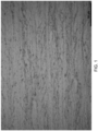
- FIG. 1 is an optical image of the alloy after processing. Typical grains and some indications of work are visible. Some Ni-Cr silicides are visible.
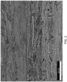
- FIG. 2 is a BSE SEM image.
- the dark spots are Cr-Ni-Mn-Si silicides. These silicides have particle sizes on the order of 100 nanometers to 200 nm. Their presence is unique, and their small size is unusual. It is noted that these silicides are not visible in FIG. 1 .
- a Cu-1.23Ni-0.38Si-0.23Cr-0.08Mn-0.02Zr alloy was cast, cold worked to a %CW of 85% to 95%, solution annealed at a temperature of 900° to 1000°C, and then aged twice.
- the first aging was performed for 24 hours at either 800°F, 815°F, or 825°F (427°C, 435°C, 441°C).
- the second aging was performed for six hours at 800°F (427°C).
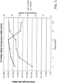
- the 0.2% offset yield strength (YS) and the electrical conductivity (%IACS) of the alloy were measured at various time points during the second aging, and are illustrated in three graphs.
- HV Hardness (HV) C18140M Annealed 51.9 88.5 C18140M Rolled/Aged 159.7 Cu-Ni-Si-Cr-Mn-Zr Annealed 57.4 100.0 Cu-Ni-Si-Cr-Mn-Zr Rolled/Aged 199.8 C18070 Annealed 52.3 89.8 C18070 Rolled/Aged 168.3 C18150 Annealed 58.3 92.7 C18150 Rolled/Aged 177.5
- HV Hardness (HV) Resistivity ( ⁇ -cm) Cu-Ni-Si-Cr-Mn-Zr 427 (800) 3 616 (89.4) 582 (84.5) 7.02 40.5 4.26 Cu-Ni-Si-Cr-Mn-Zr 427 (800) 3 626 (90.8) 587 (85.2) 7.77 39.7 187.1 4.34 Cu-Ni-Si-Cr-Mn-Zr 427 (800) 6 643 (93.3) 603 (87.5) 8.02 44.1 3.91 Cu-Ni-Si-Cr-Mn-Zr 427 (800) 6 639 (92.8) 601 (87.2) 7.63 44.5 198.9 3.88
- Strips comprising from 1.2 wt% to 1.4 wt% nickel; from 0.3 wt% to 4 wt% silicon; from 0.3 wt% to 0.4 wt% chromium; from 0.08 wt% to 0.12 wt% manganese; from 0.02 wt% to 0.06 wt% zirconium; and balance copper were made according to the present disclosure and tested.
- the alloys were cold worked and annealed.
- the samples were placed in a furnace at 441 °C (825°F) for six hours. Then, the furnace temperature was lowered to 427 °C (800°F), which took 30 minutes to 60 minutes. The samples were then heated for an additional six hours after the 441 °C (825°F) heating, totaling twelve hours time-in-furnace.
- UTS ultimate tensile strength
- YS 0.2% offset yield strength
- %TE total elongation to break
- EM elastic modulus
- electrical conductivity %lACS
Landscapes
- Chemical & Material Sciences (AREA)
- Engineering & Computer Science (AREA)
- Materials Engineering (AREA)
- Mechanical Engineering (AREA)
- Metallurgy (AREA)
- Organic Chemistry (AREA)
- Physics & Mathematics (AREA)
- Thermal Sciences (AREA)
- Crystallography & Structural Chemistry (AREA)
- Conductive Materials (AREA)
Claims (14)
- Kupferlegierung, umfassend:von 1,2 Gew.-% bis 1,4 Gew.-% Nickel,von 0,3 Gew.-% bis 0,4 Gew.-% Silicium,von 0,3 Gew.-% bis 0,4 Gew.-% Chrom,von 0,08 Gew.-% bis 0,12 Gew.-% Mangan,von 0,2 Gew.-% bis 0,06 Gew.-% Zirconium, undansonsten Kupfer und unvermeidliche Verunreinigungen,wobei die Legierung eine 0,2%-Dehngrenze von wenigstens 551 MPa und eine Leitfähigkeit von wenigstens 48% IACS aufweist.
- Kupferlegierung nach Anspruch 1, wobei die Legierung kein Beryllium, Titan, Eisen, Cobalt, Magnesium oder Bor enthält.
- Kupferlegierung nach Anspruch 1, wobei die Legierung eine Zugfestigkeit von wenigstens 606 MPa aufweist.
- Kupferlegierung nach Anspruch 1, wobei die Legierung ein Elastizitätsmodul von wenigstens 137,895 MPa aufweist.
- Kupferlegierung nach Anspruch 1, wobei die Legierung eine Bruchdehnung von wenigstens 8% aufweist.
- Kupferlegierung nach Anspruch 1, wobei die Legierung eine Duktilität von wenigstens 5% bis ungefähr 15% aufweist.
- Kupferlegierung nach Anspruch 1, wobei die Legierung ein Formbarkeitsverhältnis von 0,4/1 oder weniger aufweist.
- Kupferlegierung nach Anspruch 1, das Silicide aus Silicium, Chrom, Nickel und Mangan enthält.
- Kupferlegierung nach Anspruch 1, das eine 0,2%-Dehngrenze von wenigstens 551 MPa, eine Leitfähigkeit von wenigstens 48% IACS und eine Bruchdehnung von wenigstens 8% aufweist.
- Kupferlegierung nach Anspruch 1, das eine 0,2%-Dehngrenze von wenigstens 551 MPa, eine Leitfähigkeit von wenigstens 49% IACS und eine Zugfestigkeit von wenigstens 620 MPa aufweist.
- Verfahren zum Erhalten einer Kupferlegierung nach Anspruch 1, das kein Beryllium enthält, eine 0,2%-Dehngrenze von wenigstens 551 MPa und eine Leitfähigkeit von wenigstens 48% IACS aufweist, umfassend:Kaltumformen einer Kupfer-Nickel-Silicium-Chrom-Mangan-Zirconium-Legierung zu einem Prozentsatz einer Kaltumformung (% CW) von 80% bis 95%,Lösungsglühen der kaltumgeformten Kupfer-Nickel-Silicium-Chrom-Mangan-Zirconium-Legierung, undAushärten der lösungsgeglühten Kupfer-Nickel-Silicium-Chrom-Mangan-Zirconium-Legierung, um die Kupferlegierung mit einer 0,2%-Dehngrenze von wenigstens 551 MPa und einer Leitfähigkeit von wenigstens 48% IACS zu erhalten.
- Verfahren nach Anspruch 11, wobei das Lösungsglühen bei einer Temperatur von 900°C bis 1000°C für eine Zeitdauer von 5 Minuten bis 20 Minuten durchgeführt wird.
- Verfahren nach Anspruch 11, wobei das Aushärten bei einer Temperatur von 400°C bis 460°C für eine Zeitdauer von 6 Stunden bis 60 Stunden und vorzugsweise eine Zeitdauer von 6 Stunden bis 18 Stunden durchgeführt wird.
- Artikel, der aus der Kupferlegierung des Anspruchs 1 ausgebildet ist, wobei der Artikel eine Wärmesenke, ein elektrischer Steckverbinder, ein elektronischer Steckverbinder, ein Kabelbaumanschluss, ein Elektrofahrzeug-Ladekontakt, ein Hochspannung/-strom/-leistung-Anschlusskontakt, ein Stromsteckverbinderkontakt, ein Midplane-Steckverbinder, ein Backplane-Steckverbinder, ein Kartenkanten-Steckverbinder, ein Photovoltaiksystem-Steckverbinder, ein Geräte-Stromkontakt, ein Computer-Stromkontakt, ein Wärmespreizer, eine Buchsen- oder Lageroberfläche oder eine Komponente für ein elektronisches oder ein elektrisches Gerät ist.
Applications Claiming Priority (2)
| Application Number | Priority Date | Filing Date | Title |
|---|---|---|---|
| US201862696915P | 2018-07-12 | 2018-07-12 | |
| PCT/US2019/041556 WO2020014582A1 (en) | 2018-07-12 | 2019-07-12 | Copper-nickel-silicon alloys with high strength and high electrical conductivity |
Publications (2)
| Publication Number | Publication Date |
|---|---|
| EP3821046A1 EP3821046A1 (de) | 2021-05-19 |
| EP3821046B1 true EP3821046B1 (de) | 2025-04-09 |
Family
ID=67480358
Family Applications (1)
| Application Number | Title | Priority Date | Filing Date |
|---|---|---|---|
| EP19746289.8A Active EP3821046B1 (de) | 2018-07-12 | 2019-07-12 | Kupfer-nickel-silicium-legierungen mit hoher festigkeit und hoher elektrischer leitfähigkeit |
Country Status (7)
| Country | Link |
|---|---|
| US (2) | US20210130931A1 (de) |
| EP (1) | EP3821046B1 (de) |
| JP (1) | JP7574176B2 (de) |
| KR (1) | KR102786079B1 (de) |
| CN (1) | CN112823215A (de) |
| TW (1) | TWI878235B (de) |
| WO (1) | WO2020014582A1 (de) |
Families Citing this family (2)
| Publication number | Priority date | Publication date | Assignee | Title |
|---|---|---|---|---|
| CN115044801B (zh) * | 2022-08-16 | 2022-12-23 | 凯美龙精密铜板带(河南)有限公司 | 一种铜镍硅合金带材及其制备方法 |
| WO2025137269A1 (en) * | 2023-12-19 | 2025-06-26 | Materion Corporation | Method for strengthening a copper alloy |
Family Cites Families (14)
| Publication number | Priority date | Publication date | Assignee | Title |
|---|---|---|---|---|
| JPS57205007A (en) * | 1981-06-10 | 1982-12-16 | Hitachi Seiki Co Ltd | Automatic fixing and removing device of chuck click for machine tool |
| JPH06184680A (ja) * | 1992-12-21 | 1994-07-05 | Kobe Steel Ltd | 曲げ加工性が優れた銅合金 |
| JP2000080428A (ja) | 1998-08-31 | 2000-03-21 | Kobe Steel Ltd | 曲げ加工性が優れた銅合金板 |
| JP3800279B2 (ja) | 1998-08-31 | 2006-07-26 | 株式会社神戸製鋼所 | プレス打抜き性が優れた銅合金板 |
| JP2003257417A (ja) * | 2002-02-28 | 2003-09-12 | Nippon Mining & Metals Co Ltd | リチウムイオン2次電池用負極 |
| JP4566048B2 (ja) | 2005-03-31 | 2010-10-20 | 株式会社神戸製鋼所 | 曲げ加工性に優れた高強度銅合金板及びその製造方法 |
| JP2008223069A (ja) * | 2007-03-12 | 2008-09-25 | Miyoshi Gokin Kogyo Kk | 高強度高導電性銅合金及びその製造方法 |
| JP2008266787A (ja) | 2007-03-28 | 2008-11-06 | Furukawa Electric Co Ltd:The | 銅合金材およびその製造方法 |
| EP2221391B1 (de) * | 2007-11-05 | 2014-04-30 | The Furukawa Electric Co., Ltd. | Kupferlegierungsblech |
| JP2012229467A (ja) | 2011-04-26 | 2012-11-22 | Jx Nippon Mining & Metals Corp | 電子材料用Cu−Ni−Si系銅合金 |
| JP5688744B2 (ja) * | 2012-10-04 | 2015-03-25 | 株式会社日本製鋼所 | 高強度高靱性銅合金鍛造材 |
| JP6339361B2 (ja) | 2013-12-20 | 2018-06-06 | 古河電気工業株式会社 | 銅合金板材およびその製造方法 |
| CN106460099B (zh) * | 2014-05-30 | 2020-03-17 | 古河电气工业株式会社 | 铜合金板材、由铜合金板材构成的连接器和铜合金板材的制造方法 |
| JP6246174B2 (ja) | 2015-10-05 | 2017-12-13 | Jx金属株式会社 | 電子部品用Cu−Co−Ni−Si合金 |
-
2019
- 2019-07-12 JP JP2021500904A patent/JP7574176B2/ja active Active
- 2019-07-12 WO PCT/US2019/041556 patent/WO2020014582A1/en not_active Ceased
- 2019-07-12 CN CN201980059568.1A patent/CN112823215A/zh active Pending
- 2019-07-12 KR KR1020217004226A patent/KR102786079B1/ko active Active
- 2019-07-12 TW TW108124650A patent/TWI878235B/zh active
- 2019-07-12 US US17/259,710 patent/US20210130931A1/en not_active Abandoned
- 2019-07-12 EP EP19746289.8A patent/EP3821046B1/de active Active
-
2025
- 2025-03-05 US US19/071,327 patent/US20250197972A1/en active Pending
Also Published As
| Publication number | Publication date |
|---|---|
| TW202016324A (zh) | 2020-05-01 |
| TWI878235B (zh) | 2025-04-01 |
| JP7574176B2 (ja) | 2024-10-28 |
| CN112823215A (zh) | 2021-05-18 |
| EP3821046A1 (de) | 2021-05-19 |
| US20250197972A1 (en) | 2025-06-19 |
| KR102786079B1 (ko) | 2025-03-26 |
| US20210130931A1 (en) | 2021-05-06 |
| KR20210059699A (ko) | 2021-05-25 |
| WO2020014582A1 (en) | 2020-01-16 |
| JP2021531403A (ja) | 2021-11-18 |
Similar Documents
| Publication | Publication Date | Title |
|---|---|---|
| EP1520054B1 (de) | Cobalt, nickel und silicium enthaltende kupferlegierung | |
| JP4660735B2 (ja) | 銅基合金板材の製造方法 | |
| JP5466879B2 (ja) | 銅合金板材およびその製造方法 | |
| EP3438298B1 (de) | Kupferlegierung für elektronische/elektrische vorrichtungen, kupferlegierungsband für elektronische und elektrische vorrichtungen, komponente für elektronische und elektrische vorrichtung, endgerät, sammelschiene und bewegliches teil für relais | |
| EP2772560B1 (de) | Kupferlegierung für elektronische vorrichtungen, verfahren zur herstellung dieser legierung, aus dieser legierung gewalztes material, und aus dieser legierung gefertiges bauteil | |
| EP2508631A1 (de) | Folienmaterial aus kupferlegierung steckverbinder damit und verfahren zur herstellung eines folienmaterials aus kupferlegierung | |
| KR20140056003A (ko) | Cu-Ni-Co-Sⅰ계 구리 합금 판재 및 이의 제조법 | |
| JPH11335756A (ja) | 電子部品用銅合金板 | |
| US20250197972A1 (en) | Copper-nickel-silicon alloys with high strength and high electrical conductivity | |
| EP2940166B1 (de) | Kupferlegierung für elektrische und elektronische einrichtung, kupferlegierungsdünnschicht für elektrische und elektronische einrichtung sowie leitfähiges teil und endgerät für elektrische und elektronische einrichtung | |
| CN105154713A (zh) | 电子电气设备用铜合金、铜合金薄板、导电元件以及端子 | |
| JP5619389B2 (ja) | 銅合金材料 | |
| CN106460099A (zh) | 铜合金板材、由铜合金板材构成的连接器和铜合金板材的制造方法 | |
| JP7430502B2 (ja) | 銅合金線材及び電子機器部品 | |
| WO2009123159A1 (ja) | 電気電子機器用銅合金材料および電気電子部品 | |
| JP3717321B2 (ja) | 半導体リードフレーム用銅合金 | |
| CN104870672B (zh) | 电子电气设备用铜合金、电子电气设备用铜合金薄板、电子电气设备用导电元件及端子 | |
| EP2944703A1 (de) | Kupferlegierung für eine elektronische oder elektrische vorrichtung, kupferlegierungs-dünnschicht für eine elektronische oder elektrische vorrichtung, verfahren zur herstellung der kupferlegierung für eine elektronische oder elektrische vorrichtung, leitfähige komponente für die elektronische oder elektrische vorrichtung und endgerät | |
| CN107299248A (zh) | 电子电气设备用铜合金、铜合金薄板、导电元件及端子 | |
| JPH10195562A (ja) | 打抜加工性に優れた電気電子機器用銅合金およびその製造方法 | |
| EP3953495B1 (de) | Kupferlegierungen mit hoher festigkeit und hoher leitfähigkeit und verfahren zur herstellung solcher kupferlegierungen | |
| JP2016141878A (ja) | 銅合金条およびそれを備える大電流用電子部品及び放熱用電子部品 | |
| EP2940165A1 (de) | Kupferlegierung für elektrische und elektronische vorrichtungen, kupferlegierungsdünnschicht für elektrische und elektronische vorrichtungen sowie leitfähiges teil und endgerät für elektrische und elektronische vorrichtungen | |
| JP2013095977A (ja) | Cu−Ni−Si系合金及びその製造方法 | |
| JP4653239B2 (ja) | 電気電子機器用銅合金材料および電気電子部品 |
Legal Events
| Date | Code | Title | Description |
|---|---|---|---|
| STAA | Information on the status of an ep patent application or granted ep patent |
Free format text: STATUS: UNKNOWN |
|
| STAA | Information on the status of an ep patent application or granted ep patent |
Free format text: STATUS: THE INTERNATIONAL PUBLICATION HAS BEEN MADE |
|
| PUAI | Public reference made under article 153(3) epc to a published international application that has entered the european phase |
Free format text: ORIGINAL CODE: 0009012 |
|
| STAA | Information on the status of an ep patent application or granted ep patent |
Free format text: STATUS: REQUEST FOR EXAMINATION WAS MADE |
|
| 17P | Request for examination filed |
Effective date: 20210210 |
|
| AK | Designated contracting states |
Kind code of ref document: A1 Designated state(s): AL AT BE BG CH CY CZ DE DK EE ES FI FR GB GR HR HU IE IS IT LI LT LU LV MC MK MT NL NO PL PT RO RS SE SI SK SM TR |
|
| DAV | Request for validation of the european patent (deleted) | ||
| DAX | Request for extension of the european patent (deleted) | ||
| STAA | Information on the status of an ep patent application or granted ep patent |
Free format text: STATUS: EXAMINATION IS IN PROGRESS |
|
| 17Q | First examination report despatched |
Effective date: 20220420 |
|
| GRAP | Despatch of communication of intention to grant a patent |
Free format text: ORIGINAL CODE: EPIDOSNIGR1 |
|
| STAA | Information on the status of an ep patent application or granted ep patent |
Free format text: STATUS: GRANT OF PATENT IS INTENDED |
|
| RIC1 | Information provided on ipc code assigned before grant |
Ipc: H01B 1/02 20060101ALI20241008BHEP Ipc: C22F 1/00 20060101ALI20241008BHEP Ipc: C22F 1/08 20060101ALI20241008BHEP Ipc: C22C 9/06 20060101AFI20241008BHEP |
|
| INTG | Intention to grant announced |
Effective date: 20241031 |
|
| GRAS | Grant fee paid |
Free format text: ORIGINAL CODE: EPIDOSNIGR3 |
|
| GRAA | (expected) grant |
Free format text: ORIGINAL CODE: 0009210 |
|
| STAA | Information on the status of an ep patent application or granted ep patent |
Free format text: STATUS: THE PATENT HAS BEEN GRANTED |
|
| AK | Designated contracting states |
Kind code of ref document: B1 Designated state(s): AL AT BE BG CH CY CZ DE DK EE ES FI FR GB GR HR HU IE IS IT LI LT LU LV MC MK MT NL NO PL PT RO RS SE SI SK SM TR |
|
| REG | Reference to a national code |
Ref country code: GB Ref legal event code: FG4D |
|
| REG | Reference to a national code |
Ref country code: CH Ref legal event code: EP |
|
| REG | Reference to a national code |
Ref country code: DE Ref legal event code: R096 Ref document number: 602019068408 Country of ref document: DE |
|
| REG | Reference to a national code |
Ref country code: IE Ref legal event code: FG4D |
|
| REG | Reference to a national code |
Ref country code: NL Ref legal event code: MP Effective date: 20250409 |
|
| PG25 | Lapsed in a contracting state [announced via postgrant information from national office to epo] |
Ref country code: NL Free format text: LAPSE BECAUSE OF FAILURE TO SUBMIT A TRANSLATION OF THE DESCRIPTION OR TO PAY THE FEE WITHIN THE PRESCRIBED TIME-LIMIT Effective date: 20250409 |
|
| REG | Reference to a national code |
Ref country code: AT Ref legal event code: MK05 Ref document number: 1783581 Country of ref document: AT Kind code of ref document: T Effective date: 20250409 |
|
| PG25 | Lapsed in a contracting state [announced via postgrant information from national office to epo] |
Ref country code: ES Free format text: LAPSE BECAUSE OF FAILURE TO SUBMIT A TRANSLATION OF THE DESCRIPTION OR TO PAY THE FEE WITHIN THE PRESCRIBED TIME-LIMIT Effective date: 20250409 Ref country code: PT Free format text: LAPSE BECAUSE OF FAILURE TO SUBMIT A TRANSLATION OF THE DESCRIPTION OR TO PAY THE FEE WITHIN THE PRESCRIBED TIME-LIMIT Effective date: 20250811 Ref country code: FI Free format text: LAPSE BECAUSE OF FAILURE TO SUBMIT A TRANSLATION OF THE DESCRIPTION OR TO PAY THE FEE WITHIN THE PRESCRIBED TIME-LIMIT Effective date: 20250409 |
|
| PGFP | Annual fee paid to national office [announced via postgrant information from national office to epo] |
Ref country code: DE Payment date: 20250716 Year of fee payment: 7 |
|
| REG | Reference to a national code |
Ref country code: LT Ref legal event code: MG9D |
|
| PG25 | Lapsed in a contracting state [announced via postgrant information from national office to epo] |
Ref country code: GR Free format text: LAPSE BECAUSE OF FAILURE TO SUBMIT A TRANSLATION OF THE DESCRIPTION OR TO PAY THE FEE WITHIN THE PRESCRIBED TIME-LIMIT Effective date: 20250710 Ref country code: NO Free format text: LAPSE BECAUSE OF FAILURE TO SUBMIT A TRANSLATION OF THE DESCRIPTION OR TO PAY THE FEE WITHIN THE PRESCRIBED TIME-LIMIT Effective date: 20250709 |
|
| PG25 | Lapsed in a contracting state [announced via postgrant information from national office to epo] |
Ref country code: PL Free format text: LAPSE BECAUSE OF FAILURE TO SUBMIT A TRANSLATION OF THE DESCRIPTION OR TO PAY THE FEE WITHIN THE PRESCRIBED TIME-LIMIT Effective date: 20250409 |
|
| PG25 | Lapsed in a contracting state [announced via postgrant information from national office to epo] |
Ref country code: BG Free format text: LAPSE BECAUSE OF FAILURE TO SUBMIT A TRANSLATION OF THE DESCRIPTION OR TO PAY THE FEE WITHIN THE PRESCRIBED TIME-LIMIT Effective date: 20250409 |
|
| PG25 | Lapsed in a contracting state [announced via postgrant information from national office to epo] |
Ref country code: HR Free format text: LAPSE BECAUSE OF FAILURE TO SUBMIT A TRANSLATION OF THE DESCRIPTION OR TO PAY THE FEE WITHIN THE PRESCRIBED TIME-LIMIT Effective date: 20250409 |
|
| PG25 | Lapsed in a contracting state [announced via postgrant information from national office to epo] |
Ref country code: AT Free format text: LAPSE BECAUSE OF FAILURE TO SUBMIT A TRANSLATION OF THE DESCRIPTION OR TO PAY THE FEE WITHIN THE PRESCRIBED TIME-LIMIT Effective date: 20250409 |
|
| PG25 | Lapsed in a contracting state [announced via postgrant information from national office to epo] |
Ref country code: RS Free format text: LAPSE BECAUSE OF FAILURE TO SUBMIT A TRANSLATION OF THE DESCRIPTION OR TO PAY THE FEE WITHIN THE PRESCRIBED TIME-LIMIT Effective date: 20250709 |
|
| PG25 | Lapsed in a contracting state [announced via postgrant information from national office to epo] |
Ref country code: IS Free format text: LAPSE BECAUSE OF FAILURE TO SUBMIT A TRANSLATION OF THE DESCRIPTION OR TO PAY THE FEE WITHIN THE PRESCRIBED TIME-LIMIT Effective date: 20250809 |
|
| PG25 | Lapsed in a contracting state [announced via postgrant information from national office to epo] |
Ref country code: LV Free format text: LAPSE BECAUSE OF FAILURE TO SUBMIT A TRANSLATION OF THE DESCRIPTION OR TO PAY THE FEE WITHIN THE PRESCRIBED TIME-LIMIT Effective date: 20250409 |
|
| REG | Reference to a national code |
Ref country code: DE Ref legal event code: R097 Ref document number: 602019068408 Country of ref document: DE |
|
| PG25 | Lapsed in a contracting state [announced via postgrant information from national office to epo] |
Ref country code: SM Free format text: LAPSE BECAUSE OF FAILURE TO SUBMIT A TRANSLATION OF THE DESCRIPTION OR TO PAY THE FEE WITHIN THE PRESCRIBED TIME-LIMIT Effective date: 20250409 Ref country code: DK Free format text: LAPSE BECAUSE OF FAILURE TO SUBMIT A TRANSLATION OF THE DESCRIPTION OR TO PAY THE FEE WITHIN THE PRESCRIBED TIME-LIMIT Effective date: 20250409 |
|
| PG25 | Lapsed in a contracting state [announced via postgrant information from national office to epo] |
Ref country code: CZ Free format text: LAPSE BECAUSE OF FAILURE TO SUBMIT A TRANSLATION OF THE DESCRIPTION OR TO PAY THE FEE WITHIN THE PRESCRIBED TIME-LIMIT Effective date: 20250409 |
|
| PG25 | Lapsed in a contracting state [announced via postgrant information from national office to epo] |
Ref country code: EE Free format text: LAPSE BECAUSE OF FAILURE TO SUBMIT A TRANSLATION OF THE DESCRIPTION OR TO PAY THE FEE WITHIN THE PRESCRIBED TIME-LIMIT Effective date: 20250409 |
|
| PG25 | Lapsed in a contracting state [announced via postgrant information from national office to epo] |
Ref country code: RO Free format text: LAPSE BECAUSE OF FAILURE TO SUBMIT A TRANSLATION OF THE DESCRIPTION OR TO PAY THE FEE WITHIN THE PRESCRIBED TIME-LIMIT Effective date: 20250409 Ref country code: SK Free format text: LAPSE BECAUSE OF FAILURE TO SUBMIT A TRANSLATION OF THE DESCRIPTION OR TO PAY THE FEE WITHIN THE PRESCRIBED TIME-LIMIT Effective date: 20250409 |
|
| PG25 | Lapsed in a contracting state [announced via postgrant information from national office to epo] |
Ref country code: IT Free format text: LAPSE BECAUSE OF FAILURE TO SUBMIT A TRANSLATION OF THE DESCRIPTION OR TO PAY THE FEE WITHIN THE PRESCRIBED TIME-LIMIT Effective date: 20250409 |
|
| PLBE | No opposition filed within time limit |
Free format text: ORIGINAL CODE: 0009261 |
|
| STAA | Information on the status of an ep patent application or granted ep patent |
Free format text: STATUS: NO OPPOSITION FILED WITHIN TIME LIMIT |
|
| REG | Reference to a national code |
Ref country code: CH Ref legal event code: L10 Free format text: ST27 STATUS EVENT CODE: U-0-0-L10-L00 (AS PROVIDED BY THE NATIONAL OFFICE) Effective date: 20260218 |
|
| REG | Reference to a national code |
Ref country code: CH Ref legal event code: H13 Free format text: ST27 STATUS EVENT CODE: U-0-0-H10-H13 (AS PROVIDED BY THE NATIONAL OFFICE) Effective date: 20260224 |
|
| PG25 | Lapsed in a contracting state [announced via postgrant information from national office to epo] |
Ref country code: LU Free format text: LAPSE BECAUSE OF NON-PAYMENT OF DUE FEES Effective date: 20250712 |
|
| 26N | No opposition filed |
Effective date: 20260112 |
|
| GBPC | Gb: european patent ceased through non-payment of renewal fee |
Effective date: 20250712 |
|
| REG | Reference to a national code |
Ref country code: BE Ref legal event code: MM Effective date: 20250731 |
|
| PG25 | Lapsed in a contracting state [announced via postgrant information from national office to epo] |
Ref country code: GB Free format text: LAPSE BECAUSE OF NON-PAYMENT OF DUE FEES Effective date: 20250712 |
|
| PG25 | Lapsed in a contracting state [announced via postgrant information from national office to epo] |
Ref country code: BE Free format text: LAPSE BECAUSE OF NON-PAYMENT OF DUE FEES Effective date: 20250731 |
|
| PG25 | Lapsed in a contracting state [announced via postgrant information from national office to epo] |
Ref country code: FR Free format text: LAPSE BECAUSE OF NON-PAYMENT OF DUE FEES Effective date: 20250731 |
|
| PG25 | Lapsed in a contracting state [announced via postgrant information from national office to epo] |
Ref country code: CH Free format text: LAPSE BECAUSE OF NON-PAYMENT OF DUE FEES Effective date: 20250731 |
|
| PG25 | Lapsed in a contracting state [announced via postgrant information from national office to epo] |
Ref country code: LT Free format text: LAPSE BECAUSE OF FAILURE TO SUBMIT A TRANSLATION OF THE DESCRIPTION OR TO PAY THE FEE WITHIN THE PRESCRIBED TIME-LIMIT Effective date: 20250409 |
|
| PG25 | Lapsed in a contracting state [announced via postgrant information from national office to epo] |
Ref country code: IE Free format text: LAPSE BECAUSE OF NON-PAYMENT OF DUE FEES Effective date: 20250712 |
|
| PG25 | Lapsed in a contracting state [announced via postgrant information from national office to epo] |
Ref country code: MC Free format text: LAPSE BECAUSE OF FAILURE TO SUBMIT A TRANSLATION OF THE DESCRIPTION OR TO PAY THE FEE WITHIN THE PRESCRIBED TIME-LIMIT Effective date: 20250409 |
|
| PG25 | Lapsed in a contracting state [announced via postgrant information from national office to epo] |
Ref country code: CY Free format text: LAPSE BECAUSE OF FAILURE TO SUBMIT A TRANSLATION OF THE DESCRIPTION OR TO PAY THE FEE WITHIN THE PRESCRIBED TIME-LIMIT Effective date: 20250409 Ref country code: SE Free format text: LAPSE BECAUSE OF FAILURE TO SUBMIT A TRANSLATION OF THE DESCRIPTION OR TO PAY THE FEE WITHIN THE PRESCRIBED TIME-LIMIT Effective date: 20250409 |