EP3772088A2 - Verfahren zur verbindung von chips mittels planarisierter chipverbindungsvorformen - Google Patents
Verfahren zur verbindung von chips mittels planarisierter chipverbindungsvorformen Download PDFInfo
- Publication number
- EP3772088A2 EP3772088A2 EP20189191.8A EP20189191A EP3772088A2 EP 3772088 A2 EP3772088 A2 EP 3772088A2 EP 20189191 A EP20189191 A EP 20189191A EP 3772088 A2 EP3772088 A2 EP 3772088A2
- Authority
- EP
- European Patent Office
- Prior art keywords
- die
- attach
- semiconductor die
- preforms
- graphite pad
- Prior art date
- Legal status (The legal status is an assumption and is not a legal conclusion. Google has not performed a legal analysis and makes no representation as to the accuracy of the status listed.)
- Pending
Links
Images


Classifications
-
- H10P72/78—
-
- H10W72/0113—
-
- H10W72/01212—
-
- H10W72/01261—
-
- H10W72/01304—
-
- H10W72/01336—
-
- H10W72/01351—
-
- H10W72/07141—
-
- H10W72/07178—
-
- H10W72/07183—
-
- H10W72/072—
-
- H10W72/073—
-
- H10W72/07331—
-
- H10W72/07332—
-
- H10W72/252—
-
- H10W72/325—
-
- H10W72/352—
-
- H10W90/734—
-
- H10W90/736—
Definitions
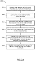
- the die-attach film may be bonded to the semiconductor die using heat and pressure.
- the semiconductor die is then removed from the film, the portion of the film disposed beneath the semiconductor die may adhere to the bottom surface of the semiconductor die.
- the semiconductor die including the layer of die-attach material may be coupled to a product substrate (e.g., printed circuit board (PCB), ceramic substrate, integrated circuit device, multi-chip module, and the like) by sintering the die-attach material layer.
- PCB printed circuit board
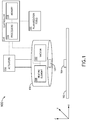
- suction forces may be used to temporarily couple a semiconductor die 120 to the handling tool 106.
- the suction forces may be used in addition to, or in lieu of, the graphite pad 126 to enable efficient and reliable handling.
- the suction forces may be applied through both the vacuum port 128 and the graphite pad 126.
- a graphite pad 126 may be formed on the surface 124 of the handling tool 106 such that the graphite pad 126 completely or partially covers the one or more vacuum ports 128.
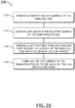
- a second surface of the semiconductor die 120 is bonded to at least one die-attach preform 104 (e.g., sintered silver preform 104).
- the controller 114 may generate one or more control signals configured to cause the actuators 112 to actuate the handling tool 106 in order to bring the lower surface of the semiconductor die 120 into contact with an upper surface of a sintered silver preform 104.
- the handling tool 106 may apply a first pressure between the graphite pad 126 and the upper surface of the semiconductor die 120, and a second pressure between the lower surface of the semiconductor die 120 and the upper surface of a sintered silver preform 104.
- the controller 114 may generate one or more control signals configured to cause the one or more heating elements 108 to generate heat such that heat may be applied through the surface 124 of the handling tool 106 and through the graphite pad 126/semiconductor die 120 to the joint surface between the semiconductor die 120 and sintered silver preform 104.
- the temperature required for bonding the lower surface of the semiconductor die 120 and the upper surface of the die-attach preform 104 may depend on the material of the die-attach preform 104.
- the semiconductor die 120 may be coupled to a product substrate.
- a product substrate may include any product substrate configured to receive a semiconductor die 120 including, but not limited to, a ceramic substrate, a printed circuit board (PCB), an integrated circuit, a package body (e.g., quad flat no-lead (QFN) package), and the like.
- the controller 114 may generate one or more control signals configured to cause the actuators 112 to actuate the handling tool 106 in order to bring a lower surface of the die-attach preform 104 coupled to the semiconductor die 120 into contact with an upper surface of a product substrate.
- the controller 114 may then generate one or more control signals configured to cause the one or more heating elements 108 to generate heat such that heat may be applied through the surface 124 of the handling tool 106, graphite pad 126, semiconductor die 120, and die-attach preform 104 to the joint surface between the die-attach preform 104 and a surface of the product substrate.
- the heating elements 108 may be used to sinter the die-attach preform 104 coupled to a semiconductor die 120 in order to couple the semiconductor die 120 to the product substrate.
- the use of the handling tool 106 for handling the various components of the present disclosure may provide for improved precision tooling, flexible size options, and fabrication of high-density product substrates.
- the use of a handling tool 106 actuatable via a controller 114 may enable die-attach preforms 104 and semiconductor die 120 to be fabricated and/or disposed adjacent to one another, thereby enabling further miniaturization of product substrates.
- Embodiments of the present disclosure are directed to a novel die-attach material, process, and tooling approach for optimal thermal and RF performance of semiconductor die 120. As compared to conventional approaches, it is contemplated herein that the system 100 and method 200 of the present disclosure may enable significant improvements in automation speed and throughput, as well as improvements in performance, yield, component miniaturization, and overall cost.
- the one or more components of system 100 may be communicatively coupled to the various other components of system 100 in any manner known in the art.
- the one or more processors 116 may be communicatively coupled to each other and other components via a wireline (e.g., copper wire, fiber optic cable, and the like) or wireless connection (e.g., RF coupling, IR coupling, data network communication (e.g., WiFi, WiMax, Bluetooth, 3G, 4G, 4G LTE, 5G and the like).
- the memory 118 may include any storage medium known in the art suitable for storing program instructions executable by the associated one or more processors 116.
- the memory 118 may include a non-transitory memory medium.
- the memory 118 may include, but is not limited to, a read-only memory (ROM), a random-access memory (RAM), a magnetic or optical memory device (e.g., disk), a magnetic tape, a solid-state drive and the like.
- ROM read-only memory
- RAM random-access memory
- magnetic or optical memory device e.g., disk
- magnetic tape e.g., magnetic tape
- solid-state drive e.g., solid-state drive and the like.
- memory 118 may be housed in a common controller housing with the one or more processors 116.
- the memory 118 may be located remotely with respect to the physical location of the processors 116, controller 114, and the like.
- the memory 118 maintains program instructions for causing the one or more processors 116 to carry out
Landscapes
- Engineering & Computer Science (AREA)
- Computer Hardware Design (AREA)
- Microelectronics & Electronic Packaging (AREA)
- Power Engineering (AREA)
- Manufacturing & Machinery (AREA)
- Die Bonding (AREA)
- Physics & Mathematics (AREA)
- Condensed Matter Physics & Semiconductors (AREA)
- General Physics & Mathematics (AREA)
- Wire Bonding (AREA)
Applications Claiming Priority (1)
| Application Number | Priority Date | Filing Date | Title |
|---|---|---|---|
| US16/530,016 US11373976B2 (en) | 2019-08-02 | 2019-08-02 | System and method for extreme performance die attach |
Publications (2)
| Publication Number | Publication Date |
|---|---|
| EP3772088A2 true EP3772088A2 (de) | 2021-02-03 |
| EP3772088A3 EP3772088A3 (de) | 2021-05-12 |
Family
ID=71948424
Family Applications (1)
| Application Number | Title | Priority Date | Filing Date |
|---|---|---|---|
| EP20189191.8A Pending EP3772088A3 (de) | 2019-08-02 | 2020-08-03 | Verfahren zur verbindung von chips mittels planarisierter chipverbindungsvorformen |
Country Status (2)
| Country | Link |
|---|---|
| US (1) | US11373976B2 (de) |
| EP (1) | EP3772088A3 (de) |
Cited By (1)
| Publication number | Priority date | Publication date | Assignee | Title |
|---|---|---|---|---|
| US11764185B2 (en) | 2021-08-31 | 2023-09-19 | Infineon Technologies Austria Ag | Diffusion soldering preform with varying surface profile |
Citations (1)
| Publication number | Priority date | Publication date | Assignee | Title |
|---|---|---|---|---|
| US7830021B1 (en) | 2005-09-06 | 2010-11-09 | Rockwell Collins, Inc. | Tamper resistant packaging with transient liquid phase bonding |
Family Cites Families (12)
| Publication number | Priority date | Publication date | Assignee | Title |
|---|---|---|---|---|
| DE3777995D1 (de) * | 1986-12-22 | 1992-05-07 | Siemens Ag | Verfahren zur befestigung von elektronischen bauelementen auf einem substrat, folie zur durchfuehrung des verfahrens und verfahren zur herstellung der folie. |
| US6875636B2 (en) * | 2003-07-14 | 2005-04-05 | Delphi Technologies, Inc. | Wafer applied thermally conductive interposer |
| WO2008096648A1 (ja) * | 2007-02-09 | 2008-08-14 | Nippon Mining & Metals Co., Ltd. | 高融点金属合金、高融点金属珪化物、高融点金属炭化物、高融点金属窒化物あるいは高融点金属ホウ化物の難焼結体からなるターゲット及びその製造方法並びに同スパッタリングターゲット-バッキングプレート組立体及びその製造方法 |
| DE102009018541A1 (de) * | 2009-04-24 | 2010-10-28 | W.C. Heraeus Gmbh | Kontaktierungsmittel und Verfahren zur Kontaktierung elektrischer Bauteile |
| US8716864B2 (en) * | 2012-06-07 | 2014-05-06 | Ixys Corporation | Solderless die attach to a direct bonded aluminum substrate |
| US9099567B2 (en) * | 2013-11-25 | 2015-08-04 | Freescale Semiconductor, Inc. | Packaged semiconductor devices and methods of their fabrication |
| MX2016012036A (es) * | 2014-05-05 | 2017-01-19 | Heraeus Deutschland Gmbh & Co Kg | Metodo para aplicar una preparacion de sinterizacion de metal seca mediante un sustrato de transferencia sobre un sustrato para componentes electronicos, sustrato correspondiente y su uso para la conexion sinterizada a los componentes electronicos. |
| EP3154729A4 (de) * | 2014-06-12 | 2018-02-28 | Alpha Metals, Inc. | Sintermaterialien und befestigungsverfahren damit |
| DE102014111744B4 (de) * | 2014-08-18 | 2022-01-05 | Infineon Technologies Ag | Baugruppe zum handhaben eines halbleiterchips und verfahren zum handhaben eines halbleiterchips |
| DE102014117020A1 (de) * | 2014-11-20 | 2016-05-25 | Infineon Technologies Ag | Verfahren zum herstellen einer stoffschlüssigen verbindung zwischen einem halbleiterchip und einer metallschicht |
| EP3587020A4 (de) * | 2017-02-23 | 2020-01-01 | Osaka University | Verbindungselement, verfahren zur herstellung des verbindungselements und verfahren zur herstellung der verbindungsstruktur |
| JP7252798B2 (ja) * | 2019-03-15 | 2023-04-05 | 日東電工株式会社 | 焼結接合用シートおよび基材付き焼結接合用シート |
-
2019
- 2019-08-02 US US16/530,016 patent/US11373976B2/en active Active
-
2020
- 2020-08-03 EP EP20189191.8A patent/EP3772088A3/de active Pending
Patent Citations (1)
| Publication number | Priority date | Publication date | Assignee | Title |
|---|---|---|---|---|
| US7830021B1 (en) | 2005-09-06 | 2010-11-09 | Rockwell Collins, Inc. | Tamper resistant packaging with transient liquid phase bonding |
Cited By (1)
| Publication number | Priority date | Publication date | Assignee | Title |
|---|---|---|---|---|
| US11764185B2 (en) | 2021-08-31 | 2023-09-19 | Infineon Technologies Austria Ag | Diffusion soldering preform with varying surface profile |
Also Published As
| Publication number | Publication date |
|---|---|
| US20210202433A1 (en) | 2021-07-01 |
| EP3772088A3 (de) | 2021-05-12 |
| US11373976B2 (en) | 2022-06-28 |
Similar Documents
| Publication | Publication Date | Title |
|---|---|---|
| JP7489956B2 (ja) | 焼結材料、及びそれを用いる接着方法 | |
| KR102305501B1 (ko) | 소결 재료 및 이를 이용한 부착 방법 | |
| JP5955392B2 (ja) | 金属成形体とパワー半導体の間に、太径ワイヤ又はストリップとのボンディングに使用する接続部を形成する方法 | |
| EP3772088A2 (de) | Verfahren zur verbindung von chips mittels planarisierter chipverbindungsvorformen | |
| KR20170030542A (ko) | 기판 어댑터를 제조하기 위한 방법, 기판 어댑터 및 반도체 소자와 접촉시키기 위한 방법 | |
| CN107851632B (zh) | 用于制造半导体器件的方法及相应的器件 | |
| KR20030094026A (ko) | 본딩 스테이지 | |
| WO2021157470A1 (ja) | 裁断装置、接合材転写装置および実装装置 | |
| KR102434064B1 (ko) | 세라믹 기판 제조 방법 | |
| US11440310B2 (en) | Method for producing a substrate adapter and substrate adapter for connecting to an electronic component | |
| JP2002280705A (ja) | 複合基板の回路形成方法及び複合基板 | |
| JP2005166936A (ja) | ダイ成形方法 | |
| KR20240139062A (ko) | 라미네이팅된 모듈식 프리폼을 사용하여 전기 및 기계 컴포넌트를 접합하는 방법 | |
| CN113140465A (zh) | 使用银烧结制造的直接接合铜衬底 | |
| JP7814521B2 (ja) | 積層モジュールプリフォームを使用して電気部品及び機械部品を接合する方法 | |
| JP2005236112A (ja) | 半導体装置の製造方法 | |
| CN217239420U (zh) | 芯片搬运装置及系统 | |
| JP2021086911A (ja) | デバイスの製造方法および接合装置、半導体デバイス | |
| KR20210007253A (ko) | 방열 기판 및 그 제조 방법 | |
| JP2007005366A (ja) | 半導体装置の製造方法 | |
| JPH0424188B2 (de) | ||
| JP2003048209A (ja) | セラミックチップの製造方法 |
Legal Events
| Date | Code | Title | Description |
|---|---|---|---|
| PUAI | Public reference made under article 153(3) epc to a published international application that has entered the european phase |
Free format text: ORIGINAL CODE: 0009012 |
|
| STAA | Information on the status of an ep patent application or granted ep patent |
Free format text: STATUS: THE APPLICATION HAS BEEN PUBLISHED |
|
| AK | Designated contracting states |
Kind code of ref document: A2 Designated state(s): AL AT BE BG CH CY CZ DE DK EE ES FI FR GB GR HR HU IE IS IT LI LT LU LV MC MK MT NL NO PL PT RO RS SE SI SK SM TR |
|
| AX | Request for extension of the european patent |
Extension state: BA ME |
|
| PUAL | Search report despatched |
Free format text: ORIGINAL CODE: 0009013 |
|
| AK | Designated contracting states |
Kind code of ref document: A3 Designated state(s): AL AT BE BG CH CY CZ DE DK EE ES FI FR GB GR HR HU IE IS IT LI LT LU LV MC MK MT NL NO PL PT RO RS SE SI SK SM TR |
|
| RIC1 | Information provided on ipc code assigned before grant |
Ipc: H01L 21/60 20060101AFI20210407BHEP Ipc: H01L 21/67 20060101ALI20210407BHEP |
|
| STAA | Information on the status of an ep patent application or granted ep patent |
Free format text: STATUS: REQUEST FOR EXAMINATION WAS MADE |
|
| 17P | Request for examination filed |
Effective date: 20211108 |
|
| RBV | Designated contracting states (corrected) |
Designated state(s): AL AT BE BG CH CY CZ DE DK EE ES FI FR GB GR HR HU IE IS IT LI LT LU LV MC MK MT NL NO PL PT RO RS SE SI SK SM TR |
|
| STAA | Information on the status of an ep patent application or granted ep patent |
Free format text: STATUS: EXAMINATION IS IN PROGRESS |
|
| 17Q | First examination report despatched |
Effective date: 20250211 |