EP3772088A2 - Method for die attach using planarized die-attach preforms - Google Patents
Method for die attach using planarized die-attach preforms Download PDFInfo
- Publication number
- EP3772088A2 EP3772088A2 EP20189191.8A EP20189191A EP3772088A2 EP 3772088 A2 EP3772088 A2 EP 3772088A2 EP 20189191 A EP20189191 A EP 20189191A EP 3772088 A2 EP3772088 A2 EP 3772088A2
- Authority
- EP
- European Patent Office
- Prior art keywords
- die
- attach
- semiconductor die
- preforms
- graphite pad
- Prior art date
- Legal status (The legal status is an assumption and is not a legal conclusion. Google has not performed a legal analysis and makes no representation as to the accuracy of the status listed.)
- Pending
Links
Images


Classifications
-
- H10P72/78—
-
- H10W72/0113—
-
- H10W72/01212—
-
- H10W72/01261—
-
- H10W72/01304—
-
- H10W72/01336—
-
- H10W72/01351—
-
- H10W72/07141—
-
- H10W72/07178—
-
- H10W72/07183—
-
- H10W72/072—
-
- H10W72/073—
-
- H10W72/07331—
-
- H10W72/07332—
-
- H10W72/252—
-
- H10W72/325—
-
- H10W72/352—
-
- H10W90/734—
-
- H10W90/736—
Definitions
- the die-attach film may be bonded to the semiconductor die using heat and pressure.
- the semiconductor die is then removed from the film, the portion of the film disposed beneath the semiconductor die may adhere to the bottom surface of the semiconductor die.
- the semiconductor die including the layer of die-attach material may be coupled to a product substrate (e.g., printed circuit board (PCB), ceramic substrate, integrated circuit device, multi-chip module, and the like) by sintering the die-attach material layer.
- PCB printed circuit board
- suction forces may be used to temporarily couple a semiconductor die 120 to the handling tool 106.
- the suction forces may be used in addition to, or in lieu of, the graphite pad 126 to enable efficient and reliable handling.
- the suction forces may be applied through both the vacuum port 128 and the graphite pad 126.
- a graphite pad 126 may be formed on the surface 124 of the handling tool 106 such that the graphite pad 126 completely or partially covers the one or more vacuum ports 128.
- a second surface of the semiconductor die 120 is bonded to at least one die-attach preform 104 (e.g., sintered silver preform 104).
- the controller 114 may generate one or more control signals configured to cause the actuators 112 to actuate the handling tool 106 in order to bring the lower surface of the semiconductor die 120 into contact with an upper surface of a sintered silver preform 104.
- the handling tool 106 may apply a first pressure between the graphite pad 126 and the upper surface of the semiconductor die 120, and a second pressure between the lower surface of the semiconductor die 120 and the upper surface of a sintered silver preform 104.
- the controller 114 may generate one or more control signals configured to cause the one or more heating elements 108 to generate heat such that heat may be applied through the surface 124 of the handling tool 106 and through the graphite pad 126/semiconductor die 120 to the joint surface between the semiconductor die 120 and sintered silver preform 104.
- the temperature required for bonding the lower surface of the semiconductor die 120 and the upper surface of the die-attach preform 104 may depend on the material of the die-attach preform 104.
- the semiconductor die 120 may be coupled to a product substrate.
- a product substrate may include any product substrate configured to receive a semiconductor die 120 including, but not limited to, a ceramic substrate, a printed circuit board (PCB), an integrated circuit, a package body (e.g., quad flat no-lead (QFN) package), and the like.
- the controller 114 may generate one or more control signals configured to cause the actuators 112 to actuate the handling tool 106 in order to bring a lower surface of the die-attach preform 104 coupled to the semiconductor die 120 into contact with an upper surface of a product substrate.
- the controller 114 may then generate one or more control signals configured to cause the one or more heating elements 108 to generate heat such that heat may be applied through the surface 124 of the handling tool 106, graphite pad 126, semiconductor die 120, and die-attach preform 104 to the joint surface between the die-attach preform 104 and a surface of the product substrate.
- the heating elements 108 may be used to sinter the die-attach preform 104 coupled to a semiconductor die 120 in order to couple the semiconductor die 120 to the product substrate.
- the use of the handling tool 106 for handling the various components of the present disclosure may provide for improved precision tooling, flexible size options, and fabrication of high-density product substrates.
- the use of a handling tool 106 actuatable via a controller 114 may enable die-attach preforms 104 and semiconductor die 120 to be fabricated and/or disposed adjacent to one another, thereby enabling further miniaturization of product substrates.
- Embodiments of the present disclosure are directed to a novel die-attach material, process, and tooling approach for optimal thermal and RF performance of semiconductor die 120. As compared to conventional approaches, it is contemplated herein that the system 100 and method 200 of the present disclosure may enable significant improvements in automation speed and throughput, as well as improvements in performance, yield, component miniaturization, and overall cost.
- the one or more components of system 100 may be communicatively coupled to the various other components of system 100 in any manner known in the art.
- the one or more processors 116 may be communicatively coupled to each other and other components via a wireline (e.g., copper wire, fiber optic cable, and the like) or wireless connection (e.g., RF coupling, IR coupling, data network communication (e.g., WiFi, WiMax, Bluetooth, 3G, 4G, 4G LTE, 5G and the like).
- the memory 118 may include any storage medium known in the art suitable for storing program instructions executable by the associated one or more processors 116.
- the memory 118 may include a non-transitory memory medium.
- the memory 118 may include, but is not limited to, a read-only memory (ROM), a random-access memory (RAM), a magnetic or optical memory device (e.g., disk), a magnetic tape, a solid-state drive and the like.
- ROM read-only memory
- RAM random-access memory
- magnetic or optical memory device e.g., disk
- magnetic tape e.g., magnetic tape
- solid-state drive e.g., solid-state drive and the like.
- memory 118 may be housed in a common controller housing with the one or more processors 116.
- the memory 118 may be located remotely with respect to the physical location of the processors 116, controller 114, and the like.
- the memory 118 maintains program instructions for causing the one or more processors 116 to carry out
Landscapes
- Engineering & Computer Science (AREA)
- Computer Hardware Design (AREA)
- Microelectronics & Electronic Packaging (AREA)
- Power Engineering (AREA)
- Manufacturing & Machinery (AREA)
- Die Bonding (AREA)
- Physics & Mathematics (AREA)
- Condensed Matter Physics & Semiconductors (AREA)
- General Physics & Mathematics (AREA)
- Wire Bonding (AREA)
Abstract
Description
- Semiconductor die-attach materials play a significant role in the reliability and thermal resistance of bonded semiconductor die used in chips and integrated circuits. Sintered silver materials have become increasingly popular die-attach materials for high-power device applications, as well as in contexts which require extremely low thermal resistance interfaces between the semiconductor die and the associated substrate. For example, sintered nano-silver films have been found to exhibit low thermal resistance and excellent adhesion.
- In order to bond semiconductor die to the die-attach materials, die-attach materials are typically formed into large die-attach films. The die-attach films may be formed on top of a polymer release film, which may then be deposed on a compliant material (e.g., rubber sheet). Subsequently, the semiconductor die are pressed against the film such that the die-attach film is lightly bonded, or "tacked," to the bottom surface of the semiconductor die. The rubber sheet may then cause the die-attach film to deform around the edges of the semiconductor die such that the edges of the semiconductor die cut the film into the shape of the semiconductor die, and the portion of the die-attach film tacked to the bottom surface of the semiconductor die is separated from the larger die-attach film. The die-attach film may be bonded to the semiconductor die using heat and pressure. When the semiconductor die is then removed from the film, the portion of the film disposed beneath the semiconductor die may adhere to the bottom surface of the semiconductor die. Subsequently, the semiconductor die including the layer of die-attach material may be coupled to a product substrate (e.g., printed circuit board (PCB), ceramic substrate, integrated circuit device, multi-chip module, and the like) by sintering the die-attach material layer.
- This traditional method of coupling die-attach materials to semiconductor die suffers from multiple drawbacks. First, this traditional approach is typically only feasible with larger semiconductor die (e.g., die larger than 0.05" x 0.05"). With smaller die, the force required to locally cut the film such that the film may adhere to the die and separate from the film sheet is large enough to damage the small die. Secondly, using the die edges to cut the die-attach often is not an efficient and/or reliable process. With die of all sizes, the edges of the die may not cut the die-attach film cleanly during transfer. Furthermore, many semiconductor die include non-planar circuitry and other structures on a surface of the die which may be damaged when force is applied to the top surface of the die during the die-attach transfer processes.
- Therefore, there exists a need in the art for a system and method which address one or more of the shortfalls of previous approaches identified above.
- A method for fabricating semiconductor die with die-attach preforms is disclosed. In embodiments, the method includes: applying an uncured die-attach paste material to a surface of a forming substrate to form one or more die-attach preforms, the surface of the forming substrate formed from a hydrophobic material; curing the one or more die-attach preforms; performing one or more planarization processes on the one or more die-attach preforms; coupling a first surface of a semiconductor die to a handling tool; and bonding a second surface of the semiconductor die to at least one die-attach preform of the one or more die-attach preforms.
- A method for fabricating semiconductor die with die-attach preforms is disclosed. In embodiments, the method includes: forming one or more die-attach preforms on a forming substrate; performing one or more planarization processes on the one or more die-attach preforms; forming a graphite pad on a surface of a handling tool; coupling the graphite pad to a first surface of a semiconductor die; and bonding a second surface of the semiconductor die to at least one die-attach preform of the one or more die-attach preforms, wherein the at least one die-attach preform substantially conforms to a shape and size of the second surface of the semiconductor die.
- This Summary is provided solely as an introduction to subject matter that is fully described in the Detailed Description and Drawings. The Summary should not be considered to describe essential features nor be used to determine the scope of the Claims. Moreover, it is to be understood that both the foregoing Summary and the following Detailed Description are provided for example only and are not necessarily restrictive of the subject matter claimed.
- The detailed description is described with reference to the accompanying figures. The use of the same reference numbers in different instances in the description and the figures may indicate similar or identical items. Various embodiments or examples ("examples") of the present disclosure are disclosed in the following detailed description and the accompanying drawings. The drawings are not necessarily to scale. In general, operations of disclosed processes may be performed in an arbitrary order, unless otherwise provided in the claims. In the drawings:
-
FIG. 1 illustrates a simplified block diagram view of a system for attaching semiconductor die to a die-attach preform, in accordance with one or more embodiments of the present disclosure. -
FIG. 2A illustrates a flowchart of a portion of a method for attaching semiconductor die to a die-attach preform, in accordance with one or more embodiments of the present disclosure. -
FIG. 2B illustrates a flowchart of a portion of a method for fabricating semiconductor die with a die-attach preform, in accordance with one or more embodiments of the present disclosure. -
FIG. 3 illustrates a top view of sintered silver preforms, in accordance with one or more embodiments of the present disclosure. -
FIG. 4 illustrates a graph depicting thicknesses of sintered silver preforms on a Teflon-coated forming substrate prior to planarization, in accordance with one or more embodiments of the present disclosure. -
FIG. 5 illustrates a graph depicting thicknesses of sintered silver preforms on a Teflon-coated forming substrate following planarization, in accordance with one or more embodiments of the present disclosure. -
FIG. 6A illustrates a bottom perspective view of a handling tool, in accordance with one or more embodiments of the present disclosure. -
FIG. 6B illustrates a side perspective view of a handling tool, in accordance with one or more embodiments of the present disclosure. - Before explaining one or more embodiments of the disclosure in detail, it is to be understood that the embodiments are not limited in their application to the details of construction and the arrangement of the components or steps or methodologies set forth in the following description or illustrated in the drawings. In the following detailed description of embodiments, numerous specific details may be set forth in order to provide a more thorough understanding of the disclosure. However, it will be apparent to one of ordinary skill in the art having the benefit of the instant disclosure that the embodiments disclosed herein may be practiced without some of these specific details. In other instances, well-known features may not be described in detail to avoid unnecessarily complicating the instant disclosure.
- As used herein a letter following a reference numeral is intended to reference an embodiment of the feature or element that may be similar, but not necessarily identical, to a previously described element or feature bearing the same reference numeral (e.g., 1, 1a, 1b). Such shorthand notations are used for purposes of convenience only and should not be construed to limit the disclosure in any way unless expressly stated to the contrary.
- Further, unless expressly stated to the contrary, "or" refers to an inclusive or and not to an exclusive or. For example, a condition A or B is satisfied by anyone of the following: A is true (or present) and B is false (or not present), A is false (or not present) and B is true (or present), and both A and B are true (or present).
- In addition, use of "a" or "an" may be employed to describe elements and components of embodiments disclosed herein. This is done merely for convenience and "a" and "an" are intended to include "one" or "at least one," and the singular also includes the plural unless it is obvious that it is meant otherwise.
- Finally, as used herein any reference to "one embodiment" or "some embodiments" means that a particular element, feature, structure, or characteristic described in connection with the embodiment is included in at least one embodiment disclosed herein. The appearances of the phrase "in some embodiments" in various places in the specification are not necessarily all referring to the same embodiment, and embodiments may include one or more of the features expressly described or inherently present herein, or any combination of sub-combination of two or more such features, along with any other features which may not necessarily be expressly described or inherently present in the instant disclosure.
- In order to bond semiconductor die to the die-attach materials, die-attach materials are typically formed into large die-attach films. The die-attach films may be formed on top of a polymer release film, which may then be deposed on a compliant material (e.g., rubber sheet). Subsequently, the semiconductor die are pressed against the film such that the die-attach film is lightly bonded, or "tacked," to the bottom surface of the semiconductor die. The rubber sheet may then cause the die-attach film to deform around the edges of the semiconductor die such that the edges of the semiconductor die cut the film into the shape of the semiconductor die, and the portion of the die-attach film tacked to the bottom surface of the semiconductor die is separated from the larger die-attach film. The die-attach film may be bonded to the semiconductor die using heat and pressure. When the semiconductor die is then removed from the film, the portion of the film disposed beneath the semiconductor die may adhere to the bottom surface of the semiconductor die. Subsequently, the semiconductor die including the layer of die-attach material may be coupled to a product substrate (e.g., printed circuit board (PCB), ceramic substrate, integrated circuit device, multi-chip module, and the like) by sintering the die-attach material layer.
- This traditional method of coupling die-attach materials to semiconductor die suffers from multiple drawbacks. First, this traditional approach is typically only feasible with larger semiconductor die. With smaller die, the force required to locally cut the film such that the film may adhere to the die and separate from the film sheet is large enough to damage the small die. Secondly, using the die edges to cut the die-attach often is not an efficient and/or reliable process. With dies of all sizes, the edges of the die may not cut the die-attach film cleanly during transfer. Furthermore, many semiconductor die include non-planar circuitry and other structures on a surface of the die which may be damaged when force is applied to the surface of the die with those structures during the die-attach transfer processes.
- Accordingly, embodiments of the present disclosure are directed to a system and method which address one or more of the shortfalls of previous approaches identified above. Embodiments of the present disclosure are directed to a method for fabricating semiconductor die with die-attach preforms. In particular, embodiments of the present disclosure are directed to a method for attaching assemblies of semiconductor die with sintered silver preforms. Additional embodiments of the present disclosure are directed to a method of fabricating semiconductor die with die-attach preforms using a handling tool including a graphite pad. Further embodiments of the present disclosure are directed to a system for fabricating semiconductor die with die-attach preforms using a handling tool.
- It is contemplated herein that embodiments of the present disclosure may provide for an improved system and method for fabricating semiconductor die, chips, modules, and other devices with improved thermal and radio frequency (RF) performance. The improved system and method of the present disclosure may enable high-density chip co-location, improved semiconductor die fabrication, extreme miniaturization of semiconductor die and chips, as well as improved power and thermal characteristics.
-
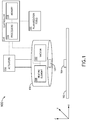
FIG. 1 illustrates a simplified block diagram view of asystem 100 for attaching semiconductor die to a die-attach preform, in accordance with one or more embodiments of the present disclosure. Thesystem 100 may include, but is not limited to, a formingsubstrate 102, ahandling tool 106, one ormore actuators 112, acontroller 114 including one ormore processors 116 and amemory 118. In another embodiment, thesystem 100 may include and one ormore planarization tools 122 communicatively coupled to thecontroller 114. - In embodiments, one or more die-attach
preforms 104 may be formed on the formingsubstrate 102. It is noted herein that the one or more die-attachpreforms 104 may be formed with any material known in the art including, but not limited to, sintered silver. In this regard, the one or more die-attachpreforms 104 may be referred to as sintered silver preforms 104. However, this is not to be regarded as a limitation of the present disclosure, unless noted otherwise herein. - The
handling tool 106 may be communicatively coupled to one ormore actuators 112 and/or thecontroller 114. For example, thehandling tool 106 may include one ormore heating elements 108 and one ormore vacuum sources 110 communicatively coupled to thecontroller 114. - In other embodiments, the
controller 114 may include one ormore processors 116 and amemory 118, wherein the one ormore processors 116 are configured to execute a set of program instructions stored inmemory 118, the set of program instructions configured to cause the one ormore processors 116 to carry out various steps/functions of the present disclosure. For example, the one ormore processors 116 may be configured to: generate one or more control signals configured to cause the one ormore planarization tools 122 to perform one or more planarization processes on the sintered silver preforms 104; generate one or more control signals configured to cause the one ormore actuators 112 to actuate thehandling tool 106 to couple thehandling tool 106 to one or more semiconductor die 120; generate one or more control signals configured to cause the one ormore vacuum sources 110 to create a suction force to handle the one or more semiconductor dies 120; generate one or more control signals configured to actuate thehandling tool 106 in order to bond the semiconductor die 120 to one or more sintered silver preforms 104; generate one or more control signals configured to cause the one ormore heating elements 108 to generate heat to cure the sintered silver preforms 104; and generate one or more control signals configured to cause the one ormore actuators 112 to actuate the semiconductor die 120 including asintered silver preform 104 in order to couple the semiconductor die 120 to a product substrate (not shown). - Each of the processes/functions carried out by the
controller 114 and other components ofsystem 100 may be further understood with reference toFIG. 2 . -
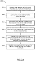
FIG. 2A illustrates a flowchart of a portion of amethod 200 for attaching semiconductor die 120 to a die-attachpreform 104, in accordance with one or more embodiments of the present disclosure. - In a
step 202, one or more die-attach preforms 104 (e.g., sintered silver preforms 104) are formed on a formingsubstrate 102. As noted previously herein, the die-attach material used to form the one or more die-attachpreforms 104 may include any die-attach material known in the art including, but not limited to, sintered silver, gold-tin eutectic materials, and the like. - The one or more die-attach
preforms 104 may be fabricated, printed, or otherwise formed using any technique known in the art. In embodiments, the one or more die-attachpreforms 104 may be formed by applying uncured (e.g., wet) die-attach material paste (e.g., sintered silver paste material) to the formingsubstrate 102. For example, a stencil may be disposed on a surface of the formingsubstrate 102, and a wet sintered silver paste material may be applied over the stencil and formingsubstrate 102. Subsequently, the stencil may be removed from the formingsubstrate 102. Upon removal of the stencil, excess sintered silver paste material may be removed, and the one or more sintered silver preforms 104 may be formed. It is noted herein that the stencil used to facilitate die-attachpreform 104 printing may exhibit varying shapes, sizes, and configurations. - The forming
substrate 102 may be formed from any material known in the art including, but not limited to, ceramic materials, alumina, and the like. It is contemplated herein that the use of a mechanically hard material, such as alumina, may reduce edge rounding in subsequent steps ofmethod 200 when the semiconductor die 120 is coupled to the die-attachpreforms 104. In embodiments, the formingsubstrate 102 may be configured and/or be formed from materials which facilitate removal/release of the die-attachpreforms 104 from the formingsubstrate 102. For example, the formingsubstrate 102 may be formed from and/or coated with a hydrophobic material in order to provide a non-stick surface to prevent the uncured (e.g., wet) die-attach material (e.g., sintered silver) from adhering to the formingsubstrate 102. For instance, the formingsubstrate 102 may be coated with a Teflon coating or other fluoropolymer coating. The hydrophobic coating used to provide a non-stick surface of the formingsubstrate 102 may be 1-2 µm thick. It is further noted herein that the use of a non-stick surface may provide a large contact angle on the formingsubstrate 102 in order to prevent the uncured (e.g., wet) die attach material from wetting underneath a stencil and/or flowing outside the borders of cut-outs within the stencil. - It is contemplated herein that the one or more die-attach
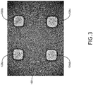
preforms 104 may be formed in any configuration or array known in the art. This may be further understood with reference toFIG. 3 . -
FIG. 3 illustrates a top view ofsintered silver preforms - As shown in
FIG. 3 , the one or more die-attach preforms 104 (e.g., sintered silver preforms 104) may be formed on the formingsubstrate 102 in a 2x2 array. For example, a stencil including cut-outs for a 2x2 array of preforms may be disposed on the formingsubstrate 102, applied with a wet sintered silver paste material, and subsequently removed to form the 2x2 array ofsintered silver preforms - In addition to enabling more efficient and reliable fabrication of semiconductor die 120 with die-attach layers, it has also been found that embodiments of the present disclosure may provide significant cost savings throughout the fabrication processes. Due to the fact that the die-attach
preforms 104 may be tailored to conform to specific sizes and shapes of specified semiconductor die 120, less die-attach material may be wasted, thereby decreasing the quantity of die-attach material required for a specified number of semiconductor dies 120. For example, it has been found that sintered silver preforms 104 may be formed at a cost of approximately $0.0005 perpreform 104/semiconductor die 120, significantly less than is feasible using traditional die-attach film approaches. - Reference will again be made to
FIG. 2A . In astep 204, the one or more die-attach preforms 104 (e.g., sintered silver preforms 104) are cured (e.g., dried). Curing the die-attachpreforms 104 may include heating and/or drying in order to form a solid, weakly-bonded material. For example, thecontroller 114 may be configured to generate one or more control signals configured to cause theheating elements 108 and/or heating elements external to the handling tool 106 (not shown) to generate heat in order to dry the sintered silver preforms 104. It is noted herein that the duration and/or temperature of the curing/drying process may be dependent upon the material used to form the die-attachpreforms 104. For example, the die-attachpreforms 104 may be cured at (e.g., dried) a temperature between 120-160°C below the sintering temperature associated with the die-attach material. For example, sintered silver preforms 104 may exhibit a sintering temperature between 250-290°C. In this regard, the sintered silver preforms 104 may be cured at a temperature of approximately 120-170°C. For instance, the sintered silver preforms 104 may be cured at a temperature of approximately 130°C. - In a
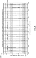
step 206, one or more planarization processes are performed on the one or more die-attach preforms 104 (e.g., sintered silver preforms 104). It is noted herein that, following curing instep 204, the die-attachpreforms 104 may typically exhibit a non-uniform thickness. This may be further understood with reference toFIG. 4 . -
FIG. 4 illustrates agraph 400 depicting thicknesses ofsintered silver preforms 104a-104f on a Teflon-coated formingsubstrate 102 prior to planarization, in accordance with one or more embodiments of the present disclosure. In particular,graph 400 illustrates the non-uniform thicknesses of a plurality ofsintered silver preforms 104a-104f fabricated on a Teflon-coated formingsubstrate 102. It is further noted herein, however, thatgraph 400 may also be understood to illustrate thicknesses ofsintered silver preforms 104a-104f on alternative and/or additional substrate surfaces configured to inhibit adhesion to thesubstrate 102. - As may be seen in
graph 400, each individualsintered silver preform 104a-104f may exhibit substantial thickness fluctuations across the upper surface of thesintered silver preform 104a-104f. Absent any planarization processes configured to level and flatten the surfaces of thesintered silver preforms 104a-104f, thesintered silver preforms 104a-104f would not be flush and/or conform to the surface of asemiconductor die 120, and would therefore may not form an adequate bond with the semiconductor die 120. - In this regard, one or more planarization processes may be performed in
step 206 in order to planarize the one or more die-attach preforms 104 (e.g., sinteredsilver preforms 104a-104f). The planarization processes may be configured to remove material from the die-attach preforms 104 (e.g., sinteredsilver preforms 104a-104f) in order to generate die-attachpreforms 104 of substantially uniform thicknesses. For example, thecontroller 114 may be configured to generate one or more control signals configured to cause the one ormore planarization tools 122 to perform one or more planarization processes on the die-attachpreforms 104 disposed on the formingsubstrate 102. Theplanarization tools 122 may include any planarization/machining tools known in the art including, but not limited to, precision lathes, precision mills, diamond turning machining tools, and the like. -
FIG. 5 illustrates agraph 500 depicting thicknesses of sintered silver preforms 104a-104e on a Teflon-coated formingsubstrate 102 following planarization, in accordance with one or more embodiments of the present disclosure. As may be seen ingraph 500, thesintered silver preforms 104a-104f may exhibit substantially improved thickness uniformity following planarization, which may enable effective coupling to the semiconductor die 120 in subsequent steps. It is further noted herein, however, thatgraph 500 may also be understood to illustrate thicknesses of sintered silver preforms 104a-104e on alternative and/or additional substrate surfaces configured to inhibit adhesion to thesubstrate 102. - Reference will again be made to
FIG. 2A . In astep 208, a first surface of asemiconductor die 120 is coupled to ahandling tool 106. For example, as shown inFIG. 1 , an upper surface of the semiconductor die 120 may be coupled to a lower surface of thehandling tool 106 such that thehandling tool 106 may be actuated and control the motion of the semiconductor die 120. - It is contemplated herein that the semiconductor die 120 may be held and/or coupled to the
handling tool 106 using any technique known in the art. For example, thesemiconductor substrate 120 may be coupled to thehandling tool 106 through the use of a graphite pad, vacuum suction, and the like. This may be further understood with reference toFIG. 2B . -
FIG. 2B illustrates a flowchart of a portion ofmethod 200 for fabricating semiconductor die 120 with a die-attach preform, in accordance with one or more embodiments of the present disclosure. In particular,FIG. 2B illustrates potential sub-steps ofstep 208 for coupling asemiconductor die 120 to ahandling tool 120. As noted previously herein, the semiconductor die 120 may be held and/or coupled to thehandling tool 106 using any technique known in the art. In this regard, the steps illustrated inFIG. 2B are provided as examples and are not to be regarded as a limitation of the present disclosure, unless noted otherwise herein. - In a
step 210, a graphite pad is formed on a surface of thehandling tool 106. Thehandling tool 106 may include any actuatable tool known in the art configured to receive and handle semiconductor materials including, but not limited to, a robot, an actuatable mechanical arm, and the like. This may be further shown and described with reference toFIGS. 6A-6B . -
FIG. 6A illustrates a bottom perspective view of ahandling tool 106, in accordance with one or more embodiments of the present disclosure.FIG. 6B illustrates a side perspective view of ahandling tool 106, in accordance with one or more embodiments of the present disclosure. - In embodiments, a
graphite pad 126 may be formed on asurface 124 of thehandling tool 106. For example, agraphite pad 126 may be formed on alower surface 124 of thehandling tool 106. Thesurface 124 of thehandling tool 106 may be formed from any material known in the art including, but not limited to, copper materials. Additionally, as noted previously herein with respect to the formingsubstrate 102, thesurface 124 of thehandling tool 106 configured to be coupled to thegraphite pad 126/semiconductor die 120 may be coated with a non-stick, hydrophobic coating (e.g., fluoropolymer coating, Teflon). Hydrophobic coatings on thesurface 124 of thehandling tool 106 may enable easier removal of thegraphite pad 126 and/orsemiconductor substrates 120 in subsequent steps. - The
graphite pad 126 may include any graphite pad known in the art including, but not limited to, a pyrolytic graphite film. In embodiments, agraphite pad 126 may be fabricated by applying a metal material to a graphite sheet. For example, after cleaning a graphite sheet (e.g., pyrolytic graphite sheet), the graphite sheet may be sputtered with an adhesion metal (e.g., titanium (Ti), chromium (Cr), nickel-chromium (NiCr)) followed by a seed metal(s) (e.g., palladium (Pd), copper (Cu)) and a low-melting temperature metal (e.g., tin (Sn), indium (In)). The various materials may be applied to the graphite sheet using any technique known in the art including, but not limited to, electroplating, electroless or immersion plating, sputtering, and the like. In embodiments,graphite pad 126 may be sized such that it substantially conforms to a shape and/or size of a selected semiconductor die 120. Any methods known in the art may be used to cut or otherwise shape thegraphite pad 126 including, but not limited to, steel rule die, razor blades, lasers, roll die, and the like. - In embodiments, the
graphite pad 126 may be subsequently coupled to thesurface 124 of thehandling tool 106. In some embodiments, thegraphite pad 126 may be coupled to thesurface 124 of thehandling tool 106 using one or more diffusion bonding processes. For example, thegraphite pad 126 may be coupled to thesurface 124 of thehandling tool 106 using transient liquid phase bonding, diffusion bonding, brazing processes, or the like. - For instance, in order to carry out transient liquid phase bonding, the
controller 114 may actuate thehandling tool 106 viaactuators 112 in order to bring thehandling tool 106 and thegraphite pad 126 into contact. Subsequently, thecontroller 114 may cause the one ormore heating elements 108 to generate heat and may actuate thehandling tool 106 in order to induce heat and pressure between thesurface 124 and thegraphite pad 126. While using tin as a metallizing material for thegraphite pad 126, the temperature for transient liquid phase bonding should be within the range of approximately 250°C and 350°C. Additionally, the bonding time required for transient liquid phase bonding may be dependent upon the materials used in forming thegraphite pad 126. A forming gas may be used during bonding in order to minimize oxidation of thecopper surface 124 of thehandling tool 106 and tin material within thegraphite pad 126. The resulting bond between thegraphite pad 126 andsurface 124 of thehandling tool 106 will be a high-melting point alloy/metallurgical bond with a melting point within the range of approximately 450°C and 550°C. It is noted herein that the creation of a high-melting point alloy to bond thegraphite pad 126 to thehandling tool 106 is important to ensure sintering temperatures of the die-attachpreforms 104 may be achieved without breaking the bond between thegraphite pad 126 to thehandling tool 106. Transient liquid phase bonding is described in further detail inU.S. Patent No. 7,830,021 B1, filed on September 6, 2005, naming Ross K. Wilcoxon, Alan P. Boone, and James R. Wooldridge as inventors which is incorporated herein by reference in the entirety. - In a
step 212, thegraphite pad 126 is coupled to a first surface of the semiconductor die 120. For example, thecontroller 114 may be configured to generate one or more control signals configured to cause theactuators 112 to actuate thehandling tool 106 in order to bring thesurface 124 and/orgraphite pad 126 into contact with an upper surface of asemiconductor die 120. - It is noted herein that the
graphite pad 126 may provide a soft but compliant surface which may prevent damage (e.g., scratching, cracking, passivation) to the semiconductor die 120. In particular, the compliancy of thegraphite pad 126 may help to evenly distribute pressure and bonding forces across the upper surface of the semiconductor die 120, which may reduce stress across the semiconductor die 120 and prevent damage to delicate chip features on the upper surface of the semiconductor die 120 (e.g., air bridges, PIN diodes, monolithic microwave integrated circuits (MMICs)). It is noted herein that thegraphite pad 126 may provide an efficient pick tool surface for a wide range of semiconductor die 120 sizes. - Additionally, the
graphite pad 126 may be configured to handle very high temperature bonding (e.g., greater than 500°C) and improve heat transfer to/through the semiconductor die 120 from the one ormore heating elements 108, which is necessary for high-speed bonding processes throughout subsequent steps ofmethod 200. Furthermore, as a good high-temperature elastomer, thegraphite pad 126 may be extremely resilient and capable of being heated and/or compressed many times without degrading. Accordingly, it is contemplated herein that thegraphite pad 126 may be used to handle many semiconductor die 120 throughout a fabrication process. Subsequently, when thegraphite pad 126 is to be removed, it has been found that thegraphite pad 126 may be easily removed from thesurface 124 of thehandling tool 106 via polishing processes. - In embodiments, the
graphite pad 126 may include one or more carve-outs configured to receive one or more structures disposed on the first surface (e.g., upper surface) of the semiconductor die 120. For example, the semiconductor die 120 may include any number of structures and/or features on the upper surface of the semiconductor die 120 (e.g., air bridges, PIN diodes, monolithic microwave integrated circuits (MMICs)). In order to reduce and/or prevent pressure from being applied to these structures, and potentially damaging the structures, one or more carve-outs may be formed in the bottom surface of thegraphite pad 126. The one or more carve-outs may be formed using any technique known in the art including, but not limited to, steel rule die, razor blades, lasers, roll die, and the like. Accordingly, the one or more carve-outs on the lower surface of thegraphite pad 126 may be configured to receive the one or more structures on the upper surface of the semiconductor die 120 in order to reduce and/or prevent pressure on the one or more structures. - In a
step 214, a suction force is applied through avacuum port 128 disposed in thesurface 124 of thehandling tool 106 with the one ormore vacuum sources 110. For example, thecontroller 114 may generate one or more control signals configured to cause the one ormore vacuum sources 110 to generate a suction force through avacuum port 128 disposed in thesurface 124 of thehandling tool 106. In this regard, the one ormore vacuum sources 110 may be fluidically coupled to thevacuum port 128 via one ormore lines 130. One ormore vacuum ports 128 may be distributed throughout thesurface 124 of thehandling tool 106. Thevacuum ports 128 may take on any shape or size. For example, the one ormore vacuum ports 128 may include circular ports with 3 mm diameters. - It is noted herein that suction forces may be used to temporarily couple a
semiconductor die 120 to thehandling tool 106. The suction forces may be used in addition to, or in lieu of, thegraphite pad 126 to enable efficient and reliable handling. In embodiments where thehandling tool 106 utilizes both agraphite pad 126 and suction forces to handle asemiconductor die 120, the suction forces may be applied through both thevacuum port 128 and thegraphite pad 126. For example, agraphite pad 126 may be formed on thesurface 124 of thehandling tool 106 such that thegraphite pad 126 completely or partially covers the one ormore vacuum ports 128. A drill or other means may then be used to remove the portions of thegraphite pad 126 covering the one ormore vacuum ports 128 in order to create one or more apertures within thegraphite pad 126. The one ormore vacuum sources 110 may then apply a suction force through the one ormore vacuum ports 128 and the one or more apertures within thegraphite pad 126. - In a
step 216, the first surface of the semiconductor die 120 is coupled to thehandling tool 106 and/orgraphite pad 126 via the suction force. For example, in embodiments without agraphite pad 126, a suction force may be applied through the one ormore vacuum ports 128 in order to couple thesurface 124 of thehandling tool 106 directly to the upper surface of the semiconductor die 120. By way of another example, in embodiments with agraphite pad 126, a suction force may be applied through the one ormore vacuum ports 128 and the one or more apertures within thegraphite pad 126 in order to couple a surface of thegraphite pad 126 to the upper surface of the semiconductor die 120. - Reference will again be made to
FIG. 2A . In astep 218, a second surface of the semiconductor die 120 is bonded to at least one die-attach preform 104 (e.g., sintered silver preform 104). For example, thecontroller 114 may generate one or more control signals configured to cause theactuators 112 to actuate thehandling tool 106 in order to bring the lower surface of the semiconductor die 120 into contact with an upper surface of asintered silver preform 104. In this regard, thehandling tool 106 may apply a first pressure between thegraphite pad 126 and the upper surface of the semiconductor die 120, and a second pressure between the lower surface of the semiconductor die 120 and the upper surface of asintered silver preform 104. - In a
step 220, the semiconductor die 120 including a bondedsintered silver preform 104 is bonded to a product substrate. For example, the semiconductor die 120 including asintered silver preform 104 bonded to the second surface of the semiconductor die 120 may be bonded to a product substrate 120 (e.g., printed circuit board (PCB), ceramic substrate, integrated circuit device, multi-chip module, and the like) using heat and pressure. - Using conventional techniques for coupling semiconductor die to die-attach films, large forces/pressures were required to be applied to the semiconductor die in order to cut the die-attach films. Conversely, due to the fact that the die-attach
preforms 104 are already cut and sized, the forces required to couple the semiconductor die 120 to the die-attachpreforms 104 may be significantly reduced, thereby preventing damage (e.g., scratching, cracking, passivation) to the semiconductor die 120. These reduced forces are especially important in the context of semiconductor die 120 with delicate structures (e.g., air bridges, PIN diodes, monolithic microwave integrated circuits (MMICs)) which are susceptible to damage under stress. Furthermore, it is noted herein that the area of small die is not linearly proportional to the perimeter. In this regard, conventional methods for cutting die-attach films require exceedingly high forces to achieve effective cutting of the die-attach films, which may damage the small semiconductor die 120. Accordingly, the reduced forces enabled by the present disclosure may prove to be extremely valuable in the context of enabling semiconductor die 120 of decreasing sizes. - It is noted herein that bonding with die-attach materials often requires pressure and heat. Accordingly, in some embodiments, the
controller 114 may generate one or more control signals configured to cause the one ormore heating elements 108 to generate heat such that heat may be applied through thesurface 124 of thehandling tool 106 and through thegraphite pad 126/semiconductor die 120 to the joint surface between the semiconductor die 120 and sinteredsilver preform 104. As noted previously herein, the temperature required for bonding the lower surface of the semiconductor die 120 and the upper surface of the die-attachpreform 104 may depend on the material of the die-attachpreform 104. For example, in embodiments with asintered silver preform 104, thecontroller 114 may cause theheating elements 108 to generate heat sufficient to raise the temperature of thesintered silver preform 104 to between 230°C and 300°C in order to bond the semiconductor die 120 to thesintered silver preform 104. - Following bonding of a die-attach preform 104 (e.g., sintered silver preform 104), the semiconductor die 120 may be coupled to a product substrate. A product substrate may include any product substrate configured to receive a
semiconductor die 120 including, but not limited to, a ceramic substrate, a printed circuit board (PCB), an integrated circuit, a package body (e.g., quad flat no-lead (QFN) package), and the like. For example, thecontroller 114 may generate one or more control signals configured to cause theactuators 112 to actuate thehandling tool 106 in order to bring a lower surface of the die-attachpreform 104 coupled to the semiconductor die 120 into contact with an upper surface of a product substrate. Thecontroller 114 may then generate one or more control signals configured to cause the one ormore heating elements 108 to generate heat such that heat may be applied through thesurface 124 of thehandling tool 106,graphite pad 126, semiconductor die 120, and die-attachpreform 104 to the joint surface between the die-attachpreform 104 and a surface of the product substrate. In this regard, theheating elements 108 may be used to sinter the die-attachpreform 104 coupled to asemiconductor die 120 in order to couple the semiconductor die 120 to the product substrate. - In embodiments, the use of the
handling tool 106 for handling the various components of the present disclosure may provide for improved precision tooling, flexible size options, and fabrication of high-density product substrates. In particular, the use of ahandling tool 106 actuatable via acontroller 114 may enable die-attachpreforms 104 and semiconductor die 120 to be fabricated and/or disposed adjacent to one another, thereby enabling further miniaturization of product substrates. - Embodiments of the present disclosure are directed to a novel die-attach material, process, and tooling approach for optimal thermal and RF performance of semiconductor die 120. As compared to conventional approaches, it is contemplated herein that the
system 100 andmethod 200 of the present disclosure may enable significant improvements in automation speed and throughput, as well as improvements in performance, yield, component miniaturization, and overall cost. - It is noted herein that the one or more components of
system 100 may be communicatively coupled to the various other components ofsystem 100 in any manner known in the art. For example, the one ormore processors 116 may be communicatively coupled to each other and other components via a wireline (e.g., copper wire, fiber optic cable, and the like) or wireless connection (e.g., RF coupling, IR coupling, data network communication (e.g., WiFi, WiMax, Bluetooth, 3G, 4G, 4G LTE, 5G and the like). - In one embodiment, the one or
more processors 116 may include any one or more processing elements known in the art. In this sense, the one ormore processors 116 may include any microprocessor-type device configured to execute software algorithms and/or instructions. In one embodiment, the one ormore processors 116 may consist of a desktop computer, mainframe computer system, workstation, image computer, parallel processor, or other computer system (e.g., networked computer) configured to execute a program configured to operate thesystem 100, as described throughout the present disclosure. It should be recognized that the steps described throughout the present disclosure may be carried out by a single computer system or, alternatively, multiple computer systems. Furthermore, it should be recognized that the steps described throughout the present disclosure may be carried out on any one or more of the one ormore processors 116. In general, the term "processor" may be broadly defined to encompass any device having one or more processing elements, which execute program instructions frommemory 118. Moreover, different subsystems of the system 100 (e.g.,controller 114,actuators 112,planarization tools 122, handling tool 106) may include processor or logic elements suitable for carrying out at least a portion of the steps described throughout the present disclosure. Therefore, the above description should not be interpreted as a limitation on the present disclosure but merely an illustration. - The
memory 118 may include any storage medium known in the art suitable for storing program instructions executable by the associated one ormore processors 116. For example, thememory 118 may include a non-transitory memory medium. For instance, thememory 118 may include, but is not limited to, a read-only memory (ROM), a random-access memory (RAM), a magnetic or optical memory device (e.g., disk), a magnetic tape, a solid-state drive and the like. It is further noted thatmemory 118 may be housed in a common controller housing with the one ormore processors 116. In an alternative embodiment, thememory 118 may be located remotely with respect to the physical location of theprocessors 116,controller 114, and the like. In another embodiment, thememory 118 maintains program instructions for causing the one ormore processors 116 to carry out the various steps described through the present disclosure. - It is to be understood that embodiments of the methods disclosed herein may include one or more of the steps described herein. Further, such steps may be carried out in any desired order and two or more of the steps may be carried out simultaneously with one another. Two or more of the steps disclosed herein may be combined in a single step, and in some embodiments, one or more of the steps may be carried out as two or more sub-steps. Further, other steps or sub-steps may be carried in addition to, or as substitutes to one or more of the steps disclosed herein.
- Although inventive concepts have been described with reference to the embodiments illustrated in the attached drawing figures, equivalents may be employed and substitutions made herein without departing from the scope of the claims. Components illustrated and described herein are merely examples of a system/device and components that may be used to implement embodiments of the inventive concepts and may be replaced with other devices and components without departing from the scope of the claims. Furthermore, any dimensions, degrees, and/or numerical ranges provided herein are to be understood as non-limiting examples unless otherwise specified in the claims.
Claims (15)
- A method for fabricating semiconductor die with die-attach preforms, comprising:applying an uncured die-attach paste material to a surface of a forming substrate to form one or more die-attach preforms, the surface of the forming substrate formed from a hydrophobic material;curing the one or more die-attach preforms;performing one or more planarization processes on the one or more die-attach preforms;coupling a first surface of a semiconductor die to a handling tool; andbonding a second surface of the semiconductor die to at least one die-attach preform of the one or more die-attach preforms.
- The method of Claim 1, wherein the one or more die-attach preforms comprise one or more sintered silver preforms.
- The method of Claims 1 or 2, wherein bonding the second surface of the semiconductor die to at least one die-attach preform comprises:
applying heat to the at least one die-attach preform with one or more heating elements disposed within the handling tool. - The method of any preceding Claim, further comprising:
coupling the semiconductor die to a product substrate by bonding the die-attach preform to the product substrate. - The method of Claim 4, wherein coupling the semiconductor die to a product substrate by bonding the die-attach preform to the product substrate comprises:
applying heat to the at least one die-attach preform bonded to the second surface of the semiconductor die with one or more heating elements disposed within the handling tool. - The method of any preceding Claim, wherein the one or more planarization processes are performed by at least one of a precision lathe, a precision mill, or a diamond turning machining tool.
- The method of any preceding Claim, wherein the at least one die-attach preform substantially conforms to a shape and size of the second surface of the semiconductor die.
- The method of any preceding Claim, wherein applying an uncured die-attach paste material to a forming substrate to form one or more die-attach preforms comprises:disposing a stencil on a forming substrate;applying an uncured die-attach paste material on top of the stencil; andremoving the stencil to form one or more die-attach preforms.
- The method of any preceding Claim, wherein coupling the first surface of the semiconductor die to the handling tool comprises:applying a suction force through a vacuum port disposed in a surface of the handling tool with one or more vacuum sources; andcoupling the first surface of the semiconductor die to the handling tool via the suction force.
- The method of Claim 1, wherein coupling the first surface of the semiconductor die to the handling tool comprises:forming a graphite pad on a surface of the handling tool; andcoupling the graphite pad to a first surface of the semiconductor die.
- The method of Claim 10, wherein the graphite pad includes one or more carve-outs, wherein coupling the graphite pad to a first surface of the semiconductor die comprises:
coupling the graphite pad to the first surface of the semiconductor die such that the one or more carve-outs of the graphite pad receive one or more structures disposed on the first surface of the semiconductor die. - The method of Claims 10 or 11, wherein bonding a second surface of the semiconductor die to at least one of the one or more die-attach preforms comprises:
actuating the handling tool to apply a first pressure between the graphite pad and the first surface of the semiconductor die, and to apply a second pressure between the second surface of the semiconductor die and the at least one die-attach preform. - The method of any of Claims 10-12, wherein forming a graphite pad on a surface of the actuatable handling tool comprises:applying a metal material to a graphite sheet to form a graphite pad; anddiffusion bonding the graphite pad to the surface of the actuatable handling tool.
- The method of any of Claims 10-13, wherein coupling the graphite pad to the first surface of the semiconductor die comprises:forming the graphite pad on the surface of the actuatable handling tool, wherein the graphite pad covers at least one portion of a vacuum port disposed in a surface of the actuatable handling tool;removing a portion of the graphite pad which covers the at least one portion of the vacuum port to create one or more apertures within the graphite pad;applying a suction force through the vacuum port and through the one or more apertures of the graphite pad with one or more vacuum sources; andcoupling the first surface of the semiconductor die to the handling tool via the suction force.
- A method for fabricating semiconductor die with die-attach preforms, comprising:forming one or more die-attach preforms on a forming substrate;performing one or more planarization processes on the one or more die-attach preforms;forming a graphite pad on a surface of a handling tool;coupling the graphite pad to a first surface of a semiconductor die; andbonding a second surface of the semiconductor die to at least one die-attach preform of the one or more die-attach preforms, wherein the at least one die-attach preform substantially conforms to a shape and size of the second surface of the semiconductor die.
Applications Claiming Priority (1)
| Application Number | Priority Date | Filing Date | Title |
|---|---|---|---|
| US16/530,016 US11373976B2 (en) | 2019-08-02 | 2019-08-02 | System and method for extreme performance die attach |
Publications (2)
| Publication Number | Publication Date |
|---|---|
| EP3772088A2 true EP3772088A2 (en) | 2021-02-03 |
| EP3772088A3 EP3772088A3 (en) | 2021-05-12 |
Family
ID=71948424
Family Applications (1)
| Application Number | Title | Priority Date | Filing Date |
|---|---|---|---|
| EP20189191.8A Pending EP3772088A3 (en) | 2019-08-02 | 2020-08-03 | Method for die attach using planarized die-attach preforms |
Country Status (2)
| Country | Link |
|---|---|
| US (1) | US11373976B2 (en) |
| EP (1) | EP3772088A3 (en) |
Cited By (1)
| Publication number | Priority date | Publication date | Assignee | Title |
|---|---|---|---|---|
| US11764185B2 (en) | 2021-08-31 | 2023-09-19 | Infineon Technologies Austria Ag | Diffusion soldering preform with varying surface profile |
Citations (1)
| Publication number | Priority date | Publication date | Assignee | Title |
|---|---|---|---|---|
| US7830021B1 (en) | 2005-09-06 | 2010-11-09 | Rockwell Collins, Inc. | Tamper resistant packaging with transient liquid phase bonding |
Family Cites Families (12)
| Publication number | Priority date | Publication date | Assignee | Title |
|---|---|---|---|---|
| DE3777995D1 (en) * | 1986-12-22 | 1992-05-07 | Siemens Ag | METHOD FOR FASTENING ELECTRONIC COMPONENTS ON A SUBSTRATE, FILM FOR IMPLEMENTING THE METHOD, AND METHOD FOR PRODUCING THE FILM. |
| US6875636B2 (en) * | 2003-07-14 | 2005-04-05 | Delphi Technologies, Inc. | Wafer applied thermally conductive interposer |
| WO2008096648A1 (en) * | 2007-02-09 | 2008-08-14 | Nippon Mining & Metals Co., Ltd. | Target formed of sintering-resistant material of high-melting point metal alloy, high-melting point metal silicide, high-melting point metal carbide, high-melting point metal nitride, or high-melting point metal boride, process for producing the target, assembly of the sputtering target-backing plate, and process for produc |
| DE102009018541A1 (en) * | 2009-04-24 | 2010-10-28 | W.C. Heraeus Gmbh | Contacting unit for electronic component, is porous metallic layered structure, and contact surface of electronic component and layered structure geometrically fit to each other, where thickness of layer is ten micrometers |
| US8716864B2 (en) * | 2012-06-07 | 2014-05-06 | Ixys Corporation | Solderless die attach to a direct bonded aluminum substrate |
| US9099567B2 (en) * | 2013-11-25 | 2015-08-04 | Freescale Semiconductor, Inc. | Packaged semiconductor devices and methods of their fabrication |
| MX2016012036A (en) * | 2014-05-05 | 2017-01-19 | Heraeus Deutschland Gmbh & Co Kg | METHOD FOR APPLYING A DRY METAL SINTERIZATION PREPARATION THROUGH A TRANSFER SUBSTRATE ON A SUBSTRATE FOR ELECTRONIC COMPONENTS, CORRESPONDING SUBSTRATE AND ITS USE FOR THE CONNECTION SINTERED TO ELECTRONIC COMPONENTS. |
| EP3154729A4 (en) * | 2014-06-12 | 2018-02-28 | Alpha Metals, Inc. | Sintering materials and attachment methods using same |
| DE102014111744B4 (en) * | 2014-08-18 | 2022-01-05 | Infineon Technologies Ag | ASSEMBLY FOR HANDLING A SEMICONDUCTOR CHIP AND METHOD OF HANDLING A SEMICONDUCTOR CHIP |
| DE102014117020A1 (en) * | 2014-11-20 | 2016-05-25 | Infineon Technologies Ag | METHOD FOR PRODUCING A CONNECTIVE CONNECTION BETWEEN A SEMICONDUCTOR CHIP AND A METAL LAYER |
| EP3587020A4 (en) * | 2017-02-23 | 2020-01-01 | Osaka University | ASSEMBLY ELEMENT, METHOD FOR PRODUCING AN ASSEMBLY ELEMENT, AND METHOD FOR PRODUCING AN ASSEMBLED STRUCTURE |
| JP7252798B2 (en) * | 2019-03-15 | 2023-04-05 | 日東電工株式会社 | Sheet for sinter bonding and sheet for sinter bonding with substrate |
-
2019
- 2019-08-02 US US16/530,016 patent/US11373976B2/en active Active
-
2020
- 2020-08-03 EP EP20189191.8A patent/EP3772088A3/en active Pending
Patent Citations (1)
| Publication number | Priority date | Publication date | Assignee | Title |
|---|---|---|---|---|
| US7830021B1 (en) | 2005-09-06 | 2010-11-09 | Rockwell Collins, Inc. | Tamper resistant packaging with transient liquid phase bonding |
Cited By (1)
| Publication number | Priority date | Publication date | Assignee | Title |
|---|---|---|---|---|
| US11764185B2 (en) | 2021-08-31 | 2023-09-19 | Infineon Technologies Austria Ag | Diffusion soldering preform with varying surface profile |
Also Published As
| Publication number | Publication date |
|---|---|
| US20210202433A1 (en) | 2021-07-01 |
| EP3772088A3 (en) | 2021-05-12 |
| US11373976B2 (en) | 2022-06-28 |
Similar Documents
| Publication | Publication Date | Title |
|---|---|---|
| JP7489956B2 (en) | Sintered material and bonding method using same | |
| KR102305501B1 (en) | Sintering materials and attachment methods using same | |
| JP5955392B2 (en) | Method for forming a connection portion used for bonding with a large diameter wire or strip between a metal molded body and a power semiconductor | |
| EP3772088A2 (en) | Method for die attach using planarized die-attach preforms | |
| KR20170030542A (en) | Method for producing a substrate adapter, substrate adapter, and method for contacting a semiconductor element | |
| CN107851632B (en) | Method for manufacturing a semiconductor device and corresponding device | |
| KR20030094026A (en) | Bonding Stage | |
| WO2021157470A1 (en) | Cutting device, bonding material transfer device, and mounting device | |
| KR102434064B1 (en) | Ceramic Board Manufacturing Method | |
| US11440310B2 (en) | Method for producing a substrate adapter and substrate adapter for connecting to an electronic component | |
| JP2002280705A (en) | Method of forming circuit on composite substrate and composite substrate | |
| JP2005166936A (en) | Method of forming die | |
| KR20240139062A (en) | Method for joining electrical and mechanical components using laminated modular preforms | |
| CN113140465A (en) | Direct bonded copper substrate manufactured using silver sintering | |
| JP7814521B2 (en) | Method for joining electrical and mechanical components using laminated modular preforms | |
| JP2005236112A (en) | Manufacturing method of semiconductor device | |
| CN217239420U (en) | Chip carrying device and system | |
| JP2021086911A (en) | Manufacturing method for device, joint device, and semiconductor device | |
| KR20210007253A (en) | Heat dissipating substrate and method of manufacturing the same | |
| JP2007005366A (en) | Method of manufacturing semiconductor device | |
| JPH0424188B2 (en) | ||
| JP2003048209A (en) | Manufacturing method of ceramic chip |
Legal Events
| Date | Code | Title | Description |
|---|---|---|---|
| PUAI | Public reference made under article 153(3) epc to a published international application that has entered the european phase |
Free format text: ORIGINAL CODE: 0009012 |
|
| STAA | Information on the status of an ep patent application or granted ep patent |
Free format text: STATUS: THE APPLICATION HAS BEEN PUBLISHED |
|
| AK | Designated contracting states |
Kind code of ref document: A2 Designated state(s): AL AT BE BG CH CY CZ DE DK EE ES FI FR GB GR HR HU IE IS IT LI LT LU LV MC MK MT NL NO PL PT RO RS SE SI SK SM TR |
|
| AX | Request for extension of the european patent |
Extension state: BA ME |
|
| PUAL | Search report despatched |
Free format text: ORIGINAL CODE: 0009013 |
|
| AK | Designated contracting states |
Kind code of ref document: A3 Designated state(s): AL AT BE BG CH CY CZ DE DK EE ES FI FR GB GR HR HU IE IS IT LI LT LU LV MC MK MT NL NO PL PT RO RS SE SI SK SM TR |
|
| RIC1 | Information provided on ipc code assigned before grant |
Ipc: H01L 21/60 20060101AFI20210407BHEP Ipc: H01L 21/67 20060101ALI20210407BHEP |
|
| STAA | Information on the status of an ep patent application or granted ep patent |
Free format text: STATUS: REQUEST FOR EXAMINATION WAS MADE |
|
| 17P | Request for examination filed |
Effective date: 20211108 |
|
| RBV | Designated contracting states (corrected) |
Designated state(s): AL AT BE BG CH CY CZ DE DK EE ES FI FR GB GR HR HU IE IS IT LI LT LU LV MC MK MT NL NO PL PT RO RS SE SI SK SM TR |
|
| STAA | Information on the status of an ep patent application or granted ep patent |
Free format text: STATUS: EXAMINATION IS IN PROGRESS |
|
| 17Q | First examination report despatched |
Effective date: 20250211 |