EP3767828B1 - Mehrphasenfilter - Google Patents
Mehrphasenfilter Download PDFInfo
- Publication number
- EP3767828B1 EP3767828B1 EP18915138.4A EP18915138A EP3767828B1 EP 3767828 B1 EP3767828 B1 EP 3767828B1 EP 18915138 A EP18915138 A EP 18915138A EP 3767828 B1 EP3767828 B1 EP 3767828B1
- Authority
- EP
- European Patent Office
- Prior art keywords
- resistor
- connection point
- reactance element
- capacitor
- output terminal
- Prior art date
- Legal status (The legal status is an assumption and is not a legal conclusion. Google has not performed a legal analysis and makes no representation as to the accuracy of the status listed.)
- Active
Links
Images


Classifications
-
- H—ELECTRICITY
- H03—ELECTRONIC CIRCUITRY
- H03H—IMPEDANCE NETWORKS, e.g. RESONANT CIRCUITS; RESONATORS
- H03H7/00—Multiple-port networks comprising only passive electrical elements as network components
- H03H7/18—Networks for phase shifting
- H03H7/21—Networks for phase shifting providing two or more phase shifted output signals, e.g. n-phase output
-
- H—ELECTRICITY
- H03—ELECTRONIC CIRCUITRY
- H03H—IMPEDANCE NETWORKS, e.g. RESONANT CIRCUITS; RESONATORS
- H03H11/00—Networks using active elements
- H03H11/02—Multiple-port networks
- H03H11/04—Frequency selective two-port networks
-
- H—ELECTRICITY
- H03—ELECTRONIC CIRCUITRY
- H03H—IMPEDANCE NETWORKS, e.g. RESONANT CIRCUITS; RESONATORS
- H03H7/00—Multiple-port networks comprising only passive electrical elements as network components
- H03H7/01—Frequency selective two-port networks
- H03H7/06—Frequency selective two-port networks including resistors
Definitions
- the present invention relates to an RC polyphase filter.
- An RC polyphase filter is available as a polyphase filter.
- resistors R and capacitors C are alternately connected together in series in a ring shape and a circuit is formed with four resistors and four capacitors, and first and second input terminals and first to fourth output terminals are included (for example, see Patent Literature 1).
- a predetermined frequency is differentially input to the first input terminal and the second input terminal, and a predetermined frequency of a quadrature differential is output from the first to fourth output terminals.
- Patent Literature 1 JP 2013-509096 A
- US 4123712 A relates to a symmetrical polyphase R-C network, in which each section has a resistor serially connected between its input and output and a capacitor connected between the input of one section and the output of an adjacent section.
- the network has a second resistor connected in shunt with the output of each section to decrease the passband ripple of the network with negligible effect on the stopband response.
- US 4326109 A relates to apparatus for coupling a two-way transmission path to a one-way transmitting path and a one-way receiving path.
- the apparatus comprises: a first phase-shift network having an input and two outputs at which a signal supplied to said input is produced in phase quadrature; a second phase-shift network having two inputs, which are connected to the outputs of the first phase-shift network, and an output, the second phase-shift network being conjugate to the first whereby a signal applied to the input of the first network and produced in phase quadrature at the outputs of the first network is not produced at the output of the second network; and means for connecting the two-way transmission path to one of the outputs of the first network, a balancing impedance to the other of the outputs of the first network, the one-way transmitting path to the output of the second network and the one-way receiving path to the input of the first network.
- US 3618133 A relates to a symmetrical polyphase network including constant reactances such that the symmetrical polyphase network responds differently to input signals of negative and positive frequencies, wherein four-phase constrained network comprises a transistor in each phase.
- US 2014/0312989 A1 relates to poly-phase filter, which receives inphase input signals and quadrature input signals, and provides inphase output signals and quadrature output signals.
- SHAILESH KULKARNI ET AL Design of an Optimal Layout Polyphase Filter for Millimeter-Wave Quadrature LO Generation " relates to the analysis and design of a two-stage passive RC polyphase filter for millimeter-wave quadrature local oscillator generation.
- polyphase filter there are two input feeding structures for quadrature generation, wherein one type has a constant amplitude, and another type has a constant phase.
- US 2011/092169A1 relates an LR polyphaser filter implemented with inductors and resistors and capable of operating at high frequencies.
- the LR polyphase filter may include first and second paths.
- the first path may include a first inductor coupled to a first resistor and may receive a first input signal and provide a first output signal.
- the second path may include a second inductor coupled to a second resistor and may receive the first input signal and provide a second output signal.
- the conventional polyphase filter has an asymmetric circuit configuration, voltages and currents output to the first to fourth output terminals are unbalanced, and there has been a problem that variations in impedance occurs, and an amplitude error or a phase error occurs.
- the present invention has been made to solve the problem as described above, and an object thereof is to provide a polyphase filter that can obtain an output in which the variations in impedance, the amplitude error, and the phase error are suppressed.
- the four resistors and the four reactance elements are alternately connected together in series to form the circuit in the ring shape
- the first to fourth output terminals are connected to the series connection points between the first to fourth resistors and the first to fourth reactance elements
- the first input terminal is connected to the series connection point between the fourth reactance element and the first resistor
- the second input terminal is connected to the series connection point between the second reactance element and the third resistor.
- the fifth resistor is connected between the series connection point between the first reactance element and the second resistor and the series connection point between the third reactance element and the fourth resistor.
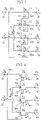
- FIG. 1 is a configuration diagram illustrating a polyphase filter according to a present embodiment.
- resistors and capacitors that are reactance elements are alternately connected together in series to form a circuit in a ring shape, and input terminals and output terminals are included at connection points between the resistors and the capacitors.
- a first resistor 11, a second resistor 12, a third resistor 13, a fourth resistor 14, a fifth resistor 15, a first capacitor 21, a second capacitor 22, a third capacitor 23, a fourth capacitor 24, a first input terminal 31, a second input terminal 32, a first output terminal 41, a second output terminal 42, a third output terminal 43, and a fourth output terminal 44 are included.
- the ring shape here does not indicate only a circle, but also includes a shape with corners (an arrangement shape including the first resistor 11, the first capacitor 21, the second resistor 12, the second capacitor 22, the third resistor 13, the third capacitor 23, the fourth resistor 14, and the fourth capacitor 24 in FIG. 1 ).
- the first input terminal 31 is connected to a series connection point 101 between the first resistor 11 and the fourth capacitor 24, and the second input terminal 32 is connected to a series connection point 103 between the third resistor 13 and the second capacitor 22.
- the first output terminal 41 is connected to a series connection point 201 between the first resistor 11 and the first capacitor 21, the second output terminal 42 is connected to a series connection point 202 between the second resistor 12 and the second capacitor 22, the third output terminal 43 is connected to a series connection point 203 between the third resistor 13 and the third capacitor 23, and the fourth output terminal 44 is connected to a series connection point 204 between the fourth resistor 14 and the fourth capacitor 24.
- One end of the fifth resistor 15 is connected to a series connection point 102 between the first capacitor 21 and the second resistor 12, and the other end of the fifth resistor 15 is connected to a series connection point 104 between the third capacitor 23 and the fourth resistor 14.
- An absolute value of an impedance of each of the first resistor 11 to the fourth resistor 14 and the first capacitor 21 to the fourth capacitor 24 is the same as an impedance of the first input terminal 31 at a predetermined frequency.
- a radio wave input from the first input terminal 31 is input to the series connection point 101 between the first resistor 11 and the fourth capacitor 24, and a radio wave input from the second input terminal 32, having a differential relationship with the radio wave input from the first input terminal 31, is input to the series connection point 103 between the third resistor 13 and the second capacitor 22.
- I i1 represents an input current of the first input terminal 31
- I i3 represents an input current of the second input terminal 32
- V i1 represents an input voltage of the first input terminal
- V i3 represents an input voltage of the second input terminal 32.
- the first output terminal 41 is connected to the second output terminal 42 through the first capacitor 21, the second output terminal 42 is connected to the third output terminal 43 through the second capacitor 22, the third output terminal 43 is connected to the fourth output terminal 44 through the third capacitor 23, and the fourth output terminal 44 is connected to the first output terminal 41 through the fourth capacitor 24, so that outputs of the output terminals 41, 42, 43, and 44 differ in phase by 90 degrees each.
- the resistor between the capacitor and the output terminal does not contribute to the amount of phase shift.
- quadrature differential outputs for example, 0°, -90°, -180°, -270°
- I R1 represents a current flowing through the first resistor 11, and V o1 and I ⁇ 1 represent an output voltage and an output current of the first output terminal 41.
- I R2 represents a current flowing through the second resistor 12
- V o2 and I o2 represent an output voltage and an output current of the second output terminal 42
- I R3 represents a current flowing through the third resistor 13
- V o3 and I o3 represent an output voltage and an output current of the third output terminal 43
- I R4 represents a current flowing through the fourth resistor 14
- V o4 and I o4 represent an output voltage and an output current of the fourth output terminal 44.
- I C1 to I C4 respectively represent currents flowing through the first capacitor 21 to the fourth capacitor 24, V i2 and V i4 respectively represent voltages at the series connection point 102 and the series connection point 104, and I R5 represents a current flowing through the fifth resistor 15.
- the current I C4 flowing through the fourth capacitor 24 merges with the current I i1 flowing through the first input terminal 31 and flows through the first resistor 11, and the current I R1 flowing through the first resistor 11 is distributed to the first output terminal 41 and the first capacitor 21.
- the current I C1 flowing through the first capacitor 21 merges with the current I R5 flowing through the fifth resistor 15 and flows through the second resistor 12, and the current I R2 flowing through the second resistor 12 is distributed to the second output terminal 42 and the second capacitor 22.
- the current I R2 flowing through the second resistor 12 includes only the current I C1 ( ⁇ I R1 ) flowing through the first capacitor 21, and is not a current balanced with the current I R1 flowing through the first resistor 11.
- the current I C2 flowing through the second capacitor 22 is distributed to the current I i3 flowing through the second input terminal 32 (in a reverse-phase relationship with the first input terminal 31) and the third resistor 13, and the current I R3 flowing through the third resistor 13 is distributed to the third output terminal 43 and the third capacitor 23.
- the current I C3 flowing through the third capacitor 23 is distributed to the fifth resistor 15 and the fourth resistor 14, and the current I R4 flowing through the fourth resistor 14 is distributed to the fourth output terminal 44 and the fourth capacitor 24.
- the current I R4 flowing through the fourth resistor 14 includes only the current Ic3 ( ⁇ I R3 ) flowing through the third capacitor 23, and is not a current balanced with the current I R3 flowing through the third resistor 13.
- the impedance is the ratio between the voltage and the current
- a good balance between the voltage and the current makes the impedances equal to each other, and can eliminate a deviation of the impedance matching.
- the voltage and the current are balanced with each other, the amplitude error and the phase error are suppressed.
- the amplitude error is a factor of the phase error when the vector composition is considered, suppressing the amplitude error also suppresses the phase error.
- resistance values of the first resistor 11 to the fourth resistor 14 are made equal to impedances of the first input terminal 31, the second input terminal 32, and the first output terminal 41 to the fourth output terminal 44, and a resistance value of the fifth resistor 15 is set to be twice the impedance of the first input terminal 31 (equal to a load impedance between the first input terminal 31 and the second input terminal 32 in absolute value), whereby, in principle, impedance matching can be achieved at all input and output terminals, and the amplitude error and the phase error can be made zero.
- the impedance between the first input terminal 31 and the second input terminal 32 is 100 ⁇
- the resistance values of the first output terminal 41 to the fourth output terminal 44 and the first resistor 11 to the fourth resistor 14 each are 50 ⁇
- the resistance value of the fifth resistor 15 is 100 ⁇ .
- the absolute value of the impedance of each of the first capacitor 21 to the fourth capacitor 24 is 50 ⁇ .
- the first resistor, the first reactance element, the second resistor, the second reactance element, the third resistor, the third reactance element, the fourth resistor, and the fourth reactance element are connected together in series in the ring shape
- the fifth resistor is connected between the series connection point between the first reactance element and the second resistor and the series connection point between the third reactance element and the fourth resistor
- the first output terminal is connected to the series connection point between the first resistor and the first reactance element
- the second output terminal is connected to the series connection point between the second resistor and the second reactance element
- the third output terminal is connected to the series connection point between the third resistor and the third reactance element
- the fourth output terminal is connected to the series connection point between the fourth resistor and the fourth reactance element
- the first input terminal is connected to the series connection point between the fourth reactance element and the first resistor
- the second input terminal is connected to the series connection point between the second reactance element and the third resistor
- the polyphase filter in one embodiment, since the first to fourth reactance elements may be capacitors, the polyphase filter can be easily implemented.
- the absolute value of the fifth resistor is equal to the absolute value of the impedance between the first input terminal and the second input terminal, so that impedance matching between the input and the output is perfectly achieved, the power loss due to the reflection can be suppressed, and the output can be obtained in which the amplitude error and the phase error are suppressed.
- FIG. 2 is a configuration diagram illustrating a polyphase filter according to a second embodiment.
- resistors and capacitors are alternately connected together in series to form a circuit in a ring shape, and input terminals and output terminals are included at connection points between the resistors and the capacitors, similarly to the first embodiment shown in FIG. 1 , but the method of connecting the resistors and the capacitors together is different.
- the first input terminal 31 is connected to a series connection point 301 between the first resistor 11 and the first capacitor 21, and the second input terminal 32 is connected to a series connection point 303 between the third resistor 13 and the third capacitor 23.
- the first output terminal 41 is connected to a series connection point 401 between the first resistor 11 and the fourth capacitor 24, the second output terminal 42 is connected to a series connection point 402 between the second resistor 12 and the first capacitor 21, the third output terminal 43 is connected to a series connection point 403 between the third resistor 13 and the second capacitor 22, and the fourth output terminal 44 is connected to a series connection point 404 between the fourth resistor 14 and the third capacitor 23.
- one end of the fifth resistor 15 is connected to a series connection point 302 between the second capacitor 22 and the second resistor 12, and the other end of the fifth resistor 15 is connected to a series connection point 304 between the fourth capacitor 24 and the fourth resistor 14.
- the absolute values of the impedances of the first resistor 11 to the fourth resistor 14 and the first capacitor 21 to the fourth capacitor 24 are the same as the impedances of the first input terminal 31 and the second input terminal 32 at a predetermined frequency.
- the ring shape here does not indicate only a circle, but also includes a shape with corners (an arrangement shape including the first resistor 11, the first capacitor 21, the second resistor 12, the second capacitor 22, the third resistor 13, the third capacitor 23, the fourth resistor 14, and the fourth capacitor 24 in FIG. 2 ).
- a radio wave input from the first input terminal 31 is input to the series connection point 301 between the first resistor 11 and the first capacitor 21, and a radio wave input from the second input terminal 32, having a differential relationship with the radio wave input from the first input terminal 31, is input to the series connection point 303 between the third resistor 13 and the third capacitor 23.
- the first output terminal 41 is connected to the second output terminal 42 through the first capacitor 21, the second output terminal 42 is connected to the third output terminal 43 through the second capacitor 22, the third output terminal 43 is connected to the fourth output terminal 44 through the third capacitor 23, and the fourth output terminal 44 is connected to the first output terminal 41 through the fourth capacitor 24.
- the outputs of the output terminals 41, 42, 43, and 44 differ in phase by 90 degrees each.
- the resistor between the capacitor and the output terminal does not contribute to the amount of phase shift.
- quadrature differential outputs for example, 0°, -90°, -180°, -270°
- the current flowing through the first capacitor 21 is merged with the current flowing through the first input terminal 31 and flows through the first resistor 11, and the current flowing through the first resistor 11 is distributed to the first output terminal 41 and the fourth capacitor 24.
- the current flowing through the second capacitor 22 is merged with the current flowing through the fifth resistor 15 and flows through the second resistor 12, and the current flowing through the second resistor 12 is distributed to the second output terminal 42 and the first capacitor 21.
- the current flowing through the second resistor 12 includes only the current flowing through the second capacitor 22, and is not a current balanced with the current flowing through the first resistor 11.
- the current flowing through the third capacitor 23 is distributed to the current flowing through the second input terminal 32 (in a reverse-phase relationship with the first input terminal 31) and the third resistor 13, and the current flowing through the third resistor 13 is distributed to the third output terminal 43 and the second capacitor 22.
- the current flowing through the fourth capacitor 24 is distributed to the fifth resistor 15 and the fourth resistor 14, and the current flowing through the fourth resistor 14 is distributed to the fourth output terminal 44 and the third capacitor 23.
- the current flowing through the fourth resistor 14 includes only the current flowing through the fourth capacitor 24, and is not a current balanced with the current flowing through the third resistor 13.
- the impedance is the ratio between the voltage and the current
- a good balance between the voltage and the current makes the impedances equal to each other, and can eliminate a deviation of the impedance matching.
- the voltage and the current are balanced with each other, the amplitude error and the phase error are suppressed.
- the amplitude error is a factor of the phase error when the vector composition is considered, suppressing the amplitude error also suppresses the phase error.
- resistance values of the first resistor 11 to the fourth resistor 14 are made equal to impedances of the first input terminal 31, the second input terminal 32, and the first output terminal 41 to the fourth output terminal 44, and a resistance value of the fifth resistor 15 is set to be twice the impedance of the first input terminal 31 (equal to a load impedance between the first input terminal 31 and the second input terminal 32), whereby, in principle, impedance matching can be achieved at all input and output terminals, and the amplitude error and the phase error can be made zero.
- the impedance between the first input terminal 31 and the second input terminal 32 is 100 ⁇
- the resistance values of the first output terminal 41 to the fourth output terminal 44 and the first resistor 11 to the fourth resistor 14 each are 50 ⁇
- the resistance value of the fifth resistor 15 is 100 ⁇ .
- the absolute value of the impedance of each of the first capacitor 21 to the fourth capacitor 24 is 50 ⁇ .
- the first resistor, the first reactance element, the second resistor, the second reactance element, the third resistor, the third reactance element, the fourth resistor, and the fourth reactance element are connected together in series in the ring shape
- the fifth resistor is connected between the series connection point between the second resistor and the second reactance element and the series connection point between the fourth resistor and the fourth reactance element
- the first output terminal is connected to the series connection point between the fourth reactance element and the first resistor
- the second output terminal is connected to the series connection point between the first reactance element and the second resistor
- the third output terminal is connected to the series connection point between the second reactance element and the third resistor
- the fourth output terminal is connected to the series connection point between the third reactance element and the fourth resistor
- the first input terminal is connected to the series connection point between the first resistor and the first reactance element
- the second input terminal is connected to the series connection point between the third resistor and the third reactance element, so that variations in im
- a third embodiment is an example in which the first capacitor 21 to the fourth capacitor 24 are replaced with inductors.
- FIG. 3 illustrates a configuration of a polyphase filter according to the third embodiment.
- the first capacitor 21 is replaced with a first inductor 61
- the second capacitor 22 is replaced with a second inductor 62
- the third capacitor 23 is replaced with a third inductor 63
- the fourth capacitor 24 is replaced with a fourth inductor 64.
- the series connection point 101 in the first embodiment corresponds to a series connection point 501
- the series connection point 102 corresponds to a series connection point 502
- the series connection point 103 corresponds to a series connection point 503
- the series connection point 104 corresponds to a series connection point 504.
- the series connection point 201 in the first embodiment corresponds to a series connection point 601
- the series connection point 202 corresponds to a series connection point 602
- the series connection point 203 corresponds to a series connection point 603
- the series connection point 204 corresponds to a series connection point 604.
- I L1 to I L4 represent currents flowing through the first inductor 61 to the fourth inductor 64, respectively.
- the basic operation is similar to that of the polyphase filter according to the first embodiment.
- the difference is that the phases of the capacitor and the inductor are opposite to each other, and a phase relationship among output waves from the first output terminal 41 to the fourth output terminal 44 is, for example, 0°, 90°, 180°, 270°. From these, by providing the fifth resistor 15, a highly symmetrical voltage-current relationship is formed, the variations in impedance can be suppressed, and the amplitude error and the phase error are suppressed.
- resistance values of the first resistor 11 to the fourth resistor 14 are made equal to those of the first input terminal 31, the second input terminal 32, and the first output terminal 41 to the fourth output terminal 44, and a resistance value of the fifth resistor 15 is set to be twice the impedance of the first input terminal 31 (equal to a load impedance between the first input terminal 31 and the second input terminal 32), whereby, in principle, impedance matching can be achieved at all input and output terminals, and the amplitude error and the phase error can be made zero.
- first inductor 61 to the fourth inductors 64 may be replaced with transmission lines having a length of 1/4 wavelength at a predetermined frequency.
- the polyphase filter of the third embodiment since the first to fourth reactance elements are inductors, the polyphase filter can be easily implemented.
- the polyphase filter of the third embodiment since the first to fourth reactance elements are transmission lines, the polyphase filter can be easily implemented.
- a fourth embodiment is an example in which the first resistor 11 to the fourth resistor 14 and the first capacitor 21 to the fourth capacitor 24 are replaced with drain-source resistances and gate-source capacitances of transistors.
- FIG. 4 illustrates a configuration of a polyphase filter according to the fourth embodiment.
- the polyphase filter according to the fourth embodiment includes a first transistor 71 to a fourth transistor 74.
- the first input terminal 31 is connected to a connection point 701 between the drain terminal of the first transistor 71 and the gate terminal of the fourth transistor 74
- the second input terminal 32 is connected to a connection point 703 between the drain terminal of the third transistor 73 and the gate terminal of the second transistor 72.
- the first output terminal 41 is connected to the source terminal of the first transistor 71
- the second output terminal 42 is connected to the source terminal of the second transistor 72
- the third output terminal 43 is connected to the source terminal of the third transistor 73
- the fourth output terminal 44 is connected to the source terminal of the fourth transistor 74.
- the gate terminal of the first transistor 71 and the drain terminal of the second transistor 72 are connected together at a connection point 702, and the gate terminal of the third transistor 73 and the drain terminal of the fourth transistor 74 are connected together at a connection point 704. Then, the fifth resistor 15 is connected between the connection point 702 and the connection point 704.
- FIG. 5 is a basic equivalent circuit of the transistor.
- the transistor has a resistance Rds and a mutual conductance gm between the drain and the source, and a capacitance Cgs between the gate and the source.
- Rds resistance
- Cgs capacitance
- a radio wave input from the first input terminal 31 is input to the connection point 701 between the drain terminal of the first transistor 71 and the gate terminal of the fourth transistor 74, and a radio wave input from the second input terminal 32, having a differential relationship with the radio wave input from the first input terminal 31, is input to the connection point 703 between the drain terminal of the third transistor 73 and the gate terminal of the second transistor 72.
- the first output terminal 41 is connected to the second output terminal 42 through a gate-source capacitance of the first transistor 71
- the second output terminal 42 is connected to the third output terminal 43 through a gate-source capacitance of the second transistor 72
- the third output terminal 43 is connected to the fourth output terminal 44 through a gate-source capacitance of the third transistor 73
- the fourth output terminal 44 is connected to the first output terminal 41 through a gate-source capacitance of the fourth transistor 74.
- a current flowing through the gate-source capacitance of the fourth transistor 74 is merged with the current flowing through the first input terminal 31 and flows through the drain-source resistance of the first transistor 71, and the current flowing through the drain-source resistance of the first transistor 71 is distributed to the first output terminal 41 and the gate-source capacitance of the first transistor 71.
- a current flowing through the gate-source capacitance of the first transistor 71 is merged with the current flowing through the fifth resistor 15 and flows through the drain-source resistance of the second transistor 72, and the current flowing through the drain-source resistance of the second transistor 72 is distributed to the second output terminal 42 and the gate-source capacitance of the second transistor 72.
- the current flowing through the drain-source resistance of the second transistor 72 includes only the current flowing through the gate-source capacitance of the first transistor 71, and is not a current balanced with the current flowing through the drain-source resistance of the first transistor 71.
- a current flowing through the gate-source capacitance of the second transistor 72 is distributed to the current flowing through the second input terminal 32 (in a reverse-phase relationship with the first input terminal 31) and the drain-source resistance of the third transistor 73, and a current flowing through the drain-source resistance of the third transistor 73 is distributed to the third output terminal 43 and the gate-source capacitance of the third transistor 73.
- a current flowing through the gate-source capacitance of the third transistor 73 is distributed to the fifth resistor 15 and the drain-source resistance of the fourth transistor 74, and the current flowing through the drain-source resistance of the fourth transistor 74 is distributed to the fourth output terminal 44 and the gate-source capacitance of the fourth transistor 74.
- the current flowing through the drain-source resistance of the fourth transistor 74 is equal to the current flowing through the gate-source capacitance of the third transistor 73, and is not a current balanced with the current flowing through the drain-source resistance of the third transistor 73.
- values of the drain-source resistances of the first transistor 71 to the fourth transistor 74 are made equal to the impedance between the first input terminal 31 and the second input terminal 32 and the impedances of the first output terminal 41 to the fourth output terminal 44, and a resistance value of the fifth resistor 15 is set to be twice the impedance of the first input terminal 31 (equal to a load impedance between the first input terminal 31 and the second input terminal 32), whereby, in principle, impedance matching can be achieved at all input and output terminals, and the amplitude error and the phase error can be made zero.
- a resistor may be loaded in parallel with the drain-source resistance of the transistor, and a capacitor may be loaded in parallel with the gate-source capacitance of the transistor.
- amplification action of the transistor since the amplification action of the transistor is not used in the fourth embodiment, it is not necessary to apply a DC voltage to the transistor. However, a DC voltage may be applied to the transistor to control the mutual conductance, the gate-source capacitance, and the like.
- the first to fourth resistors are the drain-source resistances of the transistors
- the first to fourth reactance elements are the gate-source capacitances of the transistors, so that variations in impedance can be suppressed, and the output can be obtained in which the amplitude error and the phase error are suppressed.
- the polyphase filter according to the present invention relates to the configuration of the RC polyphase filter and is suitable for use in a high frequency circuit.
Landscapes
- Networks Using Active Elements (AREA)
Claims (7)
- Polyphasenfilter, aufweisend erste und zweite Eingangsanschlüsse (31, 32) zum Empfangen eines Eingangssignals und erste bis vierte Ausgangsanschlüsse (41, 42, 43, 44) zum Ausgeben von vier Ausgangssignalen, die aus dem Eingangssignal erzeugt wurden, wobei die Ausgangssignale in der Phase voneinander verschieden sind, wobei das Filter erste bis fünfte Widerstände und erste bis vierte Reaktanzelemente umfasst, wobeiein Ende des ersten Widerstands (11) mit einem Ende des ersten Reaktanzelements (21) verbunden ist, das andere Ende des ersten Reaktanzelements (21) mit einem Ende des zweiten Widerstands (12) verbunden ist, das andere Ende des zweiten Widerstands (12) mit einem Ende des zweiten Reaktanzelements (22) verbunden ist, das andere Ende des zweiten Reaktanzelements (22) mit einem Ende des dritten Widerstands (13) verbunden ist, das andere Ende des dritten Widerstands (13) mit einem Ende des dritten Reaktanzelements (23) verbunden ist, das andere Ende des dritten Reaktanzelements (23) mit einem Ende des vierten Widerstands (14) verbunden ist, das andere Ende des vierten Widerstands (14) mit einem Ende des vierten Reaktanzelements (24) verbunden ist, das andere Ende des vierten Reaktanzelements (24) mit dem anderen Ende des ersten Widerstands (11) verbunden ist,ein Ende des fünften Widerstands (15) nur mit dem Verbindungspunkt zwischen dem ersten Reaktanzelement (21) und dem zweiten Widerstand (12) verbunden ist, und das andere Ende des fünften Widerstands (15) nur mit dem Verbindungspunkt zwischen dem dritten Reaktanzelement (23) und dem vierten Widerstand (14) verbunden ist,der erste Ausgangsanschluss (41) mit dem Verbindungspunkt (201) zwischen dem ersten Widerstand (11) und dem ersten Reaktanzelement (21) verbunden ist,der zweite Ausgangsanschluss (42) mit dem Verbindungspunkt (202) zwischen dem zweiten Widerstand (12) und dem zweiten Reaktanzelement (22) verbunden ist,der dritte Ausgangsanschluss (43) mit dem Verbindungspunkt (203) zwischen dem dritten Widerstand (13) und dem dritten Reaktanzelement (23) verbunden ist,der vierte Ausgangsanschluss (44) mit dem Verbindungspunkt (204) zwischen dem vierten Widerstand (14) und dem vierten Reaktanzelement (24) verbunden ist,nur der erste und zweite Eingangsanschluss (31, 32) Eingangsanschlüsse des Polyphasenfilters sind,der erste Eingangsanschluss (31) nur mit dem Verbindungspunkt zwischen dem vierten Reaktanzelement (24) und dem ersten Widerstand (11) verbunden ist,der zweite Eingangsanschluss (32) mit dem Verbindungspunkt zwischen dem zweiten Reaktanzelement (22) und dem dritten Widerstand (13) verbunden ist,
- Polyphasenfilter, aufweisend erste und zweite Eingangsanschlüsse (31, 32) zum Empfangen eines Eingangssignals und erste bis vierte Ausgangsanschlüsse (41, 42, 43, 44) zum Ausgeben von vier Ausgangssignalen, die aus dem Eingangssignal erzeugt wurden, wobei die Ausgangssignale in der Phase voneinander verschieden sind, wobei das Filter erste bis fünfte Widerstände und erste bis vierte Reaktanzelemente umfasst, wobeiein Ende des ersten Widerstands (11) mit einem Ende des ersten Reaktanzelements (21) verbunden ist, das andere Ende des ersten Reaktanzelements (21) mit einem Ende des zweiten Widerstands (12) verbunden ist, das andere Ende des zweiten Widerstands (12) mit einem Ende des zweiten Reaktanzelements (22) verbunden ist, das andere Ende des zweiten Reaktanzelements (22) mit einem Ende des dritten Widerstands (13) verbunden ist, das andere Ende des dritten Widerstands (13) mit einem Ende des dritten Reaktanzelements (23) verbunden ist, das andere Ende des dritten Reaktanzelements (23) mit dem einen Ende des vierten Widerstands (14) verbunden ist, das andere Ende des vierten Widerstands (14) mit einem Ende des vierten Reaktanzelements (24) verbunden ist, das andere Ende des vierten Reaktanzelements (24) mit dem anderen Ende des ersten Widerstands (11) verbunden ist,ein Ende eines fünften Widerstands (15) nur mit dem Verbindungspunkt zwischen dem zweiten Widerstand (12) und dem zweiten Reaktanzelement (22) verbunden ist, und das andere Ende des fünften Widerstands (15) nur mit dem Verbindungspunkt zwischen dem vierten Widerstand (14) und dem vierten Reaktanzelement (24) verbunden ist,der erste Ausgangsanschluss (41) mit dem Verbindungspunkt (401) zwischen dem vierten Reaktanzelement (24) und dem ersten Widerstand (11) verbunden ist,der zweite Ausgangsanschluss (42) mit dem Verbindungspunkt (402) zwischen dem ersten Reaktanzelement (21) und dem zweiten Widerstand (12) verbunden ist,der dritte Ausgangsanschluss (43) mit dem Verbindungspunkt (403) zwischen dem zweiten Reaktanzelement (22) und dem dritten Widerstand (13) verbunden ist,der vierte Ausgangsanschluss (44) mit dem Verbindungspunkt (404) zwischen dem dritten Reaktanzelement (23) und dem vierten Widerstand (14) verbunden ist,nur der erste und zweite Eingangsanschluss (31, 32) Eingangsanschlüsse des Polyphasenfilters sind,der erste Eingangsanschluss (31) nur mit dem Verbindungspunkt zwischen dem ersten Widerstand (11) und dem ersten Reaktanzelement (21) verbunden ist, undder zweite Eingangsanschluss (32) nur mit dem Verbindungspunkt zwischen dem dritten Widerstand (13) und dem dritten Reaktanzelement (23) verbunden ist.
- Polyphasenfilter nach Anspruch 1 oder 2, wobei die ersten bis vierten Reaktanzelemente Kondensatoren (21, 22, 23 und 24) sind.
- Polyphasenfilter nach Anspruch 1 oder 2, wobei die ersten bis vierten Reaktanzelemente Induktoren (61, 62, 63 und 64) sind.
- Polyphasenfilter nach Anspruch 1 oder 2, wobei das erste bis vierte Reaktanzelement Übertragungsleitungen sind.
- Polyphasenfilter nach Anspruch 1 oder 2, wobei der erste bis vierte Widerstand (11, 12, 13 und 14) Drain-Source-Widerstände von Transistoren sind, und das erste bis vierte Reaktanzelement (21, 22, 23 und 24) Gate-Source-Kapazitäten der Transistoren sind.
- Polyphasenfilter nach Anspruch 1 oder 2, wobei ein Absolutwert des fünften Widerstands (15) gleich einem Absolutwert einer Impedanz zwischen dem ersten Eingangsanschluss (31) und dem zweiten Eingangsanschluss (32) ist.
Applications Claiming Priority (1)
| Application Number | Priority Date | Filing Date | Title |
|---|---|---|---|
| PCT/JP2018/016015 WO2019202686A1 (ja) | 2018-04-18 | 2018-04-18 | ポリフェーズフィルタ |
Publications (3)
| Publication Number | Publication Date |
|---|---|
| EP3767828A4 EP3767828A4 (de) | 2021-01-20 |
| EP3767828A1 EP3767828A1 (de) | 2021-01-20 |
| EP3767828B1 true EP3767828B1 (de) | 2022-09-21 |
Family
ID=68240016
Family Applications (1)
| Application Number | Title | Priority Date | Filing Date |
|---|---|---|---|
| EP18915138.4A Active EP3767828B1 (de) | 2018-04-18 | 2018-04-18 | Mehrphasenfilter |
Country Status (5)
| Country | Link |
|---|---|
| US (1) | US11211919B2 (de) |
| EP (1) | EP3767828B1 (de) |
| JP (1) | JP6749521B2 (de) |
| CN (1) | CN111937301A (de) |
| WO (1) | WO2019202686A1 (de) |
Family Cites Families (25)
| Publication number | Priority date | Publication date | Assignee | Title |
|---|---|---|---|---|
| GB1174709A (en) * | 1968-06-07 | 1969-12-17 | Standard Telephones Cables Ltd | A Symmetrical Polyphase Network |
| US4123712A (en) * | 1977-04-22 | 1978-10-31 | Northern Telecom Limited | Symmetrical polyphase network |
| US4326109A (en) * | 1980-04-11 | 1982-04-20 | Northern Telecom Limited | Apparatus for coupling a two-way transmission path to a one-way transmitting path and a one-way receiving path |
| JPH0831772B2 (ja) | 1990-03-16 | 1996-03-27 | 日本電信電話株式会社 | 位相合成・分岐回路 |
| US5187457A (en) * | 1991-09-12 | 1993-02-16 | Eni Div. Of Astec America, Inc. | Harmonic and subharmonic filter |
| IN188829B (de) * | 1994-02-16 | 2002-11-09 | Indfos Ind Ltd | |
| US5942929A (en) * | 1997-05-22 | 1999-08-24 | Qualcomm Incorporated | Active phase splitter |
| JP2001313544A (ja) | 2000-04-20 | 2001-11-09 | Lucent Technol Inc | 位相発生器 |
| JP3595982B2 (ja) | 2000-07-12 | 2004-12-02 | 日本電信電話株式会社 | 90度ハイブリッド回路 |
| US7084823B2 (en) * | 2003-02-26 | 2006-08-01 | Skycross, Inc. | Integrated front end antenna |
| US7164901B2 (en) * | 2003-12-24 | 2007-01-16 | Agency For Science, Technology And Research | DC offset-free RF front-end circuits and systems for direct conversion receivers |
| JP4242353B2 (ja) * | 2004-02-04 | 2009-03-25 | パナソニック株式会社 | 半導体装置 |
| JP4689345B2 (ja) * | 2005-05-12 | 2011-05-25 | パナソニック株式会社 | 受動型ポリフェーズフィルタ |
| CN101329382A (zh) * | 2007-06-19 | 2008-12-24 | 上海蓝波高电压技术设备有限公司 | 用于交联电缆的高压无局放试验电源 |
| JP2009177463A (ja) * | 2008-01-24 | 2009-08-06 | Alps Electric Co Ltd | ポリフェーズフィルタ |
| US20120256704A1 (en) * | 2011-03-01 | 2012-10-11 | Greatbatch Ltd. | Rf filter for an active medical device (amd) for handling high rf power induced in an associated implanted lead from an external rf field |
| US8412141B2 (en) | 2009-10-19 | 2013-04-02 | Qualcomm Incorporated | LR polyphase filter |
| JP5565149B2 (ja) * | 2010-07-01 | 2014-08-06 | 富士電機株式会社 | 電力変換装置 |
| US9391010B2 (en) * | 2012-04-02 | 2016-07-12 | Taiwan Semiconductor Manufacturing Co., Ltd. | Power line filter for multidimensional integrated circuits |
| US9077307B2 (en) * | 2012-12-20 | 2015-07-07 | St-Ericsson Sa | Polyphase filter for MM-wave frequencies featuring symmetric layout |
| US9106202B2 (en) * | 2013-04-17 | 2015-08-11 | Linear Technology Corporation | Poly-phase filter with phase tuning |
| EP3228004B1 (de) * | 2014-12-02 | 2018-09-05 | Telefonaktiebolaget LM Ericsson (publ) | Quadratursignalgenerator, strahlformungsanordnung kommunikationsvorrichtung und basisstation |
| JP6078133B1 (ja) * | 2015-10-06 | 2017-02-08 | 日本電信電話株式会社 | 分布型回路 |
| EP3419166B1 (de) * | 2016-02-17 | 2020-01-01 | Mitsubishi Electric Corporation | Polyphasenfilter und filterschaltung |
| WO2018158902A1 (ja) * | 2017-03-02 | 2018-09-07 | 三菱電機株式会社 | ポリフェーズフィルタ |
-
2018
- 2018-04-18 EP EP18915138.4A patent/EP3767828B1/de active Active
- 2018-04-18 JP JP2020514847A patent/JP6749521B2/ja active Active
- 2018-04-18 WO PCT/JP2018/016015 patent/WO2019202686A1/ja not_active Ceased
- 2018-04-18 CN CN201880091988.3A patent/CN111937301A/zh active Pending
-
2020
- 2020-09-16 US US17/023,075 patent/US11211919B2/en active Active
Also Published As
| Publication number | Publication date |
|---|---|
| JP6749521B2 (ja) | 2020-09-02 |
| US11211919B2 (en) | 2021-12-28 |
| CN111937301A (zh) | 2020-11-13 |
| WO2019202686A1 (ja) | 2019-10-24 |
| JPWO2019202686A1 (ja) | 2020-08-06 |
| EP3767828A4 (de) | 2021-01-20 |
| US20200412339A1 (en) | 2020-12-31 |
| EP3767828A1 (de) | 2021-01-20 |
Similar Documents
| Publication | Publication Date | Title |
|---|---|---|
| KR101165485B1 (ko) | 균형 혼합기를 사용하는 장비 일체 | |
| US6696885B2 (en) | Polyphase filters in silicon integrated circuit technology | |
| US6831497B2 (en) | Active quadrature signal generator using load having low-pass and high-pass filter characteristics | |
| CN103329435A (zh) | 基带平衡-不平衡变换器的失衡检测和减小 | |
| US8330506B2 (en) | Frequency multiplier circuit | |
| US6952142B2 (en) | Frequency-selective balun transformer | |
| US8552782B1 (en) | Quadrature phase network | |
| JPH1032451A (ja) | 集中素子を有する受動結合器回路を含む装置 | |
| US6388543B1 (en) | System for eight-phase 45° polyphase filter with amplitude matching | |
| US5214796A (en) | Image separation mixer | |
| GB2529903A (en) | IQ signal generator system and method | |
| EP3767828B1 (de) | Mehrphasenfilter | |
| US8478220B2 (en) | Discrete time polyphase mixer | |
| CN1981429B (zh) | 使用配合的平衡混频器 | |
| US20040091053A1 (en) | Impedance-matched IQ network for an image rejection circuit | |
| EP3761507B1 (de) | Mehrphasenfilter | |
| JP2003008399A (ja) | 移相器 | |
| US20060252396A1 (en) | Phase generator using polyphase architecture | |
| WO2014086385A1 (en) | An i/q network | |
| JP2018011167A (ja) | 電圧制御発振器 | |
| US6714602B1 (en) | Demodulator and receiver | |
| JP2001257538A (ja) | 直交ミキサ回路及び複素ミキサ回路 | |
| Fabre et al. | Phase compensation of ideal inductances based second-generation current conveyors | |
| KR19990067078A (ko) | 동조제어방식 | |
| WO1996004712A1 (en) | Tuning amplifier |
Legal Events
| Date | Code | Title | Description |
|---|---|---|---|
| STAA | Information on the status of an ep patent application or granted ep patent |
Free format text: STATUS: THE INTERNATIONAL PUBLICATION HAS BEEN MADE |
|
| PUAI | Public reference made under article 153(3) epc to a published international application that has entered the european phase |
Free format text: ORIGINAL CODE: 0009012 |
|
| STAA | Information on the status of an ep patent application or granted ep patent |
Free format text: STATUS: REQUEST FOR EXAMINATION WAS MADE |
|
| 17P | Request for examination filed |
Effective date: 20201012 |
|
| A4 | Supplementary search report drawn up and despatched |
Effective date: 20201126 |
|
| AK | Designated contracting states |
Kind code of ref document: A1 Designated state(s): AL AT BE BG CH CY CZ DE DK EE ES FI FR GB GR HR HU IE IS IT LI LT LU LV MC MK MT NL NO PL PT RO RS SE SI SK SM TR |
|
| AX | Request for extension of the european patent |
Extension state: BA ME |
|
| DAV | Request for validation of the european patent (deleted) | ||
| DAX | Request for extension of the european patent (deleted) | ||
| STAA | Information on the status of an ep patent application or granted ep patent |
Free format text: STATUS: EXAMINATION IS IN PROGRESS |
|
| 17Q | First examination report despatched |
Effective date: 20210916 |
|
| GRAP | Despatch of communication of intention to grant a patent |
Free format text: ORIGINAL CODE: EPIDOSNIGR1 |
|
| STAA | Information on the status of an ep patent application or granted ep patent |
Free format text: STATUS: GRANT OF PATENT IS INTENDED |
|
| INTG | Intention to grant announced |
Effective date: 20220513 |
|
| GRAS | Grant fee paid |
Free format text: ORIGINAL CODE: EPIDOSNIGR3 |
|
| GRAA | (expected) grant |
Free format text: ORIGINAL CODE: 0009210 |
|
| STAA | Information on the status of an ep patent application or granted ep patent |
Free format text: STATUS: THE PATENT HAS BEEN GRANTED |
|
| AK | Designated contracting states |
Kind code of ref document: B1 Designated state(s): AL AT BE BG CH CY CZ DE DK EE ES FI FR GB GR HR HU IE IS IT LI LT LU LV MC MK MT NL NO PL PT RO RS SE SI SK SM TR |
|
| REG | Reference to a national code |
Ref country code: GB Ref legal event code: FG4D |
|
| REG | Reference to a national code |
Ref country code: CH Ref legal event code: EP |
|
| REG | Reference to a national code |
Ref country code: IE Ref legal event code: FG4D |
|
| REG | Reference to a national code |
Ref country code: DE Ref legal event code: R096 Ref document number: 602018041012 Country of ref document: DE |
|
| REG | Reference to a national code |
Ref country code: AT Ref legal event code: REF Ref document number: 1520470 Country of ref document: AT Kind code of ref document: T Effective date: 20221015 |
|
| REG | Reference to a national code |
Ref country code: LT Ref legal event code: MG9D |
|
| REG | Reference to a national code |
Ref country code: NL Ref legal event code: MP Effective date: 20220921 |
|
| PG25 | Lapsed in a contracting state [announced via postgrant information from national office to epo] |
Ref country code: SE Free format text: LAPSE BECAUSE OF FAILURE TO SUBMIT A TRANSLATION OF THE DESCRIPTION OR TO PAY THE FEE WITHIN THE PRESCRIBED TIME-LIMIT Effective date: 20220921 Ref country code: RS Free format text: LAPSE BECAUSE OF FAILURE TO SUBMIT A TRANSLATION OF THE DESCRIPTION OR TO PAY THE FEE WITHIN THE PRESCRIBED TIME-LIMIT Effective date: 20220921 Ref country code: NO Free format text: LAPSE BECAUSE OF FAILURE TO SUBMIT A TRANSLATION OF THE DESCRIPTION OR TO PAY THE FEE WITHIN THE PRESCRIBED TIME-LIMIT Effective date: 20221221 Ref country code: LV Free format text: LAPSE BECAUSE OF FAILURE TO SUBMIT A TRANSLATION OF THE DESCRIPTION OR TO PAY THE FEE WITHIN THE PRESCRIBED TIME-LIMIT Effective date: 20220921 Ref country code: LT Free format text: LAPSE BECAUSE OF FAILURE TO SUBMIT A TRANSLATION OF THE DESCRIPTION OR TO PAY THE FEE WITHIN THE PRESCRIBED TIME-LIMIT Effective date: 20220921 Ref country code: FI Free format text: LAPSE BECAUSE OF FAILURE TO SUBMIT A TRANSLATION OF THE DESCRIPTION OR TO PAY THE FEE WITHIN THE PRESCRIBED TIME-LIMIT Effective date: 20220921 |
|
| REG | Reference to a national code |
Ref country code: AT Ref legal event code: MK05 Ref document number: 1520470 Country of ref document: AT Kind code of ref document: T Effective date: 20220921 |
|
| PG25 | Lapsed in a contracting state [announced via postgrant information from national office to epo] |
Ref country code: HR Free format text: LAPSE BECAUSE OF FAILURE TO SUBMIT A TRANSLATION OF THE DESCRIPTION OR TO PAY THE FEE WITHIN THE PRESCRIBED TIME-LIMIT Effective date: 20220921 Ref country code: GR Free format text: LAPSE BECAUSE OF FAILURE TO SUBMIT A TRANSLATION OF THE DESCRIPTION OR TO PAY THE FEE WITHIN THE PRESCRIBED TIME-LIMIT Effective date: 20221222 |
|
| PG25 | Lapsed in a contracting state [announced via postgrant information from national office to epo] |
Ref country code: SM Free format text: LAPSE BECAUSE OF FAILURE TO SUBMIT A TRANSLATION OF THE DESCRIPTION OR TO PAY THE FEE WITHIN THE PRESCRIBED TIME-LIMIT Effective date: 20220921 Ref country code: RO Free format text: LAPSE BECAUSE OF FAILURE TO SUBMIT A TRANSLATION OF THE DESCRIPTION OR TO PAY THE FEE WITHIN THE PRESCRIBED TIME-LIMIT Effective date: 20220921 Ref country code: PT Free format text: LAPSE BECAUSE OF FAILURE TO SUBMIT A TRANSLATION OF THE DESCRIPTION OR TO PAY THE FEE WITHIN THE PRESCRIBED TIME-LIMIT Effective date: 20230123 Ref country code: ES Free format text: LAPSE BECAUSE OF FAILURE TO SUBMIT A TRANSLATION OF THE DESCRIPTION OR TO PAY THE FEE WITHIN THE PRESCRIBED TIME-LIMIT Effective date: 20220921 Ref country code: CZ Free format text: LAPSE BECAUSE OF FAILURE TO SUBMIT A TRANSLATION OF THE DESCRIPTION OR TO PAY THE FEE WITHIN THE PRESCRIBED TIME-LIMIT Effective date: 20220921 Ref country code: AT Free format text: LAPSE BECAUSE OF FAILURE TO SUBMIT A TRANSLATION OF THE DESCRIPTION OR TO PAY THE FEE WITHIN THE PRESCRIBED TIME-LIMIT Effective date: 20220921 |
|
| PG25 | Lapsed in a contracting state [announced via postgrant information from national office to epo] |
Ref country code: SK Free format text: LAPSE BECAUSE OF FAILURE TO SUBMIT A TRANSLATION OF THE DESCRIPTION OR TO PAY THE FEE WITHIN THE PRESCRIBED TIME-LIMIT Effective date: 20220921 Ref country code: PL Free format text: LAPSE BECAUSE OF FAILURE TO SUBMIT A TRANSLATION OF THE DESCRIPTION OR TO PAY THE FEE WITHIN THE PRESCRIBED TIME-LIMIT Effective date: 20220921 Ref country code: IS Free format text: LAPSE BECAUSE OF FAILURE TO SUBMIT A TRANSLATION OF THE DESCRIPTION OR TO PAY THE FEE WITHIN THE PRESCRIBED TIME-LIMIT Effective date: 20230121 Ref country code: EE Free format text: LAPSE BECAUSE OF FAILURE TO SUBMIT A TRANSLATION OF THE DESCRIPTION OR TO PAY THE FEE WITHIN THE PRESCRIBED TIME-LIMIT Effective date: 20220921 |
|
| P01 | Opt-out of the competence of the unified patent court (upc) registered |
Effective date: 20230512 |
|
| REG | Reference to a national code |
Ref country code: DE Ref legal event code: R097 Ref document number: 602018041012 Country of ref document: DE |
|
| PG25 | Lapsed in a contracting state [announced via postgrant information from national office to epo] |
Ref country code: NL Free format text: LAPSE BECAUSE OF FAILURE TO SUBMIT A TRANSLATION OF THE DESCRIPTION OR TO PAY THE FEE WITHIN THE PRESCRIBED TIME-LIMIT Effective date: 20220921 Ref country code: AL Free format text: LAPSE BECAUSE OF FAILURE TO SUBMIT A TRANSLATION OF THE DESCRIPTION OR TO PAY THE FEE WITHIN THE PRESCRIBED TIME-LIMIT Effective date: 20220921 |
|
| PLBE | No opposition filed within time limit |
Free format text: ORIGINAL CODE: 0009261 |
|
| STAA | Information on the status of an ep patent application or granted ep patent |
Free format text: STATUS: NO OPPOSITION FILED WITHIN TIME LIMIT |
|
| PG25 | Lapsed in a contracting state [announced via postgrant information from national office to epo] |
Ref country code: DK Free format text: LAPSE BECAUSE OF FAILURE TO SUBMIT A TRANSLATION OF THE DESCRIPTION OR TO PAY THE FEE WITHIN THE PRESCRIBED TIME-LIMIT Effective date: 20220921 |
|
| 26N | No opposition filed |
Effective date: 20230622 |
|
| PG25 | Lapsed in a contracting state [announced via postgrant information from national office to epo] |
Ref country code: SI Free format text: LAPSE BECAUSE OF FAILURE TO SUBMIT A TRANSLATION OF THE DESCRIPTION OR TO PAY THE FEE WITHIN THE PRESCRIBED TIME-LIMIT Effective date: 20220921 |
|
| REG | Reference to a national code |
Ref country code: CH Ref legal event code: PL |
|
| PG25 | Lapsed in a contracting state [announced via postgrant information from national office to epo] |
Ref country code: LU Free format text: LAPSE BECAUSE OF NON-PAYMENT OF DUE FEES Effective date: 20230418 |
|
| REG | Reference to a national code |
Ref country code: BE Ref legal event code: MM Effective date: 20230430 |
|
| PG25 | Lapsed in a contracting state [announced via postgrant information from national office to epo] |
Ref country code: MC Free format text: LAPSE BECAUSE OF FAILURE TO SUBMIT A TRANSLATION OF THE DESCRIPTION OR TO PAY THE FEE WITHIN THE PRESCRIBED TIME-LIMIT Effective date: 20220921 |
|
| PG25 | Lapsed in a contracting state [announced via postgrant information from national office to epo] |
Ref country code: MC Free format text: LAPSE BECAUSE OF FAILURE TO SUBMIT A TRANSLATION OF THE DESCRIPTION OR TO PAY THE FEE WITHIN THE PRESCRIBED TIME-LIMIT Effective date: 20220921 Ref country code: LI Free format text: LAPSE BECAUSE OF NON-PAYMENT OF DUE FEES Effective date: 20230430 Ref country code: CH Free format text: LAPSE BECAUSE OF NON-PAYMENT OF DUE FEES Effective date: 20230430 |
|
| REG | Reference to a national code |
Ref country code: IE Ref legal event code: MM4A |
|
| PG25 | Lapsed in a contracting state [announced via postgrant information from national office to epo] |
Ref country code: BE Free format text: LAPSE BECAUSE OF NON-PAYMENT OF DUE FEES Effective date: 20230430 |
|
| PG25 | Lapsed in a contracting state [announced via postgrant information from national office to epo] |
Ref country code: IE Free format text: LAPSE BECAUSE OF NON-PAYMENT OF DUE FEES Effective date: 20230418 |
|
| PG25 | Lapsed in a contracting state [announced via postgrant information from national office to epo] |
Ref country code: IE Free format text: LAPSE BECAUSE OF NON-PAYMENT OF DUE FEES Effective date: 20230418 |
|
| PG25 | Lapsed in a contracting state [announced via postgrant information from national office to epo] |
Ref country code: IT Free format text: LAPSE BECAUSE OF FAILURE TO SUBMIT A TRANSLATION OF THE DESCRIPTION OR TO PAY THE FEE WITHIN THE PRESCRIBED TIME-LIMIT Effective date: 20220921 |
|
| PG25 | Lapsed in a contracting state [announced via postgrant information from national office to epo] |
Ref country code: BG Free format text: LAPSE BECAUSE OF FAILURE TO SUBMIT A TRANSLATION OF THE DESCRIPTION OR TO PAY THE FEE WITHIN THE PRESCRIBED TIME-LIMIT Effective date: 20220921 |
|
| PG25 | Lapsed in a contracting state [announced via postgrant information from national office to epo] |
Ref country code: BG Free format text: LAPSE BECAUSE OF FAILURE TO SUBMIT A TRANSLATION OF THE DESCRIPTION OR TO PAY THE FEE WITHIN THE PRESCRIBED TIME-LIMIT Effective date: 20220921 |
|
| REG | Reference to a national code |
Ref country code: DE Ref legal event code: R084 Ref document number: 602018041012 Country of ref document: DE |
|
| PGFP | Annual fee paid to national office [announced via postgrant information from national office to epo] |
Ref country code: FR Payment date: 20250310 Year of fee payment: 8 |
|
| PGFP | Annual fee paid to national office [announced via postgrant information from national office to epo] |
Ref country code: GB Payment date: 20250227 Year of fee payment: 8 |
|
| PGFP | Annual fee paid to national office [announced via postgrant information from national office to epo] |
Ref country code: DE Payment date: 20250305 Year of fee payment: 8 |
|
| PG25 | Lapsed in a contracting state [announced via postgrant information from national office to epo] |
Ref country code: CY Free format text: LAPSE BECAUSE OF FAILURE TO SUBMIT A TRANSLATION OF THE DESCRIPTION OR TO PAY THE FEE WITHIN THE PRESCRIBED TIME-LIMIT; INVALID AB INITIO Effective date: 20180418 |
|
| PG25 | Lapsed in a contracting state [announced via postgrant information from national office to epo] |
Ref country code: HU Free format text: LAPSE BECAUSE OF FAILURE TO SUBMIT A TRANSLATION OF THE DESCRIPTION OR TO PAY THE FEE WITHIN THE PRESCRIBED TIME-LIMIT; INVALID AB INITIO Effective date: 20180418 |
|
| REG | Reference to a national code |
Ref country code: GB Ref legal event code: 746 Effective date: 20250805 |
|
| PG25 | Lapsed in a contracting state [announced via postgrant information from national office to epo] |
Ref country code: TR Free format text: LAPSE BECAUSE OF FAILURE TO SUBMIT A TRANSLATION OF THE DESCRIPTION OR TO PAY THE FEE WITHIN THE PRESCRIBED TIME-LIMIT Effective date: 20220921 |