EP3763796B1 - Electrical debonding type adhesive sheet, joined body, and joining and separation method for adherend - Google Patents
Electrical debonding type adhesive sheet, joined body, and joining and separation method for adherend Download PDFInfo
- Publication number
- EP3763796B1 EP3763796B1 EP19764294.5A EP19764294A EP3763796B1 EP 3763796 B1 EP3763796 B1 EP 3763796B1 EP 19764294 A EP19764294 A EP 19764294A EP 3763796 B1 EP3763796 B1 EP 3763796B1
- Authority
- EP
- European Patent Office
- Prior art keywords
- adherend
- adhesive layer
- adhesive sheet
- adhesive
- layer
- Prior art date
- Legal status (The legal status is an assumption and is not a legal conclusion. Google has not performed a legal analysis and makes no representation as to the accuracy of the status listed.)
- Active
Links
Images


Classifications
-
- C—CHEMISTRY; METALLURGY
- C09—DYES; PAINTS; POLISHES; NATURAL RESINS; ADHESIVES; COMPOSITIONS NOT OTHERWISE PROVIDED FOR; APPLICATIONS OF MATERIALS NOT OTHERWISE PROVIDED FOR
- C09J—ADHESIVES; NON-MECHANICAL ASPECTS OF ADHESIVE PROCESSES IN GENERAL; ADHESIVE PROCESSES NOT PROVIDED FOR ELSEWHERE; USE OF MATERIALS AS ADHESIVES
- C09J7/00—Adhesives in the form of films or foils
- C09J7/20—Adhesives in the form of films or foils characterised by their carriers
- C09J7/29—Laminated material
-
- B—PERFORMING OPERATIONS; TRANSPORTING
- B32—LAYERED PRODUCTS
- B32B—LAYERED PRODUCTS, i.e. PRODUCTS BUILT-UP OF STRATA OF FLAT OR NON-FLAT, e.g. CELLULAR OR HONEYCOMB, FORM
- B32B27/00—Layered products comprising a layer of synthetic resin
- B32B27/06—Layered products comprising a layer of synthetic resin as the main or only constituent of a layer, which is next to another layer of the same or of a different material
- B32B27/10—Layered products comprising a layer of synthetic resin as the main or only constituent of a layer, which is next to another layer of the same or of a different material of paper or cardboard
-
- B—PERFORMING OPERATIONS; TRANSPORTING
- B32—LAYERED PRODUCTS
- B32B—LAYERED PRODUCTS, i.e. PRODUCTS BUILT-UP OF STRATA OF FLAT OR NON-FLAT, e.g. CELLULAR OR HONEYCOMB, FORM
- B32B27/00—Layered products comprising a layer of synthetic resin
- B32B27/12—Layered products comprising a layer of synthetic resin next to a fibrous or filamentary layer
-
- B—PERFORMING OPERATIONS; TRANSPORTING
- B32—LAYERED PRODUCTS
- B32B—LAYERED PRODUCTS, i.e. PRODUCTS BUILT-UP OF STRATA OF FLAT OR NON-FLAT, e.g. CELLULAR OR HONEYCOMB, FORM
- B32B27/00—Layered products comprising a layer of synthetic resin
- B32B27/30—Layered products comprising a layer of synthetic resin comprising vinyl (co)polymers; comprising acrylic (co)polymers
- B32B27/308—Layered products comprising a layer of synthetic resin comprising vinyl (co)polymers; comprising acrylic (co)polymers comprising acrylic (co)polymers
-
- B—PERFORMING OPERATIONS; TRANSPORTING
- B32—LAYERED PRODUCTS
- B32B—LAYERED PRODUCTS, i.e. PRODUCTS BUILT-UP OF STRATA OF FLAT OR NON-FLAT, e.g. CELLULAR OR HONEYCOMB, FORM
- B32B27/00—Layered products comprising a layer of synthetic resin
- B32B27/36—Layered products comprising a layer of synthetic resin comprising polyesters
-
- B—PERFORMING OPERATIONS; TRANSPORTING
- B32—LAYERED PRODUCTS
- B32B—LAYERED PRODUCTS, i.e. PRODUCTS BUILT-UP OF STRATA OF FLAT OR NON-FLAT, e.g. CELLULAR OR HONEYCOMB, FORM
- B32B29/00—Layered products comprising a layer of paper or cardboard
- B32B29/02—Layered products comprising a layer of paper or cardboard next to a fibrous or filamentary layer
-
- B—PERFORMING OPERATIONS; TRANSPORTING
- B32—LAYERED PRODUCTS
- B32B—LAYERED PRODUCTS, i.e. PRODUCTS BUILT-UP OF STRATA OF FLAT OR NON-FLAT, e.g. CELLULAR OR HONEYCOMB, FORM
- B32B3/00—Layered products comprising a layer with external or internal discontinuities or unevennesses, or a layer of non-planar shape; Layered products comprising a layer having particular features of form
- B32B3/02—Layered products comprising a layer with external or internal discontinuities or unevennesses, or a layer of non-planar shape; Layered products comprising a layer having particular features of form characterised by features of form at particular places, e.g. in edge regions
- B32B3/04—Layered products comprising a layer with external or internal discontinuities or unevennesses, or a layer of non-planar shape; Layered products comprising a layer having particular features of form characterised by features of form at particular places, e.g. in edge regions characterised by at least one layer folded at the edge, e.g. over another layer ; characterised by at least one layer enveloping or enclosing a material
-
- B—PERFORMING OPERATIONS; TRANSPORTING
- B32—LAYERED PRODUCTS
- B32B—LAYERED PRODUCTS, i.e. PRODUCTS BUILT-UP OF STRATA OF FLAT OR NON-FLAT, e.g. CELLULAR OR HONEYCOMB, FORM
- B32B43/00—Operations specially adapted for layered products and not otherwise provided for, e.g. repairing; Apparatus therefor
- B32B43/006—Delaminating
-
- B—PERFORMING OPERATIONS; TRANSPORTING
- B32—LAYERED PRODUCTS
- B32B—LAYERED PRODUCTS, i.e. PRODUCTS BUILT-UP OF STRATA OF FLAT OR NON-FLAT, e.g. CELLULAR OR HONEYCOMB, FORM
- B32B7/00—Layered products characterised by the relation between layers; Layered products characterised by the relative orientation of features between layers, or by the relative values of a measurable parameter between layers, i.e. products comprising layers having different physical, chemical or physicochemical properties; Layered products characterised by the interconnection of layers
- B32B7/04—Interconnection of layers
- B32B7/06—Interconnection of layers permitting easy separation
-
- B—PERFORMING OPERATIONS; TRANSPORTING
- B32—LAYERED PRODUCTS
- B32B—LAYERED PRODUCTS, i.e. PRODUCTS BUILT-UP OF STRATA OF FLAT OR NON-FLAT, e.g. CELLULAR OR HONEYCOMB, FORM
- B32B7/00—Layered products characterised by the relation between layers; Layered products characterised by the relative orientation of features between layers, or by the relative values of a measurable parameter between layers, i.e. products comprising layers having different physical, chemical or physicochemical properties; Layered products characterised by the interconnection of layers
- B32B7/04—Interconnection of layers
- B32B7/12—Interconnection of layers using interposed adhesives or interposed materials with bonding properties
-
- C—CHEMISTRY; METALLURGY
- C09—DYES; PAINTS; POLISHES; NATURAL RESINS; ADHESIVES; COMPOSITIONS NOT OTHERWISE PROVIDED FOR; APPLICATIONS OF MATERIALS NOT OTHERWISE PROVIDED FOR
- C09J—ADHESIVES; NON-MECHANICAL ASPECTS OF ADHESIVE PROCESSES IN GENERAL; ADHESIVE PROCESSES NOT PROVIDED FOR ELSEWHERE; USE OF MATERIALS AS ADHESIVES
- C09J5/00—Adhesive processes in general; Adhesive processes not provided for elsewhere, e.g. relating to primers
-
- C—CHEMISTRY; METALLURGY
- C09—DYES; PAINTS; POLISHES; NATURAL RESINS; ADHESIVES; COMPOSITIONS NOT OTHERWISE PROVIDED FOR; APPLICATIONS OF MATERIALS NOT OTHERWISE PROVIDED FOR
- C09J—ADHESIVES; NON-MECHANICAL ASPECTS OF ADHESIVE PROCESSES IN GENERAL; ADHESIVE PROCESSES NOT PROVIDED FOR ELSEWHERE; USE OF MATERIALS AS ADHESIVES
- C09J7/00—Adhesives in the form of films or foils
- C09J7/30—Adhesives in the form of films or foils characterised by the adhesive composition
- C09J7/38—Pressure-sensitive adhesives [PSA]
-
- C—CHEMISTRY; METALLURGY
- C09—DYES; PAINTS; POLISHES; NATURAL RESINS; ADHESIVES; COMPOSITIONS NOT OTHERWISE PROVIDED FOR; APPLICATIONS OF MATERIALS NOT OTHERWISE PROVIDED FOR
- C09J—ADHESIVES; NON-MECHANICAL ASPECTS OF ADHESIVE PROCESSES IN GENERAL; ADHESIVE PROCESSES NOT PROVIDED FOR ELSEWHERE; USE OF MATERIALS AS ADHESIVES
- C09J9/00—Adhesives characterised by their physical nature or the effects produced, e.g. glue sticks
-
- B—PERFORMING OPERATIONS; TRANSPORTING
- B32—LAYERED PRODUCTS
- B32B—LAYERED PRODUCTS, i.e. PRODUCTS BUILT-UP OF STRATA OF FLAT OR NON-FLAT, e.g. CELLULAR OR HONEYCOMB, FORM
- B32B2255/00—Coating on the layer surface
- B32B2255/10—Coating on the layer surface on synthetic resin layer or on natural or synthetic rubber layer
-
- B—PERFORMING OPERATIONS; TRANSPORTING
- B32—LAYERED PRODUCTS
- B32B—LAYERED PRODUCTS, i.e. PRODUCTS BUILT-UP OF STRATA OF FLAT OR NON-FLAT, e.g. CELLULAR OR HONEYCOMB, FORM
- B32B2255/00—Coating on the layer surface
- B32B2255/20—Inorganic coating
- B32B2255/205—Metallic coating
-
- B—PERFORMING OPERATIONS; TRANSPORTING
- B32—LAYERED PRODUCTS
- B32B—LAYERED PRODUCTS, i.e. PRODUCTS BUILT-UP OF STRATA OF FLAT OR NON-FLAT, e.g. CELLULAR OR HONEYCOMB, FORM
- B32B2255/00—Coating on the layer surface
- B32B2255/26—Polymeric coating
-
- B—PERFORMING OPERATIONS; TRANSPORTING
- B32—LAYERED PRODUCTS
- B32B—LAYERED PRODUCTS, i.e. PRODUCTS BUILT-UP OF STRATA OF FLAT OR NON-FLAT, e.g. CELLULAR OR HONEYCOMB, FORM
- B32B2307/00—Properties of the layers or laminate
- B32B2307/20—Properties of the layers or laminate having particular electrical or magnetic properties, e.g. piezoelectric
- B32B2307/202—Conductive
-
- B—PERFORMING OPERATIONS; TRANSPORTING
- B32—LAYERED PRODUCTS
- B32B—LAYERED PRODUCTS, i.e. PRODUCTS BUILT-UP OF STRATA OF FLAT OR NON-FLAT, e.g. CELLULAR OR HONEYCOMB, FORM
- B32B2307/00—Properties of the layers or laminate
- B32B2307/70—Other properties
- B32B2307/732—Dimensional properties
-
- B—PERFORMING OPERATIONS; TRANSPORTING
- B32—LAYERED PRODUCTS
- B32B—LAYERED PRODUCTS, i.e. PRODUCTS BUILT-UP OF STRATA OF FLAT OR NON-FLAT, e.g. CELLULAR OR HONEYCOMB, FORM
- B32B2307/00—Properties of the layers or laminate
- B32B2307/70—Other properties
- B32B2307/748—Releasability
-
- B—PERFORMING OPERATIONS; TRANSPORTING
- B32—LAYERED PRODUCTS
- B32B—LAYERED PRODUCTS, i.e. PRODUCTS BUILT-UP OF STRATA OF FLAT OR NON-FLAT, e.g. CELLULAR OR HONEYCOMB, FORM
- B32B2405/00—Adhesive articles, e.g. adhesive tapes
-
- C—CHEMISTRY; METALLURGY
- C08—ORGANIC MACROMOLECULAR COMPOUNDS; THEIR PREPARATION OR CHEMICAL WORKING-UP; COMPOSITIONS BASED THEREON
- C08K—Use of inorganic or non-macromolecular organic substances as compounding ingredients
- C08K2201/00—Specific properties of additives
- C08K2201/001—Conductive additives
-
- C—CHEMISTRY; METALLURGY
- C09—DYES; PAINTS; POLISHES; NATURAL RESINS; ADHESIVES; COMPOSITIONS NOT OTHERWISE PROVIDED FOR; APPLICATIONS OF MATERIALS NOT OTHERWISE PROVIDED FOR
- C09J—ADHESIVES; NON-MECHANICAL ASPECTS OF ADHESIVE PROCESSES IN GENERAL; ADHESIVE PROCESSES NOT PROVIDED FOR ELSEWHERE; USE OF MATERIALS AS ADHESIVES
- C09J2203/00—Applications of adhesives in processes or use of adhesives in the form of films or foils
- C09J2203/326—Applications of adhesives in processes or use of adhesives in the form of films or foils for bonding electronic components such as wafers, chips or semiconductors
-
- C—CHEMISTRY; METALLURGY
- C09—DYES; PAINTS; POLISHES; NATURAL RESINS; ADHESIVES; COMPOSITIONS NOT OTHERWISE PROVIDED FOR; APPLICATIONS OF MATERIALS NOT OTHERWISE PROVIDED FOR
- C09J—ADHESIVES; NON-MECHANICAL ASPECTS OF ADHESIVE PROCESSES IN GENERAL; ADHESIVE PROCESSES NOT PROVIDED FOR ELSEWHERE; USE OF MATERIALS AS ADHESIVES
- C09J2301/00—Additional features of adhesives in the form of films or foils
- C09J2301/10—Additional features of adhesives in the form of films or foils characterized by the structural features of the adhesive tape or sheet
- C09J2301/12—Additional features of adhesives in the form of films or foils characterized by the structural features of the adhesive tape or sheet by the arrangement of layers
- C09J2301/124—Additional features of adhesives in the form of films or foils characterized by the structural features of the adhesive tape or sheet by the arrangement of layers the adhesive layer being present on both sides of the carrier, e.g. double-sided adhesive tape
- C09J2301/1242—Additional features of adhesives in the form of films or foils characterized by the structural features of the adhesive tape or sheet by the arrangement of layers the adhesive layer being present on both sides of the carrier, e.g. double-sided adhesive tape the opposite adhesive layers being different
-
- C—CHEMISTRY; METALLURGY
- C09—DYES; PAINTS; POLISHES; NATURAL RESINS; ADHESIVES; COMPOSITIONS NOT OTHERWISE PROVIDED FOR; APPLICATIONS OF MATERIALS NOT OTHERWISE PROVIDED FOR
- C09J—ADHESIVES; NON-MECHANICAL ASPECTS OF ADHESIVE PROCESSES IN GENERAL; ADHESIVE PROCESSES NOT PROVIDED FOR ELSEWHERE; USE OF MATERIALS AS ADHESIVES
- C09J2301/00—Additional features of adhesives in the form of films or foils
- C09J2301/20—Additional features of adhesives in the form of films or foils characterized by the structural features of the adhesive itself
- C09J2301/204—Additional features of adhesives in the form of films or foils characterized by the structural features of the adhesive itself the adhesive coating being discontinuous
-
- C—CHEMISTRY; METALLURGY
- C09—DYES; PAINTS; POLISHES; NATURAL RESINS; ADHESIVES; COMPOSITIONS NOT OTHERWISE PROVIDED FOR; APPLICATIONS OF MATERIALS NOT OTHERWISE PROVIDED FOR
- C09J—ADHESIVES; NON-MECHANICAL ASPECTS OF ADHESIVE PROCESSES IN GENERAL; ADHESIVE PROCESSES NOT PROVIDED FOR ELSEWHERE; USE OF MATERIALS AS ADHESIVES
- C09J2301/00—Additional features of adhesives in the form of films or foils
- C09J2301/30—Additional features of adhesives in the form of films or foils characterized by the chemical, physicochemical or physical properties of the adhesive or the carrier
- C09J2301/312—Additional features of adhesives in the form of films or foils characterized by the chemical, physicochemical or physical properties of the adhesive or the carrier parameters being the characterizing feature
-
- C—CHEMISTRY; METALLURGY
- C09—DYES; PAINTS; POLISHES; NATURAL RESINS; ADHESIVES; COMPOSITIONS NOT OTHERWISE PROVIDED FOR; APPLICATIONS OF MATERIALS NOT OTHERWISE PROVIDED FOR
- C09J—ADHESIVES; NON-MECHANICAL ASPECTS OF ADHESIVE PROCESSES IN GENERAL; ADHESIVE PROCESSES NOT PROVIDED FOR ELSEWHERE; USE OF MATERIALS AS ADHESIVES
- C09J2301/00—Additional features of adhesives in the form of films or foils
- C09J2301/30—Additional features of adhesives in the form of films or foils characterized by the chemical, physicochemical or physical properties of the adhesive or the carrier
- C09J2301/314—Additional features of adhesives in the form of films or foils characterized by the chemical, physicochemical or physical properties of the adhesive or the carrier the adhesive layer and/or the carrier being conductive
-
- C—CHEMISTRY; METALLURGY
- C09—DYES; PAINTS; POLISHES; NATURAL RESINS; ADHESIVES; COMPOSITIONS NOT OTHERWISE PROVIDED FOR; APPLICATIONS OF MATERIALS NOT OTHERWISE PROVIDED FOR
- C09J—ADHESIVES; NON-MECHANICAL ASPECTS OF ADHESIVE PROCESSES IN GENERAL; ADHESIVE PROCESSES NOT PROVIDED FOR ELSEWHERE; USE OF MATERIALS AS ADHESIVES
- C09J2301/00—Additional features of adhesives in the form of films or foils
- C09J2301/40—Additional features of adhesives in the form of films or foils characterized by the presence of essential components
- C09J2301/408—Additional features of adhesives in the form of films or foils characterized by the presence of essential components additives as essential feature of the adhesive layer
-
- C—CHEMISTRY; METALLURGY
- C09—DYES; PAINTS; POLISHES; NATURAL RESINS; ADHESIVES; COMPOSITIONS NOT OTHERWISE PROVIDED FOR; APPLICATIONS OF MATERIALS NOT OTHERWISE PROVIDED FOR
- C09J—ADHESIVES; NON-MECHANICAL ASPECTS OF ADHESIVE PROCESSES IN GENERAL; ADHESIVE PROCESSES NOT PROVIDED FOR ELSEWHERE; USE OF MATERIALS AS ADHESIVES
- C09J2301/00—Additional features of adhesives in the form of films or foils
- C09J2301/50—Additional features of adhesives in the form of films or foils characterized by process specific features
- C09J2301/502—Additional features of adhesives in the form of films or foils characterized by process specific features process for debonding adherents
-
- C—CHEMISTRY; METALLURGY
- C09—DYES; PAINTS; POLISHES; NATURAL RESINS; ADHESIVES; COMPOSITIONS NOT OTHERWISE PROVIDED FOR; APPLICATIONS OF MATERIALS NOT OTHERWISE PROVIDED FOR
- C09J—ADHESIVES; NON-MECHANICAL ASPECTS OF ADHESIVE PROCESSES IN GENERAL; ADHESIVE PROCESSES NOT PROVIDED FOR ELSEWHERE; USE OF MATERIALS AS ADHESIVES
- C09J2400/00—Presence of inorganic and organic materials
- C09J2400/10—Presence of inorganic materials
- C09J2400/16—Metal
- C09J2400/163—Metal in the substrate
-
- Y—GENERAL TAGGING OF NEW TECHNOLOGICAL DEVELOPMENTS; GENERAL TAGGING OF CROSS-SECTIONAL TECHNOLOGIES SPANNING OVER SEVERAL SECTIONS OF THE IPC; TECHNICAL SUBJECTS COVERED BY FORMER USPC CROSS-REFERENCE ART COLLECTIONS [XRACs] AND DIGESTS
- Y10—TECHNICAL SUBJECTS COVERED BY FORMER USPC
- Y10T—TECHNICAL SUBJECTS COVERED BY FORMER US CLASSIFICATION
- Y10T428/00—Stock material or miscellaneous articles
- Y10T428/24—Structurally defined web or sheet [e.g., overall dimension, etc.]
- Y10T428/24752—Laterally noncoextensive components
Definitions
- the present invention relates to electrical debonding type adhesive sheets, joined bodies including the adhesive sheets and adherends, and methods for joining and separating adherends using the adhesive sheets.
- Such an adhesive sheet may consist only of an electrical debonding type adhesive layer, but is preferably an adhesive sheet including a base layer, in view of handleability and suitability for distribution.
- This base layer is required to have electrical conductivity for voltage application to the electrical debonding type adhesive layer.
- burrs are prone to result when this adhesive sheet is punched. The presence of such burrs may cause a short circuit between the metal foil and an adherend, making it impossible to apply a voltage to the electrical debonding type adhesive layer.
- a substrate for voltage application obtained by forming an electroconductive layer, e.g., a vapor-deposited thin metal film, on a base layer such as, for example, a PET film is used as a substrate in the electrical debonding type adhesive sheet.
- Patent Document 1 discloses an electrical debonding type adhesive sheet having a configuration including a protrudent part in which a substrate for voltage application extends with respect to a first adhesive layer and a second adhesive layer in a plane direction of the substrate for voltage application and is exposed, in order to improve the efficiency of voltage application.
- This configuration is intended to make an electrical contact between a terminal of a voltage application device and the substrate for voltage application more apt to occur, by exposing some of the substrate for voltage application, which is usually covered with an insulating adhesive layer.
- the present inventors diligently made investigations and, as a result, have discovered that those objects can be accomplished with electrical debonding type adhesive sheets having specific configurations.
- An electrical debonding type adhesive sheet is an electrical debonding type adhesive sheet including a substrate for voltage application, which includes an electroconductive layer and a base layer, a first adhesive layer, which is constituted of an electrically debondable adhesive and is formed on the electroconductive layer of the substrate for voltage application, and a second adhesive layer, which is formed on the base layer of the substrate for voltage application, the electrical debonding type adhesive sheet having a protrudent part in which the second adhesive layer and the substrate for voltage application extend and protrude with respect to the first adhesive layer in a plane direction of the electrical debonding type adhesive sheet.
- a joined body according to the second embodiment of the present invention is a joined body including the electrical debonding type adhesive sheet according to the second embodiment of the present invention, a first adherend, and a second adherend, wherein the second adherend is adhered to the electrical debonding type adhesive sheet by the second adhesive layer, some of the electrical debonding type adhesive sheet is folded back along an end of the second adherend so that some of the second adherend is sandwiched, at least some of the protrudent part is adhered, by the second adhesive layer, to that surface of the second adherend which is on the reverse side from the first adherend, and the first adherend is adhered to the electrical debonding type adhesive sheet by a portion of the first adhesive layer which is not folded back.
- the electrical debonding type adhesive sheets of the present invention can provide joined bodies that can be electrically debonded stably.
- the joined bodies of the present invention can be electrically debonded stably.
- the methods of the invention for joining and debonding adherends render stable electrical debonding possible.
- n-butyl (meth)acrylate Preferred of these are n-butyl (meth)acrylate, sec-butyl (meth)acrylate, n-octyl (meth)acrylate, isooctyl (meth)acrylate, 2-ethylhexyl (meth)acrylate, n-nonyl (meth)acrylate, and isononyl (meth)acrylate.
- One alkyl (meth)acrylate may be used, or two or more alkyl (meth)acrylates may be used.
- the proportion of the alkyl (meth)acrylate in which the alkyl group has 1-14 carbon atoms to the sum of the starting-material monomers for forming the acrylic polymer is preferably 50% by mass or higher, more preferably 60% by mass or higher, still more preferably 70% by mass or higher, yet still more preferably 80% by mass or higher, from the standpoint of enabling the first adhesive layer 11 to have high adhesive force.
- vinyl-group-containing monomers examples include vinyl acetate, vinyl propionate, and vinyl laurate. Preferred of these is vinyl acetate.
- One vinyl-group-containing monomer may be used, or two or more vinyl-group-containing monomers may be used.
- the proportion of the monomer units derived from a monomer containing a polar group is preferably 0.1% by mass or higher from the standpoint of enabling the first adhesive layer 11 to retain cohesive force and thereby preventing the first adhesive layer 11 from causing an adhesive transfer to the debonded adherend surface. That is, the proportion of the monomer containing a polar group to the sum of the starting-material monomers for constituting the acrylic polymer is preferably 0.1% by mass or higher from the standpoints of ensuring cohesive force and preventing the occurrence of an adhesive transfer.
- the proportion of the monomer units derived from a monomer containing a polar group in the acrylic polymer is preferably 30% by mass or less. That is, the proportion of the monomer containing a polar group to the sum of the starting-material monomers for constituting the acrylic polymer is preferably 30% by mass or less from the standpoint of causing the acrylic polymer to exhibit the properties.
- the electrolyte contained in the first adhesive layer 11 is a substance capable of being ionized into one or more anions and one or more cations.
- Examples of the electrolyte include ionic liquids, alkali metal salts, and alkalineearth metal salts.
- the electrolyte contained in the first adhesive layer 11 is preferably an ionic liquid from the standpoint of enabling the first adhesive layer 11 to have satisfactory electrically debonding properties.
- the ionic liquid is a salt which is liquid at room temperature (about 25°C), and includes an anion and a cation.
- these anions are (FSO 2 ) 2 N - [bis(fluorosulfonyl)imide anion] and (CF 3 SO 2 ) 2 N - [bis(trifluoromethanesulfonyl)imide anion], because these anions are chemically stable and are suitable for attaining the electrically debonding properties of the first adhesive layer 11.
- this ionic liquid includes one or more cations which are at least one cation selected from the group consisting of imidazolium cations, pyridinium cations, pyrrolidinium cations, and ammonium cations.
- Examples of the pyrrolidinium cations include 1-ethyl-1-methylpyrrolidinium cation and 1-butyl-1-methylpyrrolidinium cation.
- ammonium cations include tetraethylammonium cation, tetrabutylammonium cation, methyltrioctylammonium cation, tetradecytrihexylammonium cation, glycidyltrimethylammonium cation, and trimethylaminoethyl acrylate cation.
- the ionic liquid in the first adhesive layer 11 is an ionic liquid including both (FSO 2 ) 2 N - [bis(fluorosulfonyl)imide anion] and a cation having a molecular weight of 160 or less, from the standpoint of utilizing the high diffusibility of the cations to impart high electrically debonding properties to the first adhesive layer 11.
- the content of an ionic liquid in the first adhesive layer 11 per 100 parts by mass of the polymer in the first adhesive layer 11 is, for example, 0.1 part by mass or higher from the standpoint of imparting electrically debonding properties to the first adhesive layer 11.
- the content of the ionic liquid is preferably 0.5 parts by mass or higher, more preferably 0.6 parts by mass or higher, still more preferably 0.8 parts by mass or higher, especially preferably 1.0 part by mass or higher, most preferably 1.5 parts by mass or higher.
- the thickness of the first adhesive layer 11 is not particularly limited. However, from the standpoint of enabling the first adhesive layer 11 to have satisfactory adhesiveness, the thickness thereof is preferably 1 ⁇ m or larger, more preferably 3 ⁇ m or larger, still more preferably 5 ⁇ m or larger, especially preferably 8 ⁇ m or larger. Meanwhile, from the standpoint of attaining a reduction in the voltage to be applied in adherend debonding, the thickness of the first adhesive layer 11 is preferably 1,000 ⁇ m or less, more preferably 500 ⁇ m or less, still more preferably 100 ⁇ m or less, especially preferably 30 ⁇ m or less.
- the second adhesive layer 13 includes a polymer for causing the second adhesive layer 13 to exhibit adhesiveness.
- Ingredients which can be included in the second adhesive layer 13 and the contents thereof, except for electrolytes, are the same as the ingredients which can be included in the first adhesive layer 11 and the contents thereof, which were described above.
- the thickness of the base layer 12b is not particularly limited. However, the thickness thereof is preferably 10 ⁇ m or larger, more preferably 12 ⁇ m or larger, still more preferably 25 ⁇ m or larger. Meanwhile, the thickness of the base layer 12b is preferably 1,000 ⁇ m or less, more preferably 500 ⁇ m or less, still more preferably 300 ⁇ m or less, especially preferably 100 ⁇ m or less.
- the electroconductive layer 12a is a layer having electrical conductivity and is constituted of, for example, a metal or an electroconductive polymer. Such electroconductive layer 12a can be formed by plating, chemical vapor deposition, sputtering, etc.
- the thickness of the electroconductive layer 12a is not particularly limited. However, the thickness thereof is preferably 0.001 ⁇ m or larger, more preferably 0.01 ⁇ m or larger, still more preferably 0.03 ⁇ m or larger, especially preferably 0.05 ⁇ m or larger. Meanwhile, the thickness thereof is preferably 1,000 ⁇ m or less, more preferably 500 ⁇ m or less, still more preferably 300 ⁇ m or less, especially preferably 50 ⁇ m or less, most preferably 10 ⁇ m or less.
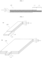
- the first protrudent part 14 and the second protrudent part 15 are not particularly limited in the dimensions and shapes thereof.
- the adhesive sheet 10 may be a tape-shaped adhesive sheet 10 having a configuration that includes a first protrudent part 14 and a second protrudent part 15 which are disposed in an end portion of the adhesive sheet 10, as shown in Fig. 2(a) , or may be a sheet-shaped adhesive sheet 10 having a configuration that includes a first protrudent part 14 and a second protrudent part 15 which project, as shown in Fig. 2(b) .
- Examples of the separator include bases having a releasing layer, lowly bondable bases constituted of a fluoropolymer, and lowly bondable bases constituted of a nonpolar polymer.
- the surface of the separator may have undergone a release treatment, antifouling treatment, or antistatic treatment.
- the thickness of the separator is, for example, 5-200 ⁇ m.
- the adhesive surfaces of the adhesive sheet 10 that is, the surface on the first adhesive layer 11 side and the surface on the second adhesive layer 13 side, have a 180° peel adhesive force (application to SUS304 plate; pulling speed, 300 mm/min; peeling temperature, 23°C) of 0.1 N/10 mm or higher, from the standpoint of attaining satisfactory adhesive force.
- the 180° peel adhesive force of the adhesive sheet 10 can be measured, for example, in the following manner in accordance with JIS Z 0237.
- the adhesive sheet 10 is produced, for example, in the following manner. First, an adhesive composition (first composition) for forming a first adhesive layer 11 and an adhesive composition (second composition) for forming a second adhesive layer 13 are produced. Next, the first composition is applied to the surface of the electroconductive layer 12a of a substrate for voltage application 12 and dried, thereby forming a first adhesive layer 11. Next, the second composition is applied to the surface of the base layer 12b of the substrate for voltage application 12 and dried, thereby forming a second adhesive layer 13.
- the adhesive sheet 10 can be produced, for example, in this manner.
- the joined body 40 according to this embodiment is a joined body including the adhesive sheet 10 according to this embodiment, a first adherend 20, and a second adherend 30, wherein the first protrudent part 14 of the adhesive sheet 10 is folded back toward the second adhesive layer 13, the first adherend 20 is adhered to the electrical debonding type adhesive sheet 10 by a portion of the first adhesive layer 11 which is not folded back, and the second adherend 30 is adhered to the electrical debonding type adhesive sheet 10 by both the second adhesive layer 13 and the folded portion of the first adhesive layer 11 and is in contact with the electroconductive layer lying in the second protrudent part 15.
- the method for joining and separating adherends includes: folding back the first protrudent part 14 of the adhesive sheet 10 according to this embodiment toward the second adhesive layer 13; adhering a first adherend to a portion of the first adhesive layer 11 which is not folded back; adhering a second adherend 30 to both the second adhesive layer 13 and the folded portion of the first adhesive layer 11, thereby joining the first adherend 20 and the second adherend 30 to each other; and thereafter applying a voltage to the first adhesive layer 11 so as to result in a difference in potential in a thickness direction thereof, thereby separating the first adherend 20 and the second adherend 30 from each other.
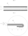
- the second adherend 30 is made to be in stable electrical contact with the electroconductive layer 12a of the adhesive sheet 10 in region B shown in Fig. 4 (or region B' shown in Fig. 5 ). Furthermore, since the second adherend 30 is adhered to the adhesive sheet 10 by both the second adhesive layer 13 and that portion of the first adhesive layer 11 which lies in the folded first protrudent part 14, in regions A and C shown in Fig. 4 (or regions A' and C' shown in Fig. 5 ), stable adhesion can be ensured. There is hence no possibility that the electroconductive layer 12a of the substrate for voltage application 12 might come into contact with an unintended portion to make it impossible to properly apply a voltage to the first adhesive layer 11.
- the first protrudent part 14 is configured of some of the first adhesive layer 11 and some of the substrate for voltage application 12, that is, since the second adhesive layer 13 does not lie in the first protrudent part 14, the increase in thickness due to the folding is minimum. It is hence possible to attain stable joining and to ensure a stable electrical connection between the second adherend 30 and the electroconductive layer 12a.
- the first adherend 20 and the second adherend 30 have electrical conductivity.
- materials constituting such adherends include aluminum, copper, iron, silver, and alloys containing these.
- the materials may be electroconductive polymers, etc. Electrical conductivity is required of at least portions necessary for producing the effects of the present invention. It is only required in the first adherend 20 that at least the portion which is in contact with the first adhesive layer 11 and a portion with which a terminal of a voltage application device is to be contacted have electrical conductivity and these portions are electrically connected. In the second adherend, it is only required that at least the portion which is in contact with the electroconductive layer 12a of the substrate for voltage application 12 and a portion with which the other terminal of the voltage application device is to be contacted have electrical conductivity and these portions are electrically connected.
- the electroconductive layer 12a of the adhesive sheet 10 is in electrical contact with the second adherend 30 and, hence, a voltage can be stably applied by contacting the terminals of a voltage application device with the first adherend 20 and the second adherend 30.
- the voltage to be applied to the first adhesive layer 11 is preferably 1 V or higher, more preferably 3 V or higher, still more preferably 6 V or higher. Meanwhile, the applied voltage is preferably 100 V or less, more preferably 50 V or less, still more preferably 30 V or less, especially preferably 15 V or less. Applied voltages within such a range are suitable because the operation of separating the joined body can be efficiently performed. For example, in cases when the applied voltage is within such a range, an easily available power source such as a dry battery can be used for the voltage application device.
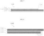
- Fig. 7 is a diagrammatic view of an electrical debonding type adhesive sheet 110 according to the second embodiment of the present invention (hereinafter also referred to simply as “adhesive sheet according to this embodiment” or “adhesive sheet 110").
- the adhesive sheet 110 according to this embodiment is an electrical debonding type adhesive sheet 110 including a substrate for voltage application 112, which includes an electroconductive layer 112a and a base layer 112b, a first adhesive layer 111, which is constituted of an electrically debondable adhesive and is formed on the electroconductive layer 112a of the substrate for voltage application 112, and a second adhesive layer 113, which is formed on the base layer 112b of the substrate for voltage application 112, the electrical debonding type adhesive sheet 110 having a protrudent part 114 in which the second adhesive layer 113 and the substrate for voltage application 112 extend and protrude with respect to the first adhesive layer 111 in a plane direction of the electrical debonding type adhesive sheet 110.
- the layers constituting the adhesive sheet according to the second embodiment are the same as in the adhesive sheet according to the first embodiment, and the only difference is the configuration of the protrudent part.
- the following explanation is given only on points in which the adhesive sheet according to this embodiment differs from the adhesive sheet according to the first embodiment.
- Fig. 8 is exploded diagrammatic view of a joined body 140 according to the second embodiment of the present invention (hereinafter also referred to simply as “joined body 140 according to this embodiment” or “joined body 140").
- Fig. 9 is an enlarged view of the dotted-line-encircled portion of Fig. 8 .
- the joined body 140 according to this embodiment is a joined body including the adhesive sheet 110 according to this embodiment, a first adherend 120, and a second adherend 130, wherein the second adherend 130 is adhered to the electrical debonding type adhesive sheet by the second adhesive layer 130, some of the adhesive sheet 110 is folded back along an end of the second adherend 130 so that some of the second adherend 130 is sandwiched, at least some of the protrudent part 114 is adhered, by the second adhesive layer 113, to that surface of the second adherend 130 which is on the reverse side from the first adherend 120, and the first adherend 120 is adhered to the adhesive sheet 110 by a portion of the first adhesive layer 111 which is not folded back.
- the first adherend 120 has electrical conductivity like the first adherend 20 in the first embodiment. Meanwhile, the second adherend 130 in this embodiment may or may not have electrical conductivity.
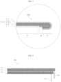
- Fig. 11 is shown a diagrammatic view of the joined body 140 according to this embodiment in which the first adherend 120 and the second adherend 130 are being debonded.
- the first adherend 120 and the second adherend 130 are debonded while applying a voltage to the first adhesive layer 111 via the first adherend 120 and the electroconductive layer 112a of the adhesive sheet 110.
- the terminals of a voltage application device are contacted from the same direction, as shown in Fig. 11 .
- the terminals of a voltage application device are contacted, from the same direction, with the first adherend 120 and the second adherend 130, as shown in Fig. 11 .
Landscapes
- Chemical & Material Sciences (AREA)
- Organic Chemistry (AREA)
- Adhesives Or Adhesive Processes (AREA)
- Adhesive Tapes (AREA)
- Laminated Bodies (AREA)
Priority Applications (1)
| Application Number | Priority Date | Filing Date | Title |
|---|---|---|---|
| EP25175676.3A EP4574425A3 (en) | 2018-03-08 | 2019-03-06 | Electrical debonding type adhesive sheet, joined body, and joining and separation method for adherend |
Applications Claiming Priority (2)
| Application Number | Priority Date | Filing Date | Title |
|---|---|---|---|
| JP2018042353A JP7063660B2 (ja) | 2018-03-08 | 2018-03-08 | 電気剥離型粘着シート、接合体、並びに被着体の接合及び分離方法 |
| PCT/JP2019/008825 WO2019172304A1 (ja) | 2018-03-08 | 2019-03-06 | 電気剥離型粘着シート、接合体、並びに被着体の接合及び分離方法 |
Related Child Applications (2)
| Application Number | Title | Priority Date | Filing Date |
|---|---|---|---|
| EP25175676.3A Division EP4574425A3 (en) | 2018-03-08 | 2019-03-06 | Electrical debonding type adhesive sheet, joined body, and joining and separation method for adherend |
| EP25175676.3A Division-Into EP4574425A3 (en) | 2018-03-08 | 2019-03-06 | Electrical debonding type adhesive sheet, joined body, and joining and separation method for adherend |
Publications (3)
| Publication Number | Publication Date |
|---|---|
| EP3763796A1 EP3763796A1 (en) | 2021-01-13 |
| EP3763796A4 EP3763796A4 (en) | 2021-12-15 |
| EP3763796B1 true EP3763796B1 (en) | 2025-07-09 |
Family
ID=67845727
Family Applications (2)
| Application Number | Title | Priority Date | Filing Date |
|---|---|---|---|
| EP19764294.5A Active EP3763796B1 (en) | 2018-03-08 | 2019-03-06 | Electrical debonding type adhesive sheet, joined body, and joining and separation method for adherend |
| EP25175676.3A Pending EP4574425A3 (en) | 2018-03-08 | 2019-03-06 | Electrical debonding type adhesive sheet, joined body, and joining and separation method for adherend |
Family Applications After (1)
| Application Number | Title | Priority Date | Filing Date |
|---|---|---|---|
| EP25175676.3A Pending EP4574425A3 (en) | 2018-03-08 | 2019-03-06 | Electrical debonding type adhesive sheet, joined body, and joining and separation method for adherend |
Country Status (7)
| Country | Link |
|---|---|
| US (3) | US11623429B2 (enExample) |
| EP (2) | EP3763796B1 (enExample) |
| JP (1) | JP7063660B2 (enExample) |
| KR (1) | KR20200130264A (enExample) |
| CN (1) | CN111819257B (enExample) |
| TW (1) | TW201938726A (enExample) |
| WO (1) | WO2019172304A1 (enExample) |
Families Citing this family (7)
| Publication number | Priority date | Publication date | Assignee | Title |
|---|---|---|---|---|
| KR20230004524A (ko) * | 2020-04-24 | 2023-01-06 | 헨켈 아게 운트 코. 카게아아 | 열 분리형 2 층 점착제 시스템 및 이를 이용한 점착제 디본딩 방법 |
| CN115667447B (zh) | 2021-03-26 | 2023-10-31 | 琳得科株式会社 | 电剥离性粘合片及电剥离性粘合片的剥离方法 |
| EP4194199B1 (en) * | 2021-03-26 | 2025-02-26 | Lintec Corporation | Electrically debondable adhesive sheet, and method for releasing electrically debondable adhesive sheet |
| WO2023282311A1 (ja) * | 2021-07-09 | 2023-01-12 | Dic株式会社 | 粘着テープ、物品、及び物品の解体方法 |
| CN117580920A (zh) * | 2021-07-09 | 2024-02-20 | Dic株式会社 | 粘合带、物品及物品的拆卸方法 |
| JP7685398B2 (ja) * | 2021-08-31 | 2025-05-29 | リンテック株式会社 | 電気剥離性粘着シート |
| CN114261105B (zh) * | 2021-11-23 | 2023-10-03 | 航天海鹰(镇江)特种材料有限公司 | 一种判断钛合金与复材大曲率零件胶接质量的方法 |
Family Cites Families (10)
| Publication number | Priority date | Publication date | Assignee | Title |
|---|---|---|---|---|
| US20080196828A1 (en) | 1999-07-14 | 2008-08-21 | Gilbert Michael D | Electrically Disbonding Adhesive Compositions and Related Methods |
| US7332218B1 (en) | 1999-07-14 | 2008-02-19 | Eic Laboratories, Inc. | Electrically disbonding materials |
| JP2003012903A (ja) | 2001-04-26 | 2003-01-15 | Mitsubishi Rayon Co Ltd | 熱可塑性ポリエステル系樹脂組成物及び該組成物製光反射体 |
| US20090035580A1 (en) | 2005-08-09 | 2009-02-05 | The Yokohama Rubber Co., Ltd. | Electropeeling composition, and making use of the same, adhesive and electropeeling multilayer adhesive |
| JP5733049B2 (ja) * | 2011-06-23 | 2015-06-10 | 日立化成株式会社 | 接着シート、接着シートの製造方法、接着シートロール、半導体装置の製造方法、及び半導体装置 |
| CN105102568B (zh) | 2013-03-27 | 2017-12-29 | 琳得科株式会社 | 电剥离性粘合剂组合物、电剥离性粘合片、以及电剥离性粘合片的使用方法 |
| CN105143385B (zh) | 2013-09-27 | 2017-09-29 | 琳得科株式会社 | 电剥离性粘合剂组合物、电剥离性粘合片、以及电剥离性粘合片的使用方法 |
| JP6974170B2 (ja) | 2015-10-16 | 2021-12-01 | 日東電工株式会社 | 電気剥離用粘着剤組成物、粘着シート、及び接合体 |
| KR102612642B1 (ko) | 2015-10-16 | 2023-12-11 | 닛토덴코 가부시키가이샤 | 양면 점착 시트, 양면 점착 시트 접합체, 및 피착체의 접합·분리 방법 |
| JP6606038B2 (ja) | 2016-09-06 | 2019-11-13 | 株式会社東芝 | 出力電圧制御回路 |
-
2018
- 2018-03-08 JP JP2018042353A patent/JP7063660B2/ja active Active
-
2019
- 2019-03-06 EP EP19764294.5A patent/EP3763796B1/en active Active
- 2019-03-06 US US16/979,014 patent/US11623429B2/en active Active
- 2019-03-06 KR KR1020207024822A patent/KR20200130264A/ko not_active Withdrawn
- 2019-03-06 WO PCT/JP2019/008825 patent/WO2019172304A1/ja not_active Ceased
- 2019-03-06 CN CN201980016859.2A patent/CN111819257B/zh active Active
- 2019-03-06 EP EP25175676.3A patent/EP4574425A3/en active Pending
- 2019-03-08 TW TW108107818A patent/TW201938726A/zh unknown
-
2023
- 2023-03-06 US US18/178,670 patent/US11964462B2/en active Active
-
2024
- 2024-03-20 US US18/610,364 patent/US12441083B2/en active Active
Also Published As
| Publication number | Publication date |
|---|---|
| US12441083B2 (en) | 2025-10-14 |
| US20240217208A1 (en) | 2024-07-04 |
| WO2019172304A1 (ja) | 2019-09-12 |
| JP2019156914A (ja) | 2019-09-19 |
| CN111819257B (zh) | 2023-01-06 |
| EP4574425A3 (en) | 2025-09-24 |
| CN111819257A (zh) | 2020-10-23 |
| US20230256710A1 (en) | 2023-08-17 |
| US20200406582A1 (en) | 2020-12-31 |
| EP4574425A2 (en) | 2025-06-25 |
| EP3763796A1 (en) | 2021-01-13 |
| US11964462B2 (en) | 2024-04-23 |
| JP7063660B2 (ja) | 2022-05-09 |
| TW201938726A (zh) | 2019-10-01 |
| US11623429B2 (en) | 2023-04-11 |
| EP3763796A4 (en) | 2021-12-15 |
| KR20200130264A (ko) | 2020-11-18 |
Similar Documents
| Publication | Publication Date | Title |
|---|---|---|
| US12441083B2 (en) | Electrical debonding adhesive sheet, joined body, and joining and separation method for adherend | |
| US12037522B2 (en) | Electrical debonding type adhesive sheet, joined body, and debonding method for joined body | |
| US11236256B2 (en) | Double-sided adhesive sheet, joined body comprising double-sided adhesive sheet, and method for joining/separating adherends | |
| JP7744122B2 (ja) | 電気剥離型粘着シート、接合体、および接合体の分離方法 | |
| JP2017075289A (ja) | 粘着シート接合体分離方法 |
Legal Events
| Date | Code | Title | Description |
|---|---|---|---|
| STAA | Information on the status of an ep patent application or granted ep patent |
Free format text: STATUS: THE INTERNATIONAL PUBLICATION HAS BEEN MADE |
|
| PUAI | Public reference made under article 153(3) epc to a published international application that has entered the european phase |
Free format text: ORIGINAL CODE: 0009012 |
|
| STAA | Information on the status of an ep patent application or granted ep patent |
Free format text: STATUS: REQUEST FOR EXAMINATION WAS MADE |
|
| 17P | Request for examination filed |
Effective date: 20200907 |
|
| AK | Designated contracting states |
Kind code of ref document: A1 Designated state(s): AL AT BE BG CH CY CZ DE DK EE ES FI FR GB GR HR HU IE IS IT LI LT LU LV MC MK MT NL NO PL PT RO RS SE SI SK SM TR |
|
| AX | Request for extension of the european patent |
Extension state: BA ME |
|
| DAV | Request for validation of the european patent (deleted) | ||
| DAX | Request for extension of the european patent (deleted) | ||
| A4 | Supplementary search report drawn up and despatched |
Effective date: 20211116 |
|
| RIC1 | Information provided on ipc code assigned before grant |
Ipc: C09J 201/00 20060101ALI20211110BHEP Ipc: C09J 7/22 20180101ALI20211110BHEP Ipc: C09J 5/00 20060101ALI20211110BHEP Ipc: B32B 27/00 20060101ALI20211110BHEP Ipc: C09J 7/38 20180101AFI20211110BHEP |
|
| REG | Reference to a national code |
Ref country code: DE Ipc: C09J0007290000 Ref country code: DE Ref legal event code: R079 Ref document number: 602019072307 Country of ref document: DE Free format text: PREVIOUS MAIN CLASS: C09J0007380000 Ipc: C09J0007290000 |
|
| GRAP | Despatch of communication of intention to grant a patent |
Free format text: ORIGINAL CODE: EPIDOSNIGR1 |
|
| STAA | Information on the status of an ep patent application or granted ep patent |
Free format text: STATUS: GRANT OF PATENT IS INTENDED |
|
| RIC1 | Information provided on ipc code assigned before grant |
Ipc: B32B 29/02 20060101ALI20250110BHEP Ipc: B32B 27/36 20060101ALI20250110BHEP Ipc: B32B 27/12 20060101ALI20250110BHEP Ipc: B32B 27/10 20060101ALI20250110BHEP Ipc: B32B 7/12 20060101ALI20250110BHEP Ipc: B32B 7/06 20190101ALI20250110BHEP Ipc: C09J 9/00 20060101ALI20250110BHEP Ipc: C09J 5/00 20060101ALI20250110BHEP Ipc: C09J 7/30 20180101ALI20250110BHEP Ipc: C09J 7/29 20180101AFI20250110BHEP |
|
| INTG | Intention to grant announced |
Effective date: 20250211 |
|
| GRAS | Grant fee paid |
Free format text: ORIGINAL CODE: EPIDOSNIGR3 |
|
| GRAA | (expected) grant |
Free format text: ORIGINAL CODE: 0009210 |
|
| STAA | Information on the status of an ep patent application or granted ep patent |
Free format text: STATUS: THE PATENT HAS BEEN GRANTED |
|
| P01 | Opt-out of the competence of the unified patent court (upc) registered |
Free format text: CASE NUMBER: APP_23162/2025 Effective date: 20250515 |
|
| AK | Designated contracting states |
Kind code of ref document: B1 Designated state(s): AL AT BE BG CH CY CZ DE DK EE ES FI FR GB GR HR HU IE IS IT LI LT LU LV MC MK MT NL NO PL PT RO RS SE SI SK SM TR |
|
| REG | Reference to a national code |
Ref country code: GB Ref legal event code: FG4D |
|
| REG | Reference to a national code |
Ref country code: CH Ref legal event code: EP |
|
| REG | Reference to a national code |
Ref country code: IE Ref legal event code: FG4D |
|
| REG | Reference to a national code |
Ref country code: DE Ref legal event code: R096 Ref document number: 602019072307 Country of ref document: DE |
|
| REG | Reference to a national code |
Ref country code: NL Ref legal event code: MP Effective date: 20250709 |
|
| PG25 | Lapsed in a contracting state [announced via postgrant information from national office to epo] |
Ref country code: PT Free format text: LAPSE BECAUSE OF FAILURE TO SUBMIT A TRANSLATION OF THE DESCRIPTION OR TO PAY THE FEE WITHIN THE PRESCRIBED TIME-LIMIT Effective date: 20251110 |
|
| PG25 | Lapsed in a contracting state [announced via postgrant information from national office to epo] |
Ref country code: NL Free format text: LAPSE BECAUSE OF FAILURE TO SUBMIT A TRANSLATION OF THE DESCRIPTION OR TO PAY THE FEE WITHIN THE PRESCRIBED TIME-LIMIT Effective date: 20250709 |
|
| REG | Reference to a national code |
Ref country code: AT Ref legal event code: MK05 Ref document number: 1811839 Country of ref document: AT Kind code of ref document: T Effective date: 20250709 |