EP3759742B1 - Multi-spectral light sensor - Google Patents
Multi-spectral light sensor Download PDFInfo
- Publication number
- EP3759742B1 EP3759742B1 EP19775519.2A EP19775519A EP3759742B1 EP 3759742 B1 EP3759742 B1 EP 3759742B1 EP 19775519 A EP19775519 A EP 19775519A EP 3759742 B1 EP3759742 B1 EP 3759742B1
- Authority
- EP
- European Patent Office
- Prior art keywords
- light
- layer
- array
- photodiodes
- filter
- Prior art date
- Legal status (The legal status is an assumption and is not a legal conclusion. Google has not performed a legal analysis and makes no representation as to the accuracy of the status listed.)
- Active
Links
Images


Classifications
-
- H—ELECTRICITY
- H10—SEMICONDUCTOR DEVICES; ELECTRIC SOLID-STATE DEVICES NOT OTHERWISE PROVIDED FOR
- H10F—INORGANIC SEMICONDUCTOR DEVICES SENSITIVE TO INFRARED RADIATION, LIGHT, ELECTROMAGNETIC RADIATION OF SHORTER WAVELENGTH OR CORPUSCULAR RADIATION
- H10F77/00—Constructional details of devices covered by this subclass
- H10F77/30—Coatings
- H10F77/306—Coatings for devices having potential barriers
- H10F77/331—Coatings for devices having potential barriers for filtering or shielding light, e.g. multicolour filters for photodetectors
- H10F77/337—Coatings for devices having potential barriers for filtering or shielding light, e.g. multicolour filters for photodetectors using interference filters, e.g. multilayer dielectric filters
-
- G—PHYSICS
- G01—MEASURING; TESTING
- G01J—MEASUREMENT OF INTENSITY, VELOCITY, SPECTRAL CONTENT, POLARISATION, PHASE OR PULSE CHARACTERISTICS OF INFRARED, VISIBLE OR ULTRAVIOLET LIGHT; COLORIMETRY; RADIATION PYROMETRY
- G01J3/00—Spectrometry; Spectrophotometry; Monochromators; Measuring colours
- G01J3/02—Details
- G01J3/0205—Optical elements not provided otherwise, e.g. optical manifolds, diffusers, windows
- G01J3/0229—Optical elements not provided otherwise, e.g. optical manifolds, diffusers, windows using masks, aperture plates, spatial light modulators or spatial filters, e.g. reflective filters
-
- G—PHYSICS
- G01—MEASURING; TESTING
- G01J—MEASUREMENT OF INTENSITY, VELOCITY, SPECTRAL CONTENT, POLARISATION, PHASE OR PULSE CHARACTERISTICS OF INFRARED, VISIBLE OR ULTRAVIOLET LIGHT; COLORIMETRY; RADIATION PYROMETRY
- G01J3/00—Spectrometry; Spectrophotometry; Monochromators; Measuring colours
- G01J3/02—Details
- G01J3/0256—Compact construction
- G01J3/0259—Monolithic
-
- G—PHYSICS
- G01—MEASURING; TESTING
- G01J—MEASUREMENT OF INTENSITY, VELOCITY, SPECTRAL CONTENT, POLARISATION, PHASE OR PULSE CHARACTERISTICS OF INFRARED, VISIBLE OR ULTRAVIOLET LIGHT; COLORIMETRY; RADIATION PYROMETRY
- G01J3/00—Spectrometry; Spectrophotometry; Monochromators; Measuring colours
- G01J3/02—Details
- G01J3/0262—Constructional arrangements for removing stray light
-
- G—PHYSICS
- G01—MEASURING; TESTING
- G01J—MEASUREMENT OF INTENSITY, VELOCITY, SPECTRAL CONTENT, POLARISATION, PHASE OR PULSE CHARACTERISTICS OF INFRARED, VISIBLE OR ULTRAVIOLET LIGHT; COLORIMETRY; RADIATION PYROMETRY
- G01J3/00—Spectrometry; Spectrophotometry; Monochromators; Measuring colours
- G01J3/12—Generating the spectrum; Monochromators
- G01J3/26—Generating the spectrum; Monochromators using multiple reflection, e.g. Fabry-Perot interferometer, variable interference filters
-
- G—PHYSICS
- G01—MEASURING; TESTING
- G01J—MEASUREMENT OF INTENSITY, VELOCITY, SPECTRAL CONTENT, POLARISATION, PHASE OR PULSE CHARACTERISTICS OF INFRARED, VISIBLE OR ULTRAVIOLET LIGHT; COLORIMETRY; RADIATION PYROMETRY
- G01J3/00—Spectrometry; Spectrophotometry; Monochromators; Measuring colours
- G01J3/28—Investigating the spectrum
- G01J3/2803—Investigating the spectrum using photoelectric array detector
-
- H—ELECTRICITY
- H10—SEMICONDUCTOR DEVICES; ELECTRIC SOLID-STATE DEVICES NOT OTHERWISE PROVIDED FOR
- H10F—INORGANIC SEMICONDUCTOR DEVICES SENSITIVE TO INFRARED RADIATION, LIGHT, ELECTROMAGNETIC RADIATION OF SHORTER WAVELENGTH OR CORPUSCULAR RADIATION
- H10F30/00—Individual radiation-sensitive semiconductor devices in which radiation controls the flow of current through the devices, e.g. photodetectors
- H10F30/20—Individual radiation-sensitive semiconductor devices in which radiation controls the flow of current through the devices, e.g. photodetectors the devices having potential barriers, e.g. phototransistors
- H10F30/21—Individual radiation-sensitive semiconductor devices in which radiation controls the flow of current through the devices, e.g. photodetectors the devices having potential barriers, e.g. phototransistors the devices being sensitive to infrared, visible or ultraviolet radiation
- H10F30/288—Individual radiation-sensitive semiconductor devices in which radiation controls the flow of current through the devices, e.g. photodetectors the devices having potential barriers, e.g. phototransistors the devices being sensitive to infrared, visible or ultraviolet radiation the devices being sensitive to multiple wavelengths, e.g. multi-spectrum radiation detection devices
-
- H—ELECTRICITY
- H10—SEMICONDUCTOR DEVICES; ELECTRIC SOLID-STATE DEVICES NOT OTHERWISE PROVIDED FOR
- H10F—INORGANIC SEMICONDUCTOR DEVICES SENSITIVE TO INFRARED RADIATION, LIGHT, ELECTROMAGNETIC RADIATION OF SHORTER WAVELENGTH OR CORPUSCULAR RADIATION
- H10F39/00—Integrated devices, or assemblies of multiple devices, comprising at least one element covered by group H10F30/00, e.g. radiation detectors comprising photodiode arrays
- H10F39/10—Integrated devices
- H10F39/107—Integrated devices having multiple elements covered by H10F30/00 in a repetitive configuration, e.g. radiation detectors comprising photodiode arrays
-
- H—ELECTRICITY
- H10—SEMICONDUCTOR DEVICES; ELECTRIC SOLID-STATE DEVICES NOT OTHERWISE PROVIDED FOR
- H10F—INORGANIC SEMICONDUCTOR DEVICES SENSITIVE TO INFRARED RADIATION, LIGHT, ELECTROMAGNETIC RADIATION OF SHORTER WAVELENGTH OR CORPUSCULAR RADIATION
- H10F77/00—Constructional details of devices covered by this subclass
- H10F77/30—Coatings
- H10F77/306—Coatings for devices having potential barriers
- H10F77/331—Coatings for devices having potential barriers for filtering or shielding light, e.g. multicolour filters for photodetectors
- H10F77/334—Coatings for devices having potential barriers for filtering or shielding light, e.g. multicolour filters for photodetectors for shielding light, e.g. light blocking layers or cold shields for infrared detectors
-
- G—PHYSICS
- G01—MEASURING; TESTING
- G01J—MEASUREMENT OF INTENSITY, VELOCITY, SPECTRAL CONTENT, POLARISATION, PHASE OR PULSE CHARACTERISTICS OF INFRARED, VISIBLE OR ULTRAVIOLET LIGHT; COLORIMETRY; RADIATION PYROMETRY
- G01J3/00—Spectrometry; Spectrophotometry; Monochromators; Measuring colours
- G01J3/28—Investigating the spectrum
- G01J3/2803—Investigating the spectrum using photoelectric array detector
- G01J2003/2806—Array and filter array
-
- G—PHYSICS
- G01—MEASURING; TESTING
- G01J—MEASUREMENT OF INTENSITY, VELOCITY, SPECTRAL CONTENT, POLARISATION, PHASE OR PULSE CHARACTERISTICS OF INFRARED, VISIBLE OR ULTRAVIOLET LIGHT; COLORIMETRY; RADIATION PYROMETRY
- G01J3/00—Spectrometry; Spectrophotometry; Monochromators; Measuring colours
- G01J3/28—Investigating the spectrum
- G01J3/2823—Imaging spectrometer
- G01J2003/2826—Multispectral imaging, e.g. filter imaging
Definitions
- the present disclosure relates to light sensing devices in general, and more particularly, to a multi-spectral light sensor.
- the document US 2016/049449 A1 is a relevant prior art.
- Measuring color is an important part of assessing the operation of various electronic devices, such as printing devices and display devices. Furthermore, measuring color is an important part of assessing the performance of various light sources, such as light emitting diodes (LEDs), fluorescent lights, halogen lights, infra-red (IR) light sources, and ultra-violet (UV) light sources.
- LEDs light emitting diodes
- IR infra-red
- UV ultra-violet
- an optoelectronic device comprising: a photodiode array including a plurality of first photodiodes, each first photodiode including a respective n+ region and a respective n-well region; a guide array disposed over the photodiode array, the guide array including a plurality of guide members separated from one another by a layer of light-blocking material, the guide members being aligned with the n+ regions of the first photodiodes, such that each guide member is disposed over a different respective n+ region, and the layer of light-blocking material being aligned with the n-well regions of the first photodiodes; and a filter array disposed over the guide array, the filter array including a plurality of bandpass filters, each bandpass filter being aligned with a different one of the plurality of guide members, each bandpass filter having a different transmission band.
- an optoelectronic device comprising: a photodiode array including a plurality of first photodiodes; a guide array disposed over the photodiode array, the guide array including a plurality of guide members separated from one another by a layer of light-blocking material, each guide member being aligned with a different one of the plurality of first photodiodes; and a filter array disposed over the guide array, the filter array including a plurality of bandpass filters, each bandpass filter being aligned with a different one of the plurality of guide members, and each bandpass filter having a different respective transmission band.
- a method for manufacturing an optoelectronic device comprising: forming a first layer of light-transmissive material over a photodiode array, the photodiode array including a plurality of photodiodes, each photodiode having a respective n-well region, forming a plurality of first trenches in the first layer of light-transmissive material; forming a layer of light-blocking material in the plurality of first trenches; forming a first metal layer over the first layer of light-transmissive material and the layer of light-blocking material; forming a second layer of light-transmissive material over the first metal layer; forming a plurality of second trenches in the second layer of light-transmissive material, each of the second trenches having a different depth; forming a respective second metal layer in each of the plurality of second trenches; and filling each of the second trenches with a light-transmissive material after the second trench'
- a detector array for measuring characteristics of light.
- the detector array includes a photodiode array and a filter array disposed over the photodiode array.
- the photodiode array includes a plurality of photodiodes.
- the filter array may include a plurality of bandpass filters. Each bandpass filter is positioned over a different photodiode. Furthermore, each bandpass filter has a different transmission band than the rest, thereby enabling its underlying photodiode to measure the energy of the light in the filter's transmission band.
- an energy measurement can be obtained for an entire spectrum of interest.
- the spectrum of interest may encompass one or more of the visible light band, the IR band, and/or the UV band.
- the optoelectronic device includes the detector array and a signal processor that is configured to process the signals generated by the photodiodes in the detector array.
- the signal processor may include an input/output interface that is configured to serially output the signals by the photodiodes in the photodiode array.
- the signal processor may include a processor that is configured to perform one or more arithmetic and logic operations based on the signals generated by the photodiodes in the photodiode array, and output the result of the operations via the I/O interface.
- the processor may be configured to calculate the color of light that is incident upon the optoelectronic device, and output an indication of the color via the I/O interface.
- the detector array may include various adaptations for reducing cross-talk between photodiodes in the photodiode array.
- the detector array includes a guide array that is disposed between the photodiode array and the filter array.
- the guide array includes a plurality of guide members. Each guide member may be formed of a light-transmissive material. Each guide member may be disposed between a different photodiode/filter pair, such that light that is filtered through the filter in the pair is guided by the guide member to the photodiode in the same pair.
- the guide members in the guide array are separated from one another by a layer of light-blocking material.
- the layer of light-blocking material may be formed in the spaces between the guide members in the guide array, thereby reducing the amount of light that can travel between neighboring guide members.
- the layer of light-blocking material may be formed of at least one of a light reflecting material and a light absorbing material.
- the layer of light-blocking material may include three metal layers that are stacked over each other.
- the photodiode array may be configured to reduce cross-talk between the photodiodes in the photodiode array.
- the photodiodes may be CMOS photodiodes including respective n+/p-epi regions and one or more n-well region(s).
- the n-well region(s) may be diffused/implanted to a depth that is greater than the depth at which photons having a predetermined wavelength can penetrate the photodiode array.
- the predetermined wavelength may include any suitable wavelength, such as a wavelength that is in the ultraviolet (UV) band, a wavelength that is in the IR band, and a wavelength that is in the visible light band.
- the n-well regions may reduce the amount of light from traveling between neighboring p+/n+ regions, thereby reducing the amount of cross-talk between the photodiodes in the photodiode array.
- the light-blocking layer of the guide array may be at least partially aligned with the n-well region(s) of the photodiodes in the photodiode array.
- the light-blocking layer of the guide array may be disposed directly over the n-well regions to create a continuous structure which prevents light from traveling sideways.
- This structure may reduce the amount of cross-talk that occurs between the photodiodes in the photodiode array by ensuring that all (or a significant portion of) light that enters the optoelectronic device through a given filter reaches only (or primarily) a given photodiode that is situated under the given filter, without affecting photodiodes that are situated adjacently to the given photodiode.
- aligning the light-blocking layer of the guide array with the n-well region(s) of the photodiode array can significantly improve the accuracy of the resultant detector array.
- FIG. 1A is a diagram of an example of a detector array 100, according to aspects of the disclosure.
- the detector array 100 may include a section 110a that is configured to detect the spectral characteristics of UV light, a section 110b that is configured to detect the spectral characteristics of visible light, and a section 110c that is configured to detect the spectral characteristics of IR light.
- the detector array 100 includes a photodiode array 110, a guide array 120 disposed over the photodiode array, and a filter array 130 disposed over the guide array 120.
- the detector array 100 may include and an IR cutoff filter 140 and IR pass filter 150 disposed over the filter array 130, as shown.
- the photodiode array 110 may include a plurality of photodiodes 112a-i that are formed over a p-substrate 140.
- the photodiodes 112a-c may be P+/n-well photodiodes and they may be used to detect the power of light emissions in the UV band.
- Each of the photodiodes 112a-c may include a respective p+ region 114 that is surrounded on the sides and bottom by an n-well region 117a, and a p-region 118 that is disposed under the n-well region 117a.
- the photodiodes 112d-i may include n+/P- photodiodes and they may be used to detect the power of light emissions in the IR and visible light bands.
- Each of the photodiodes 112d-i may include a respective n+ region 115 that is surrounded on the sides, but not necessarily the bottom, by an n-well region 117b, and a p-region 119 disposed under the n-well region 117b and the n+ regions 115.
- the n-well regions 117a and 117b have the same composition, but alternative implementations are possible in which the n-well regions 117a-b have different compositions.
- n-well regions 117a and 117b may be referred to collectively, as n-well region 117, when appropriate.
- the respective n-well regions 117b of the photodiodes 112d-i may be referred to collectively as "a n-well region" and they might be part of a continuous n-well layer, as shown further below in FIGS. 9A-B .
- the n-well regions 117b may have a secondary function of providing optical insulation between neighboring n+ regions 115 to prevent cross-talk between the photodiodes 112d-i. More particularly, in some implementations, the n+ regions 115 may have a thickness t 1 and the n-well a regions 117b may have a thickness t 2 that is greater than the thickness t 2 . The thickness t 2 may be greater than the depth at which one or more photons having a predetermined frequency can penetrate the photodiode array 110.
- the predetermined frequency may be a frequency in the UV band, a frequency in the IR band, or a frequency in the visible light band.
- the guide array 120 includes a plurality of guide members 124a-i separated by a light-blocking layer 122. Each of the guide members 124a-i may be aligned with a different one of the photodiodes 112a-i, as shown. Furthermore, each of the guide members 124a-i may be formed of a dielectric light-transmissive material.
- the light-transmissive material may include a SiN or SiO2 material and/or any other suitable type of light-transmissive material.
- the light-blocking layer 122 may be formed of at least one of a light reflecting material and/or a light absorbing material.
- the light-blocking layer 122 may be arranged to prevent (or reduce) cross-talk between the guide members 124a-i by preventing light from travelling from one of the guide members 124a-i to another.
- the light-blocking layer 122 may be formed of three metal layers 122a-c that are stacked over one another, as shown, and separated by layers 122d-e.
- any of the metal layers 122a-c may be formed of the same material as the rest. Additionally or alternatively, in some implementations, any of the metal layers 122a-c may be formed of a different material than the rest.
- the metal layer 122a may be formed of aluminum or aluminum-silicon alloy such as Al-Si-Cu
- the metal layer 122b may be formed of Al-Cu alloy sandwiched between titanium nitride barrier layer
- the metal layer 122c may be formed of copper.
- the layers 122d-e may be formed of the same material or different materials.
- the layer 122d may be formed of tungsten plugs with TiN adhesion layer and the layer 122e may be formed of copper.
- the light-blocking layer 122 may be formed concurrently (and/or simultaneously) with the metallization of CMOS logic that is situated on the same die as the detector array 100 (e.g., see the signal processor 405 in FIG. 4 ).
- the structural composition of the light-blocking layer stack may be mainly determined by the implementation of the CMOS or BiCMOS back end of line (BEOL) technologies used.
- the technologies used may include a 3 metal layer or 4 metal layer BEOL technologies.
- the light-blocking layer 122 has a multi-layer structure, alternative implementations are possible in which the light-blocking layer 122 includes only one layer.
- each of the guide members 124a-i may have a thickness in the range of 4.5um to 5.5um. Additionally or alternatively, in some implementations, the light-blocking layer 122 may have a thickness in the range of 6.5um to 7.7um. Additionally or alternatively, in some implementations, the light-blocking layer 122 may have a greater thickness than any of the guide members 124a-i. For example, in such instances, the guide members 124a-i may have a thickness in the range of 4.5um to 5.5um and the light-blocking layer 122 may have a thickness in the range of 6.5um to 7.7um. Additionally or alternatively, in some implementations, the guide array 120 may have a thickness in the range of 7.5um to 8.5um.
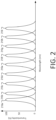
- the filter array 130 includes a plurality of bandpass filters 132a-i. Each of the filters 132a-i may be aligned with a different one of the guide members 124a-i. Furthermore, each bandpass filter has a different transmission band. As illustrated in FIG.
- the filter 132a may have a transmission band 210a (e.g., 300-330 nm); the filter 132b may have a transmission band 210b (e.g., 340-370 nm); the filter 132c may have a transmission band 210c (e.g., 370-400 nm); the filter 132d may have a transmission band 210d (e.g., 400-500 nm); the filter 132e may have a transmission band 210e (e.g., 500-600 nm); the filter 132f may have a transmission band 210f (e.g., 600-700 nm); the filter 132g may have a transmission band 210g (e.g., 700-800 nm); the filter 132h may have a transmission band 210h (e.g., 800-900 nm); and the filter 132i may have a transmission band 210i (e.g., 900-1000 nm).
- the filter 132e may
- the filter array 130 may include a plurality of metal layers 134 and a plurality of metal layers 136. Each of the metal layers 134 may be aligned with a different one of the metal layers 136. Additionally or alternatively, each of the metal layers 134 may be spaced apart by a different distance from the metal layer 136 with which the metal layer 134 is aligned. In some implementations, a metal layer 136 may be considered to be aligned with a given metal layer 134 if at least some of light passing through the metal layer 136 reaches the given metal layer 134. Additionally or alternatively, in some implementations, a metal layer 136 may be considered to be aligned with a given metal layer 134, if at least a portion of the metal layer 136 is situated directly above the given metal layer 134.
- the metal layers 134 and 136 may be suspended in a layer of light-transmissive material 138, as shown.
- the metal layers 134 and 136 may be formed of any suitable type of material.
- any of the metal layers 134 and 136 may be formed of an alloy including aluminum and silver.
- the layer of light-transmissive material may include a SiN material and/or any other suitable type of light-transmissive material like silicon dioxide SiO2.
- each of the metal layers 134 may have a thickness in the range of 400A to 600A. Additionally or alternatively, in some implementations, each of the metal layers 136 may have a thickness in the range of 400A to 600A. Additionally or alternatively, in some implementations, the entire filter array 130 may have a thickness in the range of 0.125um to 0.4um.
- Each of the filters 132a-i in the filter array 130 may include a respective one of the respective metal layer 136 and a different one of the metal layers 134 that is situated underneath the metal layer 136.
- the distance between the metal layers 134 and 136 in any of the filters 132a-i may be different from the distance between the metal layers 134 and 136 in the remaining ones of the filters 132a-i.
- each of the filters 132a-i may include a different Fabry-Perot cavity that is formed by the filter's respective metal layer 136 and the metal layer 134.
- filters 132a-i are implemented using Fabry-Perot cavities
- another type of filter such as double stack of Fabry-Perot cavity having three metal layers and two layer of light-transmissive materials forming a stack including Ag/SIN/Ag/SIN/Ag layers.
- FIG. 1B shows the configuration of the filter 132a in further detail, in accordance with one particular implementations.
- the structure of the filters 132b-i may be the same or similar to that of the filter 132a.
- FIG. 1B is provided to clearly show the spatial relationship between each (or at least one) of the metal layers 134 and the light-blocking layer 122. Shown in FIG. 1B is a portion of the guide member 124a and a portion of the light-blocking layer 122. As illustrated in FIG.
- the light-blocking layer 122 may have a thickness that is greater than the thickness of the guide member 124a, such that a top surface 123 of the light-blocking layer 122 is situated above the top surface 125 of the guide member 124a.
- the metal layer 136 may include a central portion 136a and end portions 136b that are inclined relative to the central portion 136a.
- the metal layer 134 may include a central portion 134a and end portions 134b that are inclined relative to the central portion 134a. In some implementations, the entire central portion 134a of the metal layer 134 may be situated below the level of the top surface 123 of the light-blocking layer 122.
- only some of the central portion 134a of the metal layer 134 may be situated below the level of the top surface 123 of the light-blocking layer.
- situating at least some of the central portion 134a of the metal layer 134 below the level of the top surface 123 of the light-blocking layer 132 may reduce the amount of cross-talk between the filter 132a and neighboring filters to greatly improve the resolution of the filter array 130.
- the level of the top surface 123 is denoted by a dashed line.
- the metal layer 134 includes a horizontal central portion 134a and inclined end-portions 134b, alternative implementations are possible in which the inclined end-portions 134b are omitted.
- the metal layer 136 includes a horizontal central portion 136a and inclined end-portions 136b, alternative implementations are possible in which the inclined end-portions 136b are omitted.
- the metal layer 134 can be regarded as different segments (or portions) of the same discontinuous metal layer. In this regard, it will be understood that alternative implementations are possible in which the metal layers 134 are replaced by a single continuous metal layer (e.g., see the metal layer 1510 which is shown in FIGS. 15A-B ).
- the metal layers 136 can be regarded as different segments (or portions) of the same discontinuous metal layer.
- the metal layers 136 are replaced by a single continuous metal layer (e.g., see the metal layer 1810 which are shown in FIGS. 15A-B ).
- the IR-cutoff filter 140 may be disposed over the filters 132d-f. In some implementations, the IR-cutoff filter 140 may be arranged to block light having a wavelength that is greater than 700 nm and transmit light having a wavelength that is less than 700 nm. Additionally or alternatively, in some implementations, the IR-cutoff filter 140 may have a thickness in the range of 4um to 5 um.
- the IR-pass filter 150 may be disposed over the filters 132g-i. In some implementations, the IR-pass filter may be arranged to block light having a wavelength that is less than 700 nm and transmit light having a wavelength that is greater than 700nm.
- the IR-pass filter 150 may have a thickness in the range of 2um to 2.5um. Any of the IR-cutoff filter 140 and the IR-pass filter 150 may be an absorption filter based on organic dye or pigment. Any of the IR-cutoff filter 140 and the IR-pass filter 150 may be may be formed on top of the filter array 130 by using spin coating and/or any other suitable process. Additionally or alternatively, in some implementations, the IR-cutoff filter 150 can be a metallic interference IR-cutoff filter including silver and a dielectric material, such as Nb 2 0 5 (niobium pentoxide), with a total thickness of 1um.
- a dielectric material such as Nb 2 0 5 (niobium pentoxide
- the Ag thickness may be about 100A and the Nb 2 0 5 thickness may be in the range of 500A to 600A.
- the IR-cutoff filter 140 and the IR-pass filter 150 may be replaced with a full dielectric IR-cutoff filter that is configured to block wavelengths lower than 400nm and wavelengths larger than 700nm. The total thickness of such full dielectric IR-cutoff filter may be in the range of 4.5um to 5.5um.
- FIG. 1C is a top-down view of the detector array 100 with the IR-cutoff filter 140 and the IR-pass filter 150 removed.
- FIG. 1C illustrates that the photodiodes 112a-i, the guide members 124a-i, and the filters 132a-i may be aligned to form a plurality of detector cells 160a-i.
- the filter 132a may be aligned with the guide member 124a, and the guide member 124a may be aligned with the photodiode 112a.
- the filter 132a, the guide member 124a, and the photodiode 112a may together form the detector cell 160a.
- the filter 132b may be aligned with the guide member 124b, and the guide member 124b may be aligned with the photodiode 112b. As a result, the filter 132b, the guide member 124b, and the photodiode 112b may together form the detector cell 160b.
- the filter 132i may be aligned with the guide member 124i, and the guide member 124i may be aligned with the photodiode 112i. As a result, the filter 132i, the guide member 124i, and the photodiode 112i may together form the detector cell 160i.
- a guide member may be considered to be aligned with an underlying photodiode if at least some of light passing through the guide member can reach the photodiode. Additionally or alternatively, in some implementations, a guide member may be considered to be aligned with an underlying photodiode if the guide member is disposed directly above the photodiode. Additionally or alternatively, in some implementations, a guide member may be considered to be aligned with an underlying photodiode if the guide member is disposed partially above the photodiode, such that a portion of the guide member is situated directly above the photodiode and another portion is overhanging the photodiode.
- a filter may be considered to be aligned with an underlying guide member if at least some of light passing through the filter can reach the guide member. Additionally or alternatively, in some implementations, a filter may be considered to be aligned with an underlying guide member if the filter is disposed directly above the guide member. Additionally or alternatively, in some implementations, a filter may be considered to be aligned with an underlying guide member if the filter is disposed partially above the guide member, such that a portion of the filter is situated directly above the guide member and another portion is overhanging the guide member.
- the detector cells 160a-i may be optically insulated from one another to eliminate (or reduce) the amount of crosstalk between the cells 160a-i, or the photodiodes 112a-i, in particular.
- the optical insulation may be provided by the light-blocking layer 122 which, as noted above, may prevent (or reduce the amount of) light travelling from one of the guide member 124a-i to another one of the guide member 124a-i.
- the optical insulation may be provided by the n-well region(s) 117 which, as noted above, may be arranged to prevent light that has reached one photodiode from travelling across that photodiode to reach neighboring photodiodes.
- the light-blocking layer 122 may be aligned with the guide layer(s) 124a-i to form a continuous structure that prevents (or reduces the amount of) light that can travel from one of the detector cells 160a-i to another one of the detector cells 160a-i.
- at least a portion of the light-blocking layer 122 may be situated directly above the n-well region(s) 117a and/or the n-well region(s) 117b.
- aligning the light-blocking layer of the guide array with the n-well region(s) of the photodiode array may improve the accuracy of the detector array 100.
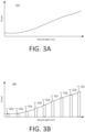
- FIGS. 3A-B illustrate the operation of the detector array 100, according to aspects of the disclosure. Shown in FIG. 3A is a plot 310, which illustrates the spectral content of a test light. Shown in FIG. 3B is a plot 320, which illustrates the response of the detector array 100 to the test light. FIGS. 3A-B illustrate that when the detector array 100 is exposed to the test light, the signals generated by the photodiodes 112a-i in the detector array 100 may be used to reconstitute the spectral content of the test light over a given range of interest.
- the magnitude of each signal that is generated by the photodiodes 112a-i may be represented by a different one of the bars 322a-i. More particularly, the bar 322a may represent the magnitude of a signal (e.g., a voltage signal) generated by the photodiode 112a; the bar 322b may represent the magnitude of a signal generated by the photodiode 112b; and the bar 322c may represent the magnitude of a signal that is generated by the photodiode 112c.
- a signal e.g., a voltage signal
- FIG. 4 is a diagram of an example of an optoelectronic device 400, according to aspects of the disclosure.
- the optoelectronic device 400 includes the detector array 100 and a signal processor 405.
- the detector array 100 and the signal processor 405 may be integrated on the same die or they may be formed on separate dies.
- the signal processor may include any suitable type of processing circuitry.
- the signal processor 405 may include one or more of a switch 410, an amplifier 420, an analog-to-digital converter (ADC) 430, a processor 440, and an input/output (I/O) interface 450.
- ADC analog-to-digital converter
- I/O input/output
- the switch 410 may include any suitable type of electronic device that is configured to receive a plurality of signals from the photodiodes 112a-i and feed the signals, one at a time, to the amplifier 420.
- the amplifier 420 may include any suitable type of device that is configured to increase the power of the signals generated by the photodiodes 112a-i.
- the ADC 430 may include any suitable type of device that is configured to generate a digital representation of an analog signal that is input into the ADC 430.
- the ADC 430 may include a 16-bit ADC, a 32-bit ADC, a 64-bit ADC, etc.
- the processor 440 may include any suitable type of electronic circuitry that is capable of performing one or more arithmetic or logic operations based on values generated by the ADC 430.
- the I/O interface 450 may include any suitable type of parallel or serial interface, such as a Universal Serial Bus (USB) interface or an I 2 C interface, etc.
- USB Universal Serial Bus
- the photodiodes 112a-b may generate a plurality of signals representing the power of different portions of the spectrum of light that is incident on the detector array 100.
- the switch 410 may switch the signals, such that each of the signals generated by the photodiodes 112a-i is supplied to the amplifier 420.
- the amplifier 420 may amplify each of the signals and feed it to the ADC 430.
- the ADC 430 may produce a digital representation of each of the signals and supply the digital representation to the processor 440.
- the processor 440 may detect a characteristic of light, such as correlated color temperature (CCT) or color.
- CCT correlated color temperature
- the optoelectronic device includes the processor 440
- the processor 440 is omitted.
- the digital representations of the signals generated by the photodiodes 112a-i may be output from the I/O interface for use by external processing circuitry.
- the amplifier 420 is a 1-channel amplifier
- the switch 410 may be configured to provide multiple signals to the amplifier 420 in parallel.
- the amplifier 420 may be an 8-channel amplifier and the switch 410 may be configured to feed in parallel signals from 8 different detector cells to the amplifier.
- FIG. 5 depicts an example of a mathematical operation, which the processor 440 may be configured to perform, according to aspects of the disclosure.
- the processor 440 may be configured to generate a vector 510 which identifies the color of light applied to the detector array 100 in the CIE 1931 color space.
- the vector 510 may include tristimulus values X, Y, Z which provide an objective description of color sensation registered in the human eye.
- the processor 440 generates a representation of light in the CIE 1394 color space, alternative implementations are possible in which another type of representation is created, such as a representation in the RGB color space or a representation in the YCrCb color space.
- the vector 510 may be calculated by multiplying a vector 530 by a coefficient matrix 520.
- the vector 530 may include the values Va-Vi which represent the values of the signals generated by different photodiodes in the detector array 100.
- value Va may represent the magnitude of the signal generated by the photodiode 112a
- value Vb may represent the magnitude of the signal generated by the photodiode 112b
- value Vc may represent the magnitude of the signal generated by the photodiode 112c
- value Vd may represent the magnitude of the signal generated by the photodiode 112d
- value Ve may represent the magnitude of the signal generated by the photodiode 112e
- value Vf may represent the magnitude of the signal generated by the photodiode 112f
- value Vg may represent the magnitude of the signal generated by the photodiode 112g
- value Vh may represent the magnitude of the signal generated by the photodiode 112h
- value Vi may represent the magnitude of the signal generated by the
- the coefficient matrix 520 may be a matrix that is pre-stored in a memory (not shown) of the processor 440.
- the coefficient matrix may be calculated by calibrating the optoelectronic device 400 with a known or standard reference light source. The calibration may be performed by exposing the optoelectronic device 400 to a calibration light whose color is known, and solving the equation shown in FIG. 5 for the coefficient matrix 520.
- FIG. 6 is a schematic diagram of an example of optoelectronic device 600, according to aspects of the disclosure.
- the optoelectronic device includes a detector array 610 and a signal processor 620.
- the detector array 610 may include detector cells 160a-i, as shown.
- the detector array 610 may be the same or similar to the detector array 100, except for the sensors cells 160a-i being arranged in a grid.
- the signal processor 620 may be the same or similar to the signal processor 405, which is discussed above with respect to FIG. 4 .
- FIG. 7 is a schematic diagram of an example of an optoelectronic device 700, according to aspects for the disclosure.
- the optoelectronic device 700 may be the same or similar to the optoelectronic device 600, but for including an IR-cutoff filter 740 and an IR-pass filter 750, as shown.
- the IR-cutoff filter 740 may be disposed over cells 160d, 160e, and 160f of the detector array 610 and it may be the same or similar to the IR-cutoff filter 140.
- the IR-pass filter 750 may be disposed over cells 160g, 160h, and 160i of the detector array 610 and it may be the same or similar to the IR-pass filter 150.
- FIG. 8 is a flowchart of an example of a process 800 for manufacturing a detector array, according to aspects of the disclosure.
- a photodiode array 910 is formed.
- An example of the photodiode array 910 is shown in FIGS. 9A-C .
- the photodiode array may include photodiodes 912a-i formed on a p-substrate 940.
- the photodiodes 912a-c may be the same or similarto the photodiodes 112a-c, which are discussed above with respect to FIGS. 1A-B .
- the photodiodes 912d-i may be the same or similar to the photodiodes 112d-i, which are discussed above with respect to FIG. 1 .
- the photodiodes 912a-c may be p+/n-well diodes and they may be used to detect the power of light emissions in the UV band.
- Each of the photodiodes 912a-c may include a respective p+ region 914 that is surrounded on sides and bottom by an n-well region 917a, and a p-region 918 that is disposed under the n-well region 917a.
- the p+ regions 914 may be the same or similar to the p+ regions 114
- the n-well region 917a may be the same or similar to the n-well region 117a
- the p-region 918 may be the same or similar to the p-region 118.
- the photodiodes 912d-i may include n+/P-epi photodiodes and they may be used to detect light in the IR and visible light bands.
- Each of the photodiodes 912d-i may include a respective n+ region 915 that is surrounded on the sides by the n-well region 917b, and a p-region 919 disposed under the n-well region 917b and the n+ regions 915.
- the n+ regions 915 may be the same or similar the n+ regions 115
- the n-well region(s) 917b may be the same or similar as the n-well region 117b
- the p-region 919 may be the same or similar to the p-region 119.
- a layer of dielectric light-transmissive material 1010 is formed over the photodiode array 910.
- An example of the light-transmissive layer 1010 is shown in FIGS. 10A-B .
- the layer of light-transmissive material may be formed of any suitable type of material, such as silicon dioxide including Borophosphosilicate glass (BPSG), phosphosilicate glass (PSG), undoped silica glass (USG) and fluorosilicate glass (FSG) glass materials, etc.
- the layer of light-transmissive material 1010 may be formed using plasma-enhanced chemical vapor deposition (PECVD) and/or any other suitable type of process.
- PECVD plasma-enhanced chemical vapor deposition
- the layer of light-transmissive material 1010 may be separated from the photodiode array 910 by a passivation layer (not shown).
- the passivation layer may be formed of silicon dioxide SiO 2 and Silicon Nitride Si 3 N 4 .
- the layer of light-transmissive 1010 material may have a thickness in the range of 5um - 7.5um.
- a plurality of trenches 1110 are formed into the layer of light-transmissive material 1010 to define a plurality of guide members 1012.
- the guide members 1012 may be the same or similar to the guide members 124a-i.
- An example of the trenches 1110 is shown in FIGS.11A-C .
- the trenches 1110 may be formed above at least a portion of the n-well regions 917b. Additionally or alternatively, in some implementations, the trenches 1110 may be formed above portions of the n-well region 917a that are situated between adjacent p+ regions 914.
- the trenches 1110 may be formed above portions of the n-well region 917b that are situated between adjacent n+ regions 915.
- the trenches 1110 may be formed using CMOS or BICMOS back end of line process and/or any other suitable type of process.
- the trenches 1110 may have a depth that is less than, greater than, or equal to the thickness of the light-transmissive layer 1010.
- a light-blocking layer 1210 is formed in the trenches 1110 to complete a guide array 1120.
- An example of the light-blocking layer 1210 and the guide array 1220 is shown in FIGS.12A-B .
- the guide array 1220 may include the guide members 1012 and the light-blocking layer 1210, as shown.
- the guide array 1220 may be the same or similar to the guide array 120, which is discussed above with respect to FIGS. 1A-B .
- the light-blocking layer 1210 may be the same or similar to the light-blocking layer 122, which is discussed above with respect to FIGS. 1A-C .
- the light-blocking layer 1210 may have thickness in the range of 4.5um to 5.5um for a 3 metal layer process. In some implementations, the light-blocking layer 1210 may have a greater thickness than the layer of light-transmissive material 1010, such that the top surface of the light-blocking layer 1210 is situated above the top surface of the layer of light-transmissive material 1310.
- a layer of dielectric light-transmissive material 1310 is formed over the photodiode array.
- An example of the layer of light-transmissive material 1310 is shown in FIGS.13A-B .
- the layer of light-transmissive material 1310 may be formed using any suitable type of material, such as a Si 3 N 4 material, Al 2 O 3 , HfO 2 , SiO 2 , TiO 2 , Nb 2 O 5 .
- LPCVD low pressure chemical vapor deposition
- ALD atomic layer deposition
- a plurality of trenches 1410 is formed into the layer of light-transmissive material 1310.
- An example of the trenches 1410 is shown in FIGS. 14A-B .
- the trenches 1410 may have substantially the same depth and each of the trenches 1410 may be formed above a different one of the photodiodes 912a-i.
- each of the trenches 1410 may extend below the level of the top surface of the light-blocking layer 1210, as shown.
- the level of the top surface of the light-blocking layer 1210 is denoted by a dashed line in FIGS. 14A-B .
- the trenches 1410 may be formed using low temperature plasma etching or atomic layer precision etching (ALE) systems and/or any other suitable type of process.
- ALE atomic layer precision etching
- a metal layer 1510 is formed over the layer of light-transmissive material 1310.
- An example of the metal layer 1510 is shown in FIGS. 15A-B .
- the metal layer 1510 may be formed of any suitable material, such as silver, aluminum, gold or copper etc.
- the metal layer may be formed using an alloy including aluminum (Al) and silver (Ag).
- the metal layer 1510 may be formed using any suitable type of process, such as thermal evaporation, electron gun deposition with ion assist deposition, and sputter deposition for example.
- portions of the metal layer 1510 that are formed on the bottom of the trenches 1410 may be at least partially situated below the level of the top surface of the light-blocking layer 1210.
- the level of the top surface of the light-blocking layer 1210 is denoted by a dashed line in FIGS. 15A-B .
- a layer of dielectric light-transmissive material 1610 is formed over the metal layer 1510.
- An example, of the layer of light-transmissive material 1610 is shown in FIGS. 16A-B .
- the layer of light-transmissive material 1610 may be formed using any suitable type of material, such as a Si3N4 material, Al 2 O 3 , HfO 2 , SiO 2 , TiO 2 , Nb 2 O 5 .
- low pressure chemical vapor deposition (LPCVD) and atomic layer deposition (ALD) may be used to form the layer 1610.
- the layer of light-transmissive material 1610 may have a thickness in the range of 1200A to 2500A.
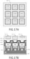
- a plurality of trenches 1710 is formed into the layer of light-transmissive material 1610.
- An example of the trenches 1710 is shown in FIGS. 17A-B .
- at least one of the trenches 1710 may have a different depth than at least one other trench 1710.
- each of the trenches 1710 may have a different depth than the rest.
- each of the trenches 1710 may be formed over a different one of the photodiodes 912a-i in the photodiode array 910, as shown.
- the trenches 1710 may be formed using low temperature plasma etching or atomic layer precision etching (ALE) systems and/or any other suitable type of process.
- ALE atomic layer precision etching
- a metal layer 1810 is formed over the light-transmissive layer 1610 and the trenches 1710, as shown.
- An example of the metal layer 1810 is shown in FIGS. 18A-B .
- the metal layer 1810 may be formed of an alloy including aluminum (Al) and silver (Ag).
- the metal layer 1810 may be formed using silver, aluminum, gold, copper and/or any other suitable type of material.
- the metal layer 1510 may be formed using any suitable type of process, such as thermal evaporation, electron gun deposition with ion assist deposition, and sputter deposition for example.
- the layer 1810 may have a thickness in the range of 400A to 600A depending on the bandwidth requirement of the band pass filter design.
- a layer of light-transmissive material 1905 is formed over the metal layer 1810 to complete a filter array 1910.
- An example of the filter array 1910 is shown in FIGS. 19A-B .
- the layer of light-transmissive material 1905 may be formed using any suitable type of material, such as a SisN 4 material, Al 2 O 3 , HfO 2 , SiO 2 , TiO 2 , Nb 2 O 5 .
- low pressure chemical vapor deposition (LPCVD) and atomic layer deposition (ALD) may be used to form the layer 1905.
- LPCVD low pressure chemical vapor deposition
- ALD atomic layer deposition
- the filter array 1910 may be the same or similar to the filter array 130, which is discussed above with respect to FIGS. 1A-B .
- FIGS. 19A-B show an example of a resultant detector array 1920 that is produced as a result of performing steps 805-855 of the process 800.
- the detector array 1920 may include plurality of detector cells 160a-i.
- the detector cells in the detector array 1920 may be similar to the detector cells in the detector array 100 and the detector cells in the detector array 610, which are discussed above with respect to FIGS. 1A-B and 6 .
- the detector cells 160a-c may be arranged to measure the energy of light emissions in the UV band
- the cells 160d-f may be arranged to measure the energy of light emissions in the visible light band
- the cells 160g-i may be arranged to measure the energy of light in the IR band.
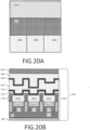
- an IR-cutoff filter 2010 is formed over the detector cells 160d-f of the detector array 1720 and an IR-pass filter 2020 is formed over the detector cells 160g-i of the detector array 1920 to complete an optoelectronic device 2030.
- the IR-cutoff filter 2010 may be the same or similar to the IR-cutoff filter 140. Additionally or alternatively, in some implementations, the IR-cutoff filter 2010 may be the same or similar to the IR-pass filter 150.
- An example of the filters 2010 and 2020 is shown in FIGS. 20A-B .
- FIGS. 1-20B are provided as an example only. At least some of the elements discussed with respect to these figures can be arranged in different order, combined, and/or altogether omitted. It will be understood that the provision of the examples described herein, as well as clauses phrased as "such as,” “e.g.”, “including”, “in some aspects,” “in some implementations,” and the like should not be interpreted as limiting the disclosed subject matter to the specific examples.
- the term “light-transmissive material” may refer to any material having a light transmissivity greater than 80% to 95%.
- that the term “light-blocking material” may refer to any material having a light transmissivity less than 2% to 0.1%.
Landscapes
- Physics & Mathematics (AREA)
- Spectroscopy & Molecular Physics (AREA)
- General Physics & Mathematics (AREA)
- Light Receiving Elements (AREA)
- Solid State Image Pick-Up Elements (AREA)
- Spectrometry And Color Measurement (AREA)
- Transforming Light Signals Into Electric Signals (AREA)
- Color Television Image Signal Generators (AREA)
- Photometry And Measurement Of Optical Pulse Characteristics (AREA)
- Engineering & Computer Science (AREA)
- Manufacturing & Machinery (AREA)
Applications Claiming Priority (2)
| Application Number | Priority Date | Filing Date | Title |
|---|---|---|---|
| US15/941,855 US10770489B2 (en) | 2018-03-30 | 2018-03-30 | Optoelectronic device arranged as a multi-spectral light sensor having a photodiode array with aligned light blocking layers and N-well regions |
| PCT/US2019/024761 WO2019191543A1 (en) | 2018-03-30 | 2019-03-29 | Multi-spectral light sensor |
Publications (3)
| Publication Number | Publication Date |
|---|---|
| EP3759742A1 EP3759742A1 (en) | 2021-01-06 |
| EP3759742A4 EP3759742A4 (en) | 2022-03-30 |
| EP3759742B1 true EP3759742B1 (en) | 2024-03-13 |
Family
ID=68053873
Family Applications (1)
| Application Number | Title | Priority Date | Filing Date |
|---|---|---|---|
| EP19775519.2A Active EP3759742B1 (en) | 2018-03-30 | 2019-03-29 | Multi-spectral light sensor |
Country Status (8)
| Country | Link |
|---|---|
| US (2) | US10770489B2 (https=) |
| EP (1) | EP3759742B1 (https=) |
| JP (1) | JP7610982B2 (https=) |
| KR (1) | KR102747259B1 (https=) |
| CN (1) | CN112088434B (https=) |
| IL (1) | IL277562B2 (https=) |
| TW (1) | TWI809074B (https=) |
| WO (1) | WO2019191543A1 (https=) |
Families Citing this family (19)
| Publication number | Priority date | Publication date | Assignee | Title |
|---|---|---|---|---|
| US12009379B2 (en) * | 2017-05-01 | 2024-06-11 | Visera Technologies Company Limited | Image sensor |
| US10770489B2 (en) * | 2018-03-30 | 2020-09-08 | Vishay Intertechnology, Inc. | Optoelectronic device arranged as a multi-spectral light sensor having a photodiode array with aligned light blocking layers and N-well regions |
| US11287368B2 (en) * | 2018-07-13 | 2022-03-29 | Halliburton Energy Services, Inc. | Thin film multivariate optical element and detector combinations, thin film optical detectors, and downhole optical computing systems |
| US10651220B2 (en) | 2018-07-30 | 2020-05-12 | Taiwan Semiconductor Manufacturing Co., Ltd. | Narrow band filter with high transmission |
| DE112019004426T5 (de) * | 2018-09-04 | 2021-06-02 | Ams Ag | Biomarker-Leser |
| US11404468B2 (en) | 2019-06-21 | 2022-08-02 | Taiwan Semiconductor Manufacturing Company, Ltd. | Wavelength tunable narrow band filter |
| CN110931516B (zh) * | 2019-11-18 | 2021-11-19 | 中国科学院上海技术物理研究所 | 一种用于红外宽光谱分光快速测温的碲镉汞光导器件 |
| GB2595305A (en) * | 2020-05-22 | 2021-11-24 | Ams Ag | Optical detector |
| JP7818358B2 (ja) * | 2020-07-23 | 2026-02-20 | 三星電子株式会社 | イメージセンサ及びイメージ処理方法、並びにイメージセンサを含む電子装置 |
| JPWO2022044692A1 (https=) * | 2020-08-24 | 2022-03-03 | ||
| GB202015948D0 (en) * | 2020-10-08 | 2020-11-25 | ams Sensors Germany GmbH | Multi-spectral optical sensor and system |
| CN121712249A (zh) | 2020-10-23 | 2026-03-20 | Tdk株式会社 | 接收装置、发送接收装置、通信系统和便携终端装置 |
| JP2022101452A (ja) * | 2020-12-24 | 2022-07-06 | Tdk株式会社 | 光センサー、光センサーユニット、光センサー装置及び情報端末装置 |
| CN115236782B (zh) * | 2021-04-22 | 2026-03-13 | 三星电子株式会社 | 光谱滤波器以及包括光谱滤波器的图像传感器和电子设备 |
| US20230093853A1 (en) * | 2021-09-30 | 2023-03-30 | Samsung Electronics Co., Ltd. | Spectral filter, and image sensor and electronic device including the spectral filter |
| US20230157061A1 (en) * | 2021-11-17 | 2023-05-18 | The Trustees Of Princeton University | Reconfigurable thin-film photonic filter banks for neuromorphic opto-electronic systems and methods |
| CN114526816B (zh) * | 2021-12-29 | 2024-03-15 | 光沦科技(深圳)有限公司 | 一种微型多光谱-3d多模式相机系统及成像方法 |
| US20240145298A1 (en) * | 2022-10-26 | 2024-05-02 | Taiwan Semiconductor Manufacturing Company, Ltd. | Doping free connection structures and methods |
| TWI828466B (zh) * | 2022-12-08 | 2024-01-01 | 台亞半導體股份有限公司 | 光電二極體結構 |
Family Cites Families (36)
| Publication number | Priority date | Publication date | Assignee | Title |
|---|---|---|---|---|
| JPS6457134A (en) * | 1987-08-27 | 1989-03-03 | Minolta Camera Kk | Spectrum measuring sensor |
| US6665012B1 (en) | 1998-09-22 | 2003-12-16 | Pixim, Inc. | Process-scalable high spatial resolution and low bit resolution CMOS area image sensor |
| KR100464321B1 (ko) * | 2002-11-20 | 2004-12-31 | 삼성전자주식회사 | 실리콘 광소자 및 이를 적용한 화상 입출력장치 |
| KR20040060509A (ko) * | 2002-12-30 | 2004-07-06 | 동부전자 주식회사 | Cmos 이미지 센서 |
| US7521666B2 (en) | 2005-02-17 | 2009-04-21 | Capella Microsystems Inc. | Multi-cavity Fabry-Perot ambient light filter apparatus |
| US8084728B2 (en) * | 2005-07-06 | 2011-12-27 | Capella Microsystems, Corp. | Optical sensing device |
| JP4984706B2 (ja) * | 2006-07-19 | 2012-07-25 | 株式会社デンソー | マイクロ構造体の製造方法 |
| US7626241B1 (en) * | 2007-04-23 | 2009-12-01 | Texas Advanced Optoelectronic Solutions, Inc. | Thin film interference ripple reduction |
| JP5023808B2 (ja) * | 2007-05-24 | 2012-09-12 | ソニー株式会社 | 固体撮像装置およびカメラ |
| US8229255B2 (en) | 2008-09-04 | 2012-07-24 | Zena Technologies, Inc. | Optical waveguides in image sensors |
| WO2010069997A1 (en) | 2008-12-16 | 2010-06-24 | Dyrup A/S | Self-cleaning coating composition |
| JP2010232509A (ja) | 2009-03-27 | 2010-10-14 | Oki Semiconductor Co Ltd | 光半導体および光半導体の製造方法 |
| US9357956B2 (en) * | 2010-03-05 | 2016-06-07 | Seiko Epson Corporation | Spectroscopic sensor and electronic apparatus |
| JP2011199050A (ja) * | 2010-03-19 | 2011-10-06 | Sony Corp | 固体撮像デバイスおよび電子機器 |
| JP2012156310A (ja) * | 2011-01-26 | 2012-08-16 | Sony Corp | 固体撮像素子、固体撮像素子の製造方法、および電子機器 |
| KR20120110377A (ko) * | 2011-03-29 | 2012-10-10 | 삼성전자주식회사 | 이미지 센서 |
| JP5803419B2 (ja) * | 2011-08-19 | 2015-11-04 | セイコーエプソン株式会社 | 傾斜構造体、傾斜構造体の製造方法、及び分光センサー |
| JP6253870B2 (ja) | 2011-10-04 | 2017-12-27 | 浜松ホトニクス株式会社 | 分光センサ |
| JP2013088557A (ja) * | 2011-10-17 | 2013-05-13 | Toshiba Corp | 固体撮像装置、及び固体撮像装置の製造方法 |
| JP5988690B2 (ja) | 2012-05-18 | 2016-09-07 | 浜松ホトニクス株式会社 | 分光センサ |
| US9349769B2 (en) * | 2012-08-22 | 2016-05-24 | Taiwan Semiconductor Manufacturing Company, Ltd. | Image sensor comprising reflective guide layer and method of forming the same |
| JP2014192348A (ja) * | 2013-03-27 | 2014-10-06 | Sony Corp | 固体撮像装置およびその製造方法、並びに電子機器 |
| KR102286109B1 (ko) * | 2014-08-05 | 2021-08-04 | 삼성전자주식회사 | 이미지 픽셀, 이를 포함하는 이미지 센서, 및 이를 포함하는 이미지 처리 시스템 |
| KR102356695B1 (ko) * | 2014-08-18 | 2022-01-26 | 삼성전자주식회사 | 광 유도 부재를 가지는 이미지 센서 |
| KR102263042B1 (ko) * | 2014-10-16 | 2021-06-09 | 삼성전자주식회사 | 픽셀, 상기 픽셀을 포함하는 이미지 센서, 및 상기 픽셀을 포함하는 이미지 처리 시스템 |
| TWI675907B (zh) | 2015-01-21 | 2019-11-01 | 日商Jsr股份有限公司 | 固體攝像裝置 |
| TW201641659A (zh) * | 2015-05-08 | 2016-12-01 | Jsr股份有限公司 | 光感測器裝置及含有光感測器裝置的電子機器、紅外線吸收性組成物、以及紅外線截止濾光片層的形成方法 |
| EP3112828B1 (en) | 2015-06-30 | 2022-10-05 | IMEC vzw | Integrated circuit and method for manufacturing integrated circuit |
| US9609239B2 (en) * | 2015-08-20 | 2017-03-28 | Taiwan Semiconductor Manufacturing Co., Ltd. | Infrared image sensor |
| US9671537B2 (en) | 2015-10-22 | 2017-06-06 | Omnivision Technologies, Inc. | Multi-layer color filter for low color error and high SNR |
| EP3182079B1 (en) * | 2015-12-14 | 2023-08-23 | ams AG | Optical sensing device and method for manufacturing an optical sensing device |
| JP2017175102A (ja) | 2016-03-16 | 2017-09-28 | ソニー株式会社 | 光電変換素子及びその製造方法並びに撮像装置 |
| US10770505B2 (en) * | 2017-04-05 | 2020-09-08 | Intel Corporation | Per-pixel performance improvement for combined visible and ultraviolet image sensor arrays |
| CN107195650B (zh) * | 2017-06-13 | 2024-05-03 | 江苏城讯成联网络科技有限公司 | 多光谱摄像装置 |
| CN107331677A (zh) | 2017-07-19 | 2017-11-07 | 北京思比科微电子技术股份有限公司 | 一种多光谱成像的图像传感器 |
| US10770489B2 (en) * | 2018-03-30 | 2020-09-08 | Vishay Intertechnology, Inc. | Optoelectronic device arranged as a multi-spectral light sensor having a photodiode array with aligned light blocking layers and N-well regions |
-
2018
- 2018-03-30 US US15/941,855 patent/US10770489B2/en active Active
-
2019
- 2019-03-29 TW TW108111150A patent/TWI809074B/zh active
- 2019-03-29 KR KR1020207031537A patent/KR102747259B1/ko active Active
- 2019-03-29 EP EP19775519.2A patent/EP3759742B1/en active Active
- 2019-03-29 WO PCT/US2019/024761 patent/WO2019191543A1/en not_active Ceased
- 2019-03-29 JP JP2020551524A patent/JP7610982B2/ja active Active
- 2019-03-29 CN CN201980030557.0A patent/CN112088434B/zh active Active
- 2019-03-29 IL IL277562A patent/IL277562B2/en unknown
-
2020
- 2020-09-04 US US17/012,683 patent/US11862648B2/en active Active
Also Published As
| Publication number | Publication date |
|---|---|
| CN112088434B (zh) | 2024-05-28 |
| KR20200140320A (ko) | 2020-12-15 |
| IL277562A (en) | 2020-11-30 |
| JP2021519511A (ja) | 2021-08-10 |
| TW201943115A (zh) | 2019-11-01 |
| WO2019191543A1 (en) | 2019-10-03 |
| KR102747259B1 (ko) | 2024-12-26 |
| EP3759742A4 (en) | 2022-03-30 |
| TWI809074B (zh) | 2023-07-21 |
| US10770489B2 (en) | 2020-09-08 |
| JP7610982B2 (ja) | 2025-01-09 |
| US20200403013A1 (en) | 2020-12-24 |
| IL277562B2 (en) | 2025-12-01 |
| CN112088434A (zh) | 2020-12-15 |
| IL277562B1 (en) | 2025-08-01 |
| US11862648B2 (en) | 2024-01-02 |
| US20190305016A1 (en) | 2019-10-03 |
| EP3759742A1 (en) | 2021-01-06 |
Similar Documents
| Publication | Publication Date | Title |
|---|---|---|
| EP3759742B1 (en) | Multi-spectral light sensor | |
| KR102053561B1 (ko) | 광 검출 장치 및 광 검출 장치를 제조하는 방법 | |
| EP3771892B1 (en) | Optical filter and spectrometer including the same | |
| TWI788215B (zh) | 光學濾光片陣列 | |
| CN106461833B (zh) | 金属-电介质滤光器、传感器设备及制造方法 | |
| US20230012033A1 (en) | Multi-bandpass optical interference filter | |
| TW200915551A (en) | Spectrum detector and manufacturing method therefore | |
| US20180084167A1 (en) | Stacked-filter image-sensor spectrometer and associated stacked-filter pixels | |
| US8274124B2 (en) | Backside illuminated image sensor | |
| US20130163005A1 (en) | Optical Sensing Device | |
| US10103194B2 (en) | Self-aligned optical grid on image sensor | |
| KR20170095157A (ko) | 센서 디바이스를 제작하는 방법 | |
| KR100340068B1 (ko) | 광투과도 개선을 위하여 광학적으로 설계된 층을 갖는 이미지센서 | |
| CN107403845A (zh) | 半导体装置以及半导体装置的制造方法 | |
| US20160064436A1 (en) | Circuit-integrated photoelectric converter and method for manufacturing the same | |
| EP1073125A2 (en) | Integrated semiconductor optic sensor device and corresponding manufacturing process | |
| US8053801B2 (en) | Monolithic photodetector | |
| HK40042299A (en) | Multi-spectral light sensor | |
| US10976200B2 (en) | Optical sensing device and method for manufacturing an optical sensing device | |
| EP2172753A1 (en) | A method for manufacturing infrared sensor on a wafer basis | |
| HK40042299B (zh) | 多光谱光传感器 | |
| US9429471B2 (en) | Photodiode array for spectrometric measurements and spectrometric measurement system | |
| TWI751715B (zh) | 生物感測器及其形成方法 | |
| KR100296136B1 (ko) | 칼라필터의특성측정용테스트패턴을갖는이미지센서 | |
| JP6692190B2 (ja) | 光センサ及びその製造方法 |
Legal Events
| Date | Code | Title | Description |
|---|---|---|---|
| STAA | Information on the status of an ep patent application or granted ep patent |
Free format text: STATUS: THE INTERNATIONAL PUBLICATION HAS BEEN MADE |
|
| PUAI | Public reference made under article 153(3) epc to a published international application that has entered the european phase |
Free format text: ORIGINAL CODE: 0009012 |
|
| STAA | Information on the status of an ep patent application or granted ep patent |
Free format text: STATUS: REQUEST FOR EXAMINATION WAS MADE |
|
| 17P | Request for examination filed |
Effective date: 20200930 |
|
| AK | Designated contracting states |
Kind code of ref document: A1 Designated state(s): AL AT BE BG CH CY CZ DE DK EE ES FI FR GB GR HR HU IE IS IT LI LT LU LV MC MK MT NL NO PL PT RO RS SE SI SK SM TR |
|
| AX | Request for extension of the european patent |
Extension state: BA ME |
|
| DAV | Request for validation of the european patent (deleted) | ||
| DAX | Request for extension of the european patent (deleted) | ||
| A4 | Supplementary search report drawn up and despatched |
Effective date: 20220228 |
|
| RIC1 | Information provided on ipc code assigned before grant |
Ipc: H01L 31/0216 20140101ALI20220222BHEP Ipc: H01L 31/167 20060101ALI20220222BHEP Ipc: H01L 31/16 20060101ALI20220222BHEP Ipc: H01L 31/12 20060101ALI20220222BHEP Ipc: H01L 31/00 20060101AFI20220222BHEP |
|
| GRAP | Despatch of communication of intention to grant a patent |
Free format text: ORIGINAL CODE: EPIDOSNIGR1 |
|
| STAA | Information on the status of an ep patent application or granted ep patent |
Free format text: STATUS: GRANT OF PATENT IS INTENDED |
|
| INTG | Intention to grant announced |
Effective date: 20230403 |
|
| GRAJ | Information related to disapproval of communication of intention to grant by the applicant or resumption of examination proceedings by the epo deleted |
Free format text: ORIGINAL CODE: EPIDOSDIGR1 |
|
| STAA | Information on the status of an ep patent application or granted ep patent |
Free format text: STATUS: REQUEST FOR EXAMINATION WAS MADE |
|
| INTC | Intention to grant announced (deleted) | ||
| GRAP | Despatch of communication of intention to grant a patent |
Free format text: ORIGINAL CODE: EPIDOSNIGR1 |
|
| STAA | Information on the status of an ep patent application or granted ep patent |
Free format text: STATUS: GRANT OF PATENT IS INTENDED |
|
| INTG | Intention to grant announced |
Effective date: 20230926 |
|
| GRAS | Grant fee paid |
Free format text: ORIGINAL CODE: EPIDOSNIGR3 |
|
| GRAA | (expected) grant |
Free format text: ORIGINAL CODE: 0009210 |
|
| STAA | Information on the status of an ep patent application or granted ep patent |
Free format text: STATUS: THE PATENT HAS BEEN GRANTED |
|
| AK | Designated contracting states |
Kind code of ref document: B1 Designated state(s): AL AT BE BG CH CY CZ DE DK EE ES FI FR GB GR HR HU IE IS IT LI LT LU LV MC MK MT NL NO PL PT RO RS SE SI SK SM TR |
|
| REG | Reference to a national code |
Ref country code: GB Ref legal event code: FG4D |
|
| REG | Reference to a national code |
Ref country code: CH Ref legal event code: EP |
|
| REG | Reference to a national code |
Ref country code: DE Ref legal event code: R096 Ref document number: 602019048252 Country of ref document: DE |
|
| REG | Reference to a national code |
Ref country code: IE Ref legal event code: FG4D |
|
| PG25 | Lapsed in a contracting state [announced via postgrant information from national office to epo] |
Ref country code: LT Free format text: LAPSE BECAUSE OF FAILURE TO SUBMIT A TRANSLATION OF THE DESCRIPTION OR TO PAY THE FEE WITHIN THE PRESCRIBED TIME-LIMIT Effective date: 20240313 |
|
| REG | Reference to a national code |
Ref country code: LT Ref legal event code: MG9D |
|
| PG25 | Lapsed in a contracting state [announced via postgrant information from national office to epo] |
Ref country code: GR Free format text: LAPSE BECAUSE OF FAILURE TO SUBMIT A TRANSLATION OF THE DESCRIPTION OR TO PAY THE FEE WITHIN THE PRESCRIBED TIME-LIMIT Effective date: 20240614 |
|
| REG | Reference to a national code |
Ref country code: NL Ref legal event code: MP Effective date: 20240313 |
|
| PG25 | Lapsed in a contracting state [announced via postgrant information from national office to epo] |
Ref country code: RS Free format text: LAPSE BECAUSE OF FAILURE TO SUBMIT A TRANSLATION OF THE DESCRIPTION OR TO PAY THE FEE WITHIN THE PRESCRIBED TIME-LIMIT Effective date: 20240613 Ref country code: HR Free format text: LAPSE BECAUSE OF FAILURE TO SUBMIT A TRANSLATION OF THE DESCRIPTION OR TO PAY THE FEE WITHIN THE PRESCRIBED TIME-LIMIT Effective date: 20240313 |
|
| PG25 | Lapsed in a contracting state [announced via postgrant information from national office to epo] |
Ref country code: ES Free format text: LAPSE BECAUSE OF FAILURE TO SUBMIT A TRANSLATION OF THE DESCRIPTION OR TO PAY THE FEE WITHIN THE PRESCRIBED TIME-LIMIT Effective date: 20240313 |
|
| PG25 | Lapsed in a contracting state [announced via postgrant information from national office to epo] |
Ref country code: RS Free format text: LAPSE BECAUSE OF FAILURE TO SUBMIT A TRANSLATION OF THE DESCRIPTION OR TO PAY THE FEE WITHIN THE PRESCRIBED TIME-LIMIT Effective date: 20240613 Ref country code: NO Free format text: LAPSE BECAUSE OF FAILURE TO SUBMIT A TRANSLATION OF THE DESCRIPTION OR TO PAY THE FEE WITHIN THE PRESCRIBED TIME-LIMIT Effective date: 20240613 Ref country code: LT Free format text: LAPSE BECAUSE OF FAILURE TO SUBMIT A TRANSLATION OF THE DESCRIPTION OR TO PAY THE FEE WITHIN THE PRESCRIBED TIME-LIMIT Effective date: 20240313 Ref country code: HR Free format text: LAPSE BECAUSE OF FAILURE TO SUBMIT A TRANSLATION OF THE DESCRIPTION OR TO PAY THE FEE WITHIN THE PRESCRIBED TIME-LIMIT Effective date: 20240313 Ref country code: GR Free format text: LAPSE BECAUSE OF FAILURE TO SUBMIT A TRANSLATION OF THE DESCRIPTION OR TO PAY THE FEE WITHIN THE PRESCRIBED TIME-LIMIT Effective date: 20240614 Ref country code: FI Free format text: LAPSE BECAUSE OF FAILURE TO SUBMIT A TRANSLATION OF THE DESCRIPTION OR TO PAY THE FEE WITHIN THE PRESCRIBED TIME-LIMIT Effective date: 20240313 Ref country code: ES Free format text: LAPSE BECAUSE OF FAILURE TO SUBMIT A TRANSLATION OF THE DESCRIPTION OR TO PAY THE FEE WITHIN THE PRESCRIBED TIME-LIMIT Effective date: 20240313 Ref country code: BG Free format text: LAPSE BECAUSE OF FAILURE TO SUBMIT A TRANSLATION OF THE DESCRIPTION OR TO PAY THE FEE WITHIN THE PRESCRIBED TIME-LIMIT Effective date: 20240313 |
|
| REG | Reference to a national code |
Ref country code: AT Ref legal event code: MK05 Ref document number: 1666588 Country of ref document: AT Kind code of ref document: T Effective date: 20240313 |
|
| PG25 | Lapsed in a contracting state [announced via postgrant information from national office to epo] |
Ref country code: SE Free format text: LAPSE BECAUSE OF FAILURE TO SUBMIT A TRANSLATION OF THE DESCRIPTION OR TO PAY THE FEE WITHIN THE PRESCRIBED TIME-LIMIT Effective date: 20240313 Ref country code: LV Free format text: LAPSE BECAUSE OF FAILURE TO SUBMIT A TRANSLATION OF THE DESCRIPTION OR TO PAY THE FEE WITHIN THE PRESCRIBED TIME-LIMIT Effective date: 20240313 |
|
| PG25 | Lapsed in a contracting state [announced via postgrant information from national office to epo] |
Ref country code: NL Free format text: LAPSE BECAUSE OF FAILURE TO SUBMIT A TRANSLATION OF THE DESCRIPTION OR TO PAY THE FEE WITHIN THE PRESCRIBED TIME-LIMIT Effective date: 20240313 |
|
| PG25 | Lapsed in a contracting state [announced via postgrant information from national office to epo] |
Ref country code: NL Free format text: LAPSE BECAUSE OF FAILURE TO SUBMIT A TRANSLATION OF THE DESCRIPTION OR TO PAY THE FEE WITHIN THE PRESCRIBED TIME-LIMIT Effective date: 20240313 |
|
| PG25 | Lapsed in a contracting state [announced via postgrant information from national office to epo] |
Ref country code: IS Free format text: LAPSE BECAUSE OF FAILURE TO SUBMIT A TRANSLATION OF THE DESCRIPTION OR TO PAY THE FEE WITHIN THE PRESCRIBED TIME-LIMIT Effective date: 20240713 |
|
| PG25 | Lapsed in a contracting state [announced via postgrant information from national office to epo] |
Ref country code: PT Free format text: LAPSE BECAUSE OF FAILURE TO SUBMIT A TRANSLATION OF THE DESCRIPTION OR TO PAY THE FEE WITHIN THE PRESCRIBED TIME-LIMIT Effective date: 20240715 Ref country code: SM Free format text: LAPSE BECAUSE OF FAILURE TO SUBMIT A TRANSLATION OF THE DESCRIPTION OR TO PAY THE FEE WITHIN THE PRESCRIBED TIME-LIMIT Effective date: 20240313 |
|
| PG25 | Lapsed in a contracting state [announced via postgrant information from national office to epo] |
Ref country code: CZ Free format text: LAPSE BECAUSE OF FAILURE TO SUBMIT A TRANSLATION OF THE DESCRIPTION OR TO PAY THE FEE WITHIN THE PRESCRIBED TIME-LIMIT Effective date: 20240313 Ref country code: EE Free format text: LAPSE BECAUSE OF FAILURE TO SUBMIT A TRANSLATION OF THE DESCRIPTION OR TO PAY THE FEE WITHIN THE PRESCRIBED TIME-LIMIT Effective date: 20240313 |
|
| PG25 | Lapsed in a contracting state [announced via postgrant information from national office to epo] |
Ref country code: AT Free format text: LAPSE BECAUSE OF FAILURE TO SUBMIT A TRANSLATION OF THE DESCRIPTION OR TO PAY THE FEE WITHIN THE PRESCRIBED TIME-LIMIT Effective date: 20240313 |
|
| PG25 | Lapsed in a contracting state [announced via postgrant information from national office to epo] |
Ref country code: PL Free format text: LAPSE BECAUSE OF FAILURE TO SUBMIT A TRANSLATION OF THE DESCRIPTION OR TO PAY THE FEE WITHIN THE PRESCRIBED TIME-LIMIT Effective date: 20240313 |
|
| PG25 | Lapsed in a contracting state [announced via postgrant information from national office to epo] |
Ref country code: SK Free format text: LAPSE BECAUSE OF FAILURE TO SUBMIT A TRANSLATION OF THE DESCRIPTION OR TO PAY THE FEE WITHIN THE PRESCRIBED TIME-LIMIT Effective date: 20240313 |
|
| PG25 | Lapsed in a contracting state [announced via postgrant information from national office to epo] |
Ref country code: SM Free format text: LAPSE BECAUSE OF FAILURE TO SUBMIT A TRANSLATION OF THE DESCRIPTION OR TO PAY THE FEE WITHIN THE PRESCRIBED TIME-LIMIT Effective date: 20240313 Ref country code: SK Free format text: LAPSE BECAUSE OF FAILURE TO SUBMIT A TRANSLATION OF THE DESCRIPTION OR TO PAY THE FEE WITHIN THE PRESCRIBED TIME-LIMIT Effective date: 20240313 Ref country code: RO Free format text: LAPSE BECAUSE OF FAILURE TO SUBMIT A TRANSLATION OF THE DESCRIPTION OR TO PAY THE FEE WITHIN THE PRESCRIBED TIME-LIMIT Effective date: 20240313 Ref country code: PT Free format text: LAPSE BECAUSE OF FAILURE TO SUBMIT A TRANSLATION OF THE DESCRIPTION OR TO PAY THE FEE WITHIN THE PRESCRIBED TIME-LIMIT Effective date: 20240715 Ref country code: PL Free format text: LAPSE BECAUSE OF FAILURE TO SUBMIT A TRANSLATION OF THE DESCRIPTION OR TO PAY THE FEE WITHIN THE PRESCRIBED TIME-LIMIT Effective date: 20240313 Ref country code: IS Free format text: LAPSE BECAUSE OF FAILURE TO SUBMIT A TRANSLATION OF THE DESCRIPTION OR TO PAY THE FEE WITHIN THE PRESCRIBED TIME-LIMIT Effective date: 20240713 Ref country code: EE Free format text: LAPSE BECAUSE OF FAILURE TO SUBMIT A TRANSLATION OF THE DESCRIPTION OR TO PAY THE FEE WITHIN THE PRESCRIBED TIME-LIMIT Effective date: 20240313 Ref country code: CZ Free format text: LAPSE BECAUSE OF FAILURE TO SUBMIT A TRANSLATION OF THE DESCRIPTION OR TO PAY THE FEE WITHIN THE PRESCRIBED TIME-LIMIT Effective date: 20240313 Ref country code: AT Free format text: LAPSE BECAUSE OF FAILURE TO SUBMIT A TRANSLATION OF THE DESCRIPTION OR TO PAY THE FEE WITHIN THE PRESCRIBED TIME-LIMIT Effective date: 20240313 |
|
| REG | Reference to a national code |
Ref country code: CH Ref legal event code: PL |
|
| PG25 | Lapsed in a contracting state [announced via postgrant information from national office to epo] |
Ref country code: LU Free format text: LAPSE BECAUSE OF NON-PAYMENT OF DUE FEES Effective date: 20240329 |
|
| REG | Reference to a national code |
Ref country code: DE Ref legal event code: R079 Ref document number: 602019048252 Country of ref document: DE Free format text: PREVIOUS MAIN CLASS: H01L0031000000 Ipc: H10F0077000000 |
|
| PG25 | Lapsed in a contracting state [announced via postgrant information from national office to epo] |
Ref country code: LU Free format text: LAPSE BECAUSE OF NON-PAYMENT OF DUE FEES Effective date: 20240329 |
|
| PG25 | Lapsed in a contracting state [announced via postgrant information from national office to epo] |
Ref country code: IT Free format text: LAPSE BECAUSE OF FAILURE TO SUBMIT A TRANSLATION OF THE DESCRIPTION OR TO PAY THE FEE WITHIN THE PRESCRIBED TIME-LIMIT Effective date: 20240313 |
|
| REG | Reference to a national code |
Ref country code: DE Ref legal event code: R097 Ref document number: 602019048252 Country of ref document: DE Ref country code: BE Ref legal event code: MM Effective date: 20240331 |
|
| PG25 | Lapsed in a contracting state [announced via postgrant information from national office to epo] |
Ref country code: IT Free format text: LAPSE BECAUSE OF FAILURE TO SUBMIT A TRANSLATION OF THE DESCRIPTION OR TO PAY THE FEE WITHIN THE PRESCRIBED TIME-LIMIT Effective date: 20240313 |
|
| PG25 | Lapsed in a contracting state [announced via postgrant information from national office to epo] |
Ref country code: MC Free format text: LAPSE BECAUSE OF FAILURE TO SUBMIT A TRANSLATION OF THE DESCRIPTION OR TO PAY THE FEE WITHIN THE PRESCRIBED TIME-LIMIT Effective date: 20240313 |
|
| PG25 | Lapsed in a contracting state [announced via postgrant information from national office to epo] |
Ref country code: DK Free format text: LAPSE BECAUSE OF FAILURE TO SUBMIT A TRANSLATION OF THE DESCRIPTION OR TO PAY THE FEE WITHIN THE PRESCRIBED TIME-LIMIT Effective date: 20240313 |
|
| PG25 | Lapsed in a contracting state [announced via postgrant information from national office to epo] |
Ref country code: BE Free format text: LAPSE BECAUSE OF NON-PAYMENT OF DUE FEES Effective date: 20240331 |
|
| PLBE | No opposition filed within time limit |
Free format text: ORIGINAL CODE: 0009261 |
|
| STAA | Information on the status of an ep patent application or granted ep patent |
Free format text: STATUS: NO OPPOSITION FILED WITHIN TIME LIMIT |
|
| PG25 | Lapsed in a contracting state [announced via postgrant information from national office to epo] |
Ref country code: IE Free format text: LAPSE BECAUSE OF NON-PAYMENT OF DUE FEES Effective date: 20240329 |
|
| PG25 | Lapsed in a contracting state [announced via postgrant information from national office to epo] |
Ref country code: MC Free format text: LAPSE BECAUSE OF FAILURE TO SUBMIT A TRANSLATION OF THE DESCRIPTION OR TO PAY THE FEE WITHIN THE PRESCRIBED TIME-LIMIT Effective date: 20240313 Ref country code: IE Free format text: LAPSE BECAUSE OF NON-PAYMENT OF DUE FEES Effective date: 20240329 Ref country code: DK Free format text: LAPSE BECAUSE OF FAILURE TO SUBMIT A TRANSLATION OF THE DESCRIPTION OR TO PAY THE FEE WITHIN THE PRESCRIBED TIME-LIMIT Effective date: 20240313 Ref country code: BE Free format text: LAPSE BECAUSE OF NON-PAYMENT OF DUE FEES Effective date: 20240331 Ref country code: CH Free format text: LAPSE BECAUSE OF NON-PAYMENT OF DUE FEES Effective date: 20240331 |
|
| 26N | No opposition filed |
Effective date: 20241216 |
|
| PG25 | Lapsed in a contracting state [announced via postgrant information from national office to epo] |
Ref country code: SI Free format text: LAPSE BECAUSE OF FAILURE TO SUBMIT A TRANSLATION OF THE DESCRIPTION OR TO PAY THE FEE WITHIN THE PRESCRIBED TIME-LIMIT Effective date: 20240313 |
|
| PG25 | Lapsed in a contracting state [announced via postgrant information from national office to epo] |
Ref country code: CY Free format text: LAPSE BECAUSE OF FAILURE TO SUBMIT A TRANSLATION OF THE DESCRIPTION OR TO PAY THE FEE WITHIN THE PRESCRIBED TIME-LIMIT; INVALID AB INITIO Effective date: 20190329 |
|
| PG25 | Lapsed in a contracting state [announced via postgrant information from national office to epo] |
Ref country code: HU Free format text: LAPSE BECAUSE OF FAILURE TO SUBMIT A TRANSLATION OF THE DESCRIPTION OR TO PAY THE FEE WITHIN THE PRESCRIBED TIME-LIMIT; INVALID AB INITIO Effective date: 20190329 |
|
| PG25 | Lapsed in a contracting state [announced via postgrant information from national office to epo] |
Ref country code: TR Free format text: LAPSE BECAUSE OF FAILURE TO SUBMIT A TRANSLATION OF THE DESCRIPTION OR TO PAY THE FEE WITHIN THE PRESCRIBED TIME-LIMIT Effective date: 20240313 |
|
| PGFP | Annual fee paid to national office [announced via postgrant information from national office to epo] |
Ref country code: GB Payment date: 20260216 Year of fee payment: 8 |
|
| PGFP | Annual fee paid to national office [announced via postgrant information from national office to epo] |
Ref country code: DE Payment date: 20260211 Year of fee payment: 8 |
|
| PGFP | Annual fee paid to national office [announced via postgrant information from national office to epo] |
Ref country code: FR Payment date: 20260223 Year of fee payment: 8 |