EP3758069A2 - Hemt und verfahren zum einstellen der elektronendichte eines 2deg - Google Patents
Hemt und verfahren zum einstellen der elektronendichte eines 2deg Download PDFInfo
- Publication number
- EP3758069A2 EP3758069A2 EP20168437.0A EP20168437A EP3758069A2 EP 3758069 A2 EP3758069 A2 EP 3758069A2 EP 20168437 A EP20168437 A EP 20168437A EP 3758069 A2 EP3758069 A2 EP 3758069A2
- Authority
- EP
- European Patent Office
- Prior art keywords
- gallium nitride
- nitride layer
- aluminum gallium
- silicon oxide
- hemt
- Prior art date
- Legal status (The legal status is an assumption and is not a legal conclusion. Google has not performed a legal analysis and makes no representation as to the accuracy of the status listed.)
- Pending
Links
Images


Classifications
-
- H—ELECTRICITY
- H10—SEMICONDUCTOR DEVICES; ELECTRIC SOLID-STATE DEVICES NOT OTHERWISE PROVIDED FOR
- H10D—INORGANIC ELECTRIC SEMICONDUCTOR DEVICES
- H10D64/00—Electrodes of devices having potential barriers
- H10D64/118—Electrodes comprising insulating layers having particular dielectric or electrostatic properties, e.g. having static charges
-
- H—ELECTRICITY
- H10—SEMICONDUCTOR DEVICES; ELECTRIC SOLID-STATE DEVICES NOT OTHERWISE PROVIDED FOR
- H10D—INORGANIC ELECTRIC SEMICONDUCTOR DEVICES
- H10D30/00—Field-effect transistors [FET]
- H10D30/40—FETs having zero-dimensional [0D], one-dimensional [1D] or two-dimensional [2D] charge carrier gas channels
- H10D30/47—FETs having zero-dimensional [0D], one-dimensional [1D] or two-dimensional [2D] charge carrier gas channels having 2D charge carrier gas channels, e.g. nanoribbon FETs or high electron mobility transistors [HEMT]
- H10D30/471—High electron mobility transistors [HEMT] or high hole mobility transistors [HHMT]
- H10D30/475—High electron mobility transistors [HEMT] or high hole mobility transistors [HHMT] having wider bandgap layer formed on top of lower bandgap active layer, e.g. undoped barrier HEMTs such as i-AlGaN/GaN HEMTs
- H10D30/4755—High electron mobility transistors [HEMT] or high hole mobility transistors [HHMT] having wider bandgap layer formed on top of lower bandgap active layer, e.g. undoped barrier HEMTs such as i-AlGaN/GaN HEMTs having wide bandgap charge-carrier supplying layers, e.g. modulation doped HEMTs such as n-AlGaAs/GaAs HEMTs
-
- H—ELECTRICITY
- H10—SEMICONDUCTOR DEVICES; ELECTRIC SOLID-STATE DEVICES NOT OTHERWISE PROVIDED FOR
- H10D—INORGANIC ELECTRIC SEMICONDUCTOR DEVICES
- H10D30/00—Field-effect transistors [FET]
- H10D30/01—Manufacture or treatment
- H10D30/015—Manufacture or treatment of FETs having heterojunction interface channels or heterojunction gate electrodes, e.g. HEMT
-
- H—ELECTRICITY
- H10—SEMICONDUCTOR DEVICES; ELECTRIC SOLID-STATE DEVICES NOT OTHERWISE PROVIDED FOR
- H10D—INORGANIC ELECTRIC SEMICONDUCTOR DEVICES
- H10D30/00—Field-effect transistors [FET]
- H10D30/40—FETs having zero-dimensional [0D], one-dimensional [1D] or two-dimensional [2D] charge carrier gas channels
- H10D30/47—FETs having zero-dimensional [0D], one-dimensional [1D] or two-dimensional [2D] charge carrier gas channels having 2D charge carrier gas channels, e.g. nanoribbon FETs or high electron mobility transistors [HEMT]
- H10D30/471—High electron mobility transistors [HEMT] or high hole mobility transistors [HHMT]
- H10D30/475—High electron mobility transistors [HEMT] or high hole mobility transistors [HHMT] having wider bandgap layer formed on top of lower bandgap active layer, e.g. undoped barrier HEMTs such as i-AlGaN/GaN HEMTs
-
- H—ELECTRICITY
- H10—SEMICONDUCTOR DEVICES; ELECTRIC SOLID-STATE DEVICES NOT OTHERWISE PROVIDED FOR
- H10D—INORGANIC ELECTRIC SEMICONDUCTOR DEVICES
- H10D62/00—Semiconductor bodies, or regions thereof, of devices having potential barriers
- H10D62/10—Shapes, relative sizes or dispositions of the regions of the semiconductor bodies; Shapes of the semiconductor bodies
- H10D62/113—Isolations within a component, i.e. internal isolations
- H10D62/115—Dielectric isolations, e.g. air gaps
- H10D62/116—Dielectric isolations, e.g. air gaps adjoining the input or output regions of field-effect devices, e.g. adjoining source or drain regions
-
- H—ELECTRICITY
- H10—SEMICONDUCTOR DEVICES; ELECTRIC SOLID-STATE DEVICES NOT OTHERWISE PROVIDED FOR
- H10D—INORGANIC ELECTRIC SEMICONDUCTOR DEVICES
- H10D62/00—Semiconductor bodies, or regions thereof, of devices having potential barriers
- H10D62/10—Shapes, relative sizes or dispositions of the regions of the semiconductor bodies; Shapes of the semiconductor bodies
- H10D62/124—Shapes, relative sizes or dispositions of the regions of semiconductor bodies or of junctions between the regions
-
- H—ELECTRICITY
- H10—SEMICONDUCTOR DEVICES; ELECTRIC SOLID-STATE DEVICES NOT OTHERWISE PROVIDED FOR
- H10D—INORGANIC ELECTRIC SEMICONDUCTOR DEVICES
- H10D62/00—Semiconductor bodies, or regions thereof, of devices having potential barriers
- H10D62/80—Semiconductor bodies, or regions thereof, of devices having potential barriers characterised by the materials
- H10D62/82—Heterojunctions
- H10D62/824—Heterojunctions comprising only Group III-V materials heterojunctions, e.g. GaN/AlGaN heterojunctions
-
- H10P14/6334—
-
- H10P14/69215—
-
- H10P14/69433—
-
- H—ELECTRICITY
- H10—SEMICONDUCTOR DEVICES; ELECTRIC SOLID-STATE DEVICES NOT OTHERWISE PROVIDED FOR
- H10D—INORGANIC ELECTRIC SEMICONDUCTOR DEVICES
- H10D62/00—Semiconductor bodies, or regions thereof, of devices having potential barriers
- H10D62/10—Shapes, relative sizes or dispositions of the regions of the semiconductor bodies; Shapes of the semiconductor bodies
- H10D62/17—Semiconductor regions connected to electrodes not carrying current to be rectified, amplified or switched, e.g. channel regions
- H10D62/343—Gate regions of field-effect devices having PN junction gates
-
- H—ELECTRICITY
- H10—SEMICONDUCTOR DEVICES; ELECTRIC SOLID-STATE DEVICES NOT OTHERWISE PROVIDED FOR
- H10D—INORGANIC ELECTRIC SEMICONDUCTOR DEVICES
- H10D62/00—Semiconductor bodies, or regions thereof, of devices having potential barriers
- H10D62/80—Semiconductor bodies, or regions thereof, of devices having potential barriers characterised by the materials
- H10D62/85—Semiconductor bodies, or regions thereof, of devices having potential barriers characterised by the materials being Group III-V materials, e.g. GaAs
- H10D62/8503—Nitride Group III-V materials, e.g. AlN or GaN
-
- H—ELECTRICITY
- H10—SEMICONDUCTOR DEVICES; ELECTRIC SOLID-STATE DEVICES NOT OTHERWISE PROVIDED FOR
- H10D—INORGANIC ELECTRIC SEMICONDUCTOR DEVICES
- H10D62/00—Semiconductor bodies, or regions thereof, of devices having potential barriers
- H10D62/80—Semiconductor bodies, or regions thereof, of devices having potential barriers characterised by the materials
- H10D62/85—Semiconductor bodies, or regions thereof, of devices having potential barriers characterised by the materials being Group III-V materials, e.g. GaAs
- H10D62/854—Semiconductor bodies, or regions thereof, of devices having potential barriers characterised by the materials being Group III-V materials, e.g. GaAs further characterised by the dopants
-
- H—ELECTRICITY
- H10—SEMICONDUCTOR DEVICES; ELECTRIC SOLID-STATE DEVICES NOT OTHERWISE PROVIDED FOR
- H10D—INORGANIC ELECTRIC SEMICONDUCTOR DEVICES
- H10D64/00—Electrodes of devices having potential barriers
- H10D64/20—Electrodes characterised by their shapes, relative sizes or dispositions
- H10D64/27—Electrodes not carrying the current to be rectified, amplified, oscillated or switched, e.g. gates
- H10D64/311—Gate electrodes for field-effect devices
- H10D64/411—Gate electrodes for field-effect devices for FETs
Definitions
- the present invention relates to a high electron mobility transistor (HEMT), and more particularly to an HEMT which includes a silicon oxide layer or a stressor embedded within an aluminum gallium nitride layer.
- HEMT high electron mobility transistor
- III-V semiconductor compounds may be applied in many kinds of integrated circuit devices, such as high power field effect transistors, high frequency transistors, or high electron mobility transistors (HEMTs).
- high electron mobility transistor two semiconductor materials with different band-gaps are combined and a heterojunction is formed at the junction between the semiconductor materials as a channel for carriers.
- gallium nitride (GaN) based materials have been applied in the high power and high frequency products because of their properties of wider band-gap and high saturation velocity.
- a two-dimensional electron gas (2DEG) may be generated by the piezoelectricity property of the GaN-based materials, and the switching velocity may be enhanced because of the higher electron velocity and the higher electron density of the 2DEG.
- the speed of the HEMTs needs to be increased.
- their ability to sustain voltage should be increased as well.
- an HEMT includes a gallium nitride layer, and an aluminum gallium nitride layer disposed on the gallium nitride layer, wherein the aluminum gallium nitride layer comprises a tensile stress.
- a source electrode and a drain electrode are disposed on the aluminum gallium nitride layer.
- a gate electrode is disposed on the aluminum gallium nitride layer between the source electrode and the drain electrode.
- At least one silicon oxide layer is embedded in the aluminum gallium nitride layer, wherein the silicon oxide layer is formed by a flowable chemical vapor deposition, and the silicon oxide layer increases the tensile stress in the aluminum gallium nitride layer.
- an HEMT includes a gallium nitride layer, and an aluminum gallium nitride layer disposed on the gallium nitride layer, wherein the aluminum gallium nitride layer includes a tensile stress.
- a source electrode and a drain electrode are disposed on the aluminum gallium nitride layer.
- a gate electrode is disposed on the aluminum gallium nitride layer between the source electrode and the drain electrode.
- At least one stressor is embedded in the aluminum gallium nitride layer, wherein the stressor decreases the tensile stress in the aluminum gallium nitride layer.
- a method of adjusting an electron density of a 2DEG includes providing a gallium nitride layer and an aluminum gallium nitride layer, wherein the aluminum gallium nitride layer contacts the gallium nitride layer, a source electrode, a drain electrode, and a gate electrode are disposed on the aluminum gallium nitride layer, the aluminum gallium nitride layer includes a tensile stress, and a 2DEG is formed within the gallium nitride layer.
- a step A or a step B is performed.
- Step A includes forming at least one silicon oxide layer to embed in the aluminum gallium nitride layer, wherein the silicon oxide layer is formed by a flowable chemical vapor deposition, the silicon oxide layer increases the tensile stress in the aluminum gallium nitride layer and increases an electron density of the 2DEG.
- Step B includes forming at least one stressor to embed in the aluminum gallium nitride layer, wherein the stressor decreases the tensile stress in the aluminum gallium nitride layer and decreases the electron density of the 2DEG.
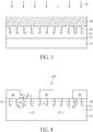
- FIG. 1 to FIG. 4 depict a method of adjusting an electron density of a 2DEG according to a first embodiment of the present invention.
- a gallium nitride (GaN) layer 10 is provided.
- an aluminum gallium nitride (Al x Ga 1-x N) layer 12 covers and contacts the gallium nitride layer 10.
- the gallium nitride layer 10 and the aluminum gallium nitride layer 12 can be formed by epitaxial processes.
- a tensile stress T1 is formed in the aluminum gallium nitride layer 12
- a compressive stress C1 is formed in the gallium nitride layer 10 after the aluminum gallium nitride layer 12 contacts the gallium nitride layer 10.
- piezoelectricity formed between the gallium nitride layer 10 and the aluminum gallium nitride layer 12 and a 2DEG 14 is formed in the gallium nitride layer 10.
- At least one trench 16 is formed in the aluminum gallium nitride layer 12. Based on different requirements, numerous trenches 16 can be formed. This embodiment takes eleven trenches as an example.
- a flowable chemical vapor deposition (FCVD) 18 is performed to form a silicon oxide layer 20 to fill the trenches 16 and cover the aluminum gallium nitride layer 12.
- a thermal process 22 is performed to cure the silicon oxide layer 20.
- the silicon oxide layer 20 is planarized to make a top surface of the silicon oxide layer 20 align with a top surface of the aluminum gallium nitride layer 12.
- the silicon oxide layer 20 may be planarized by a chemical mechanical planarization process.
- a source electrode 24, a gate electrode 26 and a drain electrode 28 are formed on the aluminum gallium nitride layer 12.
- the gate electrode 26 is between the source electrode 24 and the drain electrode 28.
- an HEMT 100 is completed.
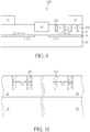
- FIG. 10 depicts a compressive stress in a silicon oxide layer and a tensile stress in a stressor. For the sake of clarity, only the gallium nitride layer 10, the aluminum gallium nitride layer 12, the silicon oxide layer 20 and a stressor 120 are shown, and other elements are omitted.
- the silicon oxide layer 20 is formed by the FCVD 18, the silicon oxide layer 20 includes a compressive stress C3. Therefore, the aluminum gallium nitride layer 12 around the silicon oxide layer 20 is influenced by the compressive stress C3 to contain a tensile stress T2.
- the tensile stress of the aluminum gallium nitride layer 12 becomes the tensile stress T1 pluses the tensile stress T2.
- the increase of the tensile stress of the aluminum gallium nitride layer 12 raises the piezoelectricity, thereby increasing the electron density of the 2DEG 14.
- the end result is that the operating efficiency of the HEMT 100 is also enhanced. At this point, a method of adjusting an electron density of a 2DEG is completed.
- FIG. 4 depicts an HEMT according to a second preferred embodiment of the present invention.
- the HEMT 100 is a normally-on HEMT.
- the HEMT 100 includes a gallium nitride layer 10.
- An aluminum gallium nitride layer 12 is disposed on the gallium nitride layer 10.
- the aluminum gallium nitride layer 12 includes a tensile stress T1.
- the gallium nitride layer 10 includes a compressive stress C1.
- a source electrode 24 and a drain electrode 28 are disposed on the aluminum gallium nitride layer 12.
- a gate electrode 26 is disposed on the aluminum gallium nitride layer 12 between the source electrode 24 and the drain electrode 28.
- At least one silicon oxide layer 20 is embedded in the aluminum gallium nitride layer 12.
- the thickness D1 of the silicon oxide layer 20 is not larger than the thickness of the aluminum gallium nitride layer 12.
- a top surface of the silicon oxide layer 20 is aligned with a top surface of the aluminum gallium nitride layer 12.
- the silicon oxide layer 20 can be disposed in the aluminum gallium nitride layer 12 directly under the source electrode 24, in the aluminum gallium nitride layer 12 directly under the drain electrode 28, or in the aluminum gallium nitride layer 12 between the aluminum gallium nitride layer 12 directly under the source electrode 24 and the aluminum gallium nitride layer 12 directly under the drain electrode 28.
- This embodiment takes numerous silicon oxide layers 20 disposed from the aluminum gallium nitride layer 12 directly under the source electrode 24 to the aluminum gallium nitride layer 12 directly under the drain electrode 28 as an example.
- the silicon oxide layer 20 is formed by the FCVD 18; therefore, the silicon oxide layer 20 contains a compressive stress. After the silicon oxide layer 20 is embedded into the aluminum gallium nitride layer 12, the tensile stress in the aluminum gallium nitride layer 12 can be increased.
- the aspect ratio of the silicon oxide layer is between 0.5 and 5.
- the gap G between the adjacent silicon oxide layers 20 is between 0.2 and 200 times of the width W1 of one of the silicon oxide layers 20.
- the thickness D1 of one of the silicon oxide layer 20 is about 50 nanometers.
- the width W1 of one of the silicon oxide layer 20 is between 10 and 100 nanometers.
- the gap G between the adjacent silicon oxide layers 20 is between 20 and 2000 nanometers. According to different sizes of the HEMT 100, the electron density of the 2DEG, the size, the gap, or the thickness of the silicon oxide layer 20 can be changed.
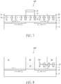
- FIG. 5 to FIG. 6 depict a method of adjusting an electron density of a 2DEG according to a third embodiment of the present invention, wherein like reference numerals are used to refer to like elements in the first preferred embodiment.
- a gallium nitride layer 10 is provided.
- an aluminum gallium nitride layer 12 is formed to cover and contact the gallium nitride layer 10.
- at least one trench 116 is formed in the aluminum gallium nitride layer 12.
- numerous trenches 116 are shown as an example.
- a chemical vapor deposition process 118 is performed to form a stressor 120 to fill the trenches 116.
- the stressor 120 can be silicon oxide, silicon nitride or other material layers which can contain stress. As shown in FIG.
- the stressor 120 is planarized to make a top surface of the stressor 120 align with a top surface of the aluminum gallium nitride layer 12.
- a source electrode 24, a gate electrode 26 and a drain electrode 28 are formed on the aluminum gallium nitride layer 12.
- the gate electrode 26 is between the source electrode 24 and the drain electrode 28.
- an HEMT 200 is completed.
- the stressor 120 contains a tensile stress T3; therefore, the aluminum gallium nitride layer 12 around the stressor 120 is influenced by the tensile stress T3 to contain a compressive stress C2. In this way, the tensile stress of the aluminum gallium nitride layer 12 becomes the tensile stress T1 minus the value of the compressive stress C2.
- the piezoelectricity is decreased, and the electron density of the 2DEG 14 is also decreased. At this point, another method of adjusting an electron density of the 2DEG is completed.
- the present invention utilizes stressors 120 to make the electron density of the 2DEG 14 decrease. When the electron density is lowered, the resistivity is raised. In this way, even when a high voltage is applied to the HEMT 200, the voltage is decreased slowly, and a sudden high current conduction can be prevented.
- FIG. 6 depicts an HEMT according to a fourth preferred embodiment of the present invention, wherein like reference numerals are used to refer to like elements in the first preferred embodiment.
- the HEMT 200 is a normally-on HEMT.
- the HEMT 200 includes a gallium nitride layer 10.
- An aluminum gallium nitride layer 12 is disposed on the gallium nitride layer 10.
- the aluminum gallium nitride layer 12 includes a tensile stress T1.
- the gallium nitride layer 10 includes a compressive stress C1.
- a source electrode 24 and a drain electrode 28 are disposed on the aluminum gallium nitride layer 12.
- a gate electrode 26 is disposed on the aluminum gallium nitride layer 12 between the source electrode 24 and the drain electrode 28.
- At least one stressor 120 is embedded in the aluminum gallium nitride layer 12.
- the stressor 120 decreases the tensile stress T1 in the aluminum gallium nitride layer 12.
- the thickness D2 of the stressor 120 is smaller than the thickness of the aluminum gallium nitride layer 12.
- a top surface of the stressor 120 is aligned with a top surface of the aluminum gallium nitride layer 12.
- the stressor 120 can be disposed in the aluminum gallium nitride layer 12 directly under the gate electrode 26, in the aluminum gallium nitride layer 12 directly under the drain electrode 28, or in the aluminum gallium nitride layer 12 between the aluminum gallium nitride layer 12 directly under the gate electrode 26 and the aluminum gallium nitride layer 12 directly under the drain electrode 28.
- the stressor 120 is preferably closer to the drain electrode 28 and farther from the gate electrode 26. This embodiment takes numerous stressors 120 disposed at the aluminum gallium nitride layer 12 closer to the drain electrode 28 as an example.
- the distance A between the gate electrode 26 and the drain electrode 28 is more than 233 times of a thickness D2 of the stressor 120.
- the ratio of the distance A to a width W2 of the stressor 116 is between 14 and 140.
- the thickness D2 of each of the stressors 120 is smaller than 30 nanometers.
- the width W2 of each of the stressors 120 is between 50 and 500 nanometers. According to different sizes of the HEMT 200 or the voltage applied to the HEMT 200, the size, or the thickness of the stressor 120 can be changed.
- FIG. 7 to FIG. 9 depict a method of adjusting an electron density of a 2DEG according to another preferred embodiment of the present invention, wherein like reference numerals are used to refer to like elements in the first preferred embodiment and the third preferred embodiment.
- the method of adjusting an electron density of a 2DEG of the present invention can be applied to normally-on HEMTs and normally-off HEMTs.
- the HEMT 300 is a normally-off HEMT.
- the difference between the HEMT 100 in FIG. 4 and the HEMT 300 in FIG. 7 is that the HEMT 300 includes a P-type gallium nitride layer 30.
- the normally-off HEMT liked the HEMT 300 can use the silicon oxide layer 20 shown in this embodiment to increase the electron density of the 2DEG 14, or use the stressor 120 shown in FIG. 6 to decrease the electron density of the 2DEG 14.
- the HEMT 400 is a normally-off HEMT.
- the difference between the HEMT 100 in FIG. 6 and the HEMT 400 in FIG. 8 is that the HEMT 400 includes a fluorine doped area 32 within the aluminum gallium nitride layer 12.
- the normally-off HEMT liked the HEMT 400 can use the stressor 120 shown in this embodiment to decrease the electron density of the 2DEG 14 or use the silicon oxide layer 20 shown in FIG. 4 to increase the electron density of the 2DEG 14.
- the HEMT 500 is a normally-off HEMT.
- the difference between the HEMT 100 in FIG. 6 and the HEMT 500 in FIG. 9 is that the gate electrode 26 of the HEMT 500 is embedded within the aluminum gallium nitride layer 12.
- the normally-off HEMT liked the HEMT 500 can use the stressor 120 shown in this embodiment to decrease the electron density of the 2DEG 14 or use the silicon oxide layer 20 shown in FIG. 4 to increase the electron density of the 2DEG 14.
- the present invention increases the electron density of the 2DEG by embedding the silicon oxide layer formed by the FCVD to raise the efficiency of the HEMT. Furthermore, the present invention decreases the electron density of the 2DEG by embedding stressors to increase the ability of the HEMT for sustaining high voltage.
Landscapes
- Engineering & Computer Science (AREA)
- Junction Field-Effect Transistors (AREA)
- Physics & Mathematics (AREA)
- Condensed Matter Physics & Semiconductors (AREA)
- General Physics & Mathematics (AREA)
- Manufacturing & Machinery (AREA)
- Computer Hardware Design (AREA)
- Microelectronics & Electronic Packaging (AREA)
- Power Engineering (AREA)
- Chemical & Material Sciences (AREA)
- Chemical Kinetics & Catalysis (AREA)
Applications Claiming Priority (1)
| Application Number | Priority Date | Filing Date | Title |
|---|---|---|---|
| CN201910553143.8A CN112133739B (zh) | 2019-06-25 | 2019-06-25 | 高电子迁移率晶体管和调整二维电子气体电子密度的方法 |
Publications (2)
| Publication Number | Publication Date |
|---|---|
| EP3758069A2 true EP3758069A2 (de) | 2020-12-30 |
| EP3758069A3 EP3758069A3 (de) | 2021-02-17 |
Family
ID=70227829
Family Applications (1)
| Application Number | Title | Priority Date | Filing Date |
|---|---|---|---|
| EP20168437.0A Pending EP3758069A3 (de) | 2019-06-25 | 2020-04-07 | Hemt und verfahren zum einstellen der elektronendichte eines 2deg |
Country Status (3)
| Country | Link |
|---|---|
| US (1) | US11239327B2 (de) |
| EP (1) | EP3758069A3 (de) |
| CN (1) | CN112133739B (de) |
Families Citing this family (15)
| Publication number | Priority date | Publication date | Assignee | Title |
|---|---|---|---|---|
| CN114520263A (zh) | 2020-11-19 | 2022-05-20 | 联华电子股份有限公司 | 半导体装置及半导体装置的制作方法 |
| CN114695503A (zh) | 2020-12-31 | 2022-07-01 | 联华电子股份有限公司 | 半导体结构 |
| CN115036366A (zh) | 2021-03-05 | 2022-09-09 | 联华电子股份有限公司 | 半导体装置及其制作方法 |
| CN115312596B (zh) | 2021-05-07 | 2025-11-21 | 联华电子股份有限公司 | 高电子迁移率晶体管及其制作方法 |
| CN115483197B (zh) | 2021-05-31 | 2025-12-05 | 联华电子股份有限公司 | 电容器结构以及其制作方法 |
| CN115621310B (zh) | 2021-07-16 | 2026-01-02 | 联华电子股份有限公司 | 半导体装置以及其制作方法 |
| CN115706081A (zh) | 2021-08-16 | 2023-02-17 | 联华电子股份有限公司 | 半导体结构及其制作方法 |
| US12002681B2 (en) | 2021-10-12 | 2024-06-04 | United Microelectronics Corp. | High electron mobility transistor and fabricating method of the same |
| CN116110963A (zh) | 2021-11-09 | 2023-05-12 | 联华电子股份有限公司 | 半导体装置以及其制作方法 |
| CN114242574B (zh) * | 2021-11-09 | 2024-10-29 | 上海华力集成电路制造有限公司 | 金属栅极上介质层刻蚀方法 |
| CN116153993A (zh) | 2021-11-23 | 2023-05-23 | 联华电子股份有限公司 | 半导体结构及其形成方法 |
| CN116960171A (zh) | 2022-04-12 | 2023-10-27 | 联华电子股份有限公司 | 半导体装置及其制造方法 |
| CN116978845A (zh) | 2022-04-22 | 2023-10-31 | 联芯集成电路制造(厦门)有限公司 | 半导体制作工艺 |
| TWI892010B (zh) | 2022-04-27 | 2025-08-01 | 聯華電子股份有限公司 | 半導體裝置以及其製作方法 |
| CN119997546B (zh) * | 2025-01-20 | 2025-12-30 | 西安电子科技大学 | 一种张应变高空穴迁移率场效应晶体管及其制备方法 |
Family Cites Families (14)
| Publication number | Priority date | Publication date | Assignee | Title |
|---|---|---|---|---|
| JP5093991B2 (ja) * | 2005-03-31 | 2012-12-12 | 住友電工デバイス・イノベーション株式会社 | 半導体装置 |
| US8497527B2 (en) * | 2008-03-12 | 2013-07-30 | Sensor Electronic Technology, Inc. | Device having active region with lower electron concentration |
| JP2011187654A (ja) * | 2010-03-08 | 2011-09-22 | Toyoda Gosei Co Ltd | Iii族窒化物半導体からなるhemt、およびその製造方法 |
| KR101051561B1 (ko) * | 2010-04-14 | 2011-07-22 | 삼성전기주식회사 | 질화물계 반도체 소자 및 그 제조 방법 |
| DE102010016993A1 (de) * | 2010-05-18 | 2011-11-24 | United Monolithic Semiconductors Gmbh | Halbleiter-Bauelement |
| US8884308B2 (en) * | 2011-11-29 | 2014-11-11 | Taiwan Semiconductor Manufacturing Company, Ltd. | High electron mobility transistor structure with improved breakdown voltage performance |
| US20140335666A1 (en) | 2013-05-13 | 2014-11-13 | The Government Of The United States Of America, As Represented By The Secretary Of The Navy | Growth of High-Performance III-Nitride Transistor Passivation Layer for GaN Electronics |
| CN104425267B (zh) * | 2013-08-27 | 2017-07-14 | 中芯国际集成电路制造(北京)有限公司 | 晶体管的形成方法 |
| US10121712B2 (en) * | 2015-04-06 | 2018-11-06 | Drexel University | Accelerated failure test of coupled device structures under direct current bias |
| CN106935641A (zh) * | 2015-12-31 | 2017-07-07 | 北京大学 | 高电子迁移率晶体管和存储器芯片 |
| CN106935643A (zh) * | 2015-12-31 | 2017-07-07 | 北京大学 | 高电子迁移率晶体管和存储器芯片 |
| CN105762184A (zh) * | 2016-04-27 | 2016-07-13 | 电子科技大学 | 一种具有半绝缘层的氮化镓基高电子迁移率晶体管 |
| EP3459118A4 (de) | 2016-05-17 | 2020-01-15 | The Government Of The United States Of America As The Secretary of The Navy | Beschädigungsfreie, plasmaunterstützte cvd-passivierung von algan/gan-transistoren mit hoher elektronenmobilität |
| WO2018004660A1 (en) | 2016-07-01 | 2018-01-04 | Intel Corporation | Gate stack design for gan e-mode transistor performance |
-
2019
- 2019-06-25 CN CN201910553143.8A patent/CN112133739B/zh active Active
- 2019-07-16 US US16/513,699 patent/US11239327B2/en active Active
-
2020
- 2020-04-07 EP EP20168437.0A patent/EP3758069A3/de active Pending
Also Published As
| Publication number | Publication date |
|---|---|
| CN112133739A (zh) | 2020-12-25 |
| US20200411649A1 (en) | 2020-12-31 |
| EP3758069A3 (de) | 2021-02-17 |
| CN112133739B (zh) | 2024-05-07 |
| US11239327B2 (en) | 2022-02-01 |
Similar Documents
| Publication | Publication Date | Title |
|---|---|---|
| US11239327B2 (en) | HEMT and method of adjusting electron density of 2DEG | |
| JP6173661B2 (ja) | Iii−窒化物デバイスの製造方法およびiii−窒化物デバイス | |
| CN111883588B (zh) | 用于hemt器件的侧壁钝化 | |
| KR101620987B1 (ko) | 갈륨 나이트라이드 완충층에서의 도펀트 확산 변조 | |
| US9406792B2 (en) | Semiconductor device having GaN-based layer | |
| JP2017201685A (ja) | Hfet装置のための保護絶縁体 | |
| KR101672396B1 (ko) | 4원계 질화물 전력반도체소자 및 이의 제조 방법 | |
| KR20110032845A (ko) | 전력 전자소자 및 그 제조방법 | |
| KR20190112523A (ko) | 이종접합 전계효과 트랜지스터 및 그 제조 방법 | |
| CN112216741B (zh) | 高电子迁移率晶体管的绝缘结构以及其制作方法 | |
| KR20120124101A (ko) | 고효율 질화계 이종접합 전계효과 트랜지스터 | |
| US9887267B2 (en) | Normally-off field effect transistor | |
| KR101200274B1 (ko) | 인헨스먼트 노멀리 오프 버티컬 질화물 반도체 소자 및 그 제조방법 | |
| US11935947B2 (en) | Enhancement mode high electron mobility transistor | |
| US12015076B2 (en) | HEMT and method of fabricating the same | |
| CN112490278B (zh) | 具有减少的缺陷的半导体外延结构 | |
| IT202300015876A1 (it) | Procedimento di fabbricazione di un dispositivo elettronico a semiconduttore integrante componenti elettronici diversi tra loro e dispositivo elettronico a semiconduttore | |
| WO2023184129A1 (en) | Semiconductor device and method for manufacturing the same | |
| KR102080744B1 (ko) | 질화물 반도체 소자 및 그 제조 방법 | |
| CN112397583B (zh) | 增强型高电子迁移率晶体管器件 | |
| WO2024040513A1 (en) | Semiconductor device and method for manufacturing the same | |
| KR101652403B1 (ko) | 전력 전자소자 및 그 제조방법 | |
| KR101622916B1 (ko) | 양성자 빔 조사에 의한 상시불통형 GaN계 트랜지스터 및 그 제조 방법 | |
| IT202300015885A1 (it) | Procedimento di fabbricazione di un dispositivo elettronico a semiconduttore integrante componenti elettronici diversi tra loro e dispositivo elettronico a semiconduttore | |
| KR20120012304A (ko) | 전력 전자소자 및 그 제조방법 |
Legal Events
| Date | Code | Title | Description |
|---|---|---|---|
| PUAI | Public reference made under article 153(3) epc to a published international application that has entered the european phase |
Free format text: ORIGINAL CODE: 0009012 |
|
| STAA | Information on the status of an ep patent application or granted ep patent |
Free format text: STATUS: THE APPLICATION HAS BEEN PUBLISHED |
|
| AK | Designated contracting states |
Kind code of ref document: A2 Designated state(s): AL AT BE BG CH CY CZ DE DK EE ES FI FR GB GR HR HU IE IS IT LI LT LU LV MC MK MT NL NO PL PT RO RS SE SI SK SM TR |
|
| AX | Request for extension of the european patent |
Extension state: BA ME |
|
| PUAL | Search report despatched |
Free format text: ORIGINAL CODE: 0009013 |
|
| AK | Designated contracting states |
Kind code of ref document: A3 Designated state(s): AL AT BE BG CH CY CZ DE DK EE ES FI FR GB GR HR HU IE IS IT LI LT LU LV MC MK MT NL NO PL PT RO RS SE SI SK SM TR |
|
| AX | Request for extension of the european patent |
Extension state: BA ME |
|
| RIC1 | Information provided on ipc code assigned before grant |
Ipc: H01L 29/207 20060101ALN20210113BHEP Ipc: H01L 21/337 20060101ALI20210113BHEP Ipc: H01L 29/10 20060101ALN20210113BHEP Ipc: H01L 21/338 20060101ALI20210113BHEP Ipc: H01L 29/06 20060101ALI20210113BHEP Ipc: H01L 29/423 20060101ALN20210113BHEP Ipc: H01L 29/20 20060101ALN20210113BHEP Ipc: H01L 29/778 20060101AFI20210113BHEP |
|
| STAA | Information on the status of an ep patent application or granted ep patent |
Free format text: STATUS: REQUEST FOR EXAMINATION WAS MADE |
|
| 17P | Request for examination filed |
Effective date: 20210708 |
|
| RBV | Designated contracting states (corrected) |
Designated state(s): AL AT BE BG CH CY CZ DE DK EE ES FI FR GB GR HR HU IE IS IT LI LT LU LV MC MK MT NL NO PL PT RO RS SE SI SK SM TR |
|
| STAA | Information on the status of an ep patent application or granted ep patent |
Free format text: STATUS: EXAMINATION IS IN PROGRESS |
|
| 17Q | First examination report despatched |
Effective date: 20221130 |
|
| RAP3 | Party data changed (applicant data changed or rights of an application transferred) |
Owner name: UNITED MICROELECTRONICS CORP. |