EP3757650B1 - Illumination system for sted optical microscope and sted optical microscope - Google Patents
Illumination system for sted optical microscope and sted optical microscope Download PDFInfo
- Publication number
- EP3757650B1 EP3757650B1 EP18934542.4A EP18934542A EP3757650B1 EP 3757650 B1 EP3757650 B1 EP 3757650B1 EP 18934542 A EP18934542 A EP 18934542A EP 3757650 B1 EP3757650 B1 EP 3757650B1
- Authority
- EP
- European Patent Office
- Prior art keywords
- light
- light beam
- optical
- illumination
- sted
- Prior art date
- Legal status (The legal status is an assumption and is not a legal conclusion. Google has not performed a legal analysis and makes no representation as to the accuracy of the status listed.)
- Active
Links
Images
Classifications
-
- G—PHYSICS
- G02—OPTICS
- G02B—OPTICAL ELEMENTS, SYSTEMS OR APPARATUS
- G02B21/00—Microscopes
- G02B21/0004—Microscopes specially adapted for specific applications
- G02B21/002—Scanning microscopes
- G02B21/0024—Confocal scanning microscopes (CSOMs) or confocal "macroscopes"; Accessories which are not restricted to use with CSOMs, e.g. sample holders
- G02B21/0032—Optical details of illumination, e.g. light-sources, pinholes, beam splitters, slits, fibers
-
- G—PHYSICS
- G02—OPTICS
- G02B—OPTICAL ELEMENTS, SYSTEMS OR APPARATUS
- G02B21/00—Microscopes
- G02B21/06—Means for illuminating specimens
-
- G—PHYSICS
- G02—OPTICS
- G02B—OPTICAL ELEMENTS, SYSTEMS OR APPARATUS
- G02B21/00—Microscopes
- G02B21/0004—Microscopes specially adapted for specific applications
- G02B21/002—Scanning microscopes
- G02B21/0024—Confocal scanning microscopes (CSOMs) or confocal "macroscopes"; Accessories which are not restricted to use with CSOMs, e.g. sample holders
- G02B21/0052—Optical details of the image generation
- G02B21/0076—Optical details of the image generation arrangements using fluorescence or luminescence
-
- G—PHYSICS
- G02—OPTICS
- G02B—OPTICAL ELEMENTS, SYSTEMS OR APPARATUS
- G02B27/00—Optical systems or apparatus not provided for by any of the groups G02B1/00 - G02B26/00, G02B30/00
- G02B27/58—Optics for apodization or superresolution; Optical synthetic aperture systems
Definitions
- the present disclosure relates to the technical field of microscopic imaging, and in particular to an illumination system for a STED optical microscope, and a STED optical microscope.
- a stimulated emission depletion (STED) microscope uses a beam of STED light to form a shell-shaped light spot, so that fluorescent molecules around an excitation light diffracted light spot are converted into a non-spontaneous-emission state through stimulated emission depletion, thereby achieving a spatial resolution superior to 50nm. Due to the plenoptic configuration, the image acquisition time is the same as that of a traditional confocal microscope, and there are no special requirements on sample preparation, so real-time imaging and dynamic tracking of the subcellular structures in living cells can be achieved.
- An object of the present disclosure is to at least solve one of the above-mentioned defects and shortcomings, and the object is achieved through the following technical solutions.
- the present disclosure provides an illumination system for a STED optical microscope, which includes an illumination light source, and an illumination light path composed of optical elements; after passing through the illumination light path, a light beam emitted from the illumination light source is focused and irradiated onto a sample to excite fluorescent substance in the sample to emit fluorescence;
- the illumination light path includes a first optical filter, a second optical filter, a polarization beam splitter, a first quarter-wave plate, a first dichroic element, an optical path delay unit, a phase plate, a second dichroic element and a second quarter-wave plate, which are arranged in sequence in a transmission direction of the light path; after the light beam emitted from the illumination light source is optically filtered by the first optical filter and the second optical filter, a first light beam and a second light beam each having a certain wavelength are obtained; the first light beam and the second light beam are respectively split by the polarization beam splitter to form linearly polarized lights which, after being reflected, are incident onto the first quarter
- the first light beam is excitation light
- the first light spot is a solid light spot
- the second light beam is depletion light relative to the first light beam
- the second light spot is a hollow light spot.
- the first optical filter is a neutral optical filter configured to adjust an intensity of a total laser light emitted from illumination light source;
- the second optical filter is a dual-band-pass optical filter configured to filter out the first light beam and the second light beam each having the certain wavelength, and adjust an intensity of the first light beam and an intensity of the second light beam, wherein the first optical filter and the second optical filter are arranged coaxially along the light path.
- the first quarter-wave plate is capable of converting the incident first light beam and second light beam from linearly polarized light into circularly polarized light, and is also capable of converting the incident first light beam and second light beam from circularly polarized light into linearly polarized light; the second quarter-wave plate is capable of converting linearly polarized light into circularly polarized light.
- the first dichroic element is a selective transmission medium film, the medium film is plated on an incident end of the optical path delay unit, and the medium film is capable of reflecting the incident first light beam and is capable of transmitting the incident second light beam;
- the second dichroic element is a dichroic sheet, and the dichroic sheet is capable of reflecting both the incident first light beam and second light beam and is capable of transmitting the fluorescence emitted from the sample.
- optical path delay unit is capable of causing optical delay in the second light beam.
- the phase plate is a reflective phase plate, which is arranged at a distal end of the optical path delay unit; the second light beam enters the optical path delay unit and is then incident onto the phase plate; after being reflected, the second light beam can return to an incident end of the optical path delay unit along the original light path; in addition, the phase plate is capable of modulating a wavefront of the incident second light beam.
- a beam expander for expanding and shaping the light beam emitted from the illumination light source is further provided between the illumination light source and the first optical filter.
- the present disclosure also provides a STED optical microscope including the illumination system for a STED optical microscope described above.
- the STED optical microscope further includes a microscopic imaging system and a fluorescence detection system, and the microscopic imaging system includes a microscopic objective lens; after passing through an illumination light path of the illumination system, a light beam emitted from the illumination light source is divided into two coaxial light beams, i.e., a first light beam and a second light beam; the first light beam and the second light beam are respectively converged by the microscopic objective lens and then irradiated onto a sample to excite fluorescent substance in the sample to emit fluorescence; the fluorescence enters the fluorescence detection system for detection after being converged by the microscopic objective lens; an optical axis of the first light beam and an optical axis of the second light beam are both coaxial with an optical axis of a detection light path of the fluorescence detection system.
- a third optical filter for filtering the fluorescence is provided between an exit end of the microscopic imaging system and the fluorescence detection system.
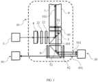
- FIG. 1 shows a schematic structural view of an illumination system for a STED optical microscope provided by an embodiment of the present disclosure.
- the illumination system is suitable for a STED optical microscope which includes an illumination system 10, a microscopic imaging system 20, and a fluorescence detection system 30.
- a light beam emitted from the illumination system 10 is focused by a microscopic objective lens of the microscopic imaging system 20 and then irradiated onto a sample to excite fluorescent substance in the sample to emit fluorescence, and the fluorescence of the sample is converged by the microscopic objective lens and then incident onto the fluorescence detection system 30 for detection.
- the illumination system for the STED optical microscope includes an illumination light source, and an illumination light path composed of optical elements.
- the illumination light source is a laser 1, which is capable of emitting a multi-wavelength laser light or a combination of multiple laser lights.
- the illumination light path includes a first optical filter 21, a second optical filter 22, a polarization beam splitter 3, a first quarter-wave plate 41, a first dichroic element 51, an optical path delay unit 6, a phase plate 7, a second dichroic element 52 and a second quarter-wave plate 42, which are arranged in sequence in a transmission direction of the light path; after the light beam emitted from the illumination light source 1 is optically filtered by the first optical filter 21 and the second optical filter 22, two beams of light, i.e., a first light beam 101 and a second light beam 102 are obtained; the first light beam 101 and the second light beam 102 are respectively split by the polarization beam splitter 3 and then incident onto the first quarter-wave plate 41 to produce circularly polarized light which is then incident onto the first dichroic element 51.
- the first light beam 101 incident onto the first dichroic element 51 sequentially passes through the first quarter-wave plate 41 to produce linearly polarized light, is transmitted through the polarization beam splitter 3, reflected by the second dichroic element 52, and converted by the second quarter-wave plate 42 into circularly polarized light to be incident onto the microscopic objective lens and converged, thus forming a first light spot at a focal plane of the objective lens;
- the second light beam 102 incident onto the first dichroic element 51 is incident onto the optical path delay unit 6 to produce optical delay;
- the second light beam 102 is sequentially exited from the optical path delay unit 6, transmitted through the first dichroic element 51 and the first quarter-wave plate 41 to produce linearly polarized light, transmitted through the polarization beam splitter 3, reflected by the second dichroic element 52, and converted by the second quarter-wave plate 42 into circularly polarized light, which is also
- the first light beam 101 is excitation light, which is used to excite fluorescence and perform fluorescence imaging on the sample;
- the second light beam 102 is depletion light relative to the first light beam 101, which is used to suppress fluorescence, and de-excite the fluorescent substance in the fluorescence emission state at a peripheral area of the first light spot so that the peripheral area no longer produces fluorescence.
- the first optical filter 21 is a neutral optical filter, and the first optical filter 21 can optically filter the light beam and adjust the intensity of the total laser light emitted from the illumination light source 1;
- the second optical filter 22 is a dual-band-pass optical filter, which is configured to optically filter out the first light beam 101 and the second light beam 102 of suitable wavelengths, and adjust the intensities of the two light beams.
- optical coating is applied to the second optical filter 22 to regulate the relative intensity of the excitation light and the depletion light.
- a beam expander 8 is provided between the laser 1 and the first optical filter 21, and the beam expander 8 can expand and shape the laser beam.
- the first optical filter 21 and the second optical filter 22 are arranged coaxially along the light path and coincide with an optical axis of the laser 1; an axis line of the beam expander 8 also coincides with the optical axis of the laser 1.
- the polarization beam splitter 3 can separate the incident light into two beams of linearly polarized light, polarization directions of which are perpendicular to each other, and which are reflected and transmitted respectively.
- the first light beam 101 and the second light beam 102 respectively pass through the polarization beam splitter 3 to form linearly polarized lights, wherein a P-polarized beam is discarded after being transmitted, and an S-polarized beam is reflected and then incident onto the first quarter-wave plate 41 and the first dichroic element 51 in sequence.
- the first quarter-wave plate 41 and the second quarter-wave plate 42 are configured to adjust polarization states of the light beams.
- the first quarter-wave plate 41 is capable of converting the incident first light beam 101 and second light beam 102 from linearly polarized light into circularly polarized light, and is also capable of converting the incident first light beam 101 and second light beam 102 from circularly polarized light into linearly polarized light;
- the second quarter-wave plate is capable of converting the first light beam 101 and the second light beam 102 from linearly polarized light into circularly polarized light.
- the first dichroic element 51 is a selective transmission medium film that can reflect the incident first light beam 101 and can transmit the second light beam 102.
- the second dichroic element 52 is a selective transmission dichroic sheet, which can reflect both the incident first light beam 101 and second light beam 102 and transmit the fluorescence emitted from the sample.
- the medium film of the first dichroic element 51 is plated on a surface of an incident end of the optical path delay unit 6, which not only can reduce the volume of the entire light path system and make the arrangement of optical elements more reasonable and compact, but also can reduce the influence of environmental factors such as temperature and vibration on the microscope.
- the optical path delay unit 6 is an optical glass having two ends strictly parallel with each other, and its length can be designed according to actual needs so as to generate the first light beam 101 and the second light beam 102 with suitable delay.
- the phase plate 7 is a reflective phase plate, which is arranged at a distal end of the optical path delay unit 6 and is perpendicular to an optical axis of the optical path delay unit 6 (a central line of the phase plate 7 coincides with the optical axis of the optical path delay unit 6), and the phase plate 7 is configured to modulate a wavefront and optical path of the depletion light and produce a hollow shell-shaped focal spot on a focal plane of the microscopic objective lens.
- phase modulated beam with a certain time delay which is strictly concentric with the excitation light and which is critical in the STED technology (the depletion light is converged by the objective lens to form the shell-shaped light spot), can be produced.
- the optical path delay unit 6 and the phase plate 7 may be of an integral structure or a split structure.
- the optical path delay unit 6 and the phase plate 7 are arranged as an integral structure, and the phase plate 7 is processed on a surface of an exit end of the optical path delay unit 6.
- the first light beam 101 is converted into circularly polarized light after passing through the first quarter-wave plate 41, and after being reflected by the first dichroic element 51, it forms linearly polarized light after passing through the first quarter-wave plate 41 again; the linearly polarized light is incident onto the polarization beam splitter 3 and transmitted.
- the second light beam 102 is converted into circularly polarized light after passing through the first quarter-wave plate 41, then transmitted through the first dichroic element 51 and enters the optical path delay unit 6 to generate optical delay, and is incident onto the phase plate 7 arranged at the distal end of the optical path delay unit 6; the second light beam 102 is wavefront-modulated and reflected by the phase plate 7 and then returns to the incident end of the optical path delay unit 6 along the original light path, and is transmitted through the first dichroic element 51 to the first quarter-wave plate 41 and converted into linearly polarized light which, after being transmitted through the polarization beam splitter 3, recombines with the first light beam 101 at the polarization beam splitter 3.
- first light beam 101 does not pass through the optical path delay unit 6 and the second light beam 102 passes through the optical path delay unit 6, there will be a fixed pulse time delay between the two, and the recombined first light beam 101 and second light beam 102 are coaxial.
- the recombined first light beam 101 and second light beam 102 are respectively reflected by the second dichroic element 52 and then pass through the second quarter-wave plate 42 so that linearly polarized lights are converted into circularly polarized lights, which then enter the microscopic imaging system to be converged and irradiated onto the sample by a focusing objective lens to form concentric light spots.
- the first light beam 101 is converged and irradiated onto the sample to form a solid light spot; the second light beam 102 is converged and irradiated onto the sample to form a hollow light spot.
- the first light beam 101 has a different wavelength from the second light beam 102, and after the coaxial transmission by the illumination light path, the first light beam 101 will excite fluorescence on the sample.
- the above solid light spot overlaps with the above hollow light spot.
- the solid light spot excites the fluorescent substance on the sample to emit fluorescence, and the hollow light spot suppresses the fluorescence emitted from the periphery of the fluorescent substance, so that only a middle point smaller than the diffraction limit emits fluorescence and is observed.
- the excited fluorescence is filtered by a third optical filter 9 and then received by the fluorescence detection system 30 for detection.
- the first quarter-wave plate 41 converts the light beam reflected by the polarization beam splitter 3 from linearly polarized light into circularly polarized light, and converts the circularly polarized light which is incident for the second time into linearly polarized light before it enters the polarization beam splitter 3 for transmission, thus achieving smooth transmission by the light path.
- the second quarter-wave plate 42 is used to set the excitation light entering the microscopic imaging system to circularly polarized light, thus obtaining a higher fluorescence excitation efficiency and a better shell-shaped focal spot.
- the polarization beam splitter 3 is connected to the first quarter-wave plate 41, and the first dichroic element 51 is plated on the surface of the optical path delay unit 6 to adjust the polarization properties of the excitation light and the depletion light and the transmission path of the light path; the second dichroic element 52 is connected to the second quarter-wave plate 42 to adjust the polarization state of the recombined excitation light and depletion light and change the propagation direction of light.
- the combined use of the polarization beam splitter 3 and the wave plates makes the light path compact, which is advantageous for achieving beam steering and beam polarization state control with fewer optical elements; moreover, various main optical elements can be combined into an integrated module by being bonded at end faces, which makes the device insensitive to temperature and environmental vibration while reducing the volumes of the devices, and improves the reliability.
- the third optical filter 9 is a fluorescence band-pass optical filter, which is arranged between the microscopic imaging system 20 and the fluorescence detection system 30.
- the fluorescence emitted from the sample passes through the third optical filter 9 to filter out other lights (including the scattered first light beam 101 and second light beam 102) than the fluorescence, and then enters the fluorescence detection system 30 for data collection.
- the third optical filter 9 is arranged on one side of the second dichroic element 52, and the second dichroic element 52 is configured as a lens capable of transmitting fluorescence, thereby ensuring that the fluorescence emitted from the sample directly enters the fluorescence detection system 30 for detection.
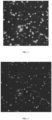
- FIG. 2 is an imaging view obtained by performing confocal imaging test on a sample of 40nm (diameter) fluorescent microspheres with a traditional confocal microscope
- FIG. 3 is an imaging view obtained by performing stimulated emission depletion (STED) microscopic imaging test on a sample of 40nm (diameter) fluorescent microspheres in the same area as FIG. 2 with the above STED optical microscope.
- STED stimulated emission depletion
- the illumination system for the STED optical microscope provided by the present disclosure can greatly improve the imaging resolution and obtain the effect of super-resolution imaging.
- the present disclosure also provides a STED optical microscope including the illumination system described above.
- the STED optical microscope further includes a microscopic imaging system 20 and a fluorescence detection system 30, and the microscopic imaging system 20 includes the microscopic objective lens; after passing through an illumination light path of the illumination system, a light beam emitted from the illumination light source is divided into two coaxial light beams, i.e., a first light beam 101 and a second light beam 102; the first light beam 101 and the second light beam 102 are respectively converged by the microscopic objective lens and then irradiated onto a sample to excite fluorescent substance in the sample to emit fluorescence; the fluorescence enters the fluorescence detection system 30 for detection after being converged by the microscopic objective lens; optical axes of the first light beam 101, the second light beam 102 and a detection light path of the fluorescence detection system 30 are all coaxial; and a focal plane of the above microscopic objective lens is perpendicular to each of the optical axes
- the illumination system for the STED optical microscope provided by the present disclosure can realize coaxial input and output of the excitation light, depletion light and confocal detection light path, and realize high-precision and long-time stable alignment of the excitation light spot and the STED shell-shaped light spot; at the same time, a physical adjustment of the mutual geometric relationship between unit devices and an inherent temperature and vibration instability of a mechanical adjustment mechanism are avoided, so that the STED instrument can work reliably and stably for a long time in various environments.
Landscapes
- Physics & Mathematics (AREA)
- General Physics & Mathematics (AREA)
- Optics & Photonics (AREA)
- Chemical & Material Sciences (AREA)
- Analytical Chemistry (AREA)
- Microscoopes, Condenser (AREA)
- Investigating, Analyzing Materials By Fluorescence Or Luminescence (AREA)
Applications Claiming Priority (2)
| Application Number | Priority Date | Filing Date | Title |
|---|---|---|---|
| CN201811125387.8A CN108957720B (zh) | 2018-09-26 | 2018-09-26 | 受激辐射损耗光学显微镜及其照明系统 |
| PCT/CN2018/121206 WO2020062609A1 (zh) | 2018-09-26 | 2018-12-14 | 用于sted光学显微镜的照明系统及sted光学显微镜 |
Publications (3)
| Publication Number | Publication Date |
|---|---|
| EP3757650A1 EP3757650A1 (en) | 2020-12-30 |
| EP3757650A4 EP3757650A4 (en) | 2021-12-15 |
| EP3757650B1 true EP3757650B1 (en) | 2024-01-03 |
Family
ID=64471900
Family Applications (1)
| Application Number | Title | Priority Date | Filing Date |
|---|---|---|---|
| EP18934542.4A Active EP3757650B1 (en) | 2018-09-26 | 2018-12-14 | Illumination system for sted optical microscope and sted optical microscope |
Country Status (5)
| Country | Link |
|---|---|
| US (1) | US11726309B2 (enExample) |
| EP (1) | EP3757650B1 (enExample) |
| JP (1) | JP7073523B2 (enExample) |
| CN (1) | CN108957720B (enExample) |
| WO (1) | WO2020062609A1 (enExample) |
Families Citing this family (16)
| Publication number | Priority date | Publication date | Assignee | Title |
|---|---|---|---|---|
| CN108957720B (zh) | 2018-09-26 | 2019-12-10 | 中国科学院化学研究所 | 受激辐射损耗光学显微镜及其照明系统 |
| CN111722388B (zh) * | 2019-03-18 | 2025-05-30 | 深圳市泽玖科技有限公司 | 一种三维微型内窥镜 |
| CN110068560B (zh) * | 2019-04-17 | 2021-08-06 | 深圳大学 | 一种受激辐射损耗超分辨成像系统及方法 |
| WO2020211018A1 (zh) * | 2019-04-17 | 2020-10-22 | 深圳大学 | 一种受激辐射损耗超分辨成像系统及方法 |
| US11271747B2 (en) | 2019-09-16 | 2022-03-08 | Lawrence Livermore National Security, Llc | Optical authentication of images |
| CN111855544B (zh) * | 2020-07-31 | 2021-11-26 | 上海微电子装备(集团)股份有限公司 | 一种荧光成像装置及其成像方法 |
| CN113484320B (zh) * | 2021-07-01 | 2024-08-02 | 西北大学 | 一种远场光学超薄片层成像系统及方法 |
| CN113866973B (zh) * | 2021-10-12 | 2023-10-03 | 桂林电子科技大学 | 一种基于多阶光纤模式复用的光纤sted显微镜 |
| CN114324156B (zh) * | 2021-11-18 | 2025-02-25 | 中国科学院化学研究所 | 受激辐射损耗显微镜及其显微成像系统 |
| CN114280802A (zh) * | 2021-12-28 | 2022-04-05 | 中国华录集团有限公司 | 一种单光源超分辨光存储光学系统 |
| CN114706208B (zh) * | 2022-02-18 | 2023-01-17 | 中国科学院化学研究所 | 受激辐射损耗光学显微镜及其显微成像系统 |
| CN115508994A (zh) * | 2022-09-14 | 2022-12-23 | 郑州思昆生物工程有限公司 | 一种显微成像系统 |
| CN115728869B (zh) * | 2022-11-15 | 2025-10-24 | 昂纳科技(深圳)集团股份有限公司 | 一种可调谐光滤波器 |
| CN117129426B (zh) * | 2023-08-08 | 2024-08-13 | 华东师范大学 | 一种超快时间分辨圆偏振发射光谱仪 |
| KR102899140B1 (ko) * | 2023-08-28 | 2025-12-10 | 고려대학교 산학협력단 | 편광 위상 현미경 시스템 |
| CN119804345A (zh) * | 2024-12-30 | 2025-04-11 | 长春理工大学中山研究院 | 一种对称式单lcvr偏振成像系统及成像方法 |
Family Cites Families (21)
| Publication number | Priority date | Publication date | Assignee | Title |
|---|---|---|---|---|
| JP2003262798A (ja) | 2002-03-12 | 2003-09-19 | Olympus Optical Co Ltd | 顕微鏡 |
| JP4334835B2 (ja) | 2002-08-28 | 2009-09-30 | 独立行政法人科学技術振興機構 | 顕微鏡 |
| DE102007025688A1 (de) * | 2007-06-01 | 2008-12-11 | MAX-PLANCK-Gesellschaft zur Förderung der Wissenschaften e.V. | Wellenlängen- oder polarisationssensitiver optischer Aufbau und dessen Verwendung |
| DE102010060121C5 (de) * | 2010-10-22 | 2023-09-28 | Leica Microsystems Cms Gmbh | SPIM-Mikroskop mit sequenziellem Lightsheet |
| JP5984351B2 (ja) | 2011-09-14 | 2016-09-06 | キヤノン株式会社 | 計測装置 |
| EP2776784B1 (en) * | 2011-11-08 | 2015-10-07 | Universite Laval | Method and system for improving resolution in laser imaging microscopy |
| CN102540439B (zh) | 2011-12-30 | 2013-10-30 | 哈尔滨工业大学 | 基于反射式液晶空间光调制器的共焦轴向扫描装置及共焦轴向扫描方法 |
| JP5988643B2 (ja) | 2012-03-26 | 2016-09-07 | キヤノン株式会社 | 計測装置、計測方法及び光学部品の製造方法 |
| GB201217171D0 (en) * | 2012-08-23 | 2012-11-07 | Isis Innovation | Stimulated emission depletion microscopy |
| CN103257130B (zh) | 2013-05-31 | 2015-04-01 | 中国科学院苏州生物医学工程技术研究所 | 受激辐射损耗显微成像系统 |
| ES2897575T3 (es) * | 2013-06-03 | 2022-03-01 | Lumicks Dsm Holding B V | Método y sistema para formar imágenes de una hebra molecular |
| JP6613552B2 (ja) | 2013-09-09 | 2019-12-04 | 株式会社ニコン | 超解像観察装置及び超解像観察方法 |
| CN103616330A (zh) | 2013-11-18 | 2014-03-05 | 中国科学院化学研究所 | 基于超连续产生的宽带激光光源激发的超分辨sted显微成像系统 |
| US10247672B2 (en) * | 2014-09-29 | 2019-04-02 | Howard Hughes Medical Institute | Non-linear structured illumination microscopy |
| WO2017174100A1 (de) * | 2016-04-08 | 2017-10-12 | Universität Heidelberg | Parallelisierung des sted-mikroskopieverfahrens |
| DE102016211374A1 (de) * | 2016-06-24 | 2017-12-28 | Carl Zeiss Microscopy Gmbh | Mikroskopieverfahren unter Nutzung zeitlicher Fokusmodulation und Mikroskop |
| US9880377B1 (en) * | 2016-09-09 | 2018-01-30 | Photonicsys Ltd. | Multiple wavelengths real time phase shift interference microscopy |
| CN106841149B (zh) * | 2017-03-17 | 2021-05-28 | 王富 | 受激辐射损耗显微装置 |
| CN107329245B (zh) * | 2017-07-06 | 2023-05-05 | 中国科学院西安光学精密机械研究所 | 基于径向偏振调制的干涉式结构光照明显微镜系统与方法 |
| CN108121059B (zh) * | 2017-11-18 | 2022-01-28 | 苏州国科医工科技发展(集团)有限公司 | 一种基于结构光照明的sted并行显微成像系统 |
| CN108957720B (zh) * | 2018-09-26 | 2019-12-10 | 中国科学院化学研究所 | 受激辐射损耗光学显微镜及其照明系统 |
-
2018
- 2018-09-26 CN CN201811125387.8A patent/CN108957720B/zh active Active
- 2018-12-14 US US17/043,615 patent/US11726309B2/en active Active
- 2018-12-14 JP JP2020551913A patent/JP7073523B2/ja active Active
- 2018-12-14 WO PCT/CN2018/121206 patent/WO2020062609A1/zh not_active Ceased
- 2018-12-14 EP EP18934542.4A patent/EP3757650B1/en active Active
Also Published As
| Publication number | Publication date |
|---|---|
| CN108957720A (zh) | 2018-12-07 |
| EP3757650A4 (en) | 2021-12-15 |
| JP7073523B2 (ja) | 2022-05-23 |
| CN108957720B (zh) | 2019-12-10 |
| US20210018736A1 (en) | 2021-01-21 |
| EP3757650A1 (en) | 2020-12-30 |
| WO2020062609A1 (zh) | 2020-04-02 |
| JP2021516794A (ja) | 2021-07-08 |
| US11726309B2 (en) | 2023-08-15 |
Similar Documents
| Publication | Publication Date | Title |
|---|---|---|
| EP3757650B1 (en) | Illumination system for sted optical microscope and sted optical microscope | |
| CN107941763B (zh) | 一种共轴三维受激辐射损耗超分辨显微成像方法和装置 | |
| CN106970055B (zh) | 一种三维荧光差分超分辨显微方法及装置 | |
| CN108303806B (zh) | 一种深度成像超分辨显微成像系统 | |
| CN108072970B (zh) | 光镊光片显微成像装置和方法 | |
| CN103698309B (zh) | 基于可调谐激光的sted超分辨显微镜 | |
| CN110568731B (zh) | 一种超衍射极限焦斑阵列生成装置 | |
| CN110632045A (zh) | 一种产生并行超分辨焦斑的方法和装置 | |
| CN109632756A (zh) | 一种基于并行光斑扫描的实时荧光辐射微分超分辨显微方法与装置 | |
| CN108020505B (zh) | 变焦共聚焦光镊显微成像装置和方法 | |
| CN109358030B (zh) | 一种具有自动对准功能的多色超分辨显微镜系统 | |
| CN110794561A (zh) | 一种便于阵列应用的显微镜 | |
| CN113325563B (zh) | 一种具有大视场的多色三维超分辨膨胀显微镜系统 | |
| CN111504970B (zh) | 一种镜面辅助三维超分辨显微成像系统及方法 | |
| CN107703616A (zh) | 多通道激光输出设备和荧光显微镜 | |
| CN109283674A (zh) | 一种荧光差分显微镜光路装置 | |
| CN116953920A (zh) | 一种激光扫描器及激光共聚焦显微镜 | |
| CN108051414A (zh) | 变焦光镊双光子显微成像装置和方法 | |
| CN111879737A (zh) | 一种产生高通量超衍射极限焦斑的装置和方法 | |
| CN218974142U (zh) | 一种多波段结构光显微成像系统 | |
| CN105929526B (zh) | 一种体全息还原扫描光束的sted超分辨显微系统及显微方法 | |
| CN114324156B (zh) | 受激辐射损耗显微镜及其显微成像系统 | |
| CN114706208B (zh) | 受激辐射损耗光学显微镜及其显微成像系统 | |
| CN205750086U (zh) | 一种体全息还原扫描光束的sted超分辨显微系统 | |
| CN117607114A (zh) | 一种基于偏振干涉的结构光照明多通道层析成像系统 |
Legal Events
| Date | Code | Title | Description |
|---|---|---|---|
| STAA | Information on the status of an ep patent application or granted ep patent |
Free format text: STATUS: THE INTERNATIONAL PUBLICATION HAS BEEN MADE |
|
| PUAI | Public reference made under article 153(3) epc to a published international application that has entered the european phase |
Free format text: ORIGINAL CODE: 0009012 |
|
| STAA | Information on the status of an ep patent application or granted ep patent |
Free format text: STATUS: REQUEST FOR EXAMINATION WAS MADE |
|
| 17P | Request for examination filed |
Effective date: 20200924 |
|
| AK | Designated contracting states |
Kind code of ref document: A1 Designated state(s): AL AT BE BG CH CY CZ DE DK EE ES FI FR GB GR HR HU IE IS IT LI LT LU LV MC MK MT NL NO PL PT RO RS SE SI SK SM TR |
|
| AX | Request for extension of the european patent |
Extension state: BA ME |
|
| A4 | Supplementary search report drawn up and despatched |
Effective date: 20211111 |
|
| RIC1 | Information provided on ipc code assigned before grant |
Ipc: G02B 27/58 20060101ALI20211105BHEP Ipc: G02B 21/00 20060101ALI20211105BHEP Ipc: G02B 21/06 20060101AFI20211105BHEP |
|
| DAV | Request for validation of the european patent (deleted) | ||
| DAX | Request for extension of the european patent (deleted) | ||
| GRAP | Despatch of communication of intention to grant a patent |
Free format text: ORIGINAL CODE: EPIDOSNIGR1 |
|
| STAA | Information on the status of an ep patent application or granted ep patent |
Free format text: STATUS: GRANT OF PATENT IS INTENDED |
|
| INTG | Intention to grant announced |
Effective date: 20230925 |
|
| GRAS | Grant fee paid |
Free format text: ORIGINAL CODE: EPIDOSNIGR3 |
|
| GRAA | (expected) grant |
Free format text: ORIGINAL CODE: 0009210 |
|
| STAA | Information on the status of an ep patent application or granted ep patent |
Free format text: STATUS: THE PATENT HAS BEEN GRANTED |
|
| AK | Designated contracting states |
Kind code of ref document: B1 Designated state(s): AL AT BE BG CH CY CZ DE DK EE ES FI FR GB GR HR HU IE IS IT LI LT LU LV MC MK MT NL NO PL PT RO RS SE SI SK SM TR |
|
| REG | Reference to a national code |
Ref country code: GB Ref legal event code: FG4D |
|
| REG | Reference to a national code |
Ref country code: CH Ref legal event code: EP |
|
| REG | Reference to a national code |
Ref country code: DE Ref legal event code: R096 Ref document number: 602018063842 Country of ref document: DE |
|
| REG | Reference to a national code |
Ref country code: IE Ref legal event code: FG4D |
|
| REG | Reference to a national code |
Ref country code: DE Ref legal event code: R081 Ref document number: 602018063842 Country of ref document: DE Owner name: INNOVATIVE SEMICONDUCTOR SUBSTRATE TECHNOLOGY , CN Free format text: FORMER OWNER: INSTITUTE OF CHEMISTRY, CHINESE ACADEMY OF SCIENCES, BEIJING, CN |
|
| RAP2 | Party data changed (patent owner data changed or rights of a patent transferred) |
Owner name: INNOVATIVE SEMICONDUCTOR SUBSTRATE TECHNOLOGY CO., LTD. |
|
| REG | Reference to a national code |
Ref country code: LT Ref legal event code: MG9D |
|
| PG25 | Lapsed in a contracting state [announced via postgrant information from national office to epo] |
Ref country code: ES Free format text: LAPSE BECAUSE OF FAILURE TO SUBMIT A TRANSLATION OF THE DESCRIPTION OR TO PAY THE FEE WITHIN THE PRESCRIBED TIME-LIMIT Effective date: 20240103 |
|
| PG25 | Lapsed in a contracting state [announced via postgrant information from national office to epo] |
Ref country code: ES Free format text: LAPSE BECAUSE OF FAILURE TO SUBMIT A TRANSLATION OF THE DESCRIPTION OR TO PAY THE FEE WITHIN THE PRESCRIBED TIME-LIMIT Effective date: 20240103 |
|
| REG | Reference to a national code |
Ref country code: NL Ref legal event code: MP Effective date: 20240103 |
|
| REG | Reference to a national code |
Ref country code: AT Ref legal event code: MK05 Ref document number: 1647387 Country of ref document: AT Kind code of ref document: T Effective date: 20240103 |
|
| PG25 | Lapsed in a contracting state [announced via postgrant information from national office to epo] |
Ref country code: NL Free format text: LAPSE BECAUSE OF FAILURE TO SUBMIT A TRANSLATION OF THE DESCRIPTION OR TO PAY THE FEE WITHIN THE PRESCRIBED TIME-LIMIT Effective date: 20240103 |
|
| PG25 | Lapsed in a contracting state [announced via postgrant information from national office to epo] |
Ref country code: NL Free format text: LAPSE BECAUSE OF FAILURE TO SUBMIT A TRANSLATION OF THE DESCRIPTION OR TO PAY THE FEE WITHIN THE PRESCRIBED TIME-LIMIT Effective date: 20240103 |
|
| PG25 | Lapsed in a contracting state [announced via postgrant information from national office to epo] |
Ref country code: IS Free format text: LAPSE BECAUSE OF FAILURE TO SUBMIT A TRANSLATION OF THE DESCRIPTION OR TO PAY THE FEE WITHIN THE PRESCRIBED TIME-LIMIT Effective date: 20240503 |
|
| PG25 | Lapsed in a contracting state [announced via postgrant information from national office to epo] |
Ref country code: LT Free format text: LAPSE BECAUSE OF FAILURE TO SUBMIT A TRANSLATION OF THE DESCRIPTION OR TO PAY THE FEE WITHIN THE PRESCRIBED TIME-LIMIT Effective date: 20240103 |
|
| PG25 | Lapsed in a contracting state [announced via postgrant information from national office to epo] |
Ref country code: GR Free format text: LAPSE BECAUSE OF FAILURE TO SUBMIT A TRANSLATION OF THE DESCRIPTION OR TO PAY THE FEE WITHIN THE PRESCRIBED TIME-LIMIT Effective date: 20240404 |
|
| PG25 | Lapsed in a contracting state [announced via postgrant information from national office to epo] |
Ref country code: HR Free format text: LAPSE BECAUSE OF FAILURE TO SUBMIT A TRANSLATION OF THE DESCRIPTION OR TO PAY THE FEE WITHIN THE PRESCRIBED TIME-LIMIT Effective date: 20240103 Ref country code: RS Free format text: LAPSE BECAUSE OF FAILURE TO SUBMIT A TRANSLATION OF THE DESCRIPTION OR TO PAY THE FEE WITHIN THE PRESCRIBED TIME-LIMIT Effective date: 20240403 |
|
| PG25 | Lapsed in a contracting state [announced via postgrant information from national office to epo] |
Ref country code: CZ Free format text: LAPSE BECAUSE OF FAILURE TO SUBMIT A TRANSLATION OF THE DESCRIPTION OR TO PAY THE FEE WITHIN THE PRESCRIBED TIME-LIMIT Effective date: 20240103 Ref country code: AT Free format text: LAPSE BECAUSE OF FAILURE TO SUBMIT A TRANSLATION OF THE DESCRIPTION OR TO PAY THE FEE WITHIN THE PRESCRIBED TIME-LIMIT Effective date: 20240103 |
|
| PG25 | Lapsed in a contracting state [announced via postgrant information from national office to epo] |
Ref country code: RS Free format text: LAPSE BECAUSE OF FAILURE TO SUBMIT A TRANSLATION OF THE DESCRIPTION OR TO PAY THE FEE WITHIN THE PRESCRIBED TIME-LIMIT Effective date: 20240403 Ref country code: NO Free format text: LAPSE BECAUSE OF FAILURE TO SUBMIT A TRANSLATION OF THE DESCRIPTION OR TO PAY THE FEE WITHIN THE PRESCRIBED TIME-LIMIT Effective date: 20240403 Ref country code: LT Free format text: LAPSE BECAUSE OF FAILURE TO SUBMIT A TRANSLATION OF THE DESCRIPTION OR TO PAY THE FEE WITHIN THE PRESCRIBED TIME-LIMIT Effective date: 20240103 Ref country code: IS Free format text: LAPSE BECAUSE OF FAILURE TO SUBMIT A TRANSLATION OF THE DESCRIPTION OR TO PAY THE FEE WITHIN THE PRESCRIBED TIME-LIMIT Effective date: 20240503 Ref country code: HR Free format text: LAPSE BECAUSE OF FAILURE TO SUBMIT A TRANSLATION OF THE DESCRIPTION OR TO PAY THE FEE WITHIN THE PRESCRIBED TIME-LIMIT Effective date: 20240103 Ref country code: GR Free format text: LAPSE BECAUSE OF FAILURE TO SUBMIT A TRANSLATION OF THE DESCRIPTION OR TO PAY THE FEE WITHIN THE PRESCRIBED TIME-LIMIT Effective date: 20240404 Ref country code: CZ Free format text: LAPSE BECAUSE OF FAILURE TO SUBMIT A TRANSLATION OF THE DESCRIPTION OR TO PAY THE FEE WITHIN THE PRESCRIBED TIME-LIMIT Effective date: 20240103 Ref country code: BG Free format text: LAPSE BECAUSE OF FAILURE TO SUBMIT A TRANSLATION OF THE DESCRIPTION OR TO PAY THE FEE WITHIN THE PRESCRIBED TIME-LIMIT Effective date: 20240103 Ref country code: AT Free format text: LAPSE BECAUSE OF FAILURE TO SUBMIT A TRANSLATION OF THE DESCRIPTION OR TO PAY THE FEE WITHIN THE PRESCRIBED TIME-LIMIT Effective date: 20240103 |
|
| PG25 | Lapsed in a contracting state [announced via postgrant information from national office to epo] |
Ref country code: PT Free format text: LAPSE BECAUSE OF FAILURE TO SUBMIT A TRANSLATION OF THE DESCRIPTION OR TO PAY THE FEE WITHIN THE PRESCRIBED TIME-LIMIT Effective date: 20240503 Ref country code: PL Free format text: LAPSE BECAUSE OF FAILURE TO SUBMIT A TRANSLATION OF THE DESCRIPTION OR TO PAY THE FEE WITHIN THE PRESCRIBED TIME-LIMIT Effective date: 20240103 |
|
| PG25 | Lapsed in a contracting state [announced via postgrant information from national office to epo] |
Ref country code: SE Free format text: LAPSE BECAUSE OF FAILURE TO SUBMIT A TRANSLATION OF THE DESCRIPTION OR TO PAY THE FEE WITHIN THE PRESCRIBED TIME-LIMIT Effective date: 20240103 Ref country code: PT Free format text: LAPSE BECAUSE OF FAILURE TO SUBMIT A TRANSLATION OF THE DESCRIPTION OR TO PAY THE FEE WITHIN THE PRESCRIBED TIME-LIMIT Effective date: 20240503 Ref country code: PL Free format text: LAPSE BECAUSE OF FAILURE TO SUBMIT A TRANSLATION OF THE DESCRIPTION OR TO PAY THE FEE WITHIN THE PRESCRIBED TIME-LIMIT Effective date: 20240103 Ref country code: LV Free format text: LAPSE BECAUSE OF FAILURE TO SUBMIT A TRANSLATION OF THE DESCRIPTION OR TO PAY THE FEE WITHIN THE PRESCRIBED TIME-LIMIT Effective date: 20240103 |
|
| REG | Reference to a national code |
Ref country code: DE Ref legal event code: R097 Ref document number: 602018063842 Country of ref document: DE |
|
| PG25 | Lapsed in a contracting state [announced via postgrant information from national office to epo] |
Ref country code: DK Free format text: LAPSE BECAUSE OF FAILURE TO SUBMIT A TRANSLATION OF THE DESCRIPTION OR TO PAY THE FEE WITHIN THE PRESCRIBED TIME-LIMIT Effective date: 20240103 |
|
| PG25 | Lapsed in a contracting state [announced via postgrant information from national office to epo] |
Ref country code: SM Free format text: LAPSE BECAUSE OF FAILURE TO SUBMIT A TRANSLATION OF THE DESCRIPTION OR TO PAY THE FEE WITHIN THE PRESCRIBED TIME-LIMIT Effective date: 20240103 |
|
| PG25 | Lapsed in a contracting state [announced via postgrant information from national office to epo] |
Ref country code: EE Free format text: LAPSE BECAUSE OF FAILURE TO SUBMIT A TRANSLATION OF THE DESCRIPTION OR TO PAY THE FEE WITHIN THE PRESCRIBED TIME-LIMIT Effective date: 20240103 |
|
| PG25 | Lapsed in a contracting state [announced via postgrant information from national office to epo] |
Ref country code: SK Free format text: LAPSE BECAUSE OF FAILURE TO SUBMIT A TRANSLATION OF THE DESCRIPTION OR TO PAY THE FEE WITHIN THE PRESCRIBED TIME-LIMIT Effective date: 20240103 |
|
| PG25 | Lapsed in a contracting state [announced via postgrant information from national office to epo] |
Ref country code: SM Free format text: LAPSE BECAUSE OF FAILURE TO SUBMIT A TRANSLATION OF THE DESCRIPTION OR TO PAY THE FEE WITHIN THE PRESCRIBED TIME-LIMIT Effective date: 20240103 Ref country code: SK Free format text: LAPSE BECAUSE OF FAILURE TO SUBMIT A TRANSLATION OF THE DESCRIPTION OR TO PAY THE FEE WITHIN THE PRESCRIBED TIME-LIMIT Effective date: 20240103 Ref country code: RO Free format text: LAPSE BECAUSE OF FAILURE TO SUBMIT A TRANSLATION OF THE DESCRIPTION OR TO PAY THE FEE WITHIN THE PRESCRIBED TIME-LIMIT Effective date: 20240103 Ref country code: EE Free format text: LAPSE BECAUSE OF FAILURE TO SUBMIT A TRANSLATION OF THE DESCRIPTION OR TO PAY THE FEE WITHIN THE PRESCRIBED TIME-LIMIT Effective date: 20240103 Ref country code: DK Free format text: LAPSE BECAUSE OF FAILURE TO SUBMIT A TRANSLATION OF THE DESCRIPTION OR TO PAY THE FEE WITHIN THE PRESCRIBED TIME-LIMIT Effective date: 20240103 |
|
| PLBE | No opposition filed within time limit |
Free format text: ORIGINAL CODE: 0009261 |
|
| STAA | Information on the status of an ep patent application or granted ep patent |
Free format text: STATUS: NO OPPOSITION FILED WITHIN TIME LIMIT |
|
| PG25 | Lapsed in a contracting state [announced via postgrant information from national office to epo] |
Ref country code: IT Free format text: LAPSE BECAUSE OF FAILURE TO SUBMIT A TRANSLATION OF THE DESCRIPTION OR TO PAY THE FEE WITHIN THE PRESCRIBED TIME-LIMIT Effective date: 20240103 |
|
| 26N | No opposition filed |
Effective date: 20241007 |
|
| PG25 | Lapsed in a contracting state [announced via postgrant information from national office to epo] |
Ref country code: IT Free format text: LAPSE BECAUSE OF FAILURE TO SUBMIT A TRANSLATION OF THE DESCRIPTION OR TO PAY THE FEE WITHIN THE PRESCRIBED TIME-LIMIT Effective date: 20240103 |
|
| PGFP | Annual fee paid to national office [announced via postgrant information from national office to epo] |
Ref country code: DE Payment date: 20241210 Year of fee payment: 7 |
|
| PGFP | Annual fee paid to national office [announced via postgrant information from national office to epo] |
Ref country code: GB Payment date: 20241227 Year of fee payment: 7 |
|
| PGFP | Annual fee paid to national office [announced via postgrant information from national office to epo] |
Ref country code: FR Payment date: 20241224 Year of fee payment: 7 |
|
| REG | Reference to a national code |
Ref country code: DE Ref legal event code: R082 Ref document number: 602018063842 Country of ref document: DE Representative=s name: PLASSERAUD IP GMBH, DE |
|
| PG25 | Lapsed in a contracting state [announced via postgrant information from national office to epo] |
Ref country code: SI Free format text: LAPSE BECAUSE OF FAILURE TO SUBMIT A TRANSLATION OF THE DESCRIPTION OR TO PAY THE FEE WITHIN THE PRESCRIBED TIME-LIMIT Effective date: 20240103 |
|
| PG25 | Lapsed in a contracting state [announced via postgrant information from national office to epo] |
Ref country code: MC Free format text: LAPSE BECAUSE OF FAILURE TO SUBMIT A TRANSLATION OF THE DESCRIPTION OR TO PAY THE FEE WITHIN THE PRESCRIBED TIME-LIMIT Effective date: 20240103 |
|
| REG | Reference to a national code |
Ref country code: CH Ref legal event code: PL |
|
| PG25 | Lapsed in a contracting state [announced via postgrant information from national office to epo] |
Ref country code: LU Free format text: LAPSE BECAUSE OF NON-PAYMENT OF DUE FEES Effective date: 20241214 |
|
| PG25 | Lapsed in a contracting state [announced via postgrant information from national office to epo] |
Ref country code: FI Free format text: LAPSE BECAUSE OF FAILURE TO SUBMIT A TRANSLATION OF THE DESCRIPTION OR TO PAY THE FEE WITHIN THE PRESCRIBED TIME-LIMIT Effective date: 20240103 |
|
| REG | Reference to a national code |
Ref country code: BE Ref legal event code: MM Effective date: 20241231 |
|
| PG25 | Lapsed in a contracting state [announced via postgrant information from national office to epo] |
Ref country code: BE Free format text: LAPSE BECAUSE OF NON-PAYMENT OF DUE FEES Effective date: 20241231 |
|
| PG25 | Lapsed in a contracting state [announced via postgrant information from national office to epo] |
Ref country code: CH Free format text: LAPSE BECAUSE OF NON-PAYMENT OF DUE FEES Effective date: 20241231 |
|
| PG25 | Lapsed in a contracting state [announced via postgrant information from national office to epo] |
Ref country code: IE Free format text: LAPSE BECAUSE OF NON-PAYMENT OF DUE FEES Effective date: 20241214 |