EP3755672B1 - Organomodifizierter metalloxid- oder metalloidoxid-polymerfilm - Google Patents
Organomodifizierter metalloxid- oder metalloidoxid-polymerfilm Download PDFInfo
- Publication number
- EP3755672B1 EP3755672B1 EP19706616.0A EP19706616A EP3755672B1 EP 3755672 B1 EP3755672 B1 EP 3755672B1 EP 19706616 A EP19706616 A EP 19706616A EP 3755672 B1 EP3755672 B1 EP 3755672B1
- Authority
- EP
- European Patent Office
- Prior art keywords
- metal
- precursor composition
- solution
- metalloid
- added
- Prior art date
- Legal status (The legal status is an assumption and is not a legal conclusion. Google has not performed a legal analysis and makes no representation as to the accuracy of the status listed.)
- Active
Links
Images


Classifications
-
- C—CHEMISTRY; METALLURGY
- C09—DYES; PAINTS; POLISHES; NATURAL RESINS; ADHESIVES; COMPOSITIONS NOT OTHERWISE PROVIDED FOR; APPLICATIONS OF MATERIALS NOT OTHERWISE PROVIDED FOR
- C09D—COATING COMPOSITIONS, e.g. PAINTS, VARNISHES OR LACQUERS; FILLING PASTES; CHEMICAL PAINT OR INK REMOVERS; INKS; CORRECTING FLUIDS; WOODSTAINS; PASTES OR SOLIDS FOR COLOURING OR PRINTING; USE OF MATERIALS THEREFOR
- C09D133/00—Coating compositions based on homopolymers or copolymers of compounds having one or more unsaturated aliphatic radicals, each having only one carbon-to-carbon double bond, and at least one being terminated by only one carboxyl radical, or of salts, anhydrides, esters, amides, imides, or nitriles thereof; Coating compositions based on derivatives of such polymers
- C09D133/04—Homopolymers or copolymers of esters
- C09D133/14—Homopolymers or copolymers of esters of esters containing halogen, nitrogen, sulfur or oxygen atoms in addition to the carboxy oxygen
-
- C—CHEMISTRY; METALLURGY
- C09—DYES; PAINTS; POLISHES; NATURAL RESINS; ADHESIVES; COMPOSITIONS NOT OTHERWISE PROVIDED FOR; APPLICATIONS OF MATERIALS NOT OTHERWISE PROVIDED FOR
- C09D—COATING COMPOSITIONS, e.g. PAINTS, VARNISHES OR LACQUERS; FILLING PASTES; CHEMICAL PAINT OR INK REMOVERS; INKS; CORRECTING FLUIDS; WOODSTAINS; PASTES OR SOLIDS FOR COLOURING OR PRINTING; USE OF MATERIALS THEREFOR
- C09D183/00—Coating compositions based on macromolecular compounds obtained by reactions forming in the main chain of the macromolecule a linkage containing silicon, with or without sulfur, nitrogen, oxygen, or carbon only; Coating compositions based on derivatives of such polymers
- C09D183/14—Coating compositions based on macromolecular compounds obtained by reactions forming in the main chain of the macromolecule a linkage containing silicon, with or without sulfur, nitrogen, oxygen, or carbon only; Coating compositions based on derivatives of such polymers in which at least two but not all the silicon atoms are connected by linkages other than oxygen atoms
-
- C—CHEMISTRY; METALLURGY
- C03—GLASS; MINERAL OR SLAG WOOL
- C03C—CHEMICAL COMPOSITION OF GLASSES, GLAZES OR VITREOUS ENAMELS; SURFACE TREATMENT OF GLASS; SURFACE TREATMENT OF FIBRES OR FILAMENTS MADE FROM GLASS, MINERALS OR SLAGS; JOINING GLASS TO GLASS OR OTHER MATERIALS
- C03C17/00—Surface treatment of glass, not in the form of fibres or filaments, by coating
- C03C17/28—Surface treatment of glass, not in the form of fibres or filaments, by coating with organic material
- C03C17/30—Surface treatment of glass, not in the form of fibres or filaments, by coating with organic material with silicon-containing compounds
-
- C—CHEMISTRY; METALLURGY
- C03—GLASS; MINERAL OR SLAG WOOL
- C03C—CHEMICAL COMPOSITION OF GLASSES, GLAZES OR VITREOUS ENAMELS; SURFACE TREATMENT OF GLASS; SURFACE TREATMENT OF FIBRES OR FILAMENTS MADE FROM GLASS, MINERALS OR SLAGS; JOINING GLASS TO GLASS OR OTHER MATERIALS
- C03C17/00—Surface treatment of glass, not in the form of fibres or filaments, by coating
- C03C17/006—Surface treatment of glass, not in the form of fibres or filaments, by coating with materials of composite character
- C03C17/008—Surface treatment of glass, not in the form of fibres or filaments, by coating with materials of composite character comprising a mixture of materials covered by two or more of the groups C03C17/02, C03C17/06, C03C17/22 and C03C17/28
- C03C17/009—Mixtures of organic and inorganic materials, e.g. ormosils and ormocers
-
- C—CHEMISTRY; METALLURGY
- C03—GLASS; MINERAL OR SLAG WOOL
- C03C—CHEMICAL COMPOSITION OF GLASSES, GLAZES OR VITREOUS ENAMELS; SURFACE TREATMENT OF GLASS; SURFACE TREATMENT OF FIBRES OR FILAMENTS MADE FROM GLASS, MINERALS OR SLAGS; JOINING GLASS TO GLASS OR OTHER MATERIALS
- C03C17/00—Surface treatment of glass, not in the form of fibres or filaments, by coating
- C03C17/22—Surface treatment of glass, not in the form of fibres or filaments, by coating with other inorganic material
- C03C17/23—Oxides
- C03C17/25—Oxides by deposition from the liquid phase
- C03C17/256—Coating containing TiO2
-
- C—CHEMISTRY; METALLURGY
- C08—ORGANIC MACROMOLECULAR COMPOUNDS; THEIR PREPARATION OR CHEMICAL WORKING-UP; COMPOSITIONS BASED THEREON
- C08F—MACROMOLECULAR COMPOUNDS OBTAINED BY REACTIONS ONLY INVOLVING CARBON-TO-CARBON UNSATURATED BONDS
- C08F20/00—Homopolymers and copolymers of compounds having one or more unsaturated aliphatic radicals, each having only one carbon-to-carbon double bond, and only one being terminated by only one carboxyl radical or a salt, anhydride, ester, amide, imide or nitrile thereof
- C08F20/02—Monocarboxylic acids having less than ten carbon atoms, Derivatives thereof
- C08F20/10—Esters
- C08F20/26—Esters containing oxygen in addition to the carboxy oxygen
- C08F20/28—Esters containing oxygen in addition to the carboxy oxygen containing no aromatic rings in the alcohol moiety
-
- C—CHEMISTRY; METALLURGY
- C08—ORGANIC MACROMOLECULAR COMPOUNDS; THEIR PREPARATION OR CHEMICAL WORKING-UP; COMPOSITIONS BASED THEREON
- C08G—MACROMOLECULAR COMPOUNDS OBTAINED OTHERWISE THAN BY REACTIONS ONLY INVOLVING UNSATURATED CARBON-TO-CARBON BONDS
- C08G77/00—Macromolecular compounds obtained by reactions forming a linkage containing silicon with or without sulfur, nitrogen, oxygen or carbon in the main chain of the macromolecule
- C08G77/04—Polysiloxanes
- C08G77/20—Polysiloxanes containing silicon bound to unsaturated aliphatic groups
-
- C—CHEMISTRY; METALLURGY
- C08—ORGANIC MACROMOLECULAR COMPOUNDS; THEIR PREPARATION OR CHEMICAL WORKING-UP; COMPOSITIONS BASED THEREON
- C08G—MACROMOLECULAR COMPOUNDS OBTAINED OTHERWISE THAN BY REACTIONS ONLY INVOLVING UNSATURATED CARBON-TO-CARBON BONDS
- C08G77/00—Macromolecular compounds obtained by reactions forming a linkage containing silicon with or without sulfur, nitrogen, oxygen or carbon in the main chain of the macromolecule
- C08G77/48—Macromolecular compounds obtained by reactions forming a linkage containing silicon with or without sulfur, nitrogen, oxygen or carbon in the main chain of the macromolecule in which at least two but not all the silicon atoms are connected by linkages other than oxygen atoms
- C08G77/58—Metal-containing linkages
-
- C—CHEMISTRY; METALLURGY
- C09—DYES; PAINTS; POLISHES; NATURAL RESINS; ADHESIVES; COMPOSITIONS NOT OTHERWISE PROVIDED FOR; APPLICATIONS OF MATERIALS NOT OTHERWISE PROVIDED FOR
- C09D—COATING COMPOSITIONS, e.g. PAINTS, VARNISHES OR LACQUERS; FILLING PASTES; CHEMICAL PAINT OR INK REMOVERS; INKS; CORRECTING FLUIDS; WOODSTAINS; PASTES OR SOLIDS FOR COLOURING OR PRINTING; USE OF MATERIALS THEREFOR
- C09D183/00—Coating compositions based on macromolecular compounds obtained by reactions forming in the main chain of the macromolecule a linkage containing silicon, with or without sulfur, nitrogen, oxygen, or carbon only; Coating compositions based on derivatives of such polymers
- C09D183/04—Polysiloxanes
-
- C—CHEMISTRY; METALLURGY
- C09—DYES; PAINTS; POLISHES; NATURAL RESINS; ADHESIVES; COMPOSITIONS NOT OTHERWISE PROVIDED FOR; APPLICATIONS OF MATERIALS NOT OTHERWISE PROVIDED FOR
- C09D—COATING COMPOSITIONS, e.g. PAINTS, VARNISHES OR LACQUERS; FILLING PASTES; CHEMICAL PAINT OR INK REMOVERS; INKS; CORRECTING FLUIDS; WOODSTAINS; PASTES OR SOLIDS FOR COLOURING OR PRINTING; USE OF MATERIALS THEREFOR
- C09D4/00—Coating compositions, e.g. paints, varnishes or lacquers, based on organic non-macromolecular compounds having at least one polymerisable carbon-to-carbon unsaturated bond ; Coating compositions, based on monomers of macromolecular compounds of groups C09D183/00 - C09D183/16
-
- C—CHEMISTRY; METALLURGY
- C03—GLASS; MINERAL OR SLAG WOOL
- C03C—CHEMICAL COMPOSITION OF GLASSES, GLAZES OR VITREOUS ENAMELS; SURFACE TREATMENT OF GLASS; SURFACE TREATMENT OF FIBRES OR FILAMENTS MADE FROM GLASS, MINERALS OR SLAGS; JOINING GLASS TO GLASS OR OTHER MATERIALS
- C03C2217/00—Coatings on glass
- C03C2217/20—Materials for coating a single layer on glass
- C03C2217/21—Oxides
- C03C2217/212—TiO2
-
- C—CHEMISTRY; METALLURGY
- C03—GLASS; MINERAL OR SLAG WOOL
- C03C—CHEMICAL COMPOSITION OF GLASSES, GLAZES OR VITREOUS ENAMELS; SURFACE TREATMENT OF GLASS; SURFACE TREATMENT OF FIBRES OR FILAMENTS MADE FROM GLASS, MINERALS OR SLAGS; JOINING GLASS TO GLASS OR OTHER MATERIALS
- C03C2217/00—Coatings on glass
- C03C2217/20—Materials for coating a single layer on glass
- C03C2217/21—Oxides
- C03C2217/23—Mixtures
-
- C—CHEMISTRY; METALLURGY
- C03—GLASS; MINERAL OR SLAG WOOL
- C03C—CHEMICAL COMPOSITION OF GLASSES, GLAZES OR VITREOUS ENAMELS; SURFACE TREATMENT OF GLASS; SURFACE TREATMENT OF FIBRES OR FILAMENTS MADE FROM GLASS, MINERALS OR SLAGS; JOINING GLASS TO GLASS OR OTHER MATERIALS
- C03C2217/00—Coatings on glass
- C03C2217/70—Properties of coatings
- C03C2217/73—Anti-reflective coatings with specific characteristics
- C03C2217/732—Anti-reflective coatings with specific characteristics made of a single layer
-
- C—CHEMISTRY; METALLURGY
- C03—GLASS; MINERAL OR SLAG WOOL
- C03C—CHEMICAL COMPOSITION OF GLASSES, GLAZES OR VITREOUS ENAMELS; SURFACE TREATMENT OF GLASS; SURFACE TREATMENT OF FIBRES OR FILAMENTS MADE FROM GLASS, MINERALS OR SLAGS; JOINING GLASS TO GLASS OR OTHER MATERIALS
- C03C2218/00—Methods for coating glass
- C03C2218/10—Deposition methods
- C03C2218/11—Deposition methods from solutions or suspensions
- C03C2218/112—Deposition methods from solutions or suspensions by spraying
Definitions
- the present invention relates to a process for preparing organomodified metal oxide or metalloid oxide polymer film, a coating composition, an article comprising the coating and the use for the coating composition for preparing a coating.
- organo-modified silicon dioxides can be employed for forming optically transparent and electrically well insulating layers by using them as organo-siloxane polymers, also known as "sol-gel polymers".
- organo-siloxane polymers also known as "sol-gel polymers”.
- silicon tetraethoxide or silicon tetrachloride is hydrolyzed and condensation polymerisation of the hydrolysed monomer results in a siloxane polymer that can be converted to a silicon dioxide material under thermal treatment.
- organo-siloxanes can be made lithographically patternable by attaching photo-crosslinking moieties covalently to the silicon oxide backbone.
- a silicon oxide material based on pure silicon dioxide or even organo-modified silicon dioxides exhibit, however, a relatively low refractive index. Refractive indices of these materials are usually not higher than 1.5 and their dielectric constants are in the range from about 4.2 to 2.5 depending on their structure and on the moieties attached to silicon.
- EP 0 263 428 A2 discloses an organoalkoxysilane/alumina sol-gel composition and a method for its production in three independent embodiments.
- the first embodiment reflected in claims 1 and 2, relates to a polymerization product of an organoalkoxysilane and an alkoxide of titanium or zirconium.
- the second embodiment reflected in claims 3 and 4, relates to a polymerization product of a hydrolyzed aluminium alkoxide and an organoalkoxysilane.
- the third embodiment, reflected in claims 5 and 6, relates to a polymerization reaction product of an organoalkoxysilane and at least two metal alkoxides.
- US 2014/147684 A1 discloses a gas barrier film comprising an organic/inorganic hybrid gas barrier layer having a network structure comprising -O-Si-O- linkages. Said network structure is produced by combining all different compounds before starting hydrolysis.
- Hybrid metal oxide materials e.g. titanium oxide hybrid polymers
- EP 1 761 462 B1 Hybrid metal oxide materials
- the obtained formulations can be applied by e.g. spin-on processing.
- the resulting films are suitable for further processing via lithography, embossing, roll-to-roll printing/coating or gravure printing/coating.
- organic monomers e.g. methacrylates
- the material is suitable as negative type resist in the lithographic process as the unexposed parts can be washed away with an alkaline developer solution after UV irradiation. Processing temperatures range from 350-500°C.
- WO 2006/134218 A1 discloses an optical device structure comprised of a photonic crystal coated with alternating layers of high and low refractive index wherein the coatings can be obtained from reactive metal oxide precursors such as halogenides or alkoxylates of Ge, Ti, Sn, Sb, Ta, Hf, Zr and Si.
- the layers are deposited from the liquid phase and can be patterned in lithographic processes. Processing temperatures between 250-400°C are disclosed.
- processing temperatures are high, making the underneath material layers susceptible to thermal damaging and limiting the application of the polymers as films on materials capable of withstanding the high processing temperature.
- a composition that is processable at temperatures below 400°C and preferably even below 100°C is desirable.
- the material should be suitable for thermal curing only, combined thermal and UV curing or UV curing only. UV curing only systems are usually solvent-free or nearly solvent-free and this means, that we need to introduce material platform, which is essentially solvent free. In such systems no damage by organic solvents to the underneath device layers can occur and minimal or even no volatiles can be released during the cure process.
- the refractive index should be higher than 1.5 at 632 nm.
- a process for preparing a thin film on a substrate comprising the steps of
- An organyl group is an organic substituent group, having one free valence at a carbon atom.
- An organoheteryl group is an organic substituent group, having one free valence at an atom different from a carbon atom.
- the first precursor composition is prepared in a first vessel, the preparation comprising the following steps:
- step a1) up to five different metal or metalloid compounds according to the formula (I) may be provided, usually, not more than three different metal or metalloid compounds according to the formula (I) are provided.
- the one or more metal or metalloid compound(s) according to formula (I) is/are free from fluorine.
- the one or more metal or metalloid compound(s) according to formula (I) are preferably all free from fluorine.
- no fluorine containing compound except optionally fluorine containing solvents is/are present during the preparation of the first precursor composition (FPC) before step c) is accomplished, even more preferably, in case solvents are present, the amount of fluorine-containing solvents based on the total weight of the solvents present is equal or less than 75 weight % is present and most preferably no fluorine containing compound including fluorine containing solvents are present during the preparation of the first precursor composition (FPC) before step c) is accomplished.
- M 1 is preferably selected from Si, Ti, Zr, Ge, Sb, and most preferably M 1 is Si.
- R 1 is each independently selected from a C 1 to C 10 organyl or organoheteryl group.
- heteroatoms are present in the organyl group of R 1 they are preferably selected from N, O, P, S or Si, more preferably selected from N and O.
- Preferred groups OR 1 are alkoxy, acyloxy and aryloxy groups.
- the heteroatom of the organoheteryl group of R 1 bound to the oxygen atom bound to M 1 is usually different from O.
- the heteroatom(s) present in the organoheteryl group of R 1 are preferably selected from N, O, P or S, more preferably selected from N and O.
- the total number of heteroatoms, if present, in R 1 is usually not more than five, preferably not more than three.
- R 1 is a C 1 to C 10 organyl group containing not more than three heteroatoms, more preferably R 1 is a C 1 to C 10 hydrocarbyl group, even more preferably a C 1 to C 10 linear, branched or cyclic alkyl group.
- the total number of carbon atoms present in R 1 according to any one of the above variants is 1 to 6, more preferably 1 to 4.
- R 2 is each independently selected from a C 1 to C 20 organyl or organoheteryl group
- heteroatoms are present in the organyl group of R 2 they are preferably selected from N, O, P, S or Si, more preferably selected from N and O.
- the heteroatom of the organoheteryl group of R 2 bound to M 1 is usually different from O.
- the heteroatom(s) present in the organoheteryl group of R 2 are preferably selected from N, O, P or S, more preferably selected from N and O.
- the total number of heteroatoms, if present, in R 2 is usually not more than eight, preferably not more than five and most preferably not more than three.
- R 2 is a C 1 to C 20 organyl group containing not more than three heteroatoms, more preferably, R 2 is selected from C 1 to C 20 hydrocarbyl groups, C 1 to C 20 mercaptohydrocarbyl groups, C 1 to C 20 hydrocarbyl(meth)acrylic acid ester groups and C 1 to C 20 hydrocarbylglycidylethers, more preferably C 1 to C 20 alkyl groups, C 1 to C 20 mercaptoalkyl groups, C 1 to C 20 alkyl(meth)acrylic acid ester groups and C 1 to C 20 alkylglycidylethers.
- the number of carbon atoms given denote the total number of carbon atoms present in R 2 .
- the number of carbon atoms is seven.
- the total number of carbon atoms present in R 2 according to any one of the above variants is 1 to 15, more preferably 1 to 10 and most preferably 1 to 7.
- n is at least 2. In case the valence z of the metal or metalloid M 1 is 4 or more, n is preferably at least 3.
- each R 1 and R 2 are the same. Hence, R 1 and R 2 may still be different.
- each respective R 1 and R 2 are the same.
- R 1 of one compound according to formula (I) may still be different from R 1 of another compound according to formula (I).
- Suitable compounds accordinging to formula (I) are, for example triethoxysilane, tetraethoxysilane, dimethyldimethoxysilane, diethyldimethoxysilane, dimethyldiethoxysilane, diethyl-diethoxysilane, methyltriethoxysilane, ethyltriethoxysilane, n-butyltriethoxysilane, methyldiethoxyvinylsilane, phenyltrimethoxysilane, phenantrene-9-triethoxysilane, vinyltrimethoxysilane, 3-glycidoxypropyltrimethoxysilane, 3-glycidoxypropyltriethoxysilane, 3-glycidoxypropylmethyldimethoxysilane, 3-glycidoxypropylmethyldiethoxysilane, aminopropyltrimethoxysilane, n-hexyltrimethoxysilane, prop
- step a2) a compound according to the following formula (III) may be present R 7' t' -(OR 6' ) s' -M 3' -Y-M 3 (OR 6 ) s R 7 t (III) wherein
- step a2) a compound according to formula (III) is present, this compound is preferably provided in a further step a1a) which may be accomplished before, after or together with step a1).
- M 3 and M 3' are preferably selected from Si, Ge, Sb, Ti, Zr, Al, Sn, W, Se, Cr, Ag or Ni, more preferably from Si, Ti, Zr, Ge, Sb, and most preferably are Si.
- M 3 and M 3' are the same.
- R 6 , R 6' are the same or different and are each independently selected from a C 1 to C 10 organyl or organoheteryl group.
- heteroatoms are present in the organyl group of R 6 and/or R 6' they are preferably selected from N, O, P, S or Si, more preferably selected from N and O.
- OR 6 and/or OR 6' are alkoxy, acyloxy and aryloxy groups.
- the heteroatom of the organoheteryl group of R 6 and/or R 6' bound to the oxygen atom bound to M 3 or M 3' , respectively, is usually different from O.
- heteroatom(s) present in the organoheteryl group of R 6 and/or R 6' are preferably selected from N, O, P or S, more preferably selected from N and O.
- the total number of heteroatoms, if present, in R 6 and/or R 6' is usually not more than five, preferably not more than three.
- R 6 and/or R 6' is a C 1 to C 10 organyl group containing not more than three heteroatoms, more preferably R 6 and/or R 6' is a C 1 to C 10 hydrocarbyl group, even more preferably a C 1 to C 10 linear, branched or cyclic alkyl group.
- the total number of carbon atoms present in R 6 and/or R 6' according to any one of the above variants is 1 to 6, more preferably 1 to 4.
- R 6 and R 6' are the same.
- R 7 , R 7' is each independently selected from a C 1 to C 20 organyl or organoheteryl group.
- heteroatoms are present in the organyl group of R 7 and/or R 7' they are preferably selected from N, O, P, S or Si, more preferably selected from N and O.
- the heteroatom of the organoheteryl group of R 7 and/or R 7' bound to M 3 or M 3' , respectively, is usually different from O.
- heteroatom(s) present in the organoheteryl group of R 7 and/or R 7' are preferably selected from N, O, P or S, more preferably selected from N and O.
- the total number of heteroatoms, if present, in R 7 and/or R 7' is usually not more than eight, preferably not more than five and most preferably not more than three.
- R 7 and/or R 7' is a C 1 to C 20 organyl group containing not more than three heteroatoms, more preferably R 7 and/or R 7' is a C 1 to C 20 hydrocarbyl group, even more preferably a C 1 to C 20 linear, branched or cyclic alkyl group.
- the total number of carbon atoms present in R 7 and/or R 7' according to any one of the above variants is 1 to 15, more preferably 1 to 10 and most preferably 1 to 6.
- R 7 and R 7' are the same.
- s and/or s' is at least 2.
- s and/or s' is preferably at least 3.
- Suitable compounds according to formula (III) are, for example 1,2-bis(trimethoxysilyl)methane, 1,2- bis(triethoxysilyl)methane, 1,2-bis(trimethoxysilyl)ethane, 1,2-bis(triethoxysilyl)ethane, 1-(dimethoxymethylsilyl)-1-(trimethoxysilyl)methane, 1-(diethoxymethylsilyl)-1-(triethoxysilyl)methane, 1-(trimethoxymethylsilyl)-2-(dimethoxysilyl)ethane, 1-(dimethoxymethylsilyl)-2-(trimethoxysilyl)ethane, 1-(diethoxymethylsilyl)-2-(triethoxysilyl)ethane, bis(dimethoxymethylsilyl)methane, bis(diethoxymethylsilyl)methane, 1,2-bis(dichloromethylsilyl)ethane, 1,2-bis
- the at least partial hydrolysation in step a2) is preferably accomplished under acidic or basic conditions, usually using a catalyst, such as sulfuric acid, hydrochloric acid, nitric acid, acetic acid, citric acid, formic acid, triflic acid, perfluorobutyric acid or another mineral or organic acid or a base, more preferably a mineral acid such as HNO 3 .
- a catalyst such as sulfuric acid, hydrochloric acid, nitric acid, acetic acid, citric acid, formic acid, triflic acid, perfluorobutyric acid or another mineral or organic acid or a base, more preferably a mineral acid such as HNO 3 .
- the concentration of the acid is preferably 0.01 mol/l to 1.0 mol/l, more preferably 0.05 mol/l to 0.2 mol/l.
- the acid is usually dissolved in water or in a mixture of water and an organic solvent, e.g. an alcohol, a ketone, preferably a ketone, such as acetone.
- the at least partial hydrolysation in step a2) is preferably accomplished at a temperature between 50 and 150°C but not above the boiling point of the solvent or solvent mixture present in step a2).
- the at least partial hydrolysation in step a2) is preferably accomplished for 1.0 to 10 hours, preferably 2.5 to 7.5 hours.
- the molecular weight of the product of step a2) is 250 g/mol to 6000 g/mol, more preferably 500 g/mol to 1500 g/mol.
- one or more additional organic solvents may be used.
- the solvent(s) is/are selected from alcohols, preferably containing 1 to 6 carbon atoms, e.g. methanol, ethanol, propanol, butanol, ether alcohols such as propyleneglycolmonomethylether, ketones, such as acetone, esters, such as propyleneglycolmonomethyletheracetate, ethyl acetate, methylformate and ethers, such as diethyl ether, THF, preferably alcohols, ether alcohols or ketones
- a mixture of up to five organic solvents may be used, preferably not more than three organic solvents are used and most preferable only one organic solvent is used.
- the organic solvent(s) used during the preparation of the first precursor composition is fluorine free.
- step a3) in case a solvent is present in step a2) exchanging the solvent or solvents used in step a2) by one or more organic solvents as outlined above, or in case a solvent is present in step a2) removing the solvent.
- step a3) the catalyst may and preferably is removed.
- Exchanging the solvents denotes that the solvent or solvent mixture present before and after the solvent exchange are different. Usually, at least the water usually present in the at least partial hydrolysation in step a2) is removed by the solvent exchange.
- the water and optionally organic solvent, e.g. ketone, used in the at least partial hydrolysation in step a2) is/are replaced by a different organic solvent, e.g. alcohol, such as C 1 to C 4 alcohol.
- a different organic solvent e.g. alcohol, such as C 1 to C 4 alcohol.
- the solvent is removed in step a3) and, optionally, in case the at least partial hydrolysation in step a2) is accomplished using a catalyst, in each variant of step a3) the catalyst is removed.
- the second precursor composition is prepared in a second vessel, the preparation comprising the following steps:
- the metal or metalloid compound according to formula (II) can be used but is preferably reacted with a ligand (L) different from (OR 3 ) prior to step c).
- R 3 is each independently selected from a C 1 to C 20 organyl or organoheteryl group.
- heteroatoms are present in the organyl group of R 3 they are preferably selected from N, O, P, S or Si, more preferably selected from N and O.
- the heteroatom of the organoheteryl group of R 3 bound to M 2 is usually different from O.
- the heteroatom(s) present in the organoheteryl group of R 3 are preferably selected from N, O, P or S, more preferably selected from N and O.
- the total number of heteroatoms, if present, in R 3 is usually not more than eight, preferably not more than five and most preferably not more than three.
- R 3 is a C 1 to C 20 organyl group containing not more than three heteroatoms, more preferably R 3 is a C 1 to C 20 hydrocarbyl group, even more preferably a C 1 to C 20 linear, branched or cyclic alkyl group.
- the total number of carbon atoms present in R 3 according to any one of the above variants is 1 to 15, more preferably 1 to 10 and most preferably 1 to 6.
- each R 3 present are the same.
- M 2 is selected from Si, Ge, Sb, Ti, Zr, Al, Sn, W, Se, Cr, Ag or Ni, more preferably from Si, Ti, Zr, Ge, Sb, and most preferably M2 is Ti and/or Zr.
- Suitable compounds according to formula (II) are, for example zirconium(IV) and titanium(IV) compounds of C 1 to C 10 alcohols as OR 3 with R 3 being a linear, branched or cyclic aliphatic hydrocarbon such as zirconium tetramethoxide, zirconium tetraethoxide, zirconium tetrapropoxide, zirconium tetrabutoxide, zirconium acetate, zirconium acetylacetonate, titanium tetramethoxide, titanium tetraethoxide, titanium tetrapropoxide, titanium acetate, titanium tetrabutoxide.
- R 3 being a linear, branched or cyclic aliphatic hydrocarbon such as zirconium tetramethoxide, zirconium tetraethoxide, zirconium tetrapropoxide, zirconium tetrabutoxide, zirconium
- the ligand (L) different from (OR 3 ) is preferably a ligand which coordinating atoms are selected from O, N and S, preferably selected from O and N and most preferably are O.
- the ligand (L) different from (OR 3 ) can be any compound selected from the group consisting of organic acids, acid anhydrides, alkoxides, ketones, beta-diketones, acetyl acetones, benzyl acetones, aryl oxides, beta-keto-esters, alkanol amines, glygols, oximes, alkyl hydroxyl amines, beta-keto-amines, Shiff-bases, thiols and aldehydes. Therefore, examples of suitable organic compounds include, but are not limited to, acetic acid, acrylic acid, metacrylic acid, trifluoroacetic acid. Further examples are formed by ketones, such as acetone, and beta-diketone, and aldehydes.
- the ligand (L) has a molecular weight of not more than 1000 g/mol, more preferably not more than 750 g/mol and most preferably not more than 500 g/mol.
- Suitable ligands (L) different from (OR 3 ) are, for example the compounds according to formula (III) as defined above or compounds according to the following formula (IV), (IV'), (VI") and (IV′′′) wherein
- the ligand (L) different from (OR 3 ) is a bi- or multidentate ligand (L), more preferably is a bidentate ligand, e.g. selected from formulas (IV), (IV') and (IV′′′) above, preferably selected from formulas (IV) or (IV') above and most preferably from formula (IV) above.
- a bidentate ligand e.g. selected from formulas (IV), (IV') and (IV′′′) above, preferably selected from formulas (IV) or (IV') above and most preferably from formula (IV) above.
- heteroatoms are present in the organyl group of R 8 , R 9, R 10 and R 11 they are preferably selected from N, O, P, S or Si, more preferably selected from N and O.
- the heteroatom(s) present in the organoheteryl group of R 8 , R 9, R 10 and R 11 are preferably selected from N, O, P or S, more preferably selected from N and O.
- the total number of heteroatoms, if present, in R 8 and R 9 is usually not more than five, preferably not more than three and most preferably not more than one.
- the total number of heteroatoms, if present, in R 10 and R 11 is usually not more than two, preferably not more than one.
- one or more organic solvents may be used.
- the solvent(s) is/are selected from alcohols, preferably containing 1 to 6 carbon atoms, e.g. methanol, ethanol, propanol, butanol, ether alcohols such as propyleneglycolmonomethylether, ketones, such as acetone, esters, such as propyleneglycolmonomethyletheracetate, ethyl acetate, methylformate and ethers, such as diethyl ether, THF, preferably alcohols, ether alcohols or ketones
- a mixture of up to five organic solvents may be used, preferably not more than three organic solvents are used and most preferable only one organic solvent is used.
- the reaction time is preferably between 1.0 hours and 10 days, more preferably between 2.5 days and 7.5 days.
- the reaction temperature usually does not exceed 75°C, more preferably does not exceed 50°C.
- step b1a More preferably, after step b1a), or if step b2a) is present after step b2a) or in case step b1b) is present, after step b1b) an additional step b3) is accomplished.
- the solvent is exchanged, more preferably, the solvent is exchanged by removing the solvent present in any one of the steps b1a), b2a), if present, b1b), if present and, adding a solvent.
- the solvent present before and after the solvent exchange, particularly in case the solvent is removed and new solvent is added may be the same chemical compound. This is especially preferable in case step b2a) is present.
- step c) the first precursor composition (FPC) is combined with the second precursor composition (SPC).
- the solvent(s) which may be added are selected from alcohols, preferably containing 1 to 6 carbon atoms, e.g. methanol, ethanol, propanol, butanol, ether alcohols such as propyleenglycolmonomethylether, dipropylene glycol, ethylene glycol, ketones, esters, such as ethyl acetate, methylformate,ethers, propylene glycol methyl ether, particularly preferred are alcohols, preferably containing 1 to 6 carbon atoms, e.g.
- methanol, ethanol, propanol, ethylene glycol, propylene glycol methyl ether, or mixtures thereof are selected from alcohols, preferably containing 1 to 6 carbon atoms, e.g. methanol, ethanol, propanol, butanol, ether alcohols such as propyleenglycolmonomethylether, dipropylene glycol, propyleneglycolmonomethyletheracetate, tetrahydrofurfyryl alcohol, cyclohexanone, ethylene glycol or propylene glycol methyl ether.
- alcohols preferably containing 1 to 6 carbon atoms
- ether alcohols such as propyleenglycolmonomethylether, dipropylene glycol, propyleneglycolmonomethyletheracetate, tetrahydrofurfyryl alcohol, cyclohexanone, ethylene glycol or propylene glycol methyl ether.
- step c) the weight ratio between the solids contents of the first precursor composition (FPC) and the solids content of the second precursor composition (SPC) is preferably between 10:1.0 to 1.0:2000, preferably between 5.0:1.0 to 1.0:1500.0, more preferably between 2.0:1.0 to 1.0:500.0.
- the molar ratio between M 1 and M 2 is from 1.0:10 to 10:1.0, preferably from 1.0:10 to 1.0:1.0, more preferably from 1.0:10 to 1.0:2.0.
- the process optionally comprises the following step c1) reacting the product of step c) with Si(R 23 ) 3 X or Si(R 23 ) 2 X 2 , whereby
- the molar ratio between the second precursor composition (SPC) and Si(R 23 ) 3 X is preferably between 100:1.0 to 1.0:20, preferably between 10.0:1.0 to 1.0:5.0, more preferably between 5.0:1.0 to 1.0:2.0.
- Reaction temperature of c1) is between 25°C to 150°C, preferably 60°C to 120°C.
- Reaction time is usually 0.1 h to 5 days, more preferably 0.5 h to 24 hours.
- usual additives used for coating compositions for thin films may be added during step c).
- Such usual additives include, for example, surfactants, levelling agents, processing aids, antistatic agents, antioxidants, water and oxygen scavengers, catalysts, photoinitators or mixtures thereof.
- scatter particles usually provide additional optical effects, e.g. to meet specific requirements, such as for lighting applications.
- These particles can be, for example SiO 2 , TiO 2 , ZrO 2 , or similar inorganic particles.
- photoinitiators which may be added in step c) are radical photoinitiators, such as for example camphor quinone; benzophenone, benzophenone derivatives; ketal compounds, as for example benzildimethylketal (Omnirad 651); acetophenone, acetophenone derivatives, for example ⁇ -hydroxycycloalkyl phenyl ketones or ⁇ -hydroxyalkyl phenyl ketones, such as for example 2-hydroxy-2-methyl-1-phenyl-propanone (Omnirad 1173), 1-hydroxy-cyclohexyl-phenyl-ketone (Omnirad 184), 1-(4-dodecylbenzoyl)-1-hydroxy-1-methyl-ethane, 1-(4-isopropylbenzoyl)-1-hydroxy-1-methyl-ethane, 1-[4-(2-hydroxyethoxy)-phenyl]-2-hydroxy-2-methyl-1-propan-1-one (Omnirad
- phenylglyoxalic esters and derivatives thereof e.g. oxo-phenyl-acetic acid 2-(2-hydroxy-ethoxy)-ethyl ester, dimeric phenylglyoxalic esters, e.g. oxo-phenyl-acetic acid 1-methyl-2-[2-(2-oxo-2-phenyl-acetoxy)-propoxy]-ethyl ester (Omnirad 754); oximeesters, e.g.
- benzophenone tetracarboxylic peresters as described for example in EP 126541 , monoacyl phosphine oxides, e.g. (2,4,6-trimethylbenzoyl)diphenylphosphine oxide (Omnirad TPO), ethyl (2,4,6trimethylbenzoyl phenyl) phosphinic acid ester; bisacylphosphine oxides, e.g.
- bis(2,6-dimethoxy-benzoyl)-(2,4,4-trimethylpentyl)phosphine oxide bis(2,4,6-trimethylbenzoyl)-phenylphosphine oxide (Omnirad 819), bis(2,4,6-trimethylbenzoyl)-2,4-dipentoxyphenylphosphine oxide, trisacylphosphine oxides, halomethyltriazines, e.g.
- ortho-chlorohexaphenyl-bisimidazole combined with 2-mercaptobenzthiazole, ferrocenium compounds, or titanocenes, e.g. bis(cyclopentadienyl)-bis(2,6-difluoro-3-pyrryl-phenyl)titanium (Omnirad 784).
- titanocenes e.g. bis(cyclopentadienyl)-bis(2,6-difluoro-3-pyrryl-phenyl)titanium (Omnirad 784).
- borate compounds as for example described in US 4772530 , EP 775706 , GB 2307474 , GB 2307473 and GB 2304472 .
- the borate compounds preferably are used in combination with electron acceptor compounds, such as, for example dye cations, or thioxanthone derivatives.
- the Omnirad compounds are available from IGM Resins B.V. and the IRGACURE ® compounds are available from BASF SE.
- additional photoinitiators are peroxide compounds, e.g. benzoyl peroxide (other suitable peroxides are described in US 4950581 , col. 19, I. 17-25) or cationic photoinitiators, such as aromatic sulfonium or iodonium salts, such as those to be found in US 4950581 , col. 18, I. 60 to col. 19, I. 10, or cyclopentadienyl-arene-iron(II) complex salts, for example ( ⁇ 6-isopropylbenzene)( ⁇ 5-cyclopentadienyl)-iron(II) hexafluorophosphate.
- peroxide compounds e.g. benzoyl peroxide (other suitable peroxides are described in US 4950581 , col. 19, I. 17-25) or cationic photoinitiators, such as aromatic sulfonium or iodonium salts, such as those to be found in US 49505
- composition after step c) may be solvent-free or solvent-containing. Which variant is used usually depends on the process for applying the film.
- the solids content of the of the composition obtained after step c) may be 100 to 5 wt.% based on the entire composition.
- the process may comprise the following step c2) after step c) c2) adding solvent (S) to the mixture obtained in step c).
- Solvent(s) (S) which may be added in step c2) is/are selected from alcohols, preferably containing 1 to 6 carbon atoms, e.g. methanol, ethanol, 1-propanol, 2-propanol, butanol and ethylene glycol, ether alcohols such as 2-methoxy-propanol, propyleneglycolmonomethylether, propyleneglycolmonoethylether, dipropyleneglycolmonomethylether, diethyleneglycolethylether and tetrahydrofurfuryl alcohol, ketones, such as acetone, 2-butanone, cyclopentanone, cyclohexanone, esters, such as propyleneglycolmonomethyletheracetate, propyleneglycolmonoethyletheracetate, ethyl acetate, methylformate and ethers, such as diethyl ether and THF, preferably alcohols, ether alcohols or ketones.
- a mixture of up to five organic solvents may be used, preferably not more than three organic solvents are used. In another embodiment only one organic solvent is used.
- the solids content of the of the composition obtained after step c) is preferably 40 to 5wt.% based on the entire composition, more preferably 25 to 10 wt.% based on the entire composition.
- the solids content of the of the composition obtained after step c) is preferably 100 wt.% or 40 to 5wt.% based on the entire composition, more preferably 100 wt.% or 25 to 10 wt.% based on the entire composition
- step c) Usually the solids content after step c) remains unchanged until step d) is accomplished.
- step c) preferably the solids content after step c) is adjusted by dilution with solvents to obtain designated film thickness before step d).
- the solids content prior to step d) is preferably not more than 75 wt.%, more preferably not more than 55 wt.%.
- the lower limit of solids content prior to step d) is preferably 0.5 wt.%.
- the temperature during step c) before step d) is effected generally does not exceed 150°C, more preferably does not exceed 130°C.
- the reaction time is usually below 10 days, preferably 30 min to 5 days.
- a ligand (L) different from (OR 3 ) may also be added after the combination of the first precursor composition and the second precursor composition. Usually, in this case, step b2a) is not effect.
- step b1a) but not step b2a) is effected.
- This variant may comprise the following steps c3) and c4) effected after step c)
- step c4) the reaction time of step c4) is usually below 10 days, preferably 2 hours to 5 days.
- the temperature during step c) before step d) is effected generally does not exceed 75°C, more preferably does not exceed 50°C.
- the (meth)acrylate ester (ME) preferably has an average molecular weight of 150 to 5000 g/mol, more preferably 250 to 1500 g/mol, even more preferably 250 to 1000 g/mol.
- the (meth)acrylate ester (ME) is preferably the ester of a di- or polyol including polymeric di- and polyols.
- the di- or polyol is preferably selected from C 2 to C 10 di- or polyols, more preferably selected from C 2 to C 6 di- or polyols, even more preferably selected from C 2 to C 4 di- or polyols, such as ethylene glycol, 1,2-propylene glycol, 1,3-propylene glycol, 1,4-butanol, e.g. ethylene glycol and/or di- or polyol(s) having more than 10 carbon atoms, and comprising at least one aromatic moiety, e.g.
- dihydroxybenzene, dihydroxybiphenyl, bisphenol A also other mono, di-, tri- or tetra-acrylates can be used such as trimethylolpropane triacrylate, trimethylolpropane trimethacrylate, di(trimethylolpropane)tetraacrylate, pentaerethritol tetraacrylate, Trimethylolpropane ethoxylate triacrylate, Bisphenol A ethoxylate diacrylate, 1,6-Hexanediol diacrylate, dihydroxybenzene, dihydroxybiphenyl, bisphenol A.
- mono, di-, tri- or tetra-acrylates can be used such as trimethylolpropane triacrylate, trimethylolpropane trimethacrylate, di(trimethylolpropane)tetraacrylate, pentaerethritol tetraacrylate, Trimethylolpropane ethoxylate triacrylate, Bisphenol
- the (meth)acrylate ester (ME) is the ester of a di- or polyol including polymeric di- and polyols
- one terminal group is the (meth)acrylate.
- the other terminal group(s) does/do not contain an OH-moiety, more preferably, the (meth)acrylate ester (ME) does not contain an OH-moiety.
- Preferred terminal groups are monoalcohols, e.g. alcohols containing an aromatic moiety such as phenol, phenyl-phenol, naphthol.
- the (meth)acrylate ester (ME) is selected from compounds of the following formulas (V) and (VI) TG-O-[R 12 -O] p -TG (V) TG-[O-R 12 ] p -O-A-O-[R 12 -O] p -TG (VI) wherein
- one TG is selected from a (meth)acrylic ester group, e.g. acrylic ester group and the other TG is selected from alcohols containing an aromatic moiety such as phenol, phenyl-phenol, naphthol, e.g. phenyl-phenol;
- both TG are selected from a (meth)acrylic ester group, e.g. acrylic ester group.
- the (meth)acrylate ester (ME) is preferably added
- the total amount of the (meth)acrylate ester (ME) based on the total amount of the solids content of the second precursor composition (SPC) is preferably between 2 to 50 wt.%, more preferably between 2 to 40 wt.%.
- the total amount of the (meth)acrylate ester (ME) based on the total amount of the solids content of the mixture before step d) is effected is preferably between 1 to 40 wt.%, more preferably between 1 to 30 wt.%.
- the (meth)acrylate ester (ME) is not added during the preparation of the first precursor composition (FPC) before step c) is effected.
- step d a thin film layer on the substrate is formed.
- Thin films can be deposited on a substrate by using dip coating, slot coating, combined slot+spin coating, spin coating, spray coating, ink-jet printing, curtain coating, roller, roll-to-roll, printing screen printing or using a bar, a brush or by rubbing, more preferably by spray coating, slot coating, dip coating, spin coating, most preferably spray coating and spin coating (to mention few typical liquid phase deposition methods but not limited to these).
- the thin film can be optionally patterned by directly patterning by a lithography process (or other patterning method e.g. gravure, printing, ink-jet, 3D/4D printing etc.).
- materials are provided which are suitable for produce films and structures.
- the layers can be deposited on various substrate surfaces, such as glass, quartz, silicon, silicon nitride, polymers, metals and plastics, such as organic or inorganic semiconductor materials and layers of an LED or an OLED. Furthermore, the materials can be deposited on number of different surfaces such as different oxides, doped oxides, semimetals, layers in TFT, layers in OLED and LED and the like.
- the optional patterning/structuring of the thermally and/or irradiation sensitive material compositions can be performed via direct lithographic patterning, conventional lithographic masking and etching procedure, imprinting and embossing, but are not limited to these.
- the compositions can be used for making layers which are cured at relatively low processing temperatures, e.g.
- the layers formed from the compositions can also be cured at higher temperatures, i.e. temperatures over 230 °C and up to 450 °C.
- the films or structures produced from the compositions can be combined with a subsequent high temperature deposition step, such as sputtering, firing, thermal evaporation and/or a CVD process.
- a subsequent high temperature deposition step such as sputtering, firing, thermal evaporation and/or a CVD process.
- the material is usually cured on hot-plate, in convection oven, by IR-lamp curing, or forced air cure between 80 °C and 450 °C.
- the processing temperature is limited to max 100°C or even to temperatures below 80°C.
- step e the solvent(s) are preferably partially or completely removed after step d).
- the removal is accomplished either by vacuum-drying and/or thermo-drying.
- the vacuum-drying can be carried out at a pressure of 10 to 300 Pa, preferably at a pressure of 15 to 200 Pa.
- the thermos-drying (pre-bake) can be carried out at a temperature of 50 to 150°C, preferably at a temperature of 60 to 100°C.
- step f) the intermediate product obtained in step e), if present, or step d), if step e) is not present, is cured.
- the curing is usually effected by exposure to heat, e.g. by using a convection oven, hot plate or IR irradiation.
- the temperature used for curing usually does not exceed 450°C, preferably does not exceed 400°C, more preferably does not exceed 300°C and most preferably does not exceed 250°C.
- the curing time is usually 1.0 min to 5.0 hours, preferably 5.0 min to 3.0 hours, and most preferably 10 min to 1.0 hour.
- the thickness of the thin film after step f) is preferably at least 50 nm, more preferably at least 100 nm and most preferably at least 150 nm. Usually the thickness of the thin film after step f) is not higher than 20 ⁇ m, preferably not more than 15 ⁇ m and most preferably not more than 10 ⁇ m.
- the maximum temperature during steps d) to f) is below 450°C, preferably below 300°C, more preferably below 250°C. In certain embodiments the maximum temperature during steps d) to f) can be 100°C or even below 80°C. Usually, the temperature during steps d) and f) is not lower than 20°C.
- the simplest way of applying and curing of the thin film coating material to produce a film on substrate would be example slot coating, ink-jet printing or spin-coating (or can be also a printed structure in case of ink-jet) followed by thermal cure only, combined thermal+UV cure or UV-cure only.
- example process for coating deposition including also the optional lithographic patterning.
- processing temperature is limited to max 100 C or even to temperatures below 80 C.
- Typical curing time can be example 30 min at temperature.
- the thickness of the thin film (or patterned structure) after final cure can range from 10nm to 15 ⁇ m.
- the required thickness from the out-coupling layer can range from 50nm - 500nm.
- the layer thickness requirement may range from 1 ⁇ m - 10 ⁇ m.
- the requirements typically range in 10nm-200nm range.
- the present invention is furthermore directed to a multi-layer structure comprising at least one layer consisting of the thin film prepared according to the process of the invention. Thereby all embodiments of the process as described above also apply for the multi-layer structure.
- the multi-layer structure can consist of 2, 3, 4, 5 or more and preferably less than 20 layers.
- the multi-layer structure consists of two layers.
- the multi-layer structure consists of one layer consisting of the thin film prepared according to the process of the invention and a substrate layer.
- one surface of the layer consisting of the thin film prepared according to the process of the invention is in direct contact with one surface of the substrate layer.
- the multi-layer structure consists of more than two layers.
- the multi-layer structure consists of 3, 4, 5, 6 or 7 layers, preferably of 4, 5 or 6 layers.
- the multi-layer structure preferably consists of one layer consisting of the thin film prepared according to the process of the invention, a substrate layer and 1, 2, 3, 4 or 5, preferably 2, 3 or 4 other layers.
- the other layer(s) can be the same or different from the one layer consisting of the thin film prepared according to the process of the invention. It is preferred that the other layer(s) are different from the one layer consisting of the thin film prepared according to the process of the invention.
- one surface of the layer consisting of the thin film prepared according to the process of the invention is in direct contact with one surface of the substrate layer.
- the other surface of the layer consisting of the thin film prepared according to the process of the invention is in direct contact with one surface of another layer which may be the same or different, preferably is different, from the one layer consisting of the thin film prepared according to the process of the invention.
- the layer consisting of the thin film prepared according to the process of the invention is sandwiched by the substrate layer and another layer.
- the surfaces of the optional one or more additional other layer(s) can either be in direct contact with the surface(s) of other layer(s) and/or with the surface of the substrate layer, preferably with only with the surface(s) of other layer(s).
- the substrate layer can be any layer suitable for deposition with the layer consisting of the thin film prepared according to the process of the invention.
- the substrate layer can be an organic or inorganic layer. It is preferred that the substrate layer is selected from glass, quartz, silicon, silicon nitride, polymers, metals and plastics, such as organic or inorganic semiconductor materials and layers of an LED or an OLED, optionally deposited with metallic circuitry, such as thin film transistor (TFT) circuitry.
- TFT thin film transistor
- the optional other layer(s) can be any layer suitable for preparing the multi-layered structure according to the present invention.
- the optional other layer(s) can be organic, inorganic or metal layers.
- the present invention is furthermore directed to an article, comprising the thin film obtainable by the process according to the present invention or the multilayer structure according to the invention.
- the article is preferably selected from
- the inventive thin film can be used as an optical layer on a substrate as single optical layer or part of multilayer optical stack.
- a typical use is to improve out-coupling or in-coupling of light in a device configuration.
- the inventive thin film is deposited directly on the substrate (e.g. glass or plastic substrate) of a bottom emission Organic Light Emitting Diode (OLED) device, for example on a thin film transistor (TFT) structure.
- the TFT is typically part of a display device to driver the individual OLED pixels.
- the outcoupling layer should be processed either directly on top electrode or alternatively as part of the TFE (Thin Film Encapsulation) stack.
- the high index outcoupling layer would be applied between two or more inorganic layers (i.e. SiNx).
- the application of the high index organic layer could preferably be applied via ink-jet printing.
- outcoupling layer could be processed directly on the electrode material (e.g. Indium Tin Oxide, ITO) which is processed directly on the TFT (or planarization / passivation layers thereof) or alternatively on top of the color filter in certain designs.
- ITO Indium Tin Oxide
- the inventive thin film must withstand curing temperatures up to 250°C as the subsequent ITO layer deposition is typically done at relatively high temperature (also lower temperature deposition processes can be applied). More importantly, as all the sensitive OLED device layers will be deposited on top of the thin film layer it is essential to have very low outgassing from the thin film layer in the subsequent device layer deposition steps and during the lifetime of the device.
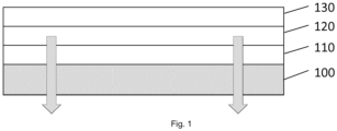
- Figure 1 represents simplified cross-section of bottom emission OLED device.
- the material film (110) is applied on the TFT Substrate (100) which may or may not contain also color filter (color filter on array, COA design) followed by the deposition of the OLED layers (120).
- the device may be finalized by deposition of the device encapsulation layers (130).
- the refractive index and film thickness requirements of the material coating layer (110) are defined by the optics of the TFT Substrate (100) and OLED layer (120) design to maximize the out-coupling of the light emitted from the OLED device layer pixels travelling through the TFT Substrate for improved device efficiency.
- the cathode of the OLED layer is non-transparent thus reflecting the emitted light downwards (see direction of arrows in Figure 1 ).
- the material coating layer (110) can be used also for tuning of the possible micro-cavity effects to improve device efficiency.
- OLED device can be also a lighting panel, in which case the driver circuitry can be a lot simpler, and in this case, it may be that the inventive material layer is deposited directly on device substrate (e.g. glass or plastic substrate) rather than on a thin film transistor structure.
- the inventive thin film again functions as out-coupling enhancement layer (improving external efficiency of the device), but at the same time can serve as a scatter layer, which might be a design requirement in case of lighting panel application.
- the material coating layer is used in connection to the substrate and scatter particles are introduced into the thin film coating formulation.
- Such particles usually provide additional optical effects, e.g. to meet specific requirements, such as for lighting applications.
- These particles can be, for example SiO 2 , TiO 2 , ZrO 2 , or similar inorganic particles.
- the inventive thin film acts as an optical layer but may also act as encapsulating layer.
- the thin-film can be used as an inorganic thin-film encapsulation layer as part of the full thin film encapsulation stack. Usually the encapsulation is accomplished using 3 to 10 layers.
- the inventive thin film can also act as planarization layer on top of the OLED (to help subsequent thin film encapsulation (TFE) layer deposition) and also allows tuning of the possible micro-cavity effect to improve efficiency of the device.
- the planarization layer can help to reduce particle defects, which typically can arise from vacuum vapor deposition of the specific thick inorganic TFE layer.
- the inventive thin film layer is particulate free, it will not inherently generate any particle defect to the thin film stack, which is potentially a big issue with the incumbent technologies where you mix nano/micro particles in polymer matrices and you will always have some particle agglomerates, which will be source for defect in the device and degradation of its lifetime. Also breaking the thin film encapsulation layer to thinner max 2-4um thick individual layers it will help to retain the flexibility of the structure, allowing flexibility of the device structure.
- FIG. 2 represents a simplified cross-section of a top emission OLED device.
- OLED Layers (210) e.g. Anode/Hole transport layer/Emissive layer/Electron transport layer/Cathode
- Material coating layer or layers (220) are deposited on the OLED layers (210).
- material coating layer (220) optional capping layer, can be inventive HRI material
- the device encapsulation layers (230) (240) (250) are deposited.
- layers 230 and 250 would be very thin inorganic layers such as silicon nitride and 240 would be the inventive HRI material sometimes referred to as particle covering layer (PCL).
- PCL particle covering layer
- the material coating layer(s) can be part of the encapsulation layer(s) or even in some arrangements it may be preferred the material coating layer can be preferred to be deposited as the last layer after the encapsulation layer(s) (various constructions comprising (230) and (240) can be envisioned.
- the OLED device is a top emission configuration where the light is emitted through the encapsulation layer(s) (see direction of the arrows in Figure 2 ).
- FIG. 3 Another potential configuration linked with the OLED is drawn in Figure 3 .
- the OLED Layers (310) e.g. Anode/Hole transport layer/Emissive layer/Electron transport layer/Cathode
- Material coating layer or layers (320) are deposited on the OLED layers (310).
- the device encapsulation layers (330) (340) (350) are deposited.
- layers 330 and 350 would be very thin inorganic layers such as silicon nitride and (340) would be the inventive HRI material sometimes referred to as particle covering layer (PCL).
- PCL particle covering layer
- the material coating layer(s) can be part of the encapsulation layer(s) or even in some arrangements it may be preferred the material coating layer can be preferred to be deposited as the last layer after the encapsulation layer(s) (various constructions comprising (330) and (340) can be envisioned. And the inorganic (330) and material coating layer (340) could be applied multiple times in order to reach the optimal result for the water/oxygen inhibition or optical effect.
- the OLED device is a top emission configuration where the light is emitted through the encapsulation layer(s) (see direction of the arrows in Figure 3 ).
- the top emission OLED structure it is preferable to be able to process the optical and FTE layers by using ink-jet printing or combined slit coating and ink-jet printing approach. This will allow eventually lower capital investment and lower cost production.
- Preferred variants and embodiments of the process of the present invention and the multi-layer structure of the present invention are also preferred variants and embodiments of the article according to the present invention.
- the present invention is furthermore directed to a composition comprising a first precursor composition (FPC) and a second precursor composition (SPC), the first precursor composition (FPC) being one or more polymerized metal or metalloid compound according to formula (I) M 1 (OR 1 ) n R 2 m (I) wherein
- Preferred features of the process according to the present invention are also preferred features of the composition of the present invention.
- the present invention is furthermore directed to a kit-of-parts comprising a first precursor composition (FPC) in a first vessel and a second precursor composition (SPC) in a second vessel, the first precursor composition (FPC) being one or more polymerized metal or metalloid compound according to formula (I) M 1 (OR 1 ) n R 2 m (I) wherein
- the present invention is furthermore directed to the use of the composition or the kit-of-parts according to the present invention for preparing a thin film on a substrate.
- the present invention is furthermore directed to the use of the composition or the kit-of-parts according to the present invention for preparing an optical or electrical coating.
- the present invention is furthermore directed to the use of the composition according to the present invention for preparing
- Figure 1 shows a simplified cross-section of bottom emission OLED device
- Figure 2 shows a simplified cross-section of a top emission OLED device
- Figure 3 shows a simplified cross-section of a top emission OLED device with thin film encapsulation layers
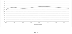
- Figure 4 shows the transmission graph of the film obtained in application example 19, (spectrum includes glass substrate).
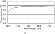
- Figure 5 shows the transmission graph of the film obtained in application example 24, (glass substrate subtracted).
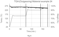
- FIG. 6 shows the weight loss, determined by Thermogravimetric analysis (TGA) of application example 24
- the tool used the measure molecular weight is WATERS GPC (gel permeation chromatography): waters 1515 Isocratic HPLC pump, waters 2414 refractive index detector. Polystyrene standards are used as calibration standards for the measurement. The actual samples for the measurements are prepared as 4m-% samples using THF as eluent solution.
- the tool used to determine the molecular weight is Mettler Toledo HB43 Halogen dryer/balance. Sample is weighted on aluminum dish/cup and measurement is performed using about 1 gram of material.
- Material shelf life is determined by following material process/application result stability/repeatability as cured film.
- the values monitored from cured film are film thickness and film refractive index.
- the film thickness and refractive index are characterized by using Ellipsometer (UVISEL-VASE Horiba Jobin-Yvon).
- Measurements are performed using Gorilla Glass 4 or silicon wafer (Diameter: 150 mm, Type/Dopant: P/Bor, Orientation: ⁇ 1-0-0>, Resistivity: 1-30 ohm ⁇ cm, Thickness: 675+/-25 ⁇ m, TTV: ⁇ 5 ⁇ m, Particle: ⁇ 20 @ 0.2 ⁇ m, Front Surface: Polished, Back Surface: Etched, Flat:1 SEMI Standard) as substrates.
- Material film depositions are done by using spin coating, pre-cured using hot-plate, UV-exposure performed by broadband UV source and final bake performed in convection oven. Optionally materials can be UV-cured only or thermal cured only.
- L*(D65), a*(D65) and b*(D65) and Haze were determined by using Konica Minolta spectrophotometer CM-3700A (SpectraMagic NX software). Measurements are performed using Gorilla Glass 4 as substrates. Material film depositions are done by using spin coating, pre-cured using hot-plate, UV-exposure performed by broadband UV source and final bake performed in convection oven. Optionally materials can be UV-cured only or thermal cured only. Also optionally the materials are ink-jet deposited on glass.
- the film refractive index is characterized by using Ellipsometer (UVISEL-VASE Horiba Jobin-Yvon). Measurements are performed using Gorilla Glass 4 or silicon wafer (Diameter: 150 mm, Type/Dopant: P/Bor, Orientation: ⁇ 1-0-0>, Resistivity: 1-30 ohm ⁇ cm, Thickness: 675+/-25 ⁇ m, TTV: ⁇ 5 ⁇ m, Particle: ⁇ 20 @ 0.2 ⁇ m, Front Surface: Polished, Back Surface: Etched, Flat:1 SEMI Standard) as substrates. Material film depositions are done by using spin coating, pre-cured using hot-plate, UV-exposure performed by broadband UV source and final bake performed in convection oven. Optionally materials can be UV-cured only or thermal cured only. Also optionally the materials are ink-jet deposited on glass.
- the film thickness is measured by using Ellipsometer (UVISEL-VASE Horiba Jobin-Yvon). Measurements are performed using Gorilla Glass 4 or silicon wafer (Diameter: 150 mm, Type/Dopant: P/Bor, Orientation: ⁇ 1-0-0>, Resistivity: 1-30 ohm ⁇ cm, Thickness: 675+/-25 ⁇ m, TTV: ⁇ 5 ⁇ m, Particle: ⁇ 20 @ 0.2 ⁇ m, Front Surface: Polished, Back Surface: Etched, Flat:1 SEMI Standard) as substrates. Material film depositions are done by using spin coating, pre-cured using hot-plate, UV-exposure performed by broadband UV source and final bake performed in convection oven. Optionally materials can be UV-cured only or thermal cured only. Also optionally the materials are ink-jet deposited on glass.
- a sample of 2.0 mg weight was set in TGA/DTA Simultaneous Measuring Instrument DTG-60A, Shimadzu Japan, and heated up to 160°C, 230°C and 250°C continuously under Nitrogen flow atmosphere.
- the heating rate was 10°C/min and the temperature of 160°C was held for 60 min, the temperature of 230°C was held for 60 min and the temperature of 250°C was held for 30 min.
- inventive example 1 was repeated except that 8.4 g of tetraisopropylorthotitanate was used, resulting in a transparent solution with an SC of 15 wt.%.
- inventive example 2 was repeated except that instead of trimethylamine, 0.2 g of 2,6,10-trimethyl-2,6,10-triazaundecane was used, resulting in a transparent solution with an SC of 15 wt.%.
- inventive example 1 was repeated except that 5.2 g of 3-glycidoxypropylmethyldimethoxysilane instead of methacryloxypropylmethyldimethoxysilane was used, resulting in a transparent solution with an SC of 14 wt.%.
- inventive example 4 was repeated except that 11 g of 3-glycidoxypropylmethyldimethoxysilane was used, resulting in a transparent solution with an SC of 20 wt.%.
- inventive example 1 was repeated except that 2.34 g of mercaptpropyl methyldimethoxysilane was used instead of methacryloxypropylmethyldimethoxysilane, resulting in a transparent solution with an SC of 17 wt.%.
- inventive example 9 was repeated except that 8.4 g tetraisopropylorthotitanate was used, resulting in a transparent solution with an SC of 16 wt.%.
- inventive example 5 The procedure of inventive example 5 was repeated whereby to 30 g of the resulting transparent solution 6 g of ethylacetoacetate was added and the resulting mixture was stirred for 24 h at 25°C, resulting in a transparent solution with an SC of 17 wt.%.
- inventive example 5 The procedure of inventive example 5 was repeated whereby to 30 g of the resulting transparent solution 12 g of ethylacetoacetate was added and the resulting mixture was stirred for 48 h at 25°C, resulting in a transparent solution with an SC of 13 wt.%.
- inventive example 11 was repeated whereby to 20 g of the resulting transparent solution 4 g of ethylacetoacetate and 16 g propyleneglycolmonomethylether were added and the resulting mixture was stirred for 72 h at 25°C, resulting in a transparent solution with an SC of 10 wt.%.
- Solution 1 Methacryloxypropyltriethoxysilane (120g) was added to the reaction flask and 21g water (0.1M HNO 3 ) was added. The reaction mixture was refluxed at 95°C in an oil bath for 3 hours and 40 min. The solution was cooled down and mixture of triethylamine (0.39 g) and 2-propanol (3.51 g) was added and refluxing was continued for 65 min. After reflux, solvent was removed under reduced vacuum. Molecular weight of the material was 1000.
- Solution 2 Methacryloxypropyltriethoxysilane (36g) was added to the reaction flask and 6.3g water (0.1M HNO 3 ) was added. The reaction mixture was stirred at room temperature for 3 days. Solvent removal was done under reduced pressure. Molecular weight of the material was 1000. Mixture preparation: To the 500 ml round bottom flask was added solution 1 (77 g), solution 2 (3g) and Miramer M1142 (20 g). Solution was mixed at room temperature for 2 hours.
- Solution 2 Methacryloxypropyltriethoxysilane (36g) was added to the reaction flask and 6.3g water (0.1M HNO 3 ) was added. The reaction mixture was stirred at room temperature for 3 days. Solvent removal was done under reduced pressure. Molecular weight of the material was 1000. Mixture preparation: To the 500 ml round bottom flask was added solution 1 (77 g), solution 2 (3 g) and Miramer M1142 (20 g). Solution was mixed at room temperature for 2 hours.
- Solution 1 To the Zirkonium (IV) isopropoxide solution 70 % in 2-propanol (50 g) was added Ethylacetoacetate (83.43 g). Solution was mixed at room temperature for 5 days. Solvent removal was done under reduced pressure. Mass of the solution after solvent removal was 96.2 g.
- Solution 2 Methacryloxypropyltriethoxysilane (36 g) was added to the reaction flask and 6.3 g water (0.1M HNO 3 ) was added. The reaction mixture was stirred at room temperature for 3 days. Solvent removed was done under reduced pressure. Molecular weight of the material was 1000.
- Mixture preparation To the 100 ml flask was added solution 1 (67 g), solution 2 (3 g), Miramer M244 (30 g) and BYK3700 (2 g). Solution was mixed 2 hours at room temperature.
- Solution 2 Methacryloxypropyltriethoxysilane (36 g) was added to the reaction flask and 6.3 g water (0.1 M HNO 3 ) was added. The reaction mixture was stirred at room temperature for 3 days. Solvent removed was done under reduced pressure. Molecular weight of the material was 1000. Mixture preparation: To the 100 ml flask was added solution 1 (67 g), solution 2 (3 g), Miramer M1142 (30 g) and BYK3700 (2 g). Solution was mixed 2 hours at room temperature.
- Solution 2 Miramer 1142 (90 g) was added to the reaction flask, 2-propanol (60g) and 5.1 g water (0.01M HNO 3 ) was added. Solution was stirred at room temperature for 16 hours.
- Solution 2 Miramer 1142 (90 g) was added to the reaction flask, 2-propanol (60 g) and 5.1 g water (0.01 M HNO 3 ) was added. Solution was stirred at room temperature for 16 hours. Solution 3. Phenyltrimethoxysilane (5.42 g) was added to the round bottom flask and 1.42 g of water (0.01 M HNO 3 ) was added. Solution was stirred at room temperature for 16 hours.
- Solution 2 (9.36 g) and Solution 1 (144.0 g) were combined. To the combined solution was added 2-methoxy-1-propanol (252.0 g). Solution 3 (0.41 g) was added to the Solution 1+2. At the end 361.38 g of 2-methoxy-1-propanol was added. Solution was stirred at room temperature over a night.
- Solution 1 To the Zirkonium (IV) butoxide solution 80 % in butanol (1963 g), was added Ethylacetoacetate (1066 g). Solution was mixed at room temperature for 5 days. Solvent removal was done under reduced pressure.
- Solution 2 Miramer 1142 (90 g) was added to the reaction flask, 2-propanol (60g) and 5.1g water (0.01 M HNO 3 ) was added. Solution was stirred at room temperature for 16 hours.
- Solution 3 Phenyltrimethoxysilane (5.42 g) was added to the round bottom flask and 1.42 g of water (0.01M HNO 3 ) was added. Solution was stirred at room temperature for 16 hours.
- solvent PGME various solvents can be used - from single solvents like THF-A (tetrahydrofurfuryl alcohol), PGMEA, Cyclohexanone, Ethylene glycol, Dipropylene glycol monomethyl ether, Diethylene glycol ethyl ether, and their combinations in different ratios.
- THF-A tetrahydrofurfuryl alcohol
- PGMEA tetrahydrofurfuryl alcohol
- Cyclohexanone Cyclohexanone
- Ethylene glycol Dipropylene glycol monomethyl ether
- Diethylene glycol ethyl ether Diethylene glycol ethyl ether
- Solution 1 To the Zirkonium (IV) butoxide solution 80 % in butanol (1963 g), was added Ethylacetoacetate (1066 g). Solution was mixed at room temperature for 5 days. Solvent removal was done under reduced pressure. Solution 2. Miramer 1142 (90g) was added to the reaction flask, 2-propanol (60g) and 5.1g water (0.01M HNO3) was added. Solution was stirred at room temperature for 16 hours. Solution 3: Phenyltrimethoxysilane (5.42 g) was added to the round bottom flask and 1.42 g of water (0.01M HNO3 ) was added. Solution was stirred at room temperature for 16 hours.
- Solution 1 (268g) and Solution 2 (17.42 g) were combined.
- PGME (2-methoxy-1-propanol, 220.43 g).
- Amount of 0.50 g of solution 3 was added, and final mixture was stirred at room temperature over a night. Measured viscosity 6.9 mPa-s.
- Solution 1 To the Zirkonium (IV) butoxide solution 80 % in butanol (1963 g), was added Ethylacetoacetate (1066 g). Solution was mixed at room temperature for 5 days. Solvent removal was done under reduced pressure. Solution 2. Miramer 1142 (90 g) was added to the reaction flask, 2-propanol (60g) and 5.1g water (0.01 M HNO 3 ) was added. Solution was stirred at room temperature for 16 hours. Solution 3: Phenyltrimethoxysilane (5.42 g) was added to the round bottom flask and 1.42 g of water (0.01 M HNO 3 ) was added. Solution was stirred at room temperature for 16 hours.
- Solution 1 (268g) and Solution 2 (17,42g) were combined.
- Solution 1 To the Zirkonium (IV) butoxide solution 80 % in butanol (1963 g), was added Ethylacetoacetate (1066 g). Solution was mixed at room temperature for 5 days. Solvent removal was done under reduced pressure. Solution 2. Miramer 1142 (90 g) was added to the reaction flask, 2-propanol (60g) and 5.1g water (0.01 M HNO 3 ) was added. Solution was stirred at room temperature for 16 hours. Solution 3: Phenyltrimethoxysilane (5.42 g) was added to the round bottom flask and 1.42 g of water (0.01 M HNO 3 ) was added. Solution was stirred at room temperature for 16 hours.
- Solution 1 (268 g) and Solution 2 (17.42 g) were combined.
- Amount of 0.40 g solution 3 was added, and final mixture was stirred at room temperature over a night. Measured viscosity of solution was 20.0 mPa-s.
- inventive example 30 was repeated except that 2.3 g of chlorotrimethylsilane was used, resulting in a transparent solution with an SC of 21 wt.%.
- a mixture of 6.3g of diethoxydimethylsilane, 0.5 g of water, 4g of propyleneglycol monomethylether and 0.2 g of triethylamine was added to the reaction mixture drop-wisely and heated at 100°C for 18 hours, resulting in a transparent solution with an SC of 17 wt.%.
- the thin film coating material of inventive example 19 was deposited on glass by spray coating method. Coating material solid content was about 9.8%.
- the spray coat parameters to deposit the layer on Gorilla glass 4 are following: Scan speed: 300 mm/s, Pitch: 50 mm, Gap: 50-100 mm, Flow rate: 3-10 ml/min, Atomization air pressure: 5 kg/cm 2 . After spray deposition the films were cured in convection oven at 150C for 30 min. Figure 4 shows the transmission graph of the resulting material. The reflection and absorption of the glass substrate is not subtracted. Other optical properties of the film include: 92.3% transmission at 550 nm, a*(D65) 0.07 and b*(D65) 0.46. Refractive Index was 1.56 (at 632 nm) and final cured thickness 308 nm.
- inventive example 20 was tested by characterizing the material on silicon wafer (Diameter: 150 mm, Type/Dopant: P/Bor, Orientation: ⁇ 1-0-0>, Resistivity: 1-30 ohm ⁇ cm, Thickness: 675+/-25 ⁇ m, TTV: ⁇ 5 ⁇ m, Particle: ⁇ 20 @ 0.2 ⁇ m, Front Surface: Polished, Back Surface: Etched, Flat:1 SEMI Standard) and spin coating was used as deposition method in this case. Spin coating at 2000 rpm was used as deposition process, pre-bake at 100°C for 120 sec, Post-bake at 100°C for 30 min. Film thickness was measured to be 3.1 ⁇ m and Refractive index 1.608 (at 632 nm).
- inventive example 21 was tested by characterizing the material on silicon wafer (Diameter: 150 mm, Type/Dopant: P/Bor, Orientation: ⁇ 1-0-0>, Resistivity: 1-30 ohm ⁇ cm, Thickness: 675+/-25 ⁇ m, TTV: ⁇ 5 ⁇ m, Particle: ⁇ 20 @ 0.2 ⁇ m, Front Surface: Polished, Back Surface: Etched, Flat:1 SEMI Standard) and spin coating was used as deposition method in this case. Spin coating at 2000 rpm was used as deposition process, pre-bake at 100°C for 120 sec, Post-bake at 100°C for 30 min. Film thickness was measured to be 3.3 ⁇ m and Refractive index 1.613 (at 632 nm).
- inventive example 22 was tested by characterizing the material on silicon wafer (Diameter: 150 mm, Type/Dopant: P/Bor, Orientation: ⁇ 1-0-0>, Resistivity: 1-30 ohm ⁇ cm, Thickness: 675+/-25 ⁇ m, TTV: ⁇ 5 ⁇ m, Particle: ⁇ 20 @ 0.2 ⁇ m, Front Surface: Polished, Back Surface: Etched, Flat:1 SEMI Standard) and spin coating was used as deposition method in this case. Spin coating at 2000 rpm was used as deposition process, pre-bake at 100°C for 120 sec, Post-bake at 100°C for 30 min. Film thickness was measured to be 6.1 ⁇ m and Refractive index 1.585 (at 632nm).
- inventive example 23 was tested by characterizing the material on silicon wafer (Diameter: 150 mm, Type/Dopant: P/Bor, Orientation: ⁇ 1-0-0>, Resistivity: 1-30 ohm ⁇ cm, Thickness: 675+/-25 ⁇ m, TTV: ⁇ 5 ⁇ m, Particle: ⁇ 20 @ 0.2 ⁇ m, Front Surface: Polished, Back Surface: Etched, Flat:1 SEMI Standard) and spin coating was used as deposition method in this case. Spin coating at 2000 rpm was used as deposition process, pre-bake at 100°C for 120 sec, Post-bake at 100°C for 30 min. Film thickness was measured to be 6.1 ⁇ m and Refractive index 1.653 (at 632 nm).
- the thin film coating material of inventive example 24 was deposited on S2003F3, from Matsunami Glass Ind., Ltd. by spin coating at 360 rpm for 30 seconds with a spin-coater, 1H-DX2, from Mikasa Co., Ltd., Japan. Pre-bake 100°C 120 sec, Post-bake 250°C 30 min. Film thickness was measured to be 200 nm and Refractive index 1.71 (at 632 nm). Then 1-bromonaphthalene from Wako Pure Chemical Industries, Ltd., Japan was additionally applied on the surface of the coating at the thickness of 58 um to eliminate thin film interference effect for the transmittance measurement and covered with same slide glass plate.
- Figure 5 shows the transmission graph of the material.
- Other optical properties of the thin film include (substrate excluded): 99.1% transmission at 550 nm, a*(D65) -0.35 and b*(D65) 0.45.
- the thickness of the obtained films of application example 24 and application example 24C during the course of 23 weeks at +4°C and +23°C was determined.
- the differences in refractive index at +4°C and +23°C was also determined. The results are shown in the following tables.
- Thickness of the film of application example 24 [nm] 0 days 5 weeks 10 weeks 23 week +4°C 458 452 422 467 +23°C 458 424 440 451
- Refractive index of the film of application example 24 0 days 5 weeks 10 weeks 23 week +4°C 1.710 1.707 1.710 1.71 +23°C 1.710 1.709 1.707 1.70
- the data in the tables above represent shelf-life stability data for the material of inventive example 24. Ready to use formulation shelf-life has been analyzed at +4°C and +23°. Two different spin speed and resulting film thicknesses were analyzed in terms of film thickness consistency and refractive index consistency during the period of 23 weeks. From the data it can be confirmed that the material of inventive example 24 is very stabile at both ageing temperatures.
- the thin film coating material of inventive example 25 was deposited on Gorilla glass 4 by spin coating method.
- the material was characterized on glass substrate and spin coating was used as deposition method.
- Spin coating at 2000 rpm was used as deposition process, pre-bake 100°C 120 sec, Post-bake 250°C.
- Film thickness was measured to be 56 nm and Refractive index 1.72 (at 632 nm).
- the only difference between Example 24 and 25 material is the further dilution of the material in case of sample 25 to result in thinner film.
- the thin film coating material of inventive example 26 was tested by characterizing the material on Gorilla Glas 4 and spin coating was used as deposition method in this case. Spin coating at 2000 rpm was used as deposition process, pre-bake at 100°C for 120 sec, Post-bake at 250°C for 30 min.
- the thin film coating material of inventive example 28 was deposited on glass by ink-jet printing coating method.
- the material was characterized on Gorilla glass 4 and silicon wafers (Diameter: 150 mm, Type/Dopant: P/Bor, Orientation: ⁇ 1-0-0>, Resistivity: 1-30 ohm ⁇ cm, Thickness: 675+/- 25 ⁇ m, TTV: ⁇ 5 ⁇ m, Particle: ⁇ 20 @ 0.2 ⁇ m, Front Surface: Polished, Back Surface: Etched, Flat:1 SEMI Standard) and ink-jet coating was used as deposition method.
- Ink-jet printing (Dimatix Materials Printer DMP-2850; Jets 16, jetting frequency 5kHz, applied voltage 20V, drop spacing 30 ⁇ m, cartridge type 10pL) was used as deposition process, pre-bake at 100°C for 120 sec, Post-bake at 250°C for 30 minutes. Film thickness was measured to be 450 nm and Refractive index 1.71 (at 632 nm).
- the thin film coating material of inventive example 28 was further modified by introducing scatter particles (TiO 2 with an average particle size of 200 nm, obtainable from Kronos) in to the material at two different concentrations.
- Application example 28B was prepared by adding 3.8 weight-% of the scatter particles by weight to the inventive example 28 formulation and application example 28C was prepared by adding 4.8 weight-% of the scatter particles into the inventive example 28 formulation.
- the thin film coating material of inventive example 28B and 28C were deposited on Gorilla glass 4 by spin coating method. Spin coating at 400 rpm was used as deposition process, pre-bake at 100°C for 120 sec, Post-bake at 250°C for 30 minutes. Film thickness was measured to be 400 nm. Other optical data of the two application examples listed in the below table.
- Application example 28B Application example 28C thickness [nm] 400 400 Haze 15% 18% ⁇ a* 1.21 2.52 ⁇ b* (yellowing) -0.72 -0.47 L* 71.57 61.45 transmission (400 nm) [%] 50.59 36.10 transmission (550 nm) [%] 46.44 31.81
Landscapes
- Chemical & Material Sciences (AREA)
- Organic Chemistry (AREA)
- Chemical Kinetics & Catalysis (AREA)
- Materials Engineering (AREA)
- Life Sciences & Earth Sciences (AREA)
- Engineering & Computer Science (AREA)
- General Chemical & Material Sciences (AREA)
- Geochemistry & Mineralogy (AREA)
- Wood Science & Technology (AREA)
- Health & Medical Sciences (AREA)
- Medicinal Chemistry (AREA)
- Polymers & Plastics (AREA)
- Composite Materials (AREA)
- Inorganic Chemistry (AREA)
- Inorganic Compounds Of Heavy Metals (AREA)
- Laminated Bodies (AREA)
- Paints Or Removers (AREA)
- Application Of Or Painting With Fluid Materials (AREA)
- Oxygen, Ozone, And Oxides In General (AREA)
- Electroluminescent Light Sources (AREA)
- Silicon Compounds (AREA)
- Manufacture Of Macromolecular Shaped Articles (AREA)
Claims (15)
- Verfahren zum Herstellen einer Dünnschicht auf einem Substrat, das Verfahren die folgenden Schritte umfassend:a) Herstellen einer ersten Vorstufenzusammensetzung (FPC) in einem ersten Behälter, wobei die Herstellung die folgenden Schritte umfasst:a1) Bereitstellen mindestens einer Metall- oder Metalloidverbindung gemäß der folgenden Formel (I)
M1(OR1)nR2 m (I)
wobeiM1 ein Metall oder ein Metalloid, ausgewählt aus Si, Ti, Zr, Ge, Sb, mit einer Wertigkeit z ist,R1 jeweils unabhängig ausgewählt ist aus einer C1- bis C10-Organyl- oder Organoheteryl-Gruppe;R2 jeweils unabhängig ausgewählt ist aus einer C1- bis C20-Organyl- oder Organoheteryl-Gruppe;n 1 bis z ist,m z-1 bis 0 ist,n+m z ist,a2) mindestens teilweises Hydrolysieren der M1(OR1)-Reste und Polymerisieren der Metall- oder der Metalloidverbindung gemäß Formel (I),b) Herstellen einer zweiten Vorstufenzusammensetzung (SPC) in einem zweiten Behälter, wobei die Herstellung die folgenden Schritte umfasst:b1a) Bereitstellen einer Metall- oder Metalloidverbindung gemäß der folgenden Formel (II),
M2(OR3)o (II)
wobeiM2 ein Metall oder ein Metalloid, ausgewählt aus Si, Ge, Sb, Ti, Zr, Al, Sn, W, Se, Cr, Ag oder Ni, mit einer Wertigkeit y ist, wobei M1 und M2 auf verschiedenen Elementen des Periodensystems basieren;R3 jeweils unabhängig ausgewählt ist aus einer C1- bis C10-Organyl- oder Organoheteryl-Gruppe;o y istb2a) gegebenenfalls Umsetzen der Metall- oder Metalloidverbindung gemäß Formel (II) mit einem von (OR3) verschiedenen Ligand (L);
oderb1b) direktes Bereitstellen des Reaktionsprodukts aus Schritt b2a);c) Mischen der ersten Vorstufenzusammensetzung (FPC) mit der zweiten Vorstufenzusammensetzung (SPC);c1) gegebenenfalls Umsetzen des Produkts aus Schritt c) mit Si(R23)3X oder Si(R23)2X2, wobei R23 eine C1- bis C3-Alkyl-Gruppe ist,X CI oder OR24 repräsentiert,R24 eine C1- bis C3-Alkyl-Gruppe ist;d) Ausbilden einer Dünnschicht auf dem Substrat;e) gegebenenfalls teilweises oder vollständiges Entfernen des Lösemittels, wenn vorhanden, nach Schritt d) ;f) Härten des in Schritt e) erlangten Zwischenprodukts, wenn vorhanden, oder Schritt d), wenn Schritt e) nicht vorhanden ist,wobei gegebenenfalls ein (Meth)Acrylatester (ME) zugesetzt wird,- während der Herstellung der ersten Vorstufenzusammensetzung (FPC),- während der Herstellung der zweiten Vorstufenzusammensetzung (SPC) und/oder- während Schritt c) oder nach Schritt c), bevor Schritt d) durchgeführt wird. - Verfahren nach Anspruch 1, wobei in Schritt c) das Molverhältnis zwischen M1 und M2 von 1,0:10 bis 10:1,0, vorzugsweise von 1,0:10 bis 1,0:1,0, besonders bevorzugt von 1,0:10 bis 1,0:2,0 ist.
- Verfahren nach einem der vorhergehenden Ansprüche, wobei während Schritt c) Zusatzstoffe wie Tenside, Egalisiermittel, Verarbeitungshilfen, Antistatika, Antioxidantien, Wasser- und Sauerstofffänger, Katalysatoren, Streupartikel, Fotoinitiatoren oder Mischungen davon zugesetzt werden.
- Verfahren nach einem der vorhergehenden Ansprüche, wobei die maximale Temperatur während der Schritte d) bis f) unter 450 °C, vorzugsweise unter 300 °C liegt.
- Verfahren nach einem der vorhergehenden Ansprüche, wobei das Verfahren den folgenden Schritt c2) nach Schritt c) umfasst
c2) Zugeben eines Lösemittels (S) zu der in Schritt c) erlangten Mischung. - Verfahren nach einem der vorhergehenden Ansprüche, wobei der Feststoffgehalt vor Schritt d) nicht mehr als 75 Masse-%, vorzugsweise nicht mehr als 55 Masse-% ist.
- Verfahren nach einem der vorhergehenden Ansprüche 1 bis 4, wobei der Feststoffgehalt vor Schritt d) mindestens 90 Masse-% ist.
- Verfahren nach einem der vorhergehenden Ansprüche, wobei Schritt f) durch thermisches Härten und/oder Strahlungshärten bewirkt wird.
- Mehrschichtstruktur, mindestens eine Schicht umfassend, die aus der Dünnschicht besteht, die nach dem Verfahren nach einem der vorhergehenden Ansprüche hergestellt ist.
- Mehrschichtstruktur nach Anspruch 9, wobei eine Oberfläche der mindestens einen Schicht, die aus der Dünnschicht besteht, die nach dem Verfahren nach einem der Ansprüche 1 bis 10 hergestellt ist, in direktem Kontakt mit einer Oberfläche des Substrats und/oder mit einer anderen Schicht ist.
- Gegenstand, die Dünnschicht, die durch das Verfahren nach einem der Ansprüche 1 bis 8 erlangt werden kann, oder die Mehrschichtstruktur nach einem der Ansprüche 9 bis 10 umfassend.
- Gegenstand nach Anspruch 11, der ausgewählt ist aus- optischen und elektrischen Beschichtungen;- Dielektrika mit hohem k-Wert;- Lichtauskopplungs-/-extraktionsschichten;- Ätz- und CMP-Stoppschichten;- OLED-Schutz-/Versiegelungs-/Kapselungsbeschichtungen;- organischen Solarzellen; und- optischen Dünnschichtfiltern.
- Zusammensetzung, eine erste Vorstufenzusammensetzung (FPC) und eine zweite Vorstufenzusammensetzung (SPC) umfassend, wobei die erste Vorstufenzusammensetzung (FPC) mindestens eine polymerisierte Metall- oder Metalloidverbindung gemäß Formel (I) ist,
M1(OR1)nR2 m (I)
wobeiM1 ein Metall oder ein Metalloid, ausgewählt aus Si, Ti, Zr, Ge, Sb, mit einer Wertigkeit z ist,R1 jeweils unabhängig ausgewählt ist aus einer C1- bis C10-Organyl- oder Organoheteryl-Gruppe;R2 jeweils unabhängig ausgewählt ist aus einer C1- bis C20-Organyl- oder Organoheteryl-Gruppe;n 1 bis z-1 ist,m 1 bis z-1 ist,n+m z ist,wobei die Polymerisation durch mindestens teilweise Hydrolyse der M1(OR1)-Reste bewirkt wird;die zweite Vorstufenzusammensetzung (SPC) erlangt werden kann durchb1a) Bereitstellen einer Metall- oder Metalloidverbindung gemäß der folgenden Formel (II),
M2(OR3)o (II)
wobeiM2 ein Metall oder ein Metalloid, ausgewählt aus Si, Ge, Sb, Ti, Zr, Al, Sn, W, Se, Cr, Ag oder Ni, mit einer Wertigkeit y ist, wobei M1 und M2 auf verschiedenen Elementen des Periodensystems basieren;R3 jeweils unabhängig ausgewählt ist aus einer C1- bis C10-Organyl- oder Organoheteryl-Gruppe;o y ist,b2a) gegebenenfalls Umsetzen der Metall- oder Metalloidverbindung gemäß Formel (II) mit einem von (OR3) verschiedenen Ligand (L);
oderb1b) direktes Bereitstellen des Reaktionsprodukts aus Schritt b2a). - Kit, eine erste Vorstufenzusammensetzung (FPC) in einem ersten Behälter und eine zweite Vorstufenzusammensetzung (SPC) in einem zweiten Behälter umfassend, wobei die erste Vorstufenzusammensetzung (FPC) mindestens eine polymerisierte Metall- oder Metalloidverbindung gemäß Formel (I) ist,
M1(OR1)nR2 m (I)
wobeiM1 ein Metall oder ein Metalloid, ausgewählt aus Si, Ti, Zr, Ge, Sb, mit einer Wertigkeit z ist,R1 jeweils unabhängig ausgewählt ist aus einer C1- bis C10-Organyl- oder Organoheteryl-Gruppe;R2 jeweils unabhängig ausgewählt ist aus einer C1- bis C20-Organyl- oder Organoheteryl-Gruppe;n 1 bis z-1 ist,m 1 bis z-1 ist,n+m z ist,wobei die Polymerisation durch mindestens teilweise Hydrolyse der M1(OR1)-Reste bewirkt wird;die zweite Vorstufenzusammensetzung (SPC) erlangt werden kann durchb1a) Bereitstellen einer Metall- oder Metalloidverbindung gemäß der folgenden Formel (II),
M2(OR3)o (II)
wobeiM2 ein Metall oder ein Metalloid, ausgewählt aus Si, Ge, Sb, Ti, Zr, Al, Sn, W, Se, Cr, Ag oder Ni, mit einer Wertigkeit y ist, wobei M1 und M2 auf verschiedenen Elementen des Periodensystems basieren;R3 jeweils unabhängig ausgewählt ist aus einer C1- bis C10-Organyl- oder Organoheteryl-Gruppe;o y ist,b2a) gegebenenfalls Umsetzen der Metall- oder Metalloidverbindung gemäß Formel (II) mit einem von (OR3) verschiedenen Ligand (L);
oderb1b) direktes Bereitstellen des Reaktionsprodukts aus Schritt b2a). - Verwenden der Zusammensetzung nach Anspruch 13 oder des Kits nach Anspruch 14 zum Herstellen von einer Dünnschicht auf einem Substrat und/oder- optischen und elektrischen Beschichtungen;- Dielektrika mit hohem k-Wert;- Lichtauskopplungs-/-extraktionsschichten;- Ätz- und CMP-Stoppschichten;- OLED-Schutz-/Versiegelungs-/Kapselungsbeschichtungen;- organischen Solarzellen; und- optischen Dünnschichtfiltern.
Applications Claiming Priority (2)
| Application Number | Priority Date | Filing Date | Title |
|---|---|---|---|
| EP18158357 | 2018-02-23 | ||
| PCT/EP2019/054308 WO2019162374A1 (en) | 2018-02-23 | 2019-02-21 | Organomodified metal oxide or metalloid oxide polymer film |
Publications (2)
| Publication Number | Publication Date |
|---|---|
| EP3755672A1 EP3755672A1 (de) | 2020-12-30 |
| EP3755672B1 true EP3755672B1 (de) | 2024-08-07 |
Family
ID=61569036
Family Applications (1)
| Application Number | Title | Priority Date | Filing Date |
|---|---|---|---|
| EP19706616.0A Active EP3755672B1 (de) | 2018-02-23 | 2019-02-21 | Organomodifizierter metalloxid- oder metalloidoxid-polymerfilm |
Country Status (7)
| Country | Link |
|---|---|
| US (1) | US12240989B2 (de) |
| EP (1) | EP3755672B1 (de) |
| JP (1) | JP7416701B2 (de) |
| KR (1) | KR20200125934A (de) |
| CN (2) | CN119874207A (de) |
| TW (1) | TWI839346B (de) |
| WO (1) | WO2019162374A1 (de) |
Family Cites Families (23)
| Publication number | Priority date | Publication date | Assignee | Title |
|---|---|---|---|---|
| JPS59197401A (ja) | 1983-04-26 | 1984-11-09 | Nippon Oil & Fats Co Ltd | 光重合開始剤 |
| US4772530A (en) | 1986-05-06 | 1988-09-20 | The Mead Corporation | Photosensitive materials containing ionic dye compounds as initiators |
| IL84025A0 (en) * | 1986-10-03 | 1988-02-29 | Ppg Industries Inc | Organosiloxane/metal oxide coating compositions and their production |
| US4754012A (en) * | 1986-10-03 | 1988-06-28 | Ppg Industries, Inc. | Multi-component sol-gel protective coating composition |
| US4950581A (en) | 1987-07-06 | 1990-08-21 | Fuji Photo Film Co., Ltd. | Photopolymerizable composition |
| GB2304472B (en) | 1995-08-17 | 1999-03-24 | Deltron Components Ltd | Improvements in or relating to electrical terminals |
| AU717137B2 (en) | 1995-11-24 | 2000-03-16 | Ciba Specialty Chemicals Holding Inc. | Borate coinitiators for photopolymerization |
| TW466256B (en) | 1995-11-24 | 2001-12-01 | Ciba Sc Holding Ag | Borate photoinitiator compounds and compositions comprising the same |
| MY132867A (en) | 1995-11-24 | 2007-10-31 | Ciba Specialty Chemicals Holding Inc | Acid-stable borates for photopolymerization |
| JP2000119586A (ja) * | 1998-10-12 | 2000-04-25 | Nikon Corp | コーティング組成物及びこれが塗布された光学物品 |
| US6218494B1 (en) | 1998-11-18 | 2001-04-17 | Essilor International - Compagnie Generale D'optique | Abrasion-resistant coating composition process for making such coating composition and article coated therewith |
| CN101805282B (zh) | 2004-02-23 | 2012-07-04 | 三菱化学株式会社 | 肟酯化合物、光聚合性组合物和使用该组合物的滤色器 |
| US7094709B2 (en) | 2004-06-15 | 2006-08-22 | Braggone Oy | Method of synthesizing hybrid metal oxide materials and applications thereof |
| US10690847B2 (en) | 2005-06-15 | 2020-06-23 | Braggone Oy | Method of making a photonic crystal device and photonic crystal device |
| WO2007062963A1 (en) | 2005-12-01 | 2007-06-07 | Ciba Holding Inc. | Oxime ester photoinitiators |
| WO2007071797A1 (es) | 2005-12-19 | 2007-06-28 | Uralita Sistemas De Tuberias, S.A. | Sistema distribuido de transmisión bidireccional de ondas guiadas y/o radiadas |
| EP1963374B1 (de) | 2005-12-20 | 2010-02-17 | Basf Se | Oximester-photoinitiatoren |
| US20090292039A1 (en) | 2006-12-27 | 2009-11-26 | Adeka Corporation | Oxime ester compound and photopolymerization initiator containing the same |
| JP2010015025A (ja) | 2008-07-04 | 2010-01-21 | Adeka Corp | 特定の光重合開始剤を含有する感光性組成物 |
| JP5685803B2 (ja) | 2008-07-24 | 2015-03-18 | Jsr株式会社 | 感放射線性樹脂組成物および液晶表示素子用スペーサーとその製造法 |
| US20140147684A1 (en) | 2012-11-26 | 2014-05-29 | Korea Institute Of Science And Technology | Gas barrier film and method of preparing the same |
| EP3234032A1 (de) * | 2014-12-19 | 2017-10-25 | Basf Se | Kombination von uv-absorber und pigment zum schutz von substraten aus uv/vis-strahlung |
| CN112166034A (zh) * | 2018-05-31 | 2021-01-01 | 柯尼卡美能达株式会社 | 气体阻隔性基材、其制造方法、具备该气体阻隔性基材的电子器件 |
-
2019
- 2019-02-21 EP EP19706616.0A patent/EP3755672B1/de active Active
- 2019-02-21 WO PCT/EP2019/054308 patent/WO2019162374A1/en not_active Ceased
- 2019-02-21 CN CN202510075678.4A patent/CN119874207A/zh active Pending
- 2019-02-21 JP JP2020544460A patent/JP7416701B2/ja active Active
- 2019-02-21 US US16/971,877 patent/US12240989B2/en active Active
- 2019-02-21 CN CN201980014109.1A patent/CN111770905A/zh active Pending
- 2019-02-21 TW TW108105779A patent/TWI839346B/zh active
- 2019-02-21 KR KR1020207024101A patent/KR20200125934A/ko active Pending
Also Published As
| Publication number | Publication date |
|---|---|
| US20200392368A1 (en) | 2020-12-17 |
| JP7416701B2 (ja) | 2024-01-17 |
| US12240989B2 (en) | 2025-03-04 |
| JP2021514299A (ja) | 2021-06-10 |
| EP3755672A1 (de) | 2020-12-30 |
| CN111770905A (zh) | 2020-10-13 |
| TW201938656A (zh) | 2019-10-01 |
| TWI839346B (zh) | 2024-04-21 |
| CN119874207A (zh) | 2025-04-25 |
| KR20200125934A (ko) | 2020-11-05 |
| WO2019162374A1 (en) | 2019-08-29 |
Similar Documents
| Publication | Publication Date | Title |
|---|---|---|
| KR101839397B1 (ko) | 실란커플링제, 네거티브형 감광성 수지 조성물, 경화막, 및 터치 패널용 부재 | |
| TWI450932B (zh) | 矽氧烷樹脂組成物及使用它之觸控面板用保護膜 | |
| JP6319082B2 (ja) | 感光性樹脂組成物、それを熱硬化させてなる保護膜又は絶縁膜、それを用いたタッチパネル及びその製造方法 | |
| TWI528112B (zh) | 正型感光性矽氧烷組成物 | |
| TWI734763B (zh) | 低溫可硬化的負型感光性組成物、以及硬化膜之製造方法 | |
| EP1942150B1 (de) | Siloxanharzzusammensetzung und herstellungsverfahren dafür | |
| US8993214B2 (en) | Positive photosensitive siloxane composition | |
| CN112368611A (zh) | 树脂组合物、遮光膜、遮光膜的制造方法及带隔壁的基板 | |
| US20120178022A1 (en) | Positive photosensitive resin composition, cured film obtained using same, and optical device | |
| CN103995437B (zh) | 负型感光性硅氧烷组合物 | |
| KR20150118091A (ko) | 네거티브형 감광성 착색 조성물, 경화막, 터치패널용 차광 패턴 및 터치패널의 제조 방법 | |
| TWI720135B (zh) | 正型感光性矽氧烷組成物及其製造方法 | |
| US20190101828A1 (en) | Resin composition, cured film of same and method for manufacturing same, and solid-state image sensor | |
| JPWO2013157643A1 (ja) | ラジカル架橋性基を有するポリシロキサン組成物 | |
| EP3381969B1 (de) | Polymetalloxan, verfahren zur herstellung davon, zusammensetzung davon, gehärteter film und verfahren zur herstellung davon sowie elemente und elektronische bauteile damit | |
| JP2011173738A (ja) | 透明焼成体 | |
| JP7732206B2 (ja) | ネガ型感光性着色組成物、硬化膜、硬化膜の製造方法、隔壁付き基板、および画像表示装置 | |
| EP3755672B1 (de) | Organomodifizierter metalloxid- oder metalloidoxid-polymerfilm | |
| KR101998228B1 (ko) | 감광성 수지 조성물, 그로부터 형성된 경화막, 및 상기 경화막을 갖는 소자 | |
| TWI609927B (zh) | 含有機聚矽氧烷之可固化樹脂組成物 | |
| TWI512058B (zh) | 光硬化性塗佈組成物、光硬化塗佈膜及觸控面板 | |
| KR20100131915A (ko) | 감방사선성 조성물, 보호막 및 층간 절연막 및, 그들의 형성 방법 | |
| JP6711269B2 (ja) | 樹脂組成物、それを用いた固体撮像素子およびその製造方法 | |
| JP2023137277A (ja) | 感光性樹脂組成物および硬化膜 | |
| JP2024138960A (ja) | 改質金属酸化物粒子の製造方法、改質金属酸化物粒子、光硬化性組成物、硬化物 |
Legal Events
| Date | Code | Title | Description |
|---|---|---|---|
| STAA | Information on the status of an ep patent application or granted ep patent |
Free format text: STATUS: UNKNOWN |
|
| STAA | Information on the status of an ep patent application or granted ep patent |
Free format text: STATUS: THE INTERNATIONAL PUBLICATION HAS BEEN MADE |
|
| PUAI | Public reference made under article 153(3) epc to a published international application that has entered the european phase |
Free format text: ORIGINAL CODE: 0009012 |
|
| STAA | Information on the status of an ep patent application or granted ep patent |
Free format text: STATUS: REQUEST FOR EXAMINATION WAS MADE |
|
| 17P | Request for examination filed |
Effective date: 20200923 |
|
| AK | Designated contracting states |
Kind code of ref document: A1 Designated state(s): AL AT BE BG CH CY CZ DE DK EE ES FI FR GB GR HR HU IE IS IT LI LT LU LV MC MK MT NL NO PL PT RO RS SE SI SK SM TR |
|
| AX | Request for extension of the european patent |
Extension state: BA ME |
|
| DAV | Request for validation of the european patent (deleted) | ||
| DAX | Request for extension of the european patent (deleted) | ||
| GRAP | Despatch of communication of intention to grant a patent |
Free format text: ORIGINAL CODE: EPIDOSNIGR1 |
|
| STAA | Information on the status of an ep patent application or granted ep patent |
Free format text: STATUS: GRANT OF PATENT IS INTENDED |
|
| GRAJ | Information related to disapproval of communication of intention to grant by the applicant or resumption of examination proceedings by the epo deleted |
Free format text: ORIGINAL CODE: EPIDOSDIGR1 |
|
| INTG | Intention to grant announced |
Effective date: 20231019 |
|
| STAA | Information on the status of an ep patent application or granted ep patent |
Free format text: STATUS: REQUEST FOR EXAMINATION WAS MADE |
|
| INTC | Intention to grant announced (deleted) | ||
| GRAP | Despatch of communication of intention to grant a patent |
Free format text: ORIGINAL CODE: EPIDOSNIGR1 |
|
| STAA | Information on the status of an ep patent application or granted ep patent |
Free format text: STATUS: GRANT OF PATENT IS INTENDED |
|
| INTG | Intention to grant announced |
Effective date: 20240311 |
|
| GRAS | Grant fee paid |
Free format text: ORIGINAL CODE: EPIDOSNIGR3 |
|
| GRAA | (expected) grant |
Free format text: ORIGINAL CODE: 0009210 |
|
| STAA | Information on the status of an ep patent application or granted ep patent |
Free format text: STATUS: THE PATENT HAS BEEN GRANTED |
|
| AK | Designated contracting states |
Kind code of ref document: B1 Designated state(s): AL AT BE BG CH CY CZ DE DK EE ES FI FR GB GR HR HU IE IS IT LI LT LU LV MC MK MT NL NO PL PT RO RS SE SI SK SM TR |
|
| REG | Reference to a national code |
Ref country code: GB Ref legal event code: FG4D |
|
| REG | Reference to a national code |
Ref country code: CH Ref legal event code: EP |
|
| REG | Reference to a national code |
Ref country code: DE Ref legal event code: R096 Ref document number: 602019056511 Country of ref document: DE |
|
| REG | Reference to a national code |
Ref country code: IE Ref legal event code: FG4D |
|
| REG | Reference to a national code |
Ref country code: LT Ref legal event code: MG9D |
|
| REG | Reference to a national code |
Ref country code: NL Ref legal event code: MP Effective date: 20240807 |
|
| PG25 | Lapsed in a contracting state [announced via postgrant information from national office to epo] |
Ref country code: NO Free format text: LAPSE BECAUSE OF FAILURE TO SUBMIT A TRANSLATION OF THE DESCRIPTION OR TO PAY THE FEE WITHIN THE PRESCRIBED TIME-LIMIT Effective date: 20241107 |
|
| REG | Reference to a national code |
Ref country code: AT Ref legal event code: MK05 Ref document number: 1710781 Country of ref document: AT Kind code of ref document: T Effective date: 20240807 |
|
| PG25 | Lapsed in a contracting state [announced via postgrant information from national office to epo] |
Ref country code: NL Free format text: LAPSE BECAUSE OF FAILURE TO SUBMIT A TRANSLATION OF THE DESCRIPTION OR TO PAY THE FEE WITHIN THE PRESCRIBED TIME-LIMIT Effective date: 20240807 Ref country code: PT Free format text: LAPSE BECAUSE OF FAILURE TO SUBMIT A TRANSLATION OF THE DESCRIPTION OR TO PAY THE FEE WITHIN THE PRESCRIBED TIME-LIMIT Effective date: 20241209 Ref country code: GR Free format text: LAPSE BECAUSE OF FAILURE TO SUBMIT A TRANSLATION OF THE DESCRIPTION OR TO PAY THE FEE WITHIN THE PRESCRIBED TIME-LIMIT Effective date: 20241108 Ref country code: FI Free format text: LAPSE BECAUSE OF FAILURE TO SUBMIT A TRANSLATION OF THE DESCRIPTION OR TO PAY THE FEE WITHIN THE PRESCRIBED TIME-LIMIT Effective date: 20240807 Ref country code: PL Free format text: LAPSE BECAUSE OF FAILURE TO SUBMIT A TRANSLATION OF THE DESCRIPTION OR TO PAY THE FEE WITHIN THE PRESCRIBED TIME-LIMIT Effective date: 20240807 |
|
| PG25 | Lapsed in a contracting state [announced via postgrant information from national office to epo] |
Ref country code: BG Free format text: LAPSE BECAUSE OF FAILURE TO SUBMIT A TRANSLATION OF THE DESCRIPTION OR TO PAY THE FEE WITHIN THE PRESCRIBED TIME-LIMIT Effective date: 20240807 |
|
| PG25 | Lapsed in a contracting state [announced via postgrant information from national office to epo] |
Ref country code: LV Free format text: LAPSE BECAUSE OF FAILURE TO SUBMIT A TRANSLATION OF THE DESCRIPTION OR TO PAY THE FEE WITHIN THE PRESCRIBED TIME-LIMIT Effective date: 20240807 |
|
| PG25 | Lapsed in a contracting state [announced via postgrant information from national office to epo] |
Ref country code: AT Free format text: LAPSE BECAUSE OF FAILURE TO SUBMIT A TRANSLATION OF THE DESCRIPTION OR TO PAY THE FEE WITHIN THE PRESCRIBED TIME-LIMIT Effective date: 20240807 Ref country code: IS Free format text: LAPSE BECAUSE OF FAILURE TO SUBMIT A TRANSLATION OF THE DESCRIPTION OR TO PAY THE FEE WITHIN THE PRESCRIBED TIME-LIMIT Effective date: 20241207 |
|
| PG25 | Lapsed in a contracting state [announced via postgrant information from national office to epo] |
Ref country code: HR Free format text: LAPSE BECAUSE OF FAILURE TO SUBMIT A TRANSLATION OF THE DESCRIPTION OR TO PAY THE FEE WITHIN THE PRESCRIBED TIME-LIMIT Effective date: 20240807 |
|
| PG25 | Lapsed in a contracting state [announced via postgrant information from national office to epo] |
Ref country code: ES Free format text: LAPSE BECAUSE OF FAILURE TO SUBMIT A TRANSLATION OF THE DESCRIPTION OR TO PAY THE FEE WITHIN THE PRESCRIBED TIME-LIMIT Effective date: 20240807 Ref country code: RS Free format text: LAPSE BECAUSE OF FAILURE TO SUBMIT A TRANSLATION OF THE DESCRIPTION OR TO PAY THE FEE WITHIN THE PRESCRIBED TIME-LIMIT Effective date: 20241107 |
|
| PG25 | Lapsed in a contracting state [announced via postgrant information from national office to epo] |
Ref country code: RS Free format text: LAPSE BECAUSE OF FAILURE TO SUBMIT A TRANSLATION OF THE DESCRIPTION OR TO PAY THE FEE WITHIN THE PRESCRIBED TIME-LIMIT Effective date: 20241107 Ref country code: PT Free format text: LAPSE BECAUSE OF FAILURE TO SUBMIT A TRANSLATION OF THE DESCRIPTION OR TO PAY THE FEE WITHIN THE PRESCRIBED TIME-LIMIT Effective date: 20241209 Ref country code: PL Free format text: LAPSE BECAUSE OF FAILURE TO SUBMIT A TRANSLATION OF THE DESCRIPTION OR TO PAY THE FEE WITHIN THE PRESCRIBED TIME-LIMIT Effective date: 20240807 Ref country code: NO Free format text: LAPSE BECAUSE OF FAILURE TO SUBMIT A TRANSLATION OF THE DESCRIPTION OR TO PAY THE FEE WITHIN THE PRESCRIBED TIME-LIMIT Effective date: 20241107 Ref country code: NL Free format text: LAPSE BECAUSE OF FAILURE TO SUBMIT A TRANSLATION OF THE DESCRIPTION OR TO PAY THE FEE WITHIN THE PRESCRIBED TIME-LIMIT Effective date: 20240807 Ref country code: LV Free format text: LAPSE BECAUSE OF FAILURE TO SUBMIT A TRANSLATION OF THE DESCRIPTION OR TO PAY THE FEE WITHIN THE PRESCRIBED TIME-LIMIT Effective date: 20240807 Ref country code: IS Free format text: LAPSE BECAUSE OF FAILURE TO SUBMIT A TRANSLATION OF THE DESCRIPTION OR TO PAY THE FEE WITHIN THE PRESCRIBED TIME-LIMIT Effective date: 20241207 Ref country code: HR Free format text: LAPSE BECAUSE OF FAILURE TO SUBMIT A TRANSLATION OF THE DESCRIPTION OR TO PAY THE FEE WITHIN THE PRESCRIBED TIME-LIMIT Effective date: 20240807 Ref country code: GR Free format text: LAPSE BECAUSE OF FAILURE TO SUBMIT A TRANSLATION OF THE DESCRIPTION OR TO PAY THE FEE WITHIN THE PRESCRIBED TIME-LIMIT Effective date: 20241108 Ref country code: FI Free format text: LAPSE BECAUSE OF FAILURE TO SUBMIT A TRANSLATION OF THE DESCRIPTION OR TO PAY THE FEE WITHIN THE PRESCRIBED TIME-LIMIT Effective date: 20240807 Ref country code: ES Free format text: LAPSE BECAUSE OF FAILURE TO SUBMIT A TRANSLATION OF THE DESCRIPTION OR TO PAY THE FEE WITHIN THE PRESCRIBED TIME-LIMIT Effective date: 20240807 Ref country code: BG Free format text: LAPSE BECAUSE OF FAILURE TO SUBMIT A TRANSLATION OF THE DESCRIPTION OR TO PAY THE FEE WITHIN THE PRESCRIBED TIME-LIMIT Effective date: 20240807 Ref country code: AT Free format text: LAPSE BECAUSE OF FAILURE TO SUBMIT A TRANSLATION OF THE DESCRIPTION OR TO PAY THE FEE WITHIN THE PRESCRIBED TIME-LIMIT Effective date: 20240807 |
|
| PGFP | Annual fee paid to national office [announced via postgrant information from national office to epo] |
Ref country code: DE Payment date: 20250226 Year of fee payment: 7 |
|
| PG25 | Lapsed in a contracting state [announced via postgrant information from national office to epo] |
Ref country code: RO Free format text: LAPSE BECAUSE OF FAILURE TO SUBMIT A TRANSLATION OF THE DESCRIPTION OR TO PAY THE FEE WITHIN THE PRESCRIBED TIME-LIMIT Effective date: 20240807 Ref country code: DK Free format text: LAPSE BECAUSE OF FAILURE TO SUBMIT A TRANSLATION OF THE DESCRIPTION OR TO PAY THE FEE WITHIN THE PRESCRIBED TIME-LIMIT Effective date: 20240807 Ref country code: SM Free format text: LAPSE BECAUSE OF FAILURE TO SUBMIT A TRANSLATION OF THE DESCRIPTION OR TO PAY THE FEE WITHIN THE PRESCRIBED TIME-LIMIT Effective date: 20240807 |
|
| PG25 | Lapsed in a contracting state [announced via postgrant information from national office to epo] |
Ref country code: EE Free format text: LAPSE BECAUSE OF FAILURE TO SUBMIT A TRANSLATION OF THE DESCRIPTION OR TO PAY THE FEE WITHIN THE PRESCRIBED TIME-LIMIT Effective date: 20240807 |
|
| PG25 | Lapsed in a contracting state [announced via postgrant information from national office to epo] |
Ref country code: CZ Free format text: LAPSE BECAUSE OF FAILURE TO SUBMIT A TRANSLATION OF THE DESCRIPTION OR TO PAY THE FEE WITHIN THE PRESCRIBED TIME-LIMIT Effective date: 20240807 |
|
| PGFP | Annual fee paid to national office [announced via postgrant information from national office to epo] |
Ref country code: FR Payment date: 20250227 Year of fee payment: 7 |
|
| PG25 | Lapsed in a contracting state [announced via postgrant information from national office to epo] |
Ref country code: SK Free format text: LAPSE BECAUSE OF FAILURE TO SUBMIT A TRANSLATION OF THE DESCRIPTION OR TO PAY THE FEE WITHIN THE PRESCRIBED TIME-LIMIT Effective date: 20240807 |
|
| PGFP | Annual fee paid to national office [announced via postgrant information from national office to epo] |
Ref country code: GB Payment date: 20250324 Year of fee payment: 7 |
|
| REG | Reference to a national code |
Ref country code: DE Ref legal event code: R097 Ref document number: 602019056511 Country of ref document: DE |
|
| PLBE | No opposition filed within time limit |
Free format text: ORIGINAL CODE: 0009261 |
|
| STAA | Information on the status of an ep patent application or granted ep patent |
Free format text: STATUS: NO OPPOSITION FILED WITHIN TIME LIMIT |
|
| 26N | No opposition filed |
Effective date: 20250508 |
|
| PG25 | Lapsed in a contracting state [announced via postgrant information from national office to epo] |
Ref country code: SE Free format text: LAPSE BECAUSE OF FAILURE TO SUBMIT A TRANSLATION OF THE DESCRIPTION OR TO PAY THE FEE WITHIN THE PRESCRIBED TIME-LIMIT Effective date: 20240807 |
|
| PG25 | Lapsed in a contracting state [announced via postgrant information from national office to epo] |
Ref country code: MC Free format text: LAPSE BECAUSE OF FAILURE TO SUBMIT A TRANSLATION OF THE DESCRIPTION OR TO PAY THE FEE WITHIN THE PRESCRIBED TIME-LIMIT Effective date: 20240807 |
|
| REG | Reference to a national code |
Ref country code: CH Ref legal event code: PL |
|
| PG25 | Lapsed in a contracting state [announced via postgrant information from national office to epo] |
Ref country code: LU Free format text: LAPSE BECAUSE OF NON-PAYMENT OF DUE FEES Effective date: 20250221 |
|
| PG25 | Lapsed in a contracting state [announced via postgrant information from national office to epo] |
Ref country code: CH Free format text: LAPSE BECAUSE OF NON-PAYMENT OF DUE FEES Effective date: 20250228 |
|
| REG | Reference to a national code |
Ref country code: BE Ref legal event code: MM Effective date: 20250228 |