EP3719829A1 - Emitter, elektronenkanone, in der diese verwendet wird, elektronische vorrichtung, in der diese verwendet wird, und verfahren zu ihrer herstellung - Google Patents
Emitter, elektronenkanone, in der diese verwendet wird, elektronische vorrichtung, in der diese verwendet wird, und verfahren zu ihrer herstellung Download PDFInfo
- Publication number
- EP3719829A1 EP3719829A1 EP18883274.5A EP18883274A EP3719829A1 EP 3719829 A1 EP3719829 A1 EP 3719829A1 EP 18883274 A EP18883274 A EP 18883274A EP 3719829 A1 EP3719829 A1 EP 3719829A1
- Authority
- EP
- European Patent Office
- Prior art keywords
- nanowire
- emitter
- less
- single crystal
- electron gun
- Prior art date
- Legal status (The legal status is an assumption and is not a legal conclusion. Google has not performed a legal analysis and makes no representation as to the accuracy of the status listed.)
- Granted
Links
Images


Classifications
-
- H—ELECTRICITY
- H01—ELECTRIC ELEMENTS
- H01J—ELECTRIC DISCHARGE TUBES OR DISCHARGE LAMPS
- H01J1/00—Details of electrodes, of magnetic control means, of screens, or of the mounting or spacing thereof, common to two or more basic types of discharge tubes or lamps
- H01J1/02—Main electrodes
- H01J1/30—Cold cathodes, e.g. field-emissive cathode
- H01J1/304—Field-emissive cathodes
-
- C—CHEMISTRY; METALLURGY
- C01—INORGANIC CHEMISTRY
- C01B—NON-METALLIC ELEMENTS; COMPOUNDS THEREOF; METALLOIDS OR COMPOUNDS THEREOF NOT COVERED BY SUBCLASS C01C
- C01B32/00—Carbon; Compounds thereof
- C01B32/90—Carbides
- C01B32/914—Carbides of single elements
-
- H—ELECTRICITY
- H01—ELECTRIC ELEMENTS
- H01J—ELECTRIC DISCHARGE TUBES OR DISCHARGE LAMPS
- H01J37/00—Discharge tubes with provision for introducing objects or material to be exposed to the discharge, e.g. for the purpose of examination or processing thereof
- H01J37/02—Details
- H01J37/04—Arrangements of electrodes and associated parts for generating or controlling the discharge, e.g. electron-optical arrangement or ion-optical arrangement
- H01J37/06—Electron sources; Electron guns
- H01J37/073—Electron guns using field emission, photo emission, or secondary emission electron sources
-
- H—ELECTRICITY
- H01—ELECTRIC ELEMENTS
- H01J—ELECTRIC DISCHARGE TUBES OR DISCHARGE LAMPS
- H01J9/00—Apparatus or processes specially adapted for the manufacture, installation, removal, maintenance of electric discharge tubes, discharge lamps, or parts thereof; Recovery of material from discharge tubes or lamps
- H01J9/02—Manufacture of electrodes or electrode systems
- H01J9/022—Manufacture of electrodes or electrode systems of cold cathodes
- H01J9/025—Manufacture of electrodes or electrode systems of cold cathodes of field emission cathodes
-
- B—PERFORMING OPERATIONS; TRANSPORTING
- B82—NANOTECHNOLOGY
- B82Y—SPECIFIC USES OR APPLICATIONS OF NANOSTRUCTURES; MEASUREMENT OR ANALYSIS OF NANOSTRUCTURES; MANUFACTURE OR TREATMENT OF NANOSTRUCTURES
- B82Y30/00—Nanotechnology for materials or surface science, e.g. nanocomposites
-
- B—PERFORMING OPERATIONS; TRANSPORTING
- B82—NANOTECHNOLOGY
- B82Y—SPECIFIC USES OR APPLICATIONS OF NANOSTRUCTURES; MEASUREMENT OR ANALYSIS OF NANOSTRUCTURES; MANUFACTURE OR TREATMENT OF NANOSTRUCTURES
- B82Y40/00—Manufacture or treatment of nanostructures
-
- C—CHEMISTRY; METALLURGY
- C01—INORGANIC CHEMISTRY
- C01P—INDEXING SCHEME RELATING TO STRUCTURAL AND PHYSICAL ASPECTS OF SOLID INORGANIC COMPOUNDS
- C01P2004/00—Particle morphology
- C01P2004/10—Particle morphology extending in one dimension, e.g. needle-like
- C01P2004/16—Nanowires or nanorods, i.e. solid nanofibres with two nearly equal dimensions between 1-100 nanometer
-
- C—CHEMISTRY; METALLURGY
- C01—INORGANIC CHEMISTRY
- C01P—INDEXING SCHEME RELATING TO STRUCTURAL AND PHYSICAL ASPECTS OF SOLID INORGANIC COMPOUNDS
- C01P2004/00—Particle morphology
- C01P2004/80—Particles consisting of a mixture of two or more inorganic phases
-
- H—ELECTRICITY
- H01—ELECTRIC ELEMENTS
- H01J—ELECTRIC DISCHARGE TUBES OR DISCHARGE LAMPS
- H01J2201/00—Electrodes common to discharge tubes
- H01J2201/30—Cold cathodes
- H01J2201/304—Field emission cathodes
- H01J2201/30446—Field emission cathodes characterised by the emitter material
- H01J2201/30449—Metals and metal alloys
-
- H—ELECTRICITY
- H01—ELECTRIC ELEMENTS
- H01J—ELECTRIC DISCHARGE TUBES OR DISCHARGE LAMPS
- H01J2201/00—Electrodes common to discharge tubes
- H01J2201/30—Cold cathodes
- H01J2201/304—Field emission cathodes
- H01J2201/30446—Field emission cathodes characterised by the emitter material
- H01J2201/30484—Carbides
-
- H—ELECTRICITY
- H01—ELECTRIC ELEMENTS
- H01J—ELECTRIC DISCHARGE TUBES OR DISCHARGE LAMPS
- H01J2209/00—Apparatus and processes for manufacture of discharge tubes
- H01J2209/02—Manufacture of cathodes
- H01J2209/022—Cold cathodes
- H01J2209/0223—Field emission cathodes
-
- H—ELECTRICITY
- H01—ELECTRIC ELEMENTS
- H01J—ELECTRIC DISCHARGE TUBES OR DISCHARGE LAMPS
- H01J2237/00—Discharge tubes exposing object to beam, e.g. for analysis treatment, etching, imaging
- H01J2237/06—Sources
- H01J2237/063—Electron sources
- H01J2237/06308—Thermionic sources
- H01J2237/06316—Schottky emission
-
- H—ELECTRICITY
- H01—ELECTRIC ELEMENTS
- H01J—ELECTRIC DISCHARGE TUBES OR DISCHARGE LAMPS
- H01J2237/00—Discharge tubes exposing object to beam, e.g. for analysis treatment, etching, imaging
- H01J2237/06—Sources
- H01J2237/063—Electron sources
- H01J2237/06325—Cold-cathode sources
- H01J2237/06341—Field emission
Definitions
- the present invention relates to an emitter, an electron gun using the same, an electronic device using the same, and a method for manufacturing the same.
- an electron source using such an electron gun include a field emission-type electron source, a Schottky-type electron source, and the like. These are characterized in that the tip of an emitter used in an electron gun is sharpened to generate an electric field concentrating effect at the tip and to emit more electrons through the tip.
- PATENT LITERATURE 1 WO 2016/140177 A
- An object of the present invention is to provide an emitter made of hafnium carbide (HfC) single crystal wherein the emitter emits electrons in a stable and high efficiency, a method for manufacturing the emitter, and an electron gun and electronic device using the emitter.
- HfC hafnium carbide
- an emitter including a nanowire, the nanowire being made of hafnium carbide (HfC) single crystal, the longitudinal direction of the nanowire corresponding to the ⁇ 100> crystal direction of the hafnium carbide single crystal, the end of the nanowire through which electrons are to be emitted having the (200) plane and the ⁇ 311 ⁇ plane(s) of the hafnium carbide single crystal, the (200) plane is centered, and the ⁇ 311 ⁇ plane(s) surrounding the (200) plane, and also have found that the emitter has a field emission area more concentrated on the center (tip) of the emitter end than a conventional emitter made of hafnium carbide single crystal (specifically, a nanowire emitter made of hafnium carbide single crystal before being coated with hafnium oxide in Patent Literature 1), so that more stable electron emission can be provided as compared to a conventional emitter made
- HfC hafnium carbide
- the emitter equipped with a nanowire according to the present invention in which the nanowire is made of hafnium carbide (HfC) single crystal, the longitudinal direction of the nanowire corresponds to the ⁇ 100> crystal direction of the hafnium carbide single crystal, the end of the nanowire through which electrons are to be emitted has the (200) plane and the ⁇ 311 ⁇ plane(s) of the hafnium carbide single crystal, the (200) plane is centered, and the ⁇ 311 ⁇ plane(s) surrounds the (200) plane.
- HfC hafnium carbide
- the length in the lateral direction of the nanowire is 1 nm or more and 100 nm or less, and the length in the longitudinal direction of the nanowire may be 500 nm or more and 30 ⁇ m or less.
- the end through which electrons are to be emitted may have a tapered shape.
- the end through which electrons are to be emitted may be terminated with hafnium (Hf) of the hafnium carbide single crystal.
- the hafnium may be combined with oxygen and/or nitrogen.
- the end through which electrons are to be emitted may be coated with an oxide, nitride or oxynitride of the hafnium.
- the thickness of the hafnium oxide, nitride or oxynitride may be 1 nm or more and 5 nm or less.
- the emitter further includes a needle and a filament, in which the nanowire may be attached to the filament via the needle made of an element selected from the group consisting of tungsten (W), tantalum (Ta), platinum (Pt), rhenium (Re) and carbon (C).
- W tungsten
- Ta tantalum
- Pt platinum
- Re rhenium
- C carbon
- the electron gun may be a cold cathode field emission electron gun or a Schottky electron gun.
- An electronic device equipped with the electron gun according to the present invention has the above-mentioned electron gun as the electron gun, and the electronic device is selected from the group consisting of scanning electron microscope, transmission electron microscope, scanning transmission electron microscope, Auger electron spectrometer, electron energy loss spectrometer, and energy dispersive electron spectrometer, thereby solving the above problem.
- a method for manufacturing the above emitter according to the present invention includes a heating step of heating a nanowire made of hafnium carbide single crystal in vacuo, in which the longitudinal direction of the nanowire corresponds to the ⁇ 100> crystal direction of the hafnium carbide single crystal, the end of the nanowire is heated under a vacuum of 1 ⁇ 10 -10 Pa or more and 1 ⁇ 10 -6 Pa or less in a temperature range of 300°C or more and 1000°C or less for 5 seconds or more and 30 minutes or less, thereby solving the above problems.
- the end of the nanowire may be heated in a temperature range of more than 600°C and 1000°C or less for 1 minute or more and 5 minutes or less.
- the end of the nanowire may be heated in a temperature range of 650°C or more and 750°C or less for 1 minute or more and 5 minutes or less.
- the nanowire may be attached to a filament, and the filament is energized and heated.
- a step of introducing oxygen and/or nitrogen may be further included.
- oxygen and/or nitrogen may be introduced until the pressure becomes greater than 1 ⁇ 10 -6 Pa and 1 ⁇ 10 -4 Pa or less.
- the end of the nanowire may be heated in a temperature range of 650°C or more and 850°C or less for 3 minutes or more and 10 minutes or less.
- An emitter equipped with a nanowire made of hafnium carbide (HfC) single crystal according to the present invention is configured so that the longitudinal direction of the nanowire corresponds to the ⁇ 100> crystal direction of the hafnium carbide single crystal, the end of the nanowire through which electrons are to be emitted has the (200) plane and the ⁇ 311 ⁇ plane(s), the (200) plane is centered, and the ⁇ 311 ⁇ plane(s) surrounds the (200) plane.
- the field emission area can be more concentrated on the center (tip) of the emitter end than a conventional nanowire emitter made of hafnium carbide single crystal (specifically, a nanowire emitter made of hafnium carbide single crystal before being coated with hafnium oxide in Patent Literature 1).
- a conventional nanowire emitter made of hafnium carbide single crystal specifically, a nanowire emitter made of hafnium carbide single crystal before being coated with hafnium oxide in Patent Literature 1).
- electrons can be stably emitted with high efficiency.
- Using such an emitter can provide an electron gun which is stable for a long time, and an electronic device using it.
- the emitter equipped with a nanowire made of hafnium carbide (HfC) single crystal in addition that modifying the surface so that the end has the above-mentioned plane orientation can stably emit electrons with high efficiency, combining the end terminated with Hf with oxygen and/or nitrogen so as to coat its end with hafnium oxide, nitride or oxynitride can stably emit electrons with higher efficiency.
- HfC hafnium carbide
- the coated end to be coated is surface-modified so as to have the above-mentioned plane orientation, the coated end can stably emit electrons with higher efficiency, compared to the end of a conventional nanowire emitter made of hafnium carbide single crystal coated with hafnium oxide, nitride or oxynitride.
- a method for manufacturing a nanowire made of HfC single crystal according to the present invention includes a heating step of heating a nanowire made of HfC single crystal in vacuo under a predetermined condition, in which the longitudinal direction of the nanowire corresponds to the ⁇ 100> crystal direction of the HfC single crystal, and the end of the nanowire is heated under a vacuum of 1 ⁇ 10 -10 Pa or more and 1 ⁇ 10 -6 Pa or less in a temperature range of 300°C or more and 1000°C or less for 5 seconds or more and 30 minutes or less.
- the surface can be modified so that the end of the nanowire has the (200) plane and the ⁇ 311 ⁇ plane(s), the (200) plane is centered, and the ⁇ 311 ⁇ plane(s) surrounds the (200) plane.
- the above-mentioned "ordinary heat flashing" performed for cleaning a nanowire is an optional treatment in the method for manufacturing a nanowire made of HfC single crystal according to the present invention, because the surface modification can be performed so that the above end has the above-mentioned plane orientation, regardless of the presence or absence of the ordinary heat flashing.
- this treatment is preferable in that the end of the nanowire surface-modified to have the plane orientation is efficiently obtained.
- the present invention when the end of the nanowire made of HfC single crystal is heated under a predetermined condition in vacuo without performing an electrolytic evaporation treatment, an emitter can be obtained of which the above end is surface-modified so as to have the above-mentioned plane orientation. Therefore, in the present invention, the surface modification can be performed more easily than the case where the surface modification is performed by electrolytic evaporation treatment.
- Embodiment 1 describes an emitter according to the present invention and a method for manufacturing the same.
- FIG. 1 is a schematic view of the emitter according to Embodiment 1.
- the emitter according to the present invention includes a nanowire 100 made of hafnium carbide (hereinafter, referred to as HfC) single crystal 110. Furthermore, the longitudinal direction of the nanowire 100 corresponds to the ⁇ 100> crystal direction of the HfC single crystal. As shown in FIG. 1(B) , the end 120 of the nanowire 100 through which electrons are to be emitted has the (200) plane and the ⁇ 311 ⁇ plane(s) of the HfC single crystal 100, the (200) plane is centered, and the ⁇ 311 ⁇ plane(s) surrounds the (200) plane.
- HfC hafnium carbide
- the nanowire 100 is made of HfC single crystal 110, the end 120 through which electrons are to be emitted is controlled at an atomic level. Accordingly, electrons can be stably emitted. Furthermore, since the end 120 through which electrons are to be emitted is surface-modified to have the above-mentioned plane orientation, electrons can be stably emitted with high efficiency.
- a plane surrounding the (200) plane may have the ⁇ 201 ⁇ plane or the like in addition to the ⁇ 311 ⁇ plane(s). Also in this case, it is desirable that the plane is surface-modified so that the area of the ⁇ 311 ⁇ plane(s) is larger than that of the ⁇ 201 ⁇ plane.
- the length in the lateral direction (that is, the diameter) of the nanowire 100 is in a range of 1 nm or more and 100 nm or less, and the length in the longitudinal direction is in a range of 500 nm or more and 30 ⁇ m or less.
- an electric field concentration can be effectively generated at the end 120 through which electrons are to be emitted, so that more electrons can be emitted through the end.
- the length in the lateral direction of the nanowire 100 is in a range of 10 nm or more and 60 nm or less, and the length in the longitudinal direction is in a range of 5 ⁇ m or more and 30 ⁇ m or less.
- the nanowire 100 can be easily provided having the above-mentioned range and made of high-quality HfC single crystal with no cracks, kinks or the like.
- the end 120 through which electrons are to be emitted has a tapered shape.
- the ⁇ 311 ⁇ plane(s) can be configured to surround the (200) plane which is centered, as mentioned above.
- Such a processing and treatment can be performed using a heat treatment mentioned below.
- the end 120 of the emitter is surface-modified so as to have the above-mentioned plane orientation, as mentioned above, so that more tapered shape can be obtained than the case of a conventional nanowire emitter made of hafnium carbide single crystal (specifically, a nanowire emitter made of hafnium carbide single crystal before being coated with hafnium oxide in Patent Literature 1). Therefore, electrons are more efficiently emitted.
- a conventional nanowire emitter made of hafnium carbide single crystal specifically, a nanowire emitter made of hafnium carbide single crystal before being coated with hafnium oxide in Patent Literature 1). Therefore, electrons are more efficiently emitted.
- the end 120 through which electrons are to be emitted is terminated with Hf (hafnium) of the HfC single crystal.
- Hf hafnium
- the termination with Hf can be simply confirmed by calculating the work function.
- the Hf may be combined with oxygen and/or nitrogen. This reduces dangling bond and stabilizes the Hf, so that electrons can be emitted with high efficiency. More preferably, the combination of Hf with oxygen and/or nitrogen allows the end 120 through which electrons are to be emitted to be coated with hafnium oxide, nitride or oxynitride. When the end 120 has oxide, nitride or oxynitride, the material itself is stabilized, so that electrons can be emitted with high efficiency.
- the thickness of hafnium oxide, nitride or oxynitride is preferably in a range of 1 nm or more and 5 nm or less.
- the thickness is less than 1 nm, Hf might not be sufficiently stabilized.
- the thickness exceeds 5 nm, emission of electrons through the HfC single crystal 110 might be suppressed.
- the formation of hafnium oxide, nitride or oxynitride is estimated from experimental condition or by field emission measurement.
- the nanowire 100 is shown as the emitter itself, but is not limited thereto.
- the emitter may be the nanowire 100 itself, the nanowire 100 may be attached to and integrated with a needle, or may be further attached to a filament.
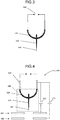
- FIG. 2 is a flowchart showing a method for manufacturing the emitter according to Embodiment 1.
- FIG. 3 is a schematic view showing a state in which a method for manufacturing the emitter according to Embodiment 1 is performed.
- Step 210 The nanowire 100 made of the hafnium carbide (HfC) single crystal 110 is heated in vacuo.
- the longitudinal direction of the nanowire 100 corresponds to the ⁇ 100> crystal direction of the HfC single crystal 110.
- the end of the nanowire 100 is heated in a heating condition under a vacuum of 1 ⁇ 10 -10 Pa or more and 1 ⁇ 10 -6 Pa or less in a temperature range of 300°C or more and 1000°C or less for 5 seconds or more and 30 minutes or less.
- the surface can be modified so that the end of the nanowire has the (200) plane and the ⁇ 311 ⁇ plane(s), the (200) plane is centered, and the ⁇ 311 ⁇ plane(s) surrounds the (200) plane.
- the "ordinary heat flashing" performed for cleaning a nanowire is an optional treatment, as mentioned above, and even without this treatment, the surface modification can be performed so that the above end has the above-mentioned plane orientation.
- the degree of vacuum exceeds 1 ⁇ 10 -6 Pa, the surface modification of the end of the HfC single crystal 110 may not sufficiently proceed.
- the lower limit of the degree of vacuum is not particularly limited, but the degree of vacuum is appropriately 1 ⁇ 10 -10 Pa in view of the limit of apparatus.
- the heating temperature is lower than 300°C, the surface modification of the end of the nanowire 100 may not sufficiently proceed.
- the heating temperature exceeds 1000°C, it becomes difficult to control the surface processing at an atomic level.
- the heating time is less than 5 seconds, the surface modification may not sufficiently proceed.
- the heating time exceeds 30 minutes, there is no change in the degree of surface modification, and thus such a condition is inefficient.
- heating is preferably performed in a temperature range of more than 600°C and 1000°C or less for 1 minute or more and 5 minutes or less.
- the end 120 of the nanowire 100 through which electrons are to be emitted has a tapered shape, and the HfC single crystal 110 is terminated with Hf.
- heating is performed in a temperature range of 650°C or more and 750°C or less for 1 minute or more and 5 minutes or less.
- the HfC single crystal 110 can be reliably terminated with Hf.
- the present inventors have experimentally confirmed the following: when the heating temperature is lower than 650°C, the end 120 may not be terminated with Hf, so that the work function may not be sufficiently reduced. Accordingly, from the viewpoint of more stably terminating the end 120 with Hf, the temperature is more preferably 650°C or more.
- a step of introducing oxygen and/or nitrogen may be performed.
- the end 120 through which electrons are to be emitted is terminated with Hf
- the end 120 can be made of Hf oxide, nitride or oxynitride.
- oxygen and/or nitrogen are introduced until the degree of vacuum is greater than 1 ⁇ 10 -6 Pa and 1 ⁇ 10 -4 Pa or less.
- hafnium oxide, nitride or oxynitride having a thickness in a range of 1 nm or more and 5 nm or less can be obtained.
- the end of the nanowire may be preferably heated in a temperature range of 650°C or more and 850°C or less for 3 minutes or more and 10 minutes or less. This promotes the growth of hafnium oxide, nitride or oxynitride.
- the method according to the present invention can be performed using a device shown in FIG. 3 .
- the nanowire 100 may be attached to a filament 320, and the filament 320 is energized and heated.
- the nanowire 100 is attached to the filament 320 via a needle 330 made of an element selected from the group consisting of tungsten (W), tantalum (Ta), platinum (Pt), rhenium (Re) and carbon (C).
- the nanowire 100 may be attached to a needle 330 through a conductive adhesive sheet such as a carbon pad.
- the device shown in FIG. 3 can be mounted on a vacuum chamber or the like to maintain a desired degree of vacuum.
- the heating temperature caused by the filament 320 can be measured by, for example, radiation thermometer or thermal imaging camera.
- Embodiment 2 describes an electron gun equipped with the emitter according to the present invention.
- FIG. 4 is a schematic view showing the electron gun according to Embodiment 2.
- the electron gun 400 includes at least the emitter 410 having the nanowire 100 described in Embodiment 1.
- the emitter 410 further includes, in addition to the nanowire 100, the filament 320 and the needle 330.
- the nanowire 100 is attached to the filament 320 via the needle 330 made of an element selected from the group consisting of tungsten (W), tantalum (Ta), platinum (Pt), rhenium (Re) and carbon (C). This is preferable because the handling of the nanowire 100 is simplified.
- the filament 320 has a hairpin-type shape (U-shape), but is not limited thereto.
- the filament 320 may have any shape such as a V-shape.
- an extraction power supply 450 is connected between an electrode 440 and an extraction electrode 460, in which the extraction power supply 450 applies a voltage between the emitter 410 and the extraction electrode 460.
- an acceleration power supply 470 is connected between the electrode 440 and an acceleration electrode 480, in which the acceleration power supply 470 applies a voltage between the emitter 410 and the acceleration electrode 480.
- the electrode 440 may be further connected to a flash power supply when the electron gun 400 is a cold cathode field emission electron gun, or may be connected to a heating power supply when the electron gun 400 is a Schottky electron gun.
- the electron gun 400 may be placed under a vacuum of 10 -8 Pa to 10 -7 Pa (10 -8 Pa or more and 10 -7 Pa or less). In this case, the end of the emitter 410 through which electrons are to be emitted can be kept clean.
- the electron gun 400 according to the present invention is a cold cathode field emission electron gun.
- the extraction power supply 450 applies a voltage between the emitter 410 and the extraction electrode 460. As a result, an electric field concentration is generated at the end of the nanowire 100 of the emitter 410 through which electrons are to be emitted, and thus electrons are extracted. Furthermore, the acceleration power supply 470 applies a voltage between the emitter 410 and the acceleration electrode 480. As a result, electrons extracted at the end of the nanowire 100 of the emitter 410 through which electrons are to be emitted are accelerated and emitted toward a sample.
- the surface of the nanowire 100 may be cleaned by, if needed, performing flashing using a flash power supply connected to the electrode 440. These operations are performed under the above-mentioned vacuum.
- thermoelectrons can be emitted from the nanowire 100 of the emitter 410 by the heating power supply, the electron gun 400 may further include a suppressor (not shown in the drawings) for shielding thermoelectrons.
- the electron gun 400 includes the emitter 410 equipped with the nanowire 100 described in detail in Embodiment 1, electrons can be easily and stably emitted for a long time.
- Such an electron gun 400 is employed in any electronic device having an electron focusing ability.
- such an electronic device is selected from the group consisting of scanning electron microscope, transmission electron microscope, scanning transmission electron microscope, Auger electron spectrometer, electron energy loss spectrometer and energy dispersive electron spectrometer.
- Example 1 an emitter was manufactured by modifying the surface of a nanowire made of HfC single crystal in a heating temperature range of 650°C to 750°C (650°C or more and 750°C or less).
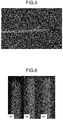
- Nanowires composed of HfC single crystal were manufactured by CVD method. Nanowires made of HfC single crystal were prepared on a graphite substrate in the same procedure and condition as in Reference Example 1 of Patent Literature 1. One of the nanowires was taken out and observed by scanning electron microscope (SEM, JSM-6500F, manufactured by JEOL) and transmission electron microscope (TEM, JEOL-2100F, manufactured by JEOL) equipped with an energy dispersive X-ray analyzer (EDS). The results are shown in FIG. 5 .
- FIG. 5 is a view showing a low magnification TEM image of a nanowire before undergoing surface modification.
- the synthesized nanowire is hafnium carbide (HfC).
- HfC hafnium carbide
- FIG. 5 it has been found that the nanowire is made of one type of crystal and has a length in the lateral direction of 60 nm and a length in the longitudinal direction of 3 ⁇ m.
- HRTEM image high-resolution transmission electron microscope image
- the longitudinal direction of the nanowire corresponds to the ⁇ 100> crystal direction of the HfC single crystal.
- SAED selected area electron diffraction pattern
- the nanowire was surface-modified to manufacture an emitter, using the device shown in FIG. 3 .
- the procedure for manufacturing the emitter was as follows. A wire made of tantalum was etched and processed into a Ta needle (330 in FIG. 3 ) having one end tapered. Next, the Ta needle was connected to a hairpin shaped tungsten filament (320 in FIG. 3 ) by welding. The nanowire (100 in FIG. 3 ) was fixed to the tapered Ta needle using a carbon pad. The degree of vacuum in a vacuum chamber was 1 ⁇ 10 -7 Pa.
- the nanowire was heated in vacuo (the step S210 in FIG. 2 ).
- a current of 2.3 A was applied to the tungsten filament via a power supply (340 in FIG. 3 ), and its state was maintained for 3 minutes.
- the temperature of the tungsten filament was measured by radiation thermometer, the temperature was 650°C to 750°C (650°C or more and 750°C or less).
- the nanowire thus obtained was observed by SEM. The results are shown in FIG. 6 .
- the time dependence of the field emission current of the emitter at room temperature and an extraction voltage of 720 V was measured using a field ion microscope (FIM). The results are shown in FIG. 7 .
- the field emission pattern was observed by inverting the polarity of the extraction voltage of the emitter to generate field emission. The results are shown in FIG. 10 .
- Example 2 an emitter was manufactured by surface-modifying a nanowire made of HfC single crystal that was manufactured by CVD method in the same manner as in Example 1 in a heating temperature range of 500°C to 600°C (500°C or more and 600°C or less).
- the condition for heating the nanowire was the same as that in Example 1, except that a current of 2.1 A (500°C to 600°C (500°C or more and 600°C or less) according to a radiation thermometer) was applied and its state was maintained for 1 minute.
- the nanowire thus obtained was observed by SEM. The results are shown in FIG. 6 .
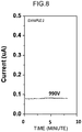
- the time dependence of the field emission current of the emitter at room temperature and an extraction voltage of 990 V was measured using an FIM.
- the results are shown in FIG. 8 .
- the field emission pattern was observed in the same manner as in Example 1.
- the results are shown in FIG. 10 .
- Example 2 In addition, in the same manner as in Example 1, the above-mentioned time dependence of the field emission current was measured while performing heating. At this time, the heating was at 1.5 A (in a range of 300°C or more and 500°C or less). The results are shown in FIG. 12 .
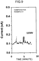
- Comparative Example 3 a nanowire made of HfC single crystal manufactured by CVD method in the same manner as in Example 1 was used for an emitter without surface modification by heating.
- the time dependence of the field emission current of the emitter at room temperature and an extraction voltage of 1330 V was measured using an FIM.
- the results are shown in FIG. 9 .
- the field emission pattern was observed in the same manner as in Example 1.
- the results are shown in FIG. 10 .
- Table 1 List of experimental condition for emitter according to Examples 1 and 2 / Comparative Example/ Comparative Example Size of HfC Heat-treatment condition Degree of vacuum (Pa) Temperature (°C) Current value (A) Time (minute) Example 1 3 ⁇ m in length, 60 nm ⁇ 1x10 -7 650 ⁇ 750 2.3 3 Example 2 3 ⁇ m in length, 60 nm ⁇ 1x10 -7 500 ⁇ 600 2.1 1 Comparative Example 3 3 ⁇ m in length, 60 nm ⁇ - - - - -
- FIG. 6 is an SEM image showing the ends of the nanowires according to Examples 1 and 2 / Comparative Example 3. The sizes are as described in "Size of HfC" in Table 1.
- FIGS. 6(A) to 6(C) are SEM images showing the ends of the nanowires according to Example 1, Example 2, and Comparative Example 3, respectively.
- the nanowire according to Comparative Example 3 shown in FIG. 6(C) is the same as that in FIG. 5 because it has not been heat-treated.
- FIG. 6(A) it has been found that the end of the nanowire according to Example 1 has a tapered shape and the surface has been modified.
- the end of the nanowire according to Example 2 shown in FIG. 6(B) is not as tapered as the end of the nanowire according to Example 1 shown in FIG. 6(A) , it indicates to have a slightly tapered shape, so that its surface has been modified. This indicates that heating the nanowire in vacuo is advantageous for surface modification.
- FIG. 7 is a diagram showing the time dependence of the field emission current of the emitter using a nanowire according to Example 1.
- FIG. 8 is a diagram showing the time dependence of the field emission current of the emitter using a nanowire according to Example 2.
- FIG. 9 is a diagram showing the time dependence of the field emission current of the emitter using a nanowire according to Comparative Example 3.
- the field emission current property of the nanowire according to Comparative Example 3 was not stable.
- the nanowire according to Example 1 exhibited relatively stable field emission current property over about 10 minutes, and the current value was as high as about 0.15 ⁇ A.
- the nanowire according to Example 2 exhibited more stable field emission current property than that of the nanowire according to Example 1, but the current value was smaller.
- FIG. 10 is a view showing the field emission patterns of nanowires according to Examples 1 and 2 / Comparative Example 3.
- FIGS. 10(A) to 10(C) show the field emission patterns of the nanowire according to Example 1, the nanowire according to Example 2, and the nanowire according to Comparative Example 3, respectively.
- areas shown bright in the gray scale are the field emission area.
- FIG. 10 it has been found that the field emission areas in the nanowires according to Examples 1 and 2 are wider and more concentrated at the center than the field emission areas in the nanowire according to Comparative Example 3. These results also indicate that the nanowires of which surfaces have been modified by heating in vacuo have improved field emission properties. Furthermore, comparing FIG. 10(A) with FIG. 10(B) , it has been found that the field emission area in the nanowire according to Example 1 is more concentrated at the center than that according to Example 2. Furthermore, when the plane index of the HfC single crystal in the field emission pattern was specified, it has been indicated that the ⁇ 311 ⁇ plane(s) surrounds the (200) plane with the (200) plane centered, as shown in FIG. 10(A) .
- the emitter of the present invention specifically, the emitter equipped with a nanowire made of hafnium carbide (HfC) single crystal, in which the longitudinal direction of the nanowire corresponds to the ⁇ 100> crystal direction of the hafnium carbide single crystal, and the end of the nanowire through which electrons are to be emitted has the (200) plane and the ⁇ 311 ⁇ plane(s), and the ⁇ 311 ⁇ plane(s) surrounds the (200) plane with the (200) centered), electrons can be emitted more efficiently and more stably, compared to conventional nanowire emitters made of hafnium carbide single crystal.
- HfC hafnium carbide
- FIG. 11 is a diagram showing the time dependence of the field emission current of the emitter using a nanowire according to Example 1 before or after undergoing heating.
- FIG. 12 is a diagram showing the time dependence of the field emission current of the emitter using a nanowire according to Example 2 before or after undergoing heating.
- the field emission current properties are further stabilized by heating, and in the nanowire according to Example 1, the current value is further improved. From this, it has been found that the properties of the nanowire according to the present invention are further improved by auxiliary heating current, and it is particularly advantageous for a Schottky electron gun among electron guns.
- Example 4 in the same manner as in Example 1, a nanowire made of surface-modified HfC single crystal was further treated with oxygen to manufacture an emitter.
- the conditions of the oxygen treatment are as follows: after performing the surface modification under the same condition as in Example 1, oxygen was introduced, the degree of vacuum after the oxygen introduction was maintained at 5 ⁇ 10 -5 Pa, a current of 2.5 A (800°C according to a radiation thermometer) was applied, and its state was maintained for 5 minutes.
- an oxide of Hf (HfOx : 0 ⁇ x ⁇ 2) was formed at the end of the HfC single crystal, and the thickness of the oxide was estimated to be 3 nm.
- the nanowire thus obtained was observed by SEM.
- the time dependence of the field emission current of the emitter at room temperature and an extraction voltage of 720 V was measured using an FIM, and the field emission pattern was observed.
- the field emission current properties of the nanowire according to Example 4 have improved current value. From this, it has been found that bonding the terminal Hf with oxygen, nitrogen or the like allows the nanowire according to the present invention to more efficiently and stably emit electrons because the end through which electrons are to be emitted is stabilized with the oxide, nitride or the like of Hf.
- the emitter according to the present invention allows electrons to be efficiently and stably emitted, it can be applied for any device having an electron focusing ability such as scanning electron microscope, transmission electron microscope, scanning transmission electron microscope, Auger electron spectrometer, electron energy loss spectrometer, and energy dispersive electron spectrometer.
Landscapes
- Chemical & Material Sciences (AREA)
- Organic Chemistry (AREA)
- Analytical Chemistry (AREA)
- Engineering & Computer Science (AREA)
- Manufacturing & Machinery (AREA)
- Inorganic Chemistry (AREA)
- Cold Cathode And The Manufacture (AREA)
- Electron Sources, Ion Sources (AREA)
Applications Claiming Priority (2)
| Application Number | Priority Date | Filing Date | Title |
|---|---|---|---|
| JP2017228505 | 2017-11-29 | ||
| PCT/JP2018/041601 WO2019107113A1 (ja) | 2017-11-29 | 2018-11-09 | エミッタ、それを用いた電子銃、それを用いた電子機器、および、その製造方法 |
Publications (3)
| Publication Number | Publication Date |
|---|---|
| EP3719829A1 true EP3719829A1 (de) | 2020-10-07 |
| EP3719829A4 EP3719829A4 (de) | 2021-08-11 |
| EP3719829B1 EP3719829B1 (de) | 2022-07-27 |
Family
ID=66665594
Family Applications (1)
| Application Number | Title | Priority Date | Filing Date |
|---|---|---|---|
| EP18883274.5A Active EP3719829B1 (de) | 2017-11-29 | 2018-11-09 | Emitter, elektronenkanone, in der diese verwendet wird, elektronische vorrichtung, in der diese verwendet wird, und verfahren zu ihrer herstellung |
Country Status (4)
| Country | Link |
|---|---|
| US (1) | US11417491B2 (de) |
| EP (1) | EP3719829B1 (de) |
| JP (1) | JP6804120B2 (de) |
| WO (1) | WO2019107113A1 (de) |
Cited By (1)
| Publication number | Priority date | Publication date | Assignee | Title |
|---|---|---|---|---|
| EP4050637A4 (de) * | 2019-10-21 | 2023-12-20 | National Institute for Materials Science | Emitter, elektronenkanone mit verwendung davon, elektronische vorrichtung mit verwendung davon und verfahren zur herstellung davon |
Families Citing this family (1)
| Publication number | Priority date | Publication date | Assignee | Title |
|---|---|---|---|---|
| JP7168269B2 (ja) | 2019-07-02 | 2022-11-09 | 国立研究開発法人物質・材料研究機構 | エミッタ、それを用いた電子銃、それを用いた電子機器、および、その製造方法 |
Family Cites Families (4)
| Publication number | Priority date | Publication date | Assignee | Title |
|---|---|---|---|---|
| US7828622B1 (en) | 2007-10-25 | 2010-11-09 | Kla-Tencor Technologies Corporation | Sharpening metal carbide emitters |
| US9240301B1 (en) | 2012-03-27 | 2016-01-19 | Applied Physics Technologies, Inc. | Thermal-field type electron source composed of transition metal carbide material with artificial facet |
| CN102629538B (zh) | 2012-04-13 | 2014-03-19 | 吴江炀晟阴极材料有限公司 | 具有低逸出功和高化学稳定性的电极材料 |
| WO2016140177A1 (ja) * | 2015-03-02 | 2016-09-09 | 国立研究開発法人物質・材料研究機構 | エミッタ、それを用いた電子銃、それを用いた電子機器、および、その製造方法 |
-
2018
- 2018-11-09 WO PCT/JP2018/041601 patent/WO2019107113A1/ja not_active Ceased
- 2018-11-09 US US16/767,689 patent/US11417491B2/en active Active
- 2018-11-09 EP EP18883274.5A patent/EP3719829B1/de active Active
- 2018-11-09 JP JP2019557110A patent/JP6804120B2/ja active Active
Cited By (1)
| Publication number | Priority date | Publication date | Assignee | Title |
|---|---|---|---|---|
| EP4050637A4 (de) * | 2019-10-21 | 2023-12-20 | National Institute for Materials Science | Emitter, elektronenkanone mit verwendung davon, elektronische vorrichtung mit verwendung davon und verfahren zur herstellung davon |
Also Published As
| Publication number | Publication date |
|---|---|
| WO2019107113A1 (ja) | 2019-06-06 |
| EP3719829B1 (de) | 2022-07-27 |
| US11417491B2 (en) | 2022-08-16 |
| EP3719829A4 (de) | 2021-08-11 |
| JP6804120B2 (ja) | 2020-12-23 |
| JPWO2019107113A1 (ja) | 2020-07-02 |
| US20200388458A1 (en) | 2020-12-10 |
Similar Documents
| Publication | Publication Date | Title |
|---|---|---|
| JP5794598B2 (ja) | 六ホウ化金属冷電界エミッター、その製造方法及び電子銃 | |
| EP4050637B1 (de) | Emitter, elektronenkanone mit verwendung davon, elektronische vorrichtung mit verwendung davon und verfahren zur herstellung davon | |
| JP6459135B2 (ja) | エミッタの製造方法 | |
| US8999178B2 (en) | Method for fabricating emitter | |
| EP3719829B1 (de) | Emitter, elektronenkanone, in der diese verwendet wird, elektronische vorrichtung, in der diese verwendet wird, und verfahren zu ihrer herstellung | |
| JP4292108B2 (ja) | 電子源及びその製造方法 | |
| US7828622B1 (en) | Sharpening metal carbide emitters | |
| JP5363413B2 (ja) | 電子源 | |
| CN101375363A (zh) | 金刚石电子发射阴极、电子源、电子显微镜及电子束曝光机 | |
| EP3920206B1 (de) | Emitter, elektronenkanone damit und elektronisches gerät | |
| JP4792404B2 (ja) | 電子源の製造方法 | |
| WO2007148507A1 (ja) | 電子源 | |
| EP3996126B1 (de) | Emitter, elektronenkanone mit dem emitter, elektronische vorrichtung mit der elektronenkanone, und verfahren zur herstellung des emitters | |
| JP2005032500A (ja) | 冷陰極とそれを用いた電子源及び電子線装置 | |
| JP4032057B2 (ja) | 電子源の製造方法 | |
| JP4867643B2 (ja) | ショットキーエミッタの製造方法 | |
| JPWO2004073010A1 (ja) | 電子銃 | |
| JP2005332677A (ja) | 電子源の製造方法と使用方法 | |
| JPH0612973A (ja) | 熱電界放射陰極の操作方法 | |
| JP2008098087A (ja) | 電子源 | |
| JP2009117134A (ja) | 電子線源の製造方法 |
Legal Events
| Date | Code | Title | Description |
|---|---|---|---|
| STAA | Information on the status of an ep patent application or granted ep patent |
Free format text: STATUS: THE INTERNATIONAL PUBLICATION HAS BEEN MADE |
|
| PUAI | Public reference made under article 153(3) epc to a published international application that has entered the european phase |
Free format text: ORIGINAL CODE: 0009012 |
|
| STAA | Information on the status of an ep patent application or granted ep patent |
Free format text: STATUS: REQUEST FOR EXAMINATION WAS MADE |
|
| 17P | Request for examination filed |
Effective date: 20200527 |
|
| AK | Designated contracting states |
Kind code of ref document: A1 Designated state(s): AL AT BE BG CH CY CZ DE DK EE ES FI FR GB GR HR HU IE IS IT LI LT LU LV MC MK MT NL NO PL PT RO RS SE SI SK SM TR |
|
| AX | Request for extension of the european patent |
Extension state: BA ME |
|
| DAV | Request for validation of the european patent (deleted) | ||
| DAX | Request for extension of the european patent (deleted) | ||
| A4 | Supplementary search report drawn up and despatched |
Effective date: 20210712 |
|
| RIC1 | Information provided on ipc code assigned before grant |
Ipc: H01J 1/304 20060101AFI20210706BHEP Ipc: B82Y 40/00 20110101ALI20210706BHEP Ipc: B82Y 99/00 20110101ALI20210706BHEP Ipc: H01J 9/02 20060101ALI20210706BHEP Ipc: H01J 37/073 20060101ALI20210706BHEP |
|
| RIC1 | Information provided on ipc code assigned before grant |
Ipc: B82Y 30/00 20110101ALI20220222BHEP Ipc: B82Y 40/00 20110101ALI20220222BHEP Ipc: B82Y 99/00 20110101ALI20220222BHEP Ipc: H01J 9/02 20060101ALI20220222BHEP Ipc: H01J 37/073 20060101ALI20220222BHEP Ipc: H01J 1/304 20060101AFI20220222BHEP |
|
| GRAP | Despatch of communication of intention to grant a patent |
Free format text: ORIGINAL CODE: EPIDOSNIGR1 |
|
| STAA | Information on the status of an ep patent application or granted ep patent |
Free format text: STATUS: GRANT OF PATENT IS INTENDED |
|
| INTG | Intention to grant announced |
Effective date: 20220412 |
|
| GRAS | Grant fee paid |
Free format text: ORIGINAL CODE: EPIDOSNIGR3 |
|
| GRAA | (expected) grant |
Free format text: ORIGINAL CODE: 0009210 |
|
| STAA | Information on the status of an ep patent application or granted ep patent |
Free format text: STATUS: THE PATENT HAS BEEN GRANTED |
|
| AK | Designated contracting states |
Kind code of ref document: B1 Designated state(s): AL AT BE BG CH CY CZ DE DK EE ES FI FR GB GR HR HU IE IS IT LI LT LU LV MC MK MT NL NO PL PT RO RS SE SI SK SM TR |
|
| REG | Reference to a national code |
Ref country code: CH Ref legal event code: EP |
|
| REG | Reference to a national code |
Ref country code: DE Ref legal event code: R096 Ref document number: 602018038599 Country of ref document: DE |
|
| REG | Reference to a national code |
Ref country code: AT Ref legal event code: REF Ref document number: 1507633 Country of ref document: AT Kind code of ref document: T Effective date: 20220815 |
|
| REG | Reference to a national code |
Ref country code: IE Ref legal event code: FG4D |
|
| REG | Reference to a national code |
Ref country code: LT Ref legal event code: MG9D |
|
| REG | Reference to a national code |
Ref country code: NL Ref legal event code: MP Effective date: 20220727 |
|
| PG25 | Lapsed in a contracting state [announced via postgrant information from national office to epo] |
Ref country code: SE Free format text: LAPSE BECAUSE OF FAILURE TO SUBMIT A TRANSLATION OF THE DESCRIPTION OR TO PAY THE FEE WITHIN THE PRESCRIBED TIME-LIMIT Effective date: 20220727 Ref country code: RS Free format text: LAPSE BECAUSE OF FAILURE TO SUBMIT A TRANSLATION OF THE DESCRIPTION OR TO PAY THE FEE WITHIN THE PRESCRIBED TIME-LIMIT Effective date: 20220727 Ref country code: PT Free format text: LAPSE BECAUSE OF FAILURE TO SUBMIT A TRANSLATION OF THE DESCRIPTION OR TO PAY THE FEE WITHIN THE PRESCRIBED TIME-LIMIT Effective date: 20221128 Ref country code: NO Free format text: LAPSE BECAUSE OF FAILURE TO SUBMIT A TRANSLATION OF THE DESCRIPTION OR TO PAY THE FEE WITHIN THE PRESCRIBED TIME-LIMIT Effective date: 20221027 Ref country code: NL Free format text: LAPSE BECAUSE OF FAILURE TO SUBMIT A TRANSLATION OF THE DESCRIPTION OR TO PAY THE FEE WITHIN THE PRESCRIBED TIME-LIMIT Effective date: 20220727 Ref country code: LV Free format text: LAPSE BECAUSE OF FAILURE TO SUBMIT A TRANSLATION OF THE DESCRIPTION OR TO PAY THE FEE WITHIN THE PRESCRIBED TIME-LIMIT Effective date: 20220727 Ref country code: LT Free format text: LAPSE BECAUSE OF FAILURE TO SUBMIT A TRANSLATION OF THE DESCRIPTION OR TO PAY THE FEE WITHIN THE PRESCRIBED TIME-LIMIT Effective date: 20220727 Ref country code: FI Free format text: LAPSE BECAUSE OF FAILURE TO SUBMIT A TRANSLATION OF THE DESCRIPTION OR TO PAY THE FEE WITHIN THE PRESCRIBED TIME-LIMIT Effective date: 20220727 Ref country code: ES Free format text: LAPSE BECAUSE OF FAILURE TO SUBMIT A TRANSLATION OF THE DESCRIPTION OR TO PAY THE FEE WITHIN THE PRESCRIBED TIME-LIMIT Effective date: 20220727 |
|
| REG | Reference to a national code |
Ref country code: AT Ref legal event code: MK05 Ref document number: 1507633 Country of ref document: AT Kind code of ref document: T Effective date: 20220727 |
|
| PG25 | Lapsed in a contracting state [announced via postgrant information from national office to epo] |
Ref country code: PL Free format text: LAPSE BECAUSE OF FAILURE TO SUBMIT A TRANSLATION OF THE DESCRIPTION OR TO PAY THE FEE WITHIN THE PRESCRIBED TIME-LIMIT Effective date: 20220727 Ref country code: IS Free format text: LAPSE BECAUSE OF FAILURE TO SUBMIT A TRANSLATION OF THE DESCRIPTION OR TO PAY THE FEE WITHIN THE PRESCRIBED TIME-LIMIT Effective date: 20221127 Ref country code: HR Free format text: LAPSE BECAUSE OF FAILURE TO SUBMIT A TRANSLATION OF THE DESCRIPTION OR TO PAY THE FEE WITHIN THE PRESCRIBED TIME-LIMIT Effective date: 20220727 Ref country code: GR Free format text: LAPSE BECAUSE OF FAILURE TO SUBMIT A TRANSLATION OF THE DESCRIPTION OR TO PAY THE FEE WITHIN THE PRESCRIBED TIME-LIMIT Effective date: 20221028 |
|
| PG25 | Lapsed in a contracting state [announced via postgrant information from national office to epo] |
Ref country code: SM Free format text: LAPSE BECAUSE OF FAILURE TO SUBMIT A TRANSLATION OF THE DESCRIPTION OR TO PAY THE FEE WITHIN THE PRESCRIBED TIME-LIMIT Effective date: 20220727 Ref country code: RO Free format text: LAPSE BECAUSE OF FAILURE TO SUBMIT A TRANSLATION OF THE DESCRIPTION OR TO PAY THE FEE WITHIN THE PRESCRIBED TIME-LIMIT Effective date: 20220727 Ref country code: DK Free format text: LAPSE BECAUSE OF FAILURE TO SUBMIT A TRANSLATION OF THE DESCRIPTION OR TO PAY THE FEE WITHIN THE PRESCRIBED TIME-LIMIT Effective date: 20220727 Ref country code: CZ Free format text: LAPSE BECAUSE OF FAILURE TO SUBMIT A TRANSLATION OF THE DESCRIPTION OR TO PAY THE FEE WITHIN THE PRESCRIBED TIME-LIMIT Effective date: 20220727 Ref country code: AT Free format text: LAPSE BECAUSE OF FAILURE TO SUBMIT A TRANSLATION OF THE DESCRIPTION OR TO PAY THE FEE WITHIN THE PRESCRIBED TIME-LIMIT Effective date: 20220727 |
|
| REG | Reference to a national code |
Ref country code: DE Ref legal event code: R097 Ref document number: 602018038599 Country of ref document: DE |
|
| PG25 | Lapsed in a contracting state [announced via postgrant information from national office to epo] |
Ref country code: SK Free format text: LAPSE BECAUSE OF FAILURE TO SUBMIT A TRANSLATION OF THE DESCRIPTION OR TO PAY THE FEE WITHIN THE PRESCRIBED TIME-LIMIT Effective date: 20220727 Ref country code: EE Free format text: LAPSE BECAUSE OF FAILURE TO SUBMIT A TRANSLATION OF THE DESCRIPTION OR TO PAY THE FEE WITHIN THE PRESCRIBED TIME-LIMIT Effective date: 20220727 |
|
| PLBE | No opposition filed within time limit |
Free format text: ORIGINAL CODE: 0009261 |
|
| STAA | Information on the status of an ep patent application or granted ep patent |
Free format text: STATUS: NO OPPOSITION FILED WITHIN TIME LIMIT |
|
| PG25 | Lapsed in a contracting state [announced via postgrant information from national office to epo] |
Ref country code: MC Free format text: LAPSE BECAUSE OF FAILURE TO SUBMIT A TRANSLATION OF THE DESCRIPTION OR TO PAY THE FEE WITHIN THE PRESCRIBED TIME-LIMIT Effective date: 20220727 Ref country code: AL Free format text: LAPSE BECAUSE OF FAILURE TO SUBMIT A TRANSLATION OF THE DESCRIPTION OR TO PAY THE FEE WITHIN THE PRESCRIBED TIME-LIMIT Effective date: 20220727 |
|
| REG | Reference to a national code |
Ref country code: CH Ref legal event code: PL |
|
| 26N | No opposition filed |
Effective date: 20230502 |
|
| GBPC | Gb: european patent ceased through non-payment of renewal fee |
Effective date: 20221109 |
|
| REG | Reference to a national code |
Ref country code: BE Ref legal event code: MM Effective date: 20221130 |
|
| PG25 | Lapsed in a contracting state [announced via postgrant information from national office to epo] |
Ref country code: LI Free format text: LAPSE BECAUSE OF NON-PAYMENT OF DUE FEES Effective date: 20221130 Ref country code: CH Free format text: LAPSE BECAUSE OF NON-PAYMENT OF DUE FEES Effective date: 20221130 |
|
| PG25 | Lapsed in a contracting state [announced via postgrant information from national office to epo] |
Ref country code: SI Free format text: LAPSE BECAUSE OF FAILURE TO SUBMIT A TRANSLATION OF THE DESCRIPTION OR TO PAY THE FEE WITHIN THE PRESCRIBED TIME-LIMIT Effective date: 20220727 Ref country code: LU Free format text: LAPSE BECAUSE OF NON-PAYMENT OF DUE FEES Effective date: 20221109 |
|
| PG25 | Lapsed in a contracting state [announced via postgrant information from national office to epo] |
Ref country code: IE Free format text: LAPSE BECAUSE OF NON-PAYMENT OF DUE FEES Effective date: 20221109 Ref country code: GB Free format text: LAPSE BECAUSE OF NON-PAYMENT OF DUE FEES Effective date: 20221109 |
|
| PG25 | Lapsed in a contracting state [announced via postgrant information from national office to epo] |
Ref country code: BE Free format text: LAPSE BECAUSE OF NON-PAYMENT OF DUE FEES Effective date: 20221130 |
|
| PG25 | Lapsed in a contracting state [announced via postgrant information from national office to epo] |
Ref country code: CY Free format text: LAPSE BECAUSE OF FAILURE TO SUBMIT A TRANSLATION OF THE DESCRIPTION OR TO PAY THE FEE WITHIN THE PRESCRIBED TIME-LIMIT Effective date: 20220727 |
|
| PG25 | Lapsed in a contracting state [announced via postgrant information from national office to epo] |
Ref country code: MK Free format text: LAPSE BECAUSE OF FAILURE TO SUBMIT A TRANSLATION OF THE DESCRIPTION OR TO PAY THE FEE WITHIN THE PRESCRIBED TIME-LIMIT Effective date: 20220727 Ref country code: IT Free format text: LAPSE BECAUSE OF FAILURE TO SUBMIT A TRANSLATION OF THE DESCRIPTION OR TO PAY THE FEE WITHIN THE PRESCRIBED TIME-LIMIT Effective date: 20220727 Ref country code: HU Free format text: LAPSE BECAUSE OF FAILURE TO SUBMIT A TRANSLATION OF THE DESCRIPTION OR TO PAY THE FEE WITHIN THE PRESCRIBED TIME-LIMIT; INVALID AB INITIO Effective date: 20181109 |
|
| PG25 | Lapsed in a contracting state [announced via postgrant information from national office to epo] |
Ref country code: TR Free format text: LAPSE BECAUSE OF FAILURE TO SUBMIT A TRANSLATION OF THE DESCRIPTION OR TO PAY THE FEE WITHIN THE PRESCRIBED TIME-LIMIT Effective date: 20220727 |
|
| PG25 | Lapsed in a contracting state [announced via postgrant information from national office to epo] |
Ref country code: BG Free format text: LAPSE BECAUSE OF FAILURE TO SUBMIT A TRANSLATION OF THE DESCRIPTION OR TO PAY THE FEE WITHIN THE PRESCRIBED TIME-LIMIT Effective date: 20220727 |
|
| PG25 | Lapsed in a contracting state [announced via postgrant information from national office to epo] |
Ref country code: MT Free format text: LAPSE BECAUSE OF FAILURE TO SUBMIT A TRANSLATION OF THE DESCRIPTION OR TO PAY THE FEE WITHIN THE PRESCRIBED TIME-LIMIT Effective date: 20220727 |
|
| PGFP | Annual fee paid to national office [announced via postgrant information from national office to epo] |
Ref country code: FR Payment date: 20250930 Year of fee payment: 8 |
|
| PGFP | Annual fee paid to national office [announced via postgrant information from national office to epo] |
Ref country code: DE Payment date: 20250930 Year of fee payment: 8 |