EP3706150B1 - Leistungswandler umfassend einen transformator - Google Patents
Leistungswandler umfassend einen transformator Download PDFInfo
- Publication number
- EP3706150B1 EP3706150B1 EP18874496.5A EP18874496A EP3706150B1 EP 3706150 B1 EP3706150 B1 EP 3706150B1 EP 18874496 A EP18874496 A EP 18874496A EP 3706150 B1 EP3706150 B1 EP 3706150B1
- Authority
- EP
- European Patent Office
- Prior art keywords
- leg
- conductor
- secondary coil
- transformer
- coil
- Prior art date
- Legal status (The legal status is an assumption and is not a legal conclusion. Google has not performed a legal analysis and makes no representation as to the accuracy of the status listed.)
- Active
Links
Images








Classifications
-
- H—ELECTRICITY
- H02—GENERATION; CONVERSION OR DISTRIBUTION OF ELECTRIC POWER
- H02M—APPARATUS FOR CONVERSION BETWEEN AC AND AC, BETWEEN AC AND DC, OR BETWEEN DC AND DC, AND FOR USE WITH MAINS OR SIMILAR POWER SUPPLY SYSTEMS; CONVERSION OF DC OR AC INPUT POWER INTO SURGE OUTPUT POWER; CONTROL OR REGULATION THEREOF
- H02M3/00—Conversion of DC power input into DC power output
- H02M3/22—Conversion of DC power input into DC power output with intermediate conversion into AC
- H02M3/24—Conversion of DC power input into DC power output with intermediate conversion into AC by static converters
- H02M3/28—Conversion of DC power input into DC power output with intermediate conversion into AC by static converters using discharge tubes with control electrode or semiconductor devices with control electrode to produce the intermediate AC
- H02M3/325—Conversion of DC power input into DC power output with intermediate conversion into AC by static converters using discharge tubes with control electrode or semiconductor devices with control electrode to produce the intermediate AC using devices of a triode or a transistor type requiring continuous application of a control signal
- H02M3/335—Conversion of DC power input into DC power output with intermediate conversion into AC by static converters using discharge tubes with control electrode or semiconductor devices with control electrode to produce the intermediate AC using devices of a triode or a transistor type requiring continuous application of a control signal using semiconductor devices only
- H02M3/33569—Conversion of DC power input into DC power output with intermediate conversion into AC by static converters using discharge tubes with control electrode or semiconductor devices with control electrode to produce the intermediate AC using devices of a triode or a transistor type requiring continuous application of a control signal using semiconductor devices only having several active switching elements
- H02M3/33576—Conversion of DC power input into DC power output with intermediate conversion into AC by static converters using discharge tubes with control electrode or semiconductor devices with control electrode to produce the intermediate AC using devices of a triode or a transistor type requiring continuous application of a control signal using semiconductor devices only having several active switching elements having at least one active switching element at the secondary side of an isolation transformer
-
- H—ELECTRICITY
- H01—ELECTRIC ELEMENTS
- H01F—MAGNETS; INDUCTANCES; TRANSFORMERS; SELECTION OF MATERIALS FOR THEIR MAGNETIC PROPERTIES
- H01F27/00—Details of transformers or inductances, in general
- H01F27/24—Magnetic cores
-
- H—ELECTRICITY
- H01—ELECTRIC ELEMENTS
- H01F—MAGNETS; INDUCTANCES; TRANSFORMERS; SELECTION OF MATERIALS FOR THEIR MAGNETIC PROPERTIES
- H01F27/00—Details of transformers or inductances, in general
- H01F27/28—Coils; Windings; Conductive connections
- H01F27/2895—Windings disposed upon ring cores
-
- H—ELECTRICITY
- H02—GENERATION; CONVERSION OR DISTRIBUTION OF ELECTRIC POWER
- H02M—APPARATUS FOR CONVERSION BETWEEN AC AND AC, BETWEEN AC AND DC, OR BETWEEN DC AND DC, AND FOR USE WITH MAINS OR SIMILAR POWER SUPPLY SYSTEMS; CONVERSION OF DC OR AC INPUT POWER INTO SURGE OUTPUT POWER; CONTROL OR REGULATION THEREOF
- H02M3/00—Conversion of DC power input into DC power output
- H02M3/22—Conversion of DC power input into DC power output with intermediate conversion into AC
- H02M3/24—Conversion of DC power input into DC power output with intermediate conversion into AC by static converters
- H02M3/28—Conversion of DC power input into DC power output with intermediate conversion into AC by static converters using discharge tubes with control electrode or semiconductor devices with control electrode to produce the intermediate AC
- H02M3/325—Conversion of DC power input into DC power output with intermediate conversion into AC by static converters using discharge tubes with control electrode or semiconductor devices with control electrode to produce the intermediate AC using devices of a triode or a transistor type requiring continuous application of a control signal
- H02M3/335—Conversion of DC power input into DC power output with intermediate conversion into AC by static converters using discharge tubes with control electrode or semiconductor devices with control electrode to produce the intermediate AC using devices of a triode or a transistor type requiring continuous application of a control signal using semiconductor devices only
- H02M3/33569—Conversion of DC power input into DC power output with intermediate conversion into AC by static converters using discharge tubes with control electrode or semiconductor devices with control electrode to produce the intermediate AC using devices of a triode or a transistor type requiring continuous application of a control signal using semiconductor devices only having several active switching elements
- H02M3/33573—Full-bridge at primary side of an isolation transformer
-
- H—ELECTRICITY
- H01—ELECTRIC ELEMENTS
- H01F—MAGNETS; INDUCTANCES; TRANSFORMERS; SELECTION OF MATERIALS FOR THEIR MAGNETIC PROPERTIES
- H01F27/00—Details of transformers or inductances, in general
- H01F27/28—Coils; Windings; Conductive connections
-
- H—ELECTRICITY
- H02—GENERATION; CONVERSION OR DISTRIBUTION OF ELECTRIC POWER
- H02M—APPARATUS FOR CONVERSION BETWEEN AC AND AC, BETWEEN AC AND DC, OR BETWEEN DC AND DC, AND FOR USE WITH MAINS OR SIMILAR POWER SUPPLY SYSTEMS; CONVERSION OF DC OR AC INPUT POWER INTO SURGE OUTPUT POWER; CONTROL OR REGULATION THEREOF
- H02M1/00—Details of apparatus for conversion
- H02M1/0048—Circuits or arrangements for reducing losses
-
- H—ELECTRICITY
- H02—GENERATION; CONVERSION OR DISTRIBUTION OF ELECTRIC POWER
- H02M—APPARATUS FOR CONVERSION BETWEEN AC AND AC, BETWEEN AC AND DC, OR BETWEEN DC AND DC, AND FOR USE WITH MAINS OR SIMILAR POWER SUPPLY SYSTEMS; CONVERSION OF DC OR AC INPUT POWER INTO SURGE OUTPUT POWER; CONTROL OR REGULATION THEREOF
- H02M1/00—Details of apparatus for conversion
- H02M1/0067—Converter structures employing plural converter units, other than for parallel operation of the units on a single load
- H02M1/0077—Plural converter units whose outputs are connected in series
-
- Y—GENERAL TAGGING OF NEW TECHNOLOGICAL DEVELOPMENTS; GENERAL TAGGING OF CROSS-SECTIONAL TECHNOLOGIES SPANNING OVER SEVERAL SECTIONS OF THE IPC; TECHNICAL SUBJECTS COVERED BY FORMER USPC CROSS-REFERENCE ART COLLECTIONS [XRACs] AND DIGESTS
- Y02—TECHNOLOGIES OR APPLICATIONS FOR MITIGATION OR ADAPTATION AGAINST CLIMATE CHANGE
- Y02B—CLIMATE CHANGE MITIGATION TECHNOLOGIES RELATED TO BUILDINGS, e.g. HOUSING, HOUSE APPLIANCES OR RELATED END-USER APPLICATIONS
- Y02B70/00—Technologies for an efficient end-user side electric power management and consumption
- Y02B70/10—Technologies improving the efficiency by using switched-mode power supplies [SMPS], i.e. efficient power electronics conversion e.g. power factor correction or reduction of losses in power supplies or efficient standby modes
Definitions
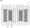
- First secondary coil 12 includes a second conductor 17 wound around first core 13. Second conductor 17 is wound around first leg 13a. Second conductor 17 may be wound around second core 14. Second conductor 17 may be wound around third leg 14a. First secondary coil 12 may be disposed inside first primary coil 11. First secondary coil 12 may be disposed between first primary coil 11 and first leg 13a and between first primary coil 11 and third leg 14a. Second conductor 17 may be a first conductive foil. In second conductor 17 formed of the first conductive foil, a power loss in first secondary coil 12, which results from the skin effect and the proximity effect in first secondary coil 12, can be reduced.
- first insulating member 15 covers first secondary coil 12.
- First insulating member 15 may seal first secondary coil 12.
- First secondary coil 12 may be molded with first insulating member 15.
- First insulating member 15 may be formed of a resin material, such as epoxy resin or polyurethane resin.
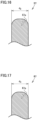
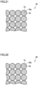
- first corner 17p has first radius of curvature r 1 of 0.1 mm, an increase in the electric field strength in first insulating member 15, which results from the concentration of electric field at first corner 17p, can be restrained, which can prevent a dielectric breakdown of first insulating member 15.
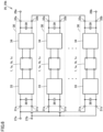
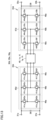
- AC/DC conversion circuits 34d are connected to first secondary coils 12 of transformation units 40 (three transformers 1, 1a, 1b, 1c). Specifically, first terminals of first secondary coils 12 of three transformers 1, 1a, 1b, 1c are connected to AC/DC conversion circuit 34d. Second terminals of first secondary coils 12 of three transformers 1, 1a, 1b, 1c are connected to each other.
- AC/DC conversion circuit 34d is a second three-phase bridge circuit.
- AC/DC conversion circuit 34d may be a second three-phase full-bridge circuit.
- AC/DC conversion circuit 34d may include second switching circuit 47d.
- First switching elements 41a, 41b, 41c, 41d, 41e, 41f and second switching elements 43a, 43b, 43c, 43d, 43e, 43f may be configured to operate at frequencies of 100 Hz or more, may be configured to operate at frequencies of 200 Hz or more, or may be configured to operate at frequencies of 1 kHz or more.
- First switching elements 41a, 41b, 41c, 41d, 41e, 41f and second switching elements 43a, 43b, 43c, 43d, 43e, 43f may be configured to operate at frequencies of 2 kHz of less.
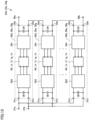
- Each of AC/DC conversion circuits 34d is connected to a corresponding one of first secondary coils 12 of three transformers 1, 1a, 1b, 1c and is a second three-phase bridge circuit.
- Primary terminals 31a, 31b of DC/DC converters 30d are connected in parallel with each other.
- Secondary terminals 32a, 32b of DC/DC converters 30d are connected in series with each other.
- Power converter 25d of the present Embodiment has improved dielectric breakdown voltage and improved power efficiency.
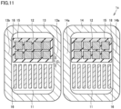
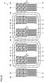
- Second insulating member 55 covers second secondary coil 52. Second insulating member 55 may seal second secondary coil 52. Second secondary coil 52 may be molded with second insulating member 55. Second insulating member 55 may be formed of a resin material, such as epoxy resin or polyurethane resin.
- Third insulating member 65 covers third secondary coil 62. Third insulating member 65 may seal third secondary coil 62. Third secondary coil 62 may be molded with third insulating member 65. Third insulating member 65 may be formed of a resin material, such as epoxy resin or polyurethane resin.
- second primary coil 51 and second secondary coil 52 may be arranged in the direction in which second leg 13b extends.
- Third primary coil 61 and third secondary coil 62 may be arranged in the direction in which fourth leg 14b extends.
- a gap G 2 between second primary coil 51 and second secondary coil 52 can be relatively large compared with transformer 1e.
- a gap G 3 between third primary coil 61 and third secondary coil 62 can be relatively large compared with transformer 1e.
- magnetic coupling between second primary coil 51 and second secondary coil 52 can be weak compared with transformer 1e.
- magnetic coupling between third primary coil 61 and third secondary coil 62 can be weak compared with transformer 1e.
- Transformer 1f has a relatively high leakage inductance compared with transformer 1e.
- a fourth conductor 58 is a second litz wire formed of a plurality of twisted second conductive strands 59.
- Second conductive strands 59 each have the shape of a circle having a second radius R 2 of 0.1 mm or more in the second cross-section.
- fourth conductor 58 has a second corner 58p having second radius of curvature r 2 which is defined by second radius R 2 of second conductive strand 59.
- Second radius R 2 may be equal to first radius R 1 , may be greater than first radius R 1 , or may be smaller than first radius R 1 .
- second primary coil 51 and second secondary coil 52 may be arranged in the direction in which second leg 13b extends.
- gap G 2 between second primary coil 51 and second secondary coil 52 can be relatively large compared with transformer 1g.
- magnetic coupling between second primary coil 51 and second secondary coil 52 can be weak compared with transformer 1g.
- third primary coil 61 and third secondary coil 62 may be arranged in the direction in which fourth leg 14b extends.
- gap G 3 between third primary coil 61 and third secondary coil 62 can be relatively large compared with transformer 1g.
- magnetic coupling between third primary coil 61 and third secondary coil 62 can be weak compared with transformer 1g.
- Transformer 1h thus has a relatively high leakage inductance compared with transformer 1g.
- first primary coil 11 when a voltage is applied to between primary terminals 31a, 31b, the voltage is applied to first primary coil 11 via DC/AC conversion circuit 33.
- First primary coil 11 applied with the voltage excites a magnetic flux in first leg 13a of first core 13 and third leg 14a of second core 14. This magnetic flux causes an induced voltage in first secondary coil 12. Since the first inductance of first primary coil 11 is equal to the second inductance of first secondary coil 12, the same magnetic flux as that of first primary coil 11 is excited also in first secondary coil 12, causing the induced voltage to be equal to the voltage applied to first secondary coil 12 by second switching circuit 47. This prevents a flow of reactive current through second switching circuit 47, thus preventing a power loss in second switching elements 43a, 43b, 43c, 43d.
- Embodiments 1 to 6 and the modifications thereof disclosed herein are illustrative and non-restrictive in every respect. At least two of Embodiments 1 to 6 and the modifications thereof disclosed herein may be combined within a range free of inconsistency or contradiction.
- the scope of the present invention is defined by the terms of the claims, rather than the description of the embodiments above, and is intended to include any modifications within the scope of the claims.
Landscapes
- Engineering & Computer Science (AREA)
- Power Engineering (AREA)
- Dc-Dc Converters (AREA)
- Coils Of Transformers For General Uses (AREA)
Claims (15)
- Leistungswandler (25, 25b, 25d, 25e, 25g), der Folgendes aufweist:- eine Mehrzahl von DC/DC-Wandlern (30, 30d, 30e, 30g);- ein Paar von DC-Primäranschlüssen (27a, 27b); und- ein Paar von DC-Sekundäranschlüssen (28a, 28b),wobei jeder der Mehrzahl von DC/DC-Wandlern (30, 30d, 30e, 30g) Folgendes aufweist:- einen Primäranschluss (31a, 31b),- eine DC/AC-Wandlungsschaltung (33, 33d), die mit dem Primäranschluss (31a, 31b) verbunden ist,- einen Transformator (1, 1a, 1b, 1c),- eine AC/DC-Wandlungsschaltung (34, 34d), und- einen Sekundäranschluss (32a, 32b), der mit derAC/DC-Wandlungsschaltung (34, 34d) verbunden ist,dadurch gekennzeichnet,dass der Transformator (1, 1a, 1b, 1c) Folgendes aufweist:- einen ersten Kern (13),- eine erste Primärspule (11), wobei die erste Primärspule (11) einen ersten Leiter (16) aufweist, der um den ersten Kern (13) gewickelt ist,- eine erste Sekundärspule (12), wobei die erste Sekundärspule (12) einen zweiten Leiter (17, 18) aufweist, der um den ersten Kern (13) gewickelt ist, und- ein erstes Isolierelement (15), das die erste Sekundärspule (12) bedeckt, wobei die erste Sekundärspule (12) im Vergleich zur ersten Primärspule (11) mit einer hohen Spannung beaufschlagt wird, undwobei der zweite Leiter (17, 18) in einem ersten Querschnitt des zweiten Leiters (17, 18) rechtwinklig zu einer Richtung, in der sich der zweite Leiter (17, 18) erstreckt, die Form eines ersten Polygons hat, und wobei eine erste Ecke des ersten Polygons einen ersten Krümmungsradius von 0,1 mm oder mehr hat.
- Leistungswandler (25, 25b, 25d, 25e, 25g) nach Anspruch 1,wobei die DC/AC-Wandlungsschaltung (33, 33d) mit der ersten Primärspule (11) verbunden ist und eine erste einphasige Brückenschaltung ist,die AC/DC-Wandlungsschaltung (34, 34d) mit der ersten Sekundärspule (12) verbunden ist und eine zweite einphasige Brückenschaltung ist,eine Mehrzahl von Primäranschlüssen (31a, 31b) der Mehrzahl von DC/DC-Wandlern (30, 30d, 30e, 30g) parallel zu dem Paar von DC-Primäranschlüssen (27a, 27b) geschaltet ist, undeine Mehrzahl von Sekundäranschlüssen (32a, 32b) der Mehrzahl von DC/DC-Wandlern (30, 30d, 30e, 30g) miteinander in Reihe geschaltet ist und zwischen dem Paar von DC-Sekundäranschlüssen (28a, 28b) in Reihe geschaltet ist.
- Leistungswandler (25, 25b, 25d, 25e, 25g) nach Anspruch 2,
wobei der zweite Leiter (17, 18) eine erste leitfähige Folie aufweist. - Leistungswandler (25, 25b, 25d, 25e, 25g) nach Anspruch 2,wobei der zweite Leiter (17, 18) eine erste Litze aufweist, die aus einer Mehrzahl von ersten leitfähigen verdrillten Strängen gebildet ist, undwobei die Mehrzahl von ersten leitfähigen Strängen jeweils die Form eines Kreises mit einem ersten Radius von 0,1 mm oder mehr im ersten Querschnitt hat.
- Leistungswandler (25, 25b, 25d, 25e, 25g) nach einem der Ansprüche 1 bis 4, wobei eine erste Induktivität der ersten Primärspule (11) gleich einer zweiten Induktivität der ersten Sekundärspule (12) ist.
- Leistungswandler (25, 25b, 25d, 25e, 25g) nach einem der Ansprüche 1 bis 5, der ferner einen zweiten Kern (14) aufweist,wobei der erste Kern (13) Folgendes aufweist:- einen ersten Schenkel (13a) und- einen zweiten Schenkel (13b), der dem ersten Schenkel (13a) gegenüberliegt, wobei der zweite Kern (14) Folgendes aufweist:- einen dritten Schenkel (14a), der dem ersten Schenkel (13a) zugewandt ist, und- einen vierten Schenkel (14b), der dem dritten Schenkel (14a) gegenüberliegt, wobei der erste Leiter (16) um den ersten Schenkel (13a) und den dritten Schenkel (14a) gewickelt ist, undwobei der zweite Leiter (17, 18) um den ersten Schenkel (13a) und den dritten Schenkel (14a) gewickelt ist.
- Leistungswandler (25, 25b, 25d, 25e, 25g) nach Anspruch 6,
wobei die erste Sekundärspule (12) innerhalb von der ersten Primärspule (11) angeordnet ist. - Leistungswandler (25, 25b, 25d, 25e, 25g) nach Anspruch 6,
wobei die erste Primärspule (11) und die erste Sekundärspule (12) in einer Richtung angeordnet sind, in der sich der erste Schenkel (13a) und der dritte Schenkel (14a) erstrecken. - Leistungswandler (25, 25b, 25d, 25e, 25g) nach einem der Ansprüche 6 bis 8, wobei der zweite Kern (14) aus einem zweiten amorphen magnetischen Material oder einem zweiten nanokristallinen magnetischen Material gebildet ist.
- Leistungswandler (25d, 25e, 25g) nach Anspruch 1,wobei der Transformator (1e, 1f, 1g, 1h) ferner einen zweiten Kern (14) aufweist, wobei der erste Kern (13) Folgendes aufweist:- einen ersten Schenkel (13a) und- einen zweiten Schenkel (13b), der dem ersten Schenkel (13a) gegenüberliegt, wobei der zweite Kern (14) Folgendes aufweist:- einen dritten Schenkel (14a), der dem ersten Schenkel (13a) zugewandt ist, und- einen vierten Schenkel (14b), der dem dritten Schenkel (14a) gegenüberliegt, wobei der erste Leiter (16) um den ersten Schenkel (13a) und den dritten Schenkel (14a) gewickelt ist,wobei der zweite Leiter (17, 18) um den ersten Schenkel (13a) und den dritten Schenkel (14a) gewickelt ist,wobei der Transformator (1e, 1f, 1g, 1h) ferner Folgendes aufweist:- eine zweite Primärspule (51), wobei die zweite Primärspule (51) einen dritten Leiter (56) aufweist, der um den zweiten Schenkel (13b) gewickelt ist,- eine zweite Sekundärspule (52), wobei die zweite Sekundärspule (52) einen vierten Leiter (57, 58) aufweist, der um den zweiten Schenkel (13b) gewickelt ist,- ein zweites Isolierelement (55), das die zweite Sekundärspule (52) bedeckt,- eine dritte Primärspule (61), wobei die dritte Primärspule (61) einen fünften Leiter (66) aufweist, der um den vierten Schenkel (14b) gewickelt ist,- eine dritte Sekundärspule (62), wobei die dritte Sekundärspule (62) einen sechsten Leiter (67, 68) aufweist, der um den vierten Schenkel (14b) gewickelt ist, und- ein drittes Isolierelement (65), das die dritte Sekundärspule (62) bedeckt, wobei die zweite Sekundärspule (52) mit einer hohen Spannung im Vergleich zur zweiten Primärspule (51) beaufschlagt wird,wobei die dritte Sekundärspule (62) mit einer hohen Spannung im Vergleich zur dritten Primärspule (61) beaufschlagt wird,wobei der vierte Leiter (57, 58) in einem zweiten Querschnitt des vierten Leiters (57, 58) rechtwinklig zu einer Richtung, in der sich der vierte Leiter (57, 58) erstreckt, die Form eines zweiten Polygons hat, und wobei eine zweite Ecke des zweiten Polygons einen Krümmungsradius von 0,1 mm oder mehr hat, wobei der sechste Leiter (67, 68) in einem dritten Querschnitt des sechsten Leiters (67, 68) rechtwinklig zu einer Richtung, in der sich der sechste Leiter (67, 68) erstreckt, die Form eines dritten Polygons hat, und wobei eine dritte Ecke des dritten Polygons einen dritten Krümmungsradius von 0,1 mm oder mehr hat, wobei die DC/AC-Wandlungsschaltung (33, 33d) mit der ersten Primärspule (11), der zweiten Primärspule (51) und der dritten Primärspule (61) verbunden ist und eine erste dreiphasige Brückenschaltung ist,wobei die AC/DC-Wandlungsschaltung (34, 34d) mit der ersten Sekundärspule (12), der zweiten Sekundärspule (52) und der dritten Sekundärspule (62) verbunden ist und eine zweite dreiphasige Brückenschaltung ist,wobei eine Mehrzahl von Primäranschlüssen (31a, 31b) der Mehrzahl von DC/DC-Wandlern (30, 30d, 30e, 30g) parallel zu dem Paar von DC-Primäranschlüssen (27a, 27b) geschaltet ist, undeine Mehrzahl von Sekundäranschlüssen (32a, 32b) der Mehrzahl von DC/DC-Wandlern (30, 30d, 30e, 30g) miteinander in Reihe geschaltet ist und zwischen dem Paar von DC-Sekundäranschlüssen (28a, 28b) in Reihe geschaltet ist.
- Leistungswandler (25d, 25e, 25g) nach Anspruch 10,
wobei der vierte Leiter (57, 58) eine zweite leitfähige Folie aufweist, und der sechste Leiter (67, 68) eine dritte leitfähige Folie aufweist. - Leistungswandler (25d, 25e, 25g) nach Anspruch 10,wobei der vierte Leiter (57, 58) eine zweite Litze aufweist, die aus einer Mehrzahl von zweiten leitfähigen verdrillten Strängen gebildet ist,der sechste Leiter (67, 68) eine dritte Litze aufweist, die aus einer Mehrzahl von dritten leitfähigen verdrillten Strängen gebildet ist,die Mehrzahl von zweiten leitfähigen Strängen jeweils die Form eines Kreises mit einem zweiten Radius von 0,1 mm oder mehr im zweiten Querschnitt hat und die Mehrzahl von dritten leitfähigen Strängen jeweils die Form eines Kreises mit einem dritten Radius von 0,1 mm oder mehr im dritten Querschnitt hat.
- Leistungswandler (25d, 25e, 25g) nach einem der Ansprüche 10 bis 12,wobei die zweite Sekundärspule (52) innerhalb von der zweiten Primärspule (51) angeordnet ist, unddie dritte Sekundärspule (62) innerhalb von der dritten Primärspule (61) angeordnet ist.
- Leistungswandler (25d, 25e, 25g) nach einem der Ansprüche 10 bis 12, wobei die zweite Primärspule (51) und die zweite Sekundärspule (52) in einer Richtung angeordnet sind, in der sich der zweite Schenkel (13b) erstreckt, und die dritte Primärspule (61) und die dritte Sekundärspule (62) in einer Richtung angeordnet sind, in der sich der vierte Schenkel (14b) erstreckt.
- Leistungswandler (25d, 25e, 25g) nach Anspruch 1,wobei jeder der Mehrzahl von DC/DC-Wandlern (30, 30d, 30e, 30g) eine Transformationseinheit (40) mit drei Transformatoren (1e, 1f, 1g, 1h) aufweist, wobei die DC/AC-Wandlungsschaltung (33, 33d) mit einer Mehrzahl von ersten Primärspulen (11) der drei Transformatoren (1e, 1f, 1g, 1h) verbunden ist und eine erste dreiphasige Brückenschaltung ist,wobei die AC/DC-Wandlungsschaltung (34, 34d) mit einer Mehrzahl von ersten Sekundärspulen (12) der drei Transformatoren (1e, 1f, 1g, 1h) verbunden ist und eine zweite dreiphasige Brückenschaltung ist,wobei eine Mehrzahl von Primäranschlüssen (31a, 31b) der Mehrzahl von DC/DC-Wandlern (30, 30d, 30e, 30g) parallel zueinander geschaltet ist, und wobei eine Mehrzahl von Sekundäranschlüssen (32a, 32b) der Mehrzahl von DC/DC-Wandlern (30, 30d, 30e, 30g) in Reihe miteinander geschaltet ist.
Applications Claiming Priority (2)
| Application Number | Priority Date | Filing Date | Title |
|---|---|---|---|
| JP2017212111 | 2017-11-01 | ||
| PCT/JP2018/025504 WO2019087466A1 (ja) | 2017-11-01 | 2018-07-05 | 変圧器及び電力変換装置 |
Publications (3)
| Publication Number | Publication Date |
|---|---|
| EP3706150A1 EP3706150A1 (de) | 2020-09-09 |
| EP3706150A4 EP3706150A4 (de) | 2021-02-17 |
| EP3706150B1 true EP3706150B1 (de) | 2023-09-20 |
Family
ID=66333496
Family Applications (1)
| Application Number | Title | Priority Date | Filing Date |
|---|---|---|---|
| EP18874496.5A Active EP3706150B1 (de) | 2017-11-01 | 2018-07-05 | Leistungswandler umfassend einen transformator |
Country Status (4)
| Country | Link |
|---|---|
| US (1) | US11290019B2 (de) |
| EP (1) | EP3706150B1 (de) |
| JP (1) | JP6725755B2 (de) |
| WO (1) | WO2019087466A1 (de) |
Families Citing this family (7)
| Publication number | Priority date | Publication date | Assignee | Title |
|---|---|---|---|---|
| EP3648130B1 (de) * | 2018-10-31 | 2021-07-07 | ABB Power Grids Switzerland AG | Transformator und verfahren zur herstellung eines transformators |
| CN111462996B (zh) * | 2020-05-18 | 2022-06-07 | 台达电子企业管理(上海)有限公司 | 磁性元件及电源装置 |
| CN113851303A (zh) * | 2020-06-28 | 2021-12-28 | 伊顿智能动力有限公司 | 高电流耦合绕组电磁部件 |
| CA3186203A1 (en) * | 2020-07-15 | 2022-01-20 | Mahdi S. ATTEIA | Dc to dc boost converter |
| CN114068153A (zh) | 2020-08-07 | 2022-02-18 | 伊顿智能动力有限公司 | 低轮廓高电流耦合绕组电磁部件 |
| JP7596927B2 (ja) * | 2021-05-24 | 2024-12-10 | 富士電機株式会社 | 電力変換装置およびトランス |
| JP2024067279A (ja) * | 2022-11-04 | 2024-05-17 | 株式会社日立産機システム | 静止電磁機器及び静止電磁機器を用いた双方向dc-dcコンバータ |
Family Cites Families (17)
| Publication number | Priority date | Publication date | Assignee | Title |
|---|---|---|---|---|
| JPS5863725U (ja) | 1981-10-23 | 1983-04-28 | 株式会社日立製作所 | モ−ルドコイル |
| JPS60145600U (ja) | 1984-03-06 | 1985-09-27 | 四国変圧器株式会社 | 放電灯点灯装置 |
| JPS62193103A (ja) | 1986-02-19 | 1987-08-25 | Fuji Electric Co Ltd | 絶縁コイル |
| US5027264A (en) | 1989-09-29 | 1991-06-25 | Wisconsin Alumni Research Foundation | Power conversion apparatus for DC/DC conversion using dual active bridges |
| JPH10163045A (ja) | 1996-11-29 | 1998-06-19 | Eye Lighting Syst Corp | 変圧器用鉄心、三相電源用変圧器及び放電灯安定器 |
| AT406921B (de) * | 1998-08-20 | 2000-10-25 | Asta Elektrodraht Gmbh | Elektrischer leiter |
| JP2002208527A (ja) * | 2001-01-12 | 2002-07-26 | Toko Inc | 漏れ磁束型電力変換トランス |
| JP2004119811A (ja) | 2002-09-27 | 2004-04-15 | Toshiba Corp | 静止誘導電気機器 |
| JP4977563B2 (ja) * | 2007-09-06 | 2012-07-18 | ニチコン株式会社 | 三相乾式変圧器 |
| JP5137749B2 (ja) * | 2008-08-28 | 2013-02-06 | 古河電気工業株式会社 | 巻線用絶縁電線およびコイルの製造方法 |
| WO2011008533A2 (en) | 2009-06-29 | 2011-01-20 | Gerald Leto | Multifunctional writing apparatus with capacitive touch screen stylus |
| JP5307105B2 (ja) | 2010-01-06 | 2013-10-02 | 株式会社神戸製鋼所 | 複合型巻線素子ならびにこれを用いた変圧器、変圧システムおよびノイズカットフィルタ用複合型巻線素子 |
| JP5939607B2 (ja) * | 2011-03-30 | 2016-06-22 | 株式会社Nttファシリティーズ | 電力変換システム、コンピュータ及びプログラム |
| FR2987190B1 (fr) * | 2012-02-22 | 2014-06-27 | Inst Polytechnique Grenoble | Convertisseur de tension |
| US10361023B2 (en) * | 2014-08-07 | 2019-07-23 | Nvidia Corporation | Magnetic power coupling to an integrated circuit module |
| JP2017117920A (ja) | 2015-12-24 | 2017-06-29 | 株式会社日立産機システム | モールド変圧器 |
| JP6416436B2 (ja) | 2016-03-22 | 2018-10-31 | 三菱電機株式会社 | 電力変換装置 |
-
2018
- 2018-07-05 EP EP18874496.5A patent/EP3706150B1/de active Active
- 2018-07-05 US US16/757,643 patent/US11290019B2/en active Active
- 2018-07-05 WO PCT/JP2018/025504 patent/WO2019087466A1/ja not_active Ceased
- 2018-07-05 JP JP2019520912A patent/JP6725755B2/ja active Active
Also Published As
| Publication number | Publication date |
|---|---|
| US11290019B2 (en) | 2022-03-29 |
| JP6725755B2 (ja) | 2020-07-22 |
| WO2019087466A1 (ja) | 2019-05-09 |
| EP3706150A4 (de) | 2021-02-17 |
| JPWO2019087466A1 (ja) | 2019-11-14 |
| US20200295665A1 (en) | 2020-09-17 |
| EP3706150A1 (de) | 2020-09-09 |
Similar Documents
| Publication | Publication Date | Title |
|---|---|---|
| EP3706150A1 (de) | Transformator und leistungswandlungsvorrichtung | |
| JP4800451B1 (ja) | 高周波トランス | |
| KR101259778B1 (ko) | 3상 고주파 트랜스포머 | |
| RU2115186C1 (ru) | Многофазный трансформатор | |
| US9583252B2 (en) | Transformer | |
| US9859713B2 (en) | Parallel inverters connected to one inductor | |
| CN116635958A (zh) | 具有改进的电磁屏蔽的线圈和变压器 | |
| JP4738545B1 (ja) | 高周波トランス | |
| CN211858327U (zh) | 电感结构、电抗装置和变压装置 | |
| CN116895444A (zh) | 用于连接到功率转换器的dc侧的共模扼流圈、滤波器装置和功率转换器 | |
| CN103151154A (zh) | 弧边三角形移相变压器 | |
| RU2337423C1 (ru) | Электрический высокочастотный трансформатор | |
| CN101952910A (zh) | 包括变压功能和谐波及电流不平衡改善功能的混合变压器及包括其的供电系统 | |
| CN109346291B (zh) | 一种绕组结构及变压器 | |
| EP4621811A1 (de) | Hochleistungs-hochstromtransformator | |
| US20240203637A1 (en) | Winding arrangement for transformer | |
| JPH036805A (ja) | タップ巻線付変圧器 | |
| EP2556584A1 (de) | Statischer stromwandler | |
| CN113506675B (zh) | 双变比变压器 | |
| RU2731209C1 (ru) | Устройство равномерного распределения однофазной нагрузки по фазам трехфазной сети | |
| CN214588368U (zh) | 一种变压器及隔离变流器 | |
| JP4629857B2 (ja) | 樹脂モールド変圧器 | |
| SU866591A1 (ru) | Трансформатор | |
| Anurag et al. | Matrix based Inductor Structure for MV Applications | |
| RU2421838C1 (ru) | Электрический высокочастотный трансформатор |
Legal Events
| Date | Code | Title | Description |
|---|---|---|---|
| STAA | Information on the status of an ep patent application or granted ep patent |
Free format text: STATUS: THE INTERNATIONAL PUBLICATION HAS BEEN MADE |
|
| PUAI | Public reference made under article 153(3) epc to a published international application that has entered the european phase |
Free format text: ORIGINAL CODE: 0009012 |
|
| STAA | Information on the status of an ep patent application or granted ep patent |
Free format text: STATUS: REQUEST FOR EXAMINATION WAS MADE |
|
| 17P | Request for examination filed |
Effective date: 20200424 |
|
| AK | Designated contracting states |
Kind code of ref document: A1 Designated state(s): AL AT BE BG CH CY CZ DE DK EE ES FI FR GB GR HR HU IE IS IT LI LT LU LV MC MK MT NL NO PL PT RO RS SE SI SK SM TR |
|
| AX | Request for extension of the european patent |
Extension state: BA ME |
|
| A4 | Supplementary search report drawn up and despatched |
Effective date: 20210119 |
|
| DAV | Request for validation of the european patent (deleted) | ||
| DAX | Request for extension of the european patent (deleted) | ||
| RIC1 | Information provided on ipc code assigned before grant |
Ipc: H01F 30/10 20060101AFI20210113BHEP Ipc: H02M 3/00 20060101ALI20210113BHEP Ipc: H01F 41/12 20060101ALI20210113BHEP Ipc: H01F 27/28 20060101ALI20210113BHEP |
|
| GRAP | Despatch of communication of intention to grant a patent |
Free format text: ORIGINAL CODE: EPIDOSNIGR1 |
|
| STAA | Information on the status of an ep patent application or granted ep patent |
Free format text: STATUS: GRANT OF PATENT IS INTENDED |
|
| INTG | Intention to grant announced |
Effective date: 20220321 |
|
| GRAJ | Information related to disapproval of communication of intention to grant by the applicant or resumption of examination proceedings by the epo deleted |
Free format text: ORIGINAL CODE: EPIDOSDIGR1 |
|
| STAA | Information on the status of an ep patent application or granted ep patent |
Free format text: STATUS: REQUEST FOR EXAMINATION WAS MADE |
|
| INTC | Intention to grant announced (deleted) | ||
| GRAJ | Information related to disapproval of communication of intention to grant by the applicant or resumption of examination proceedings by the epo deleted |
Free format text: ORIGINAL CODE: EPIDOSDIGR1 |
|
| GRAP | Despatch of communication of intention to grant a patent |
Free format text: ORIGINAL CODE: EPIDOSNIGR1 |
|
| GRAP | Despatch of communication of intention to grant a patent |
Free format text: ORIGINAL CODE: EPIDOSNIGR1 |
|
| STAA | Information on the status of an ep patent application or granted ep patent |
Free format text: STATUS: GRANT OF PATENT IS INTENDED |
|
| INTG | Intention to grant announced |
Effective date: 20230403 |
|
| P01 | Opt-out of the competence of the unified patent court (upc) registered |
Effective date: 20230601 |
|
| GRAS | Grant fee paid |
Free format text: ORIGINAL CODE: EPIDOSNIGR3 |
|
| GRAA | (expected) grant |
Free format text: ORIGINAL CODE: 0009210 |
|
| STAA | Information on the status of an ep patent application or granted ep patent |
Free format text: STATUS: THE PATENT HAS BEEN GRANTED |
|
| AK | Designated contracting states |
Kind code of ref document: B1 Designated state(s): AL AT BE BG CH CY CZ DE DK EE ES FI FR GB GR HR HU IE IS IT LI LT LU LV MC MK MT NL NO PL PT RO RS SE SI SK SM TR |
|
| REG | Reference to a national code |
Ref country code: GB Ref legal event code: FG4D |
|
| REG | Reference to a national code |
Ref country code: CH Ref legal event code: EP |
|
| REG | Reference to a national code |
Ref country code: IE Ref legal event code: FG4D |
|
| REG | Reference to a national code |
Ref country code: DE Ref legal event code: R096 Ref document number: 602018058060 Country of ref document: DE |
|
| REG | Reference to a national code |
Ref country code: SE Ref legal event code: TRGR |
|
| REG | Reference to a national code |
Ref country code: LT Ref legal event code: MG9D |
|
| PG25 | Lapsed in a contracting state [announced via postgrant information from national office to epo] |
Ref country code: GR Free format text: LAPSE BECAUSE OF FAILURE TO SUBMIT A TRANSLATION OF THE DESCRIPTION OR TO PAY THE FEE WITHIN THE PRESCRIBED TIME-LIMIT Effective date: 20231221 |
|
| REG | Reference to a national code |
Ref country code: NL Ref legal event code: MP Effective date: 20230920 |
|
| PG25 | Lapsed in a contracting state [announced via postgrant information from national office to epo] |
Ref country code: RS Free format text: LAPSE BECAUSE OF FAILURE TO SUBMIT A TRANSLATION OF THE DESCRIPTION OR TO PAY THE FEE WITHIN THE PRESCRIBED TIME-LIMIT Effective date: 20230920 Ref country code: NO Free format text: LAPSE BECAUSE OF FAILURE TO SUBMIT A TRANSLATION OF THE DESCRIPTION OR TO PAY THE FEE WITHIN THE PRESCRIBED TIME-LIMIT Effective date: 20231220 Ref country code: LV Free format text: LAPSE BECAUSE OF FAILURE TO SUBMIT A TRANSLATION OF THE DESCRIPTION OR TO PAY THE FEE WITHIN THE PRESCRIBED TIME-LIMIT Effective date: 20230920 Ref country code: LT Free format text: LAPSE BECAUSE OF FAILURE TO SUBMIT A TRANSLATION OF THE DESCRIPTION OR TO PAY THE FEE WITHIN THE PRESCRIBED TIME-LIMIT Effective date: 20230920 Ref country code: HR Free format text: LAPSE BECAUSE OF FAILURE TO SUBMIT A TRANSLATION OF THE DESCRIPTION OR TO PAY THE FEE WITHIN THE PRESCRIBED TIME-LIMIT Effective date: 20230920 Ref country code: GR Free format text: LAPSE BECAUSE OF FAILURE TO SUBMIT A TRANSLATION OF THE DESCRIPTION OR TO PAY THE FEE WITHIN THE PRESCRIBED TIME-LIMIT Effective date: 20231221 Ref country code: FI Free format text: LAPSE BECAUSE OF FAILURE TO SUBMIT A TRANSLATION OF THE DESCRIPTION OR TO PAY THE FEE WITHIN THE PRESCRIBED TIME-LIMIT Effective date: 20230920 |
|
| REG | Reference to a national code |
Ref country code: AT Ref legal event code: MK05 Ref document number: 1614074 Country of ref document: AT Kind code of ref document: T Effective date: 20230920 |
|
| PG25 | Lapsed in a contracting state [announced via postgrant information from national office to epo] |
Ref country code: NL Free format text: LAPSE BECAUSE OF FAILURE TO SUBMIT A TRANSLATION OF THE DESCRIPTION OR TO PAY THE FEE WITHIN THE PRESCRIBED TIME-LIMIT Effective date: 20230920 |
|
| PG25 | Lapsed in a contracting state [announced via postgrant information from national office to epo] |
Ref country code: IS Free format text: LAPSE BECAUSE OF FAILURE TO SUBMIT A TRANSLATION OF THE DESCRIPTION OR TO PAY THE FEE WITHIN THE PRESCRIBED TIME-LIMIT Effective date: 20240120 |
|
| PG25 | Lapsed in a contracting state [announced via postgrant information from national office to epo] |
Ref country code: AT Free format text: LAPSE BECAUSE OF FAILURE TO SUBMIT A TRANSLATION OF THE DESCRIPTION OR TO PAY THE FEE WITHIN THE PRESCRIBED TIME-LIMIT Effective date: 20230920 |
|
| PG25 | Lapsed in a contracting state [announced via postgrant information from national office to epo] |
Ref country code: ES Free format text: LAPSE BECAUSE OF FAILURE TO SUBMIT A TRANSLATION OF THE DESCRIPTION OR TO PAY THE FEE WITHIN THE PRESCRIBED TIME-LIMIT Effective date: 20230920 |
|
| PG25 | Lapsed in a contracting state [announced via postgrant information from national office to epo] |
Ref country code: SM Free format text: LAPSE BECAUSE OF FAILURE TO SUBMIT A TRANSLATION OF THE DESCRIPTION OR TO PAY THE FEE WITHIN THE PRESCRIBED TIME-LIMIT Effective date: 20230920 Ref country code: RO Free format text: LAPSE BECAUSE OF FAILURE TO SUBMIT A TRANSLATION OF THE DESCRIPTION OR TO PAY THE FEE WITHIN THE PRESCRIBED TIME-LIMIT Effective date: 20230920 Ref country code: IS Free format text: LAPSE BECAUSE OF FAILURE TO SUBMIT A TRANSLATION OF THE DESCRIPTION OR TO PAY THE FEE WITHIN THE PRESCRIBED TIME-LIMIT Effective date: 20240120 Ref country code: ES Free format text: LAPSE BECAUSE OF FAILURE TO SUBMIT A TRANSLATION OF THE DESCRIPTION OR TO PAY THE FEE WITHIN THE PRESCRIBED TIME-LIMIT Effective date: 20230920 Ref country code: EE Free format text: LAPSE BECAUSE OF FAILURE TO SUBMIT A TRANSLATION OF THE DESCRIPTION OR TO PAY THE FEE WITHIN THE PRESCRIBED TIME-LIMIT Effective date: 20230920 Ref country code: CZ Free format text: LAPSE BECAUSE OF FAILURE TO SUBMIT A TRANSLATION OF THE DESCRIPTION OR TO PAY THE FEE WITHIN THE PRESCRIBED TIME-LIMIT Effective date: 20230920 Ref country code: AT Free format text: LAPSE BECAUSE OF FAILURE TO SUBMIT A TRANSLATION OF THE DESCRIPTION OR TO PAY THE FEE WITHIN THE PRESCRIBED TIME-LIMIT Effective date: 20230920 Ref country code: SK Free format text: LAPSE BECAUSE OF FAILURE TO SUBMIT A TRANSLATION OF THE DESCRIPTION OR TO PAY THE FEE WITHIN THE PRESCRIBED TIME-LIMIT Effective date: 20230920 Ref country code: PT Free format text: LAPSE BECAUSE OF FAILURE TO SUBMIT A TRANSLATION OF THE DESCRIPTION OR TO PAY THE FEE WITHIN THE PRESCRIBED TIME-LIMIT Effective date: 20240122 |
|
| PG25 | Lapsed in a contracting state [announced via postgrant information from national office to epo] |
Ref country code: PL Free format text: LAPSE BECAUSE OF FAILURE TO SUBMIT A TRANSLATION OF THE DESCRIPTION OR TO PAY THE FEE WITHIN THE PRESCRIBED TIME-LIMIT Effective date: 20230920 Ref country code: IT Free format text: LAPSE BECAUSE OF FAILURE TO SUBMIT A TRANSLATION OF THE DESCRIPTION OR TO PAY THE FEE WITHIN THE PRESCRIBED TIME-LIMIT Effective date: 20230920 |
|
| REG | Reference to a national code |
Ref country code: DE Ref legal event code: R097 Ref document number: 602018058060 Country of ref document: DE |
|
| PG25 | Lapsed in a contracting state [announced via postgrant information from national office to epo] |
Ref country code: DK Free format text: LAPSE BECAUSE OF FAILURE TO SUBMIT A TRANSLATION OF THE DESCRIPTION OR TO PAY THE FEE WITHIN THE PRESCRIBED TIME-LIMIT Effective date: 20230920 |
|
| PLBE | No opposition filed within time limit |
Free format text: ORIGINAL CODE: 0009261 |
|
| STAA | Information on the status of an ep patent application or granted ep patent |
Free format text: STATUS: NO OPPOSITION FILED WITHIN TIME LIMIT |
|
| PG25 | Lapsed in a contracting state [announced via postgrant information from national office to epo] |
Ref country code: DK Free format text: LAPSE BECAUSE OF FAILURE TO SUBMIT A TRANSLATION OF THE DESCRIPTION OR TO PAY THE FEE WITHIN THE PRESCRIBED TIME-LIMIT Effective date: 20230920 |
|
| 26N | No opposition filed |
Effective date: 20240621 |
|
| PG25 | Lapsed in a contracting state [announced via postgrant information from national office to epo] |
Ref country code: SI Free format text: LAPSE BECAUSE OF FAILURE TO SUBMIT A TRANSLATION OF THE DESCRIPTION OR TO PAY THE FEE WITHIN THE PRESCRIBED TIME-LIMIT Effective date: 20230920 |
|
| PG25 | Lapsed in a contracting state [announced via postgrant information from national office to epo] |
Ref country code: SI Free format text: LAPSE BECAUSE OF FAILURE TO SUBMIT A TRANSLATION OF THE DESCRIPTION OR TO PAY THE FEE WITHIN THE PRESCRIBED TIME-LIMIT Effective date: 20230920 |
|
| PG25 | Lapsed in a contracting state [announced via postgrant information from national office to epo] |
Ref country code: BG Free format text: LAPSE BECAUSE OF FAILURE TO SUBMIT A TRANSLATION OF THE DESCRIPTION OR TO PAY THE FEE WITHIN THE PRESCRIBED TIME-LIMIT Effective date: 20230920 |
|
| PG25 | Lapsed in a contracting state [announced via postgrant information from national office to epo] |
Ref country code: BG Free format text: LAPSE BECAUSE OF FAILURE TO SUBMIT A TRANSLATION OF THE DESCRIPTION OR TO PAY THE FEE WITHIN THE PRESCRIBED TIME-LIMIT Effective date: 20230920 |
|
| PG25 | Lapsed in a contracting state [announced via postgrant information from national office to epo] |
Ref country code: MC Free format text: LAPSE BECAUSE OF FAILURE TO SUBMIT A TRANSLATION OF THE DESCRIPTION OR TO PAY THE FEE WITHIN THE PRESCRIBED TIME-LIMIT Effective date: 20230920 |
|
| REG | Reference to a national code |
Ref country code: CH Ref legal event code: PL |
|
| PG25 | Lapsed in a contracting state [announced via postgrant information from national office to epo] |
Ref country code: LU Free format text: LAPSE BECAUSE OF NON-PAYMENT OF DUE FEES Effective date: 20240705 |
|
| PG25 | Lapsed in a contracting state [announced via postgrant information from national office to epo] |
Ref country code: LU Free format text: LAPSE BECAUSE OF NON-PAYMENT OF DUE FEES Effective date: 20240705 |
|
| PG25 | Lapsed in a contracting state [announced via postgrant information from national office to epo] |
Ref country code: CH Free format text: LAPSE BECAUSE OF NON-PAYMENT OF DUE FEES Effective date: 20240731 Ref country code: BE Free format text: LAPSE BECAUSE OF NON-PAYMENT OF DUE FEES Effective date: 20240731 |
|
| PG25 | Lapsed in a contracting state [announced via postgrant information from national office to epo] |
Ref country code: FR Free format text: LAPSE BECAUSE OF NON-PAYMENT OF DUE FEES Effective date: 20240731 |
|
| REG | Reference to a national code |
Ref country code: BE Ref legal event code: MM Effective date: 20240731 |
|
| PGFP | Annual fee paid to national office [announced via postgrant information from national office to epo] |
Ref country code: GB Payment date: 20250529 Year of fee payment: 8 |
|
| PG25 | Lapsed in a contracting state [announced via postgrant information from national office to epo] |
Ref country code: IE Free format text: LAPSE BECAUSE OF NON-PAYMENT OF DUE FEES Effective date: 20240705 |
|
| PGFP | Annual fee paid to national office [announced via postgrant information from national office to epo] |
Ref country code: SE Payment date: 20250528 Year of fee payment: 8 |
|
| PGFP | Annual fee paid to national office [announced via postgrant information from national office to epo] |
Ref country code: DE Payment date: 20250528 Year of fee payment: 8 |
|
| PG25 | Lapsed in a contracting state [announced via postgrant information from national office to epo] |
Ref country code: CY Free format text: LAPSE BECAUSE OF FAILURE TO SUBMIT A TRANSLATION OF THE DESCRIPTION OR TO PAY THE FEE WITHIN THE PRESCRIBED TIME-LIMIT; INVALID AB INITIO Effective date: 20180705 |
|
| PG25 | Lapsed in a contracting state [announced via postgrant information from national office to epo] |
Ref country code: HU Free format text: LAPSE BECAUSE OF FAILURE TO SUBMIT A TRANSLATION OF THE DESCRIPTION OR TO PAY THE FEE WITHIN THE PRESCRIBED TIME-LIMIT; INVALID AB INITIO Effective date: 20180705 |