EP3701548B1 - Leichtes kohlenstoffnanoröhrchenkabel mit einem paar plattierter verdrillter drähte - Google Patents
Leichtes kohlenstoffnanoröhrchenkabel mit einem paar plattierter verdrillter drähte Download PDFInfo
- Publication number
- EP3701548B1 EP3701548B1 EP18789534.7A EP18789534A EP3701548B1 EP 3701548 B1 EP3701548 B1 EP 3701548B1 EP 18789534 A EP18789534 A EP 18789534A EP 3701548 B1 EP3701548 B1 EP 3701548B1
- Authority
- EP
- European Patent Office
- Prior art keywords
- cnt
- cable
- approximately
- wire
- sub
- Prior art date
- Legal status (The legal status is an assumption and is not a legal conclusion. Google has not performed a legal analysis and makes no representation as to the accuracy of the status listed.)
- Active
Links
Images


Classifications
-
- H—ELECTRICITY
- H01—ELECTRIC ELEMENTS
- H01B—CABLES; CONDUCTORS; INSULATORS; SELECTION OF MATERIALS FOR THEIR CONDUCTIVE, INSULATING OR DIELECTRIC PROPERTIES
- H01B7/00—Insulated conductors or cables characterised by their form
- H01B7/17—Protection against damage caused by external factors, e.g. sheaths or armouring
- H01B7/18—Protection against damage caused by wear, mechanical force or pressure; Sheaths; Armouring
-
- C—CHEMISTRY; METALLURGY
- C01—INORGANIC CHEMISTRY
- C01B—NON-METALLIC ELEMENTS; COMPOUNDS THEREOF; METALLOIDS OR COMPOUNDS THEREOF NOT COVERED BY SUBCLASS C01C
- C01B32/00—Carbon; Compounds thereof
- C01B32/15—Nano-sized carbon materials
- C01B32/158—Carbon nanotubes
- C01B32/168—After-treatment
-
- C—CHEMISTRY; METALLURGY
- C25—ELECTROLYTIC OR ELECTROPHORETIC PROCESSES; APPARATUS THEREFOR
- C25D—PROCESSES FOR THE ELECTROLYTIC OR ELECTROPHORETIC PRODUCTION OF COATINGS; ELECTROFORMING; APPARATUS THEREFOR
- C25D3/00—Electroplating: Baths therefor
- C25D3/02—Electroplating: Baths therefor from solutions
- C25D3/38—Electroplating: Baths therefor from solutions of copper
-
- C—CHEMISTRY; METALLURGY
- C25—ELECTROLYTIC OR ELECTROPHORETIC PROCESSES; APPARATUS THEREFOR
- C25D—PROCESSES FOR THE ELECTROLYTIC OR ELECTROPHORETIC PRODUCTION OF COATINGS; ELECTROFORMING; APPARATUS THEREFOR
- C25D5/00—Electroplating characterised by the process; Pretreatment or after-treatment of workpieces
- C25D5/54—Electroplating of non-metallic surfaces
-
- C—CHEMISTRY; METALLURGY
- C25—ELECTROLYTIC OR ELECTROPHORETIC PROCESSES; APPARATUS THEREFOR
- C25D—PROCESSES FOR THE ELECTROLYTIC OR ELECTROPHORETIC PRODUCTION OF COATINGS; ELECTROFORMING; APPARATUS THEREFOR
- C25D7/00—Electroplating characterised by the article coated
- C25D7/06—Wires; Strips; Foils
- C25D7/0607—Wires
-
- H—ELECTRICITY
- H01—ELECTRIC ELEMENTS
- H01B—CABLES; CONDUCTORS; INSULATORS; SELECTION OF MATERIALS FOR THEIR CONDUCTIVE, INSULATING OR DIELECTRIC PROPERTIES
- H01B1/00—Conductors or conductive bodies characterised by the conductive materials; Selection of materials as conductors
- H01B1/04—Conductors or conductive bodies characterised by the conductive materials; Selection of materials as conductors mainly consisting of carbon-silicon compounds, carbon or silicon
-
- H—ELECTRICITY
- H01—ELECTRIC ELEMENTS
- H01B—CABLES; CONDUCTORS; INSULATORS; SELECTION OF MATERIALS FOR THEIR CONDUCTIVE, INSULATING OR DIELECTRIC PROPERTIES
- H01B11/00—Communication cables or conductors
- H01B11/18—Coaxial cables; Analogous cables having more than one inner conductor within a common outer conductor
- H01B11/20—Cables having a multiplicity of coaxial lines
-
- H—ELECTRICITY
- H01—ELECTRIC ELEMENTS
- H01B—CABLES; CONDUCTORS; INSULATORS; SELECTION OF MATERIALS FOR THEIR CONDUCTIVE, INSULATING OR DIELECTRIC PROPERTIES
- H01B13/00—Apparatus or processes specially adapted for manufacturing conductors or cables
- H01B13/02—Stranding-up
- H01B13/0207—Details; Auxiliary devices
-
- H—ELECTRICITY
- H01—ELECTRIC ELEMENTS
- H01B—CABLES; CONDUCTORS; INSULATORS; SELECTION OF MATERIALS FOR THEIR CONDUCTIVE, INSULATING OR DIELECTRIC PROPERTIES
- H01B13/00—Apparatus or processes specially adapted for manufacturing conductors or cables
- H01B13/06—Insulating conductors or cables
-
- H—ELECTRICITY
- H01—ELECTRIC ELEMENTS
- H01B—CABLES; CONDUCTORS; INSULATORS; SELECTION OF MATERIALS FOR THEIR CONDUCTIVE, INSULATING OR DIELECTRIC PROPERTIES
- H01B13/00—Apparatus or processes specially adapted for manufacturing conductors or cables
- H01B13/22—Sheathing; Armouring; Screening; Applying other protective layers
- H01B13/222—Sheathing; Armouring; Screening; Applying other protective layers by electro-plating
-
- H—ELECTRICITY
- H01—ELECTRIC ELEMENTS
- H01B—CABLES; CONDUCTORS; INSULATORS; SELECTION OF MATERIALS FOR THEIR CONDUCTIVE, INSULATING OR DIELECTRIC PROPERTIES
- H01B7/00—Insulated conductors or cables characterised by their form
- H01B7/02—Disposition of insulation
- H01B7/0208—Cables with several layers of insulating material
- H01B7/0216—Two layers
-
- H—ELECTRICITY
- H01—ELECTRIC ELEMENTS
- H01B—CABLES; CONDUCTORS; INSULATORS; SELECTION OF MATERIALS FOR THEIR CONDUCTIVE, INSULATING OR DIELECTRIC PROPERTIES
- H01B11/00—Communication cables or conductors
- H01B11/002—Pair constructions
Definitions
- This invention relates to a carbon nanotube cable and to a method for making a carbon nanotube cable.
- hybrid conductors which may be used in electrical or thermal applications, or combinations of both.
- One method of fabricating such hybrid conductors includes complexing conductive metal elements (e.g., silver, gold, copper), transition metal elements, alloys, wires, or combinations thereof, with carbon nanotube materials.
- the hybrid conductors may be formed by doping the carbon nanotube materials in salt solutions.
- a carbon nanotube (CNT) cable includes: a pair of plated twisted wires, each wire comprising one or more sub-cores, at least one sub-core comprising CNT yarn; the CNT yarn being chemically pretreated using chlorosulfonic acid; a dielectric surrounding the plated twisted wires; and an electrical layer surrounding the dielectric, the electrical layer shielding the CNT cable.
- a method for making a carbon nanotube (CNT) cable includes:, depositing plating using a controlled deposition rate, so as to surround a pair of wires, each wire comprising one or more sub-cores, at least one sub-core comprising CNT yarn; chemically pretreating the CNT yarn using chlorosulfonic acid; twisting the plated wires together; and surrounding the plated twisted wires with an electrical layer that shields the plated twisted wires, thereby creating the CNT cable.
- a CNT yarn cable is provided.
- a CNT cable is provided.
- a strong CNT cable is provided.
- a lightweight CNT cable is provided.
- a strong, lightweight CNT cable is provided.
- a resilient CNT cable is provided.
- a cable is provided having low radio frequency (RF) insertion loss.
- RF radio frequency
- a cable is provided having an RF insertion loss less than or equal to approximately 2.0 decibels per foot at a frequency of approximately 1 Gigahertz.
- a cable is provided having an RF insertion loss less than or equal to approximately 4.0 decibels per foot at a frequency of approximately 4 Gigahertz.
- a cable is provided having an insertion loss equivalent to the insertion loss of a solid copper wire.
- a cable is provided having high electrical conductivity.
- Figure 1 is a photograph 100 of a plated twisted wire 110 comprising one or more sub-cores, at least one sub-core comprising CNT yarn.
- FIGS 2A-2D are a set of four schematic drawings showing components of a CNT cable 200.
- the CNT cable 200 comprises a 28 American Wire Gauge (AWG) high speed CNT cable 200.
- AVG American Wire Gauge
- the CNT cable comprises a pair of twisted wires, a first twisted wire 210A and a second twisted wire 210B.
- the twisted wires 210A, 210B are shielded by the shield 220 that forms an electrical layer 220 of the CNT cable 200.
- the electrical layer 220 comprises an external surface 220 of the CNT cable 200.
- the electrical layer 200 is surrounded by a physical layer (not shown).
- the electrical layer 200 is surrounded by a braid (not shown), the braid configured to protect the electrical layer 200 from abrasion.
- At least one of the twisted, shielded wires 210A, 210B comprises a core.
- the first twisted wire 210A comprises a first core 230A.
- the second twisted wire 210B comprises a second core 230B.
- the first twisted wire 210A comprises a first core 230A
- the second twisted wire 210B comprises a second core 230B.
- at least one of the twisted shielded wires 210A, 210B has a desired number of sub-cores.
- the first core 230A is surrounded by first plating 240A.
- the second core 230B is surrounded by second plating 240B.
- one or more of the first plating 240A and the second plating 240B comprises copper plating.
- one or more of the first copper plating 240A and the second copper plating 240B comprises electroplated copper plating.
- one or more of the first plating 240A and the second plating 240B comprises silver plating.
- one or more of the first plating 240A and the second plating 240B comprises gold plating.
- the first core 230A is surrounded by a first copper plating 240A.
- the second core 230B is surrounded by a second copper plating 240B.
- one or more of the first copper plating 240A and the second copper plating 240B has a thickness of up to approximately 15 microns.
- the first copper plating 240A forms a first plated perimeter that runs around the outside of the surface formed by the three sub-cores 250A, 250B, and 250C.
- the second copper plating 240B forms a second plated perimeter that runs around the outside of the surface formed by the three sub-cores 250D, 250E, and 250F.
- first core 230A and the second core 230B comprises a multi-component core.
- first core 230A comprises a triaxial first core 230A comprising three sub-cores 250A, 250B, and 250C.
- the three sub-cores 250A, 250B, and 250C are twisted together.
- the second core 230B comprises a triaxial second core 230B comprising three sub-cores 250D, 250E, and 250F.
- the three sub-cores 250D, 250E, and 250F are twisted together.
- one or more of the sub-cores 250A-250F comprises yarn.
- one or more of the sub-cores 250A-250F comprises CNT yarn.
- one or more of the first sub-cores 250A-250F comprises chemically stretched CNT yarn (CSY).
- CSY pretreatment comprises an acid wash that uses chlorosulfonic acid to provide an optimal template to maximize conductivity of the plating layer.
- CSY pretreatment acid dopes semi-conducting CNT, thereby increasing conductivity.
- CSY also densifies the yarn.
- CSY also improves CNT network connectivity.
- the three sub-cores 250A, 250B, and 250C are twisted together to form a first twisted wire 210A of a desired gauge.
- a desired gauge For example, at least one of the three sub-cores 250A, 250B, and 250C has a desired approximate diameter.
- seven 1.5 tex (1.5g/Km) sub-cores (not shown) are twisted together to form a 28 American Wire Gauge (28AWG [.08sq mm]) first twisted wire 210A.
- Figure 2B shows an alternative embodiment of the CNT cable 200 in which the first twisted wire 210A comprises one sub-core 250A and the second twisted wire 210B comprises one sub-core 250B. Also shown are the shield 220, the first core 230A, the second core 230B, the first plated perimeter 240A and the second plated perimeter 240B.
- Figure 2C shows an alternative embodiment of the CNT cable 200 in which the first twisted wire 210A comprises four sub-cores 250A-250D and the second twisted wire 210B comprises four sub-cores 250E-250H. Also shown are the shield 220, the first core 230A, the second core 230B, the first plated perimeter 240A and the second plated perimeter 240B.
- Figure 2D shows an alternative embodiment of the CNT cable 200 in which the first twisted wire 210A comprises seven sub-cores 250A-250G and the second twisted wire 210B comprises four sub-cores 250H-250N. Also shown are the shield 220, the first core 230A, the second core 230B, the first plated perimeter 240A and the second plated perimeter 240B.
- An optimal yarn configuration comprises 28AWG [.08sq mm] CNT wire comprising four sub-cores. This configuration provides an excellent balance between competing considerations of maximizing plated perimeter and minimizing number of sub-cores.
- Embodiments of the invention have a conductivity above approximately 10 megasiemens per meter (MS/m). Embodiments of the invention have a conductivity above approximately 20 MS/m. Embodiments of the invention have a conductivity of approximately 20 MS/m to 58.5 MS/m.
- the fiber is lightweight. Preferably, the fiber has high tensile strength.
- Figures 3A-3D are a set of four micrographs showing a prior art CNT wire, a CNT wire that is copper plated according to embodiments of the invention, a CNT wire pretreated according to embodiments of the invention by performing an acid wash using chemically stretched CNT yarn (CSY), and a CSY pretreated CNT wire after copper plating according to embodiments of the invention.
- CSY chemically stretched CNT yarn
- Figure 3A is a micrograph of a prior art bare 28 American Wire Gauge (28AWG [.08sq mm]) CNT wire with a linear density of approximately 1.5 tex (1.5 grams per kilometer).
- Figure 3B is a micrograph of a 28AWG [.08sq mm] CNT wire with a linear density of approximately 1.5 tex (1.5g/Km) that is copper plated according to embodiments of the invention.
- Figure 3C is a micrograph of a bare 28AWG [.08sq mm] CNT wire with a linear density of approximately 10 tex (10g/Km) that is pretreated according to embodiments of the invention using CSY.
- Figure 3D is a micrograph of a 28AWG [.08sq mm] CNT wire with a linear density of approximately 10 tex (10g/Km) that is pretreated using CSY and is copper plated according to embodiments of the invention.
- CSY pretreatment produces yarn with a surface comprising substantially no loose CNT fibers that act as nucleation sites for large-scale surface defects during electroplating.
- CSY pretreatment of yarn according to embodiments of the invention produces yarn having minimal defects and also minimal surface roughness that does not contribute to a final surface roughness of a plated surface. Surface roughness of plated layer appears to be a function of conditions of an electroplating process used in operating the invention.
- Pretreatment with CSY according to embodiments of the invention results in an ideal, smooth substrate for electroplating the wire.
- CSY pretreatment also increases conductivity of the CNT cable.
- Figures 4A-4H are a set of eight micrographs showing both small-scale surface roughness and large-scale surface defects for both 24 American Wire Gauge (24AWG [0.25sq mm]) wire with an average grain size of approximately 1.8 microns and 28 American Wire Gauge (28AWG [.08sq mm]) wire with an average grain size of approximately 7.2 microns.
- the CNT cable comprises a pair of twisted wires, each wire having a grain size less than or equal to approximately 10 microns.
- the CNT cable comprises a pair of twisted wires, each wire having a grain size less than or equal to approximately 3 microns.
- Small-scale surface roughness means roughness visible using a magnification of approximately 2000 times.
- Large-scale surface defects means surface defects visible using a magnification of approximately 100 times.
- Figure 4A is a micrograph of small-scale surface roughness for embodiments of the invention using 24AWG [0.25sq mm] [0.25sq mm] wire with an average grain size of 1.8 microns and a low current.
- Figure 4B is a micrograph of small-scale surface roughness for embodiments of the invention using 24AWG [0.25sq mm] wire with an average grain size of 1.8 microns and a high current.
- Figure 4C is a micrograph of large-scale surface defects for embodiments of the invention using 24AWG [0.25sq mm] wire with an average grain size of 1.8 microns and a low current.
- Figure 4D is a micrograph of large-scale surface defects for embodiments of the invention using 24AWG [0.25sq mm] wire with an average grain size of 1.8 microns and a high current.
- Figure 4E is a micrograph of small-scale surface roughness for embodiments of the invention using 28AWG [.08sq mm] wire with an average grain size of 7.2 microns and a low current.
- Figure 4F is a micrograph of small-scale surface roughness for embodiments of the invention using 28AWG [.08sq mm] wire with an average grain size of 7.2 microns and a high current.
- Figure 4G is a micrograph of large-scale surface defects for embodiments of the invention using 28AWG [.08sq mm] wire with an average grain size of 7.2 microns and a low current.
- Figure 4H is a micrograph of large-scale surface defects for embodiments of the invention using 28AWG [.08sq mm] wire with an average grain size of 7.2 microns and a high current.
- plated copper conductivity has a negative correlation with surface roughness. It can be seen that plated copper conductivity has a negative correlation with surface defects. Lowering copper deposition rate during electroplating according to embodiments of the invention maximizes conductivity of the plating layer. According to embodiments of the invention, the copper deposition rate is less than or equal to approximately 12 microns per minute.
- minimizing surface roughness can be achieved by using a lower copper deposition rate during the electroplating process.
- substantially eliminating surface defects can be achieved by using a lower copper deposition rate during the electroplating process.
- Table 1 presents experimentally obtained data (electroplating current and conductivity [MS/m] of resulting embodiment of invention) extracted from Figure 4 in tabular form.
- Embodiments of the invention have a conductivity above approximately 10 MS/m. Embodiments of the invention have a conductivity above approximately 20 MS/m. Embodiments of the invention have a conductivity of approximately 20 MS/m to 58.5 MS/m.
- the fiber is lightweight. Preferably, the fiber has high tensile strength.
- Figures 5A-5B are a set of two graphs showing computer simulated data regarding insertion loss (decibels [dB]) of a CNT yarn cable using a twisted wire comprising four different numbers of sub-cores.
- Figures 5A and 5B each present insertion loss for a CNT cable comprising 1, 3, 4, and 7 sub-cores in each twisted wire. relative to insertion loss for prior art unplated CNT wire for different frequencies in Megahertz (MHz).
- Figures 5A-5B also each present measured insertion loss as a function of frequency for prior art solid copper wire.
- Figure 5A presents computer simulated data regarding insertion loss for a CNT cable comprising 1, 3, 4, and 7 sub-cores and using typical copper plating having conductivity of 20 megasiemens per meter (MS/m).
- the CNT cable comprising 1 sub-core has a plated perimeter of approximately 1,005 microns.
- the CNT cable comprising comprising 4 sub-cores has a plated perimeter of approximately 1,268 microns.
- the CNT cable comprising 7 sub-cores has a plated perimeter of approximately 1,257 microns.
- Figure 5B presents computer simulated data regarding insertion loss for a CNT cable comprising 1, 3, 4, and 7 sub-cores and using typical copper plating having conductivity of 58 megasiemens per meter (MS/m), which represents the highest conductivity achievable with copper plating.
- Figure 6A is a bar graph showing wire weight for a CNT yarn cable in embodiments using 28AWG [.08sq mm] wire, 24AWG [0.25sq mm] wire, 22AWG [0.34sq mm] wire and 20AWG [0.50sq mm] wire, and showing comparative wire weights for the same four wires for prior art COTS copper wire.
- a typical weight for the CNT cable in an embodiment using 28AWG [.08sq mm] wire is approximately 0.06 grams per foot (g/0.3048meter).
- a typical weight for the CNT cable in an embodiment using 24AWG [0.25sq mm] wire is approximately 0.12 g/0.3048m.
- a typical weight for the CNT cable in an embodiment using 20AWG [0.50sq mm] wire is approximately 0.25 g/0.3048m.
- Figure 6B is a bar graph showing a reduction in weight of a CNT yarn cable relative to prior art COTS wire for the embodiments using 28AWG [.08sq mm] wire, 24AWG [0.25sq mm] wire, 22AWG [0.34sq mm] wire and 20AWG [0.50sq mm] wire.
- the reduction in weight for a CNT yarn cable relative to copper off the shelf wire of between approximately 60% and approximately 90%.
- Figure 7 is a graph showing insertion loss (decibels [dB]) of a CNT yarn cable relative to insertion loss for prior art unplated commercial CNT wire for different frequencies in Gigahertz (GHz).
- the insertion loss for the prior art unplated commercial CNT wire increases significantly for frequencies above approximately 2-4 gigahertz (GHz) whereas the insertion loss for the CNT cable remains relatively steady.
- Figure 8 is a graph of total wire weight (grams per foot [g/0.3048 meter]) as a function of shielding conductivity (megasiemens per meter [MS/m]) for a CNT yarn cable using 28AWG [.08 sq mm] plated wire at four different approximate minimum operating frequencies.
- the approximate minimum operating frequencies presented are 100 Megahertz (MHz), 400 MHz, 800 MHz, and 1,200 MHz.
- Figure 8 also shows the corresponding data points for prior art unplated CNT wire and for prior art commercial copper wire.
- Embodiments of the invention improve upon conductivity of prior art unplated CNT wire while maintaining weight savings relative to prior art copper wire.
- Figure 8 also presents measured shielding weight as a function of measured shielding conductivity for prior art copper wire and for prior art unplated CNT wire.
- a weight of an embodiment of the invention is approximately inversely proportional to signal frequency. Less plating is required for signal wires operating at higher frequencies according to embodiments of the invention.
- Embodiments of the invention provide skin depth confinement of RF signals.
- Enhancements according to embodiments of the invention of the electroplating process include one or more of controlling the deposition rate and pretreatment.
- the enhancements achieve one or more of increasing wire conductivity and lowering total cable weight.
- the copper deposition rate is less than or equal to approximately 12 microns per minute.
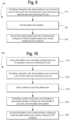
- Figure 9 is a flowchart of a method 900 for making a CNT yarn cable.
- the order of the steps in the method 900 is not constrained to that shown in Figure 9 or described in the following discussion. Several of the steps could occur in a different order without affecting the final result.
- step 910 controlling a deposition rate, plating is deposited so as to surround each of a pair of wires, each wire comprising one or more sub-cores, at least one sub-core comprising CNT yarn.
- Block 910 then transfers control to block 920.
- the plated wires are twisted together.
- the twisting step comprises twisting together a plurality of sub-cores, thereby creating the pair of twisted wires, each comprising the plurality of sub-cores.
- the twisting step comprises controlling a number of sub-cores.
- the twisting step comprises controlling an approximate diameter of at least one of the plurality of sub-cores. Block 920 then transfers control to block 930.
- step 930 the plated twisted wires are surrounded with an electrical layer configured to shield the plated twisted wires, thereby creating the CNT cable. Block 930 then terminates the process.
- the method includes an additional step, performed after the depositing step and prior to the surrounding step, of placing a dielectric around the plated twisted wires.
- the method includes an additional step, performed before the creating step, of chemically pretreating the CNT yarn cable.
- the pretreating step comprises chemically pretreating the CNT yarn cable by performing an acid wash using chlorosulfonic acid.
- depositing comprises depositing plating at a rate less than or equal to approximately 12 microns per minute.
- the pretreating step comprises treatment of the CNT yarn cable with a solvent.
- the solvent comprises one or more of acetone, isopropyl alcohol (IPA), and methanol.
- IPA isopropyl alcohol
- Figure 10 is a flowchart of a method 1000 for making a CNT yarn cable.
- the order of the steps in the method 1000 is not constrained to that shown in Figure 10 or described in the following discussion. Several of the steps could occur in a different order without affecting the final result.
- step 1010 using chlorosulfonic acid, at least one of a plurality of sub-cores comprising CNT yarn is chemically pretreated. Block 1010 then transfers control to block 1020.
- step 1020 controlling a deposition rate, plating is deposited so as to surround each of a pair of wires, each wire comprising a sub-core.
- Block 1020 then transfers control to block 1030.
- step 1030 a dielectric is placed around the plated twisted wires. Block 1030 then transfers control to block 1040.
- step 1040 controlling a number of sub-cores, and controlling an approximate diameter of at least one of the plurality of sub-cores, the plated wires are twisted together. Block 1040 then transfers control to block 1050.
- step 1050 the dielectric is surrounded with an electrical layer configured to shield the plated twisted wires, thereby creating the CNT cable. Block 1050 then terminates the process.
- Embodiments of the invention provide numerous benefits. Enhancements according to embodiments of the invention of the electroplating process, including one or more of controlling the deposition rate and pretreatment, achieves one or more of increasing wire conductivity and lowering total cable weight.
- Pretreatment with CSY according to embodiments of the invention results in an ideal, smooth substrate for electroplating the wire.
- a weight of an embodiment of the invention is approximately inversely proportional to signal frequency. Less plating is required for signal wires operating at higher frequencies according to embodiments of the invention.
- Embodiments of the invention provide skin depth confinement of RF signals.
- embodiments of the invention are more resilient to flexural, tension and other induced mechanical strain during installation, integration, testing, and operation.
- Plating thickness is optimized to match a natural skin depth of high-frequency signals, ensuring that signal quality is not substantially affected by use of a strong, lightweight CNT core instead of a prior art copper wire.
- Embodiments of the invention provide data transfer rates in a single twisted wire pair of at least approximately 1.25 Gigabits per second (Gbit/s), which is more than 40 times the maximum data rate of prior art cables lacking electroplated copper, which are limited to a maximum data rate of approximately 30 Mbit/s.
- the data transfer rate of at least approximately 1.25 Gbit/s is also more than three times the data transfer speed of Universal Serial Bus (USB) 2.0.
- USB Universal Serial Bus
Landscapes
- Chemical & Material Sciences (AREA)
- Engineering & Computer Science (AREA)
- Materials Engineering (AREA)
- Organic Chemistry (AREA)
- Chemical Kinetics & Catalysis (AREA)
- Electrochemistry (AREA)
- Metallurgy (AREA)
- Manufacturing & Machinery (AREA)
- Nanotechnology (AREA)
- Inorganic Chemistry (AREA)
- Non-Insulated Conductors (AREA)
- Ropes Or Cables (AREA)
- Carbon And Carbon Compounds (AREA)
- Yarns And Mechanical Finishing Of Yarns Or Ropes (AREA)
- Conductive Materials (AREA)
- Insulated Conductors (AREA)
- Electroplating Methods And Accessories (AREA)
- Processes Specially Adapted For Manufacturing Cables (AREA)
Claims (13)
- Kohlenstoffnanoröhrchen(CNT-)Kabel, umfassend:ein Paar plattierter verdrillter Drähte, wobei jeder Draht einen oder mehrere Unterkerne umfasst, wobei zumindest ein Unterkern CNT-Garn umfasst, wobei das CNT-Garn unter Verwendung von Chlorsulfonsäure chemisch vorbehandelt ist;ein Dielektrikum, das die plattierten verdrillten Drähte umgibt; undeine elektrische Schicht, die das Dielektrikum umgibt, wobei die elektrische Schicht das CNT-Kabel abschirmt.
- CNT-Kabel nach Anspruch 1, ferner umfassend ein Dielektrikum, das die Plattierung umgibt, wobei die elektrische Schicht das Dielektrikum umgibt.
- CNT-Kabel nach Anspruch 1, wobei die elektrische Schicht durch eine physische Schicht umgeben ist, die ein Geflecht umfasst, das konfiguriert ist, um die elektrische Schicht vor Abrieb zu schützen.
- CNT-Kabel nach Anspruch 1, wobei die Plattierung eines oder mehrere von Silber, Gold und Kupfer umfasst oder die Plattierung eine Dicke von weniger als oder gleich ungefähr 15 Mikron aufweist.
- CNT-Kabel nach Anspruch 1, wobei die Unterkerne miteinander verdrillt sind und wobei zumindest einer der Unterkerne chemisch gestrecktes CNT-Garn umfasst.
- CNT-Kabel nach Anspruch 1, wobei das CNT-Kabel einen Hochfrequenz(HF-)Einfügungsverlust von weniger als oder gleich ungefähr 2,0 Dezibel pro Fuß bei einer Frequenz von ungefähr 1 Gigahertz oder einen Hochfrequenz(HF-)Einfügungsverlust von weniger als oder gleich ungefähr 4,0 Dezibel pro Fuß bei einer Frequenz von ungefähr 4 Gigahertz aufweist oder das CNT-Kabel in der Lage ist, eine Datenübertragungsrate in einem einzelnen verdrillten Drahtpaar von zumindest ungefähr 1,25 Gigabit pro Sekunde (Gbit/s) bereitzustellen.
- CNT-Kabel nach Anspruch 1, wobei das CNT-Kabel Leitfähigkeit zwischen ungefähr 10 Megasiemens pro Meter und ungefähr 58,5 Megasiemens pro Meter aufweist.
- CNT-Kabel nach Anspruch 1, wobei das CNT-Kabel eine Reduzierung im Gewicht relativ zu Kupferdraht von der Stange von zwischen ungefähr 60 % und ungefähr 90 % bereitstellt.
- CNT-Kabel nach Anspruch 1, wobei das CNT-Kabel eine Korngröße von weniger als oder gleich ungefähr 10 Mikron aufweist.
- CNT-Kabel nach Anspruch 1, wobei das CNT-Kabel eines oder mehrere von einem Vierachsgarn und einem Triaxgarn umfasst.
- Verfahren zum Herstellen eines Kohlenstoffnanoröhrchen(CNT-)Kabels, umfassend:Abscheiden von Plattierung unter Verwendung einer gesteuerten Abscheidungsrate, um jeden von einem Paar von Drähten zu umgeben, wobei jeder Draht einen oder mehrere Unterkerne umfasst, wobei zumindest ein Unterkern CNT-Garn umfasst;chemisches Vorbehandeln des CNT-Garns unter Verwendung von Chlorsulfonsäure;Verdrillen der plattierten Drähte miteinander; undUmgeben der plattierten verdrillten Drähte mit einer elektrischen Schicht, welche die plattierten verdrillten Drähte abschirmt, wodurch das CNT-Kabel erzeugt wird.
- Verfahren nach Anspruch 11, ferner umfassend einen Schritt, der nach dem Abscheidungsschritt und vor dem Umgebungsschritt durchgeführt wird, des Platzierens eines Dielektrikums um die plattierten verdrillten Drähte.
- Verfahren nach Anspruch 11, wobei der Abscheidungsschritt Abscheiden von Plattierung umfassend eines oder mehrere von Silber, Gold und Kupfer und mit einer Rate von weniger als oder gleich ungefähr 12 Mikron pro Minute umfasst.
Applications Claiming Priority (2)
| Application Number | Priority Date | Filing Date | Title |
|---|---|---|---|
| US15/791,730 US10128022B1 (en) | 2017-10-24 | 2017-10-24 | Lightweight carbon nanotube cable comprising a pair of plated twisted wires |
| PCT/US2018/052604 WO2019083665A1 (en) | 2017-10-24 | 2018-09-25 | LIGHT CARBON NANOTUBE CABLE COMPRISING A PAIR OF PLATED TWISTED YARNS |
Publications (2)
| Publication Number | Publication Date |
|---|---|
| EP3701548A1 EP3701548A1 (de) | 2020-09-02 |
| EP3701548B1 true EP3701548B1 (de) | 2025-04-16 |
Family
ID=63915108
Family Applications (1)
| Application Number | Title | Priority Date | Filing Date |
|---|---|---|---|
| EP18789534.7A Active EP3701548B1 (de) | 2017-10-24 | 2018-09-25 | Leichtes kohlenstoffnanoröhrchenkabel mit einem paar plattierter verdrillter drähte |
Country Status (4)
| Country | Link |
|---|---|
| US (2) | US10128022B1 (de) |
| EP (1) | EP3701548B1 (de) |
| JP (2) | JP2021501437A (de) |
| WO (1) | WO2019083665A1 (de) |
Families Citing this family (4)
| Publication number | Priority date | Publication date | Assignee | Title |
|---|---|---|---|---|
| US11424048B2 (en) * | 2018-06-28 | 2022-08-23 | Carlisle Interconnect Technologies, Inc. | Coaxial cable utilizing plated carbon nanotube elements and method of manufacturing same |
| US10892070B2 (en) * | 2019-02-01 | 2021-01-12 | Baker Hughes Oilfield Operations, Llc | Methods of treating carbon nanotubes and conductive elements including such carbon nanotubes |
| CN114477147B (zh) * | 2022-03-02 | 2023-05-16 | 中国科学院苏州纳米技术与纳米仿生研究所 | 一种提高碳纳米管纤维致密化程度的后处理方法 |
| JP2023146731A (ja) * | 2022-03-29 | 2023-10-12 | 国立研究開発法人日本原子力研究開発機構 | 複合糸、複合糸の製造方法、及び複合シート |
Family Cites Families (40)
| Publication number | Priority date | Publication date | Assignee | Title |
|---|---|---|---|---|
| JP2005277096A (ja) * | 2004-03-24 | 2005-10-06 | Japan Science & Technology Agency | カーボンナノチューブ含有金属膜を用いてなる半導体配線とその製造方法、およびカーボンナノチューブ含有金属膜の製造方法 |
| DE102004041701A1 (de) * | 2004-08-28 | 2006-03-02 | Enthone Inc., West Haven | Verfahren zur elektrolytischen Abscheidung von Metallen |
| CN101086939B (zh) * | 2006-06-09 | 2010-05-12 | 清华大学 | 场发射元件及其制备方法 |
| CN101286384B (zh) * | 2007-04-11 | 2010-12-29 | 清华大学 | 电磁屏蔽线缆 |
| CN105244071B (zh) * | 2008-02-01 | 2018-11-30 | 北京富纳特创新科技有限公司 | 线缆 |
| CN101556839B (zh) * | 2008-04-09 | 2011-08-24 | 清华大学 | 线缆 |
| DE102008013518A1 (de) * | 2008-03-07 | 2009-09-17 | Siemens Aktiengesellschaft | Strangförmiger Materialverbund mit CNT-Garnen und Verfahren zu desssen Herstellung |
| TWI345792B (en) * | 2008-03-07 | 2011-07-21 | Hon Hai Prec Ind Co Ltd | Cable |
| ES2753901T3 (es) * | 2008-05-07 | 2020-04-14 | Nanocomp Technologies Inc | Mazo de cables y cables eléctricos coaxiales basados en nanotubos de carbón |
| JP2010114019A (ja) | 2008-11-10 | 2010-05-20 | Hitachi Cable Ltd | ケーブル |
| US8354593B2 (en) * | 2009-07-10 | 2013-01-15 | Nanocomp Technologies, Inc. | Hybrid conductors and method of making same |
| US8246860B2 (en) * | 2009-10-23 | 2012-08-21 | Tsinghua University | Carbon nanotube composite, method for making the same, and electrochemical capacitor using the same |
| JP2014508370A (ja) * | 2010-09-23 | 2014-04-03 | アプライド ナノストラクチャード ソリューションズ リミテッド ライアビリティー カンパニー | 強化送電線のセルフシールドワイヤとしてのcnt浸出繊維 |
| US9233492B2 (en) * | 2010-10-12 | 2016-01-12 | Florida State University Research Foundation, Inc. | Composite materials reinforced with carbon nanotube yarns |
| WO2012065107A1 (en) * | 2010-11-12 | 2012-05-18 | Nanocomp Technologies, Inc. | Systems and methods for thermal management of electronic components |
| WO2012082714A2 (en) * | 2010-12-14 | 2012-06-21 | Atkins & Pearce, Inc. | Braided carbon nanotube threads and methods of manufacturing the same |
| US8853540B2 (en) * | 2011-04-19 | 2014-10-07 | Commscope, Inc. Of North Carolina | Carbon nanotube enhanced conductors for communications cables and related communications cables and methods |
| GB201116670D0 (en) * | 2011-09-27 | 2011-11-09 | Cambridge Entpr Ltd | Materials and methods for insulation of conducting fibres, and insulated products |
| US20130102195A1 (en) * | 2011-10-24 | 2013-04-25 | Alan L. Pocrass | Multiport RJ Stack Connector With Interlocking Mechanism to Attach to Additional Multiport Stack |
| US8808792B2 (en) * | 2012-01-17 | 2014-08-19 | Northrop Grumman Systems Corporation | Carbon nanotube conductor with enhanced electrical conductivity |
| JP2015523944A (ja) * | 2012-04-09 | 2015-08-20 | ナノコンプ テクノロジーズ,インク. | 導電性を増加させるために導電性堆積物を有しているナノチューブ材料 |
| WO2013170021A1 (en) * | 2012-05-11 | 2013-11-14 | General Cable Technologies Corporation | Light weight braid for cable shielding applications |
| US20140102755A1 (en) * | 2012-10-17 | 2014-04-17 | Commscope, Inc. Of North Carolina | Communications Cables Having Electrically Insulative but Thermally Conductive Cable Jackets |
| US9293233B2 (en) * | 2013-02-11 | 2016-03-22 | Tyco Electronics Corporation | Composite cable |
| CN103377764A (zh) * | 2013-07-02 | 2013-10-30 | 晶锋集团股份有限公司 | 一种通信传输电缆 |
| MX373439B (es) * | 2013-07-19 | 2020-05-20 | Dow Global Technologies Llc | Cable con nucleo compuesto de polimero. |
| CN204146387U (zh) * | 2014-04-23 | 2015-02-11 | 北京富纳特创新科技有限公司 | 防辐射防静电面料及防辐射防静电服装 |
| CN105097065B (zh) * | 2014-04-23 | 2018-03-02 | 北京富纳特创新科技有限公司 | 碳纳米管复合导线 |
| CN104021837B (zh) * | 2014-05-31 | 2017-12-26 | 西安交通大学 | 一种非金属轻型导电线及其方法和应用产品 |
| US10032542B2 (en) * | 2014-11-07 | 2018-07-24 | Cable Components Group, Llc | Compositions for compounding, extrusion and melt processing of foamable and cellular halogen-free polymers |
| WO2016086166A1 (en) * | 2014-11-26 | 2016-06-02 | Nanocomp Technologies, Inc. | Hierarchically structured carbon nanotube articles and methods for production thereof |
| WO2016126818A1 (en) * | 2015-02-03 | 2016-08-11 | Nanocomp Technologies, Inc. | Carbon nanotube structures and methods for production thereof |
| DE102015221906A1 (de) * | 2015-11-06 | 2017-05-11 | Leoni Kabel Holding Gmbh | Datenkabel sowie Verwendung des Datenkabels in einem Kraftfahrzeug |
| US9972420B2 (en) * | 2015-12-08 | 2018-05-15 | The Boeing Company | Carbon nanotube shielding for transmission cables |
| GB201602653D0 (en) * | 2016-02-15 | 2016-03-30 | Grant Duncan A | An arrangement for the electro-deposition of metal on carbon nanotube fibre |
| US10016766B2 (en) * | 2016-03-24 | 2018-07-10 | The Boeing Company | Dust mitigation system utilizing conductive fibers |
| US10109391B2 (en) * | 2017-02-20 | 2018-10-23 | Delphi Technologies, Inc. | Metallic/carbon nanotube composite wire |
| US10115492B2 (en) * | 2017-02-24 | 2018-10-30 | Delphi Technologies, Inc. | Electrically conductive carbon nanotube wire having a metallic coating and methods of forming same |
| US20180315521A1 (en) * | 2017-05-01 | 2018-11-01 | Minnesota Wire, Inc. | Carbon nanotube based cabling |
| CN107068254A (zh) | 2017-06-09 | 2017-08-18 | 安徽埃克森科技集团有限公司 | 一种用于航空航天的超轻型电缆 |
-
2017
- 2017-10-24 US US15/791,730 patent/US10128022B1/en active Active
-
2018
- 2018-09-25 WO PCT/US2018/052604 patent/WO2019083665A1/en not_active Ceased
- 2018-09-25 US US16/140,811 patent/US11875921B2/en active Active
- 2018-09-25 JP JP2020521595A patent/JP2021501437A/ja active Pending
- 2018-09-25 EP EP18789534.7A patent/EP3701548B1/de active Active
-
2023
- 2023-04-12 JP JP2023065053A patent/JP2023095866A/ja active Pending
Also Published As
| Publication number | Publication date |
|---|---|
| EP3701548A1 (de) | 2020-09-02 |
| WO2019083665A1 (en) | 2019-05-02 |
| JP2021501437A (ja) | 2021-01-14 |
| US10128022B1 (en) | 2018-11-13 |
| JP2023095866A (ja) | 2023-07-06 |
| US11875921B2 (en) | 2024-01-16 |
| US20190122788A1 (en) | 2019-04-25 |
Similar Documents
| Publication | Publication Date | Title |
|---|---|---|
| US11875921B2 (en) | Lightweight carbon nanotube cable comprising a pair of plated twisted wires | |
| CN112164485A (zh) | 一种高速高频信号传输铜导体电缆的生产工艺 | |
| CN203366796U (zh) | 一种低损耗同轴电缆 | |
| CN112652426A (zh) | 一种高速机车线缆的制备工艺 | |
| CN110277196B (zh) | 一种超高速数据传输电缆及其制造工艺 | |
| CN221708440U (zh) | 一种移动医疗设备电缆 | |
| CN203242432U (zh) | 多对平行对称轴电缆 | |
| KR102207956B1 (ko) | 고차폐성 및 고절연성을 갖는 오디오케이블 제작 방법 및 이에 의해 제작된 오디오케이블 | |
| CN118969362A (zh) | 一种高柔耐扭机器人电缆铜导体及其制备方法 | |
| CN106128567A (zh) | 一种耐高温抗辐射电线及其制备方法 | |
| WO2020172281A1 (en) | Wire with elongated cross section for conductor shielding field and background of the invention | |
| JP2007250235A (ja) | 同軸ケーブル用中空コア体,同コア体の製造方法,同コア体を用いる同軸ケーブル | |
| CN101393785B (zh) | 编织型同轴通讯电缆 | |
| CN204760128U (zh) | 低损耗半柔同轴电缆 | |
| WO2000074080A1 (en) | An article shielded against emi and rfi | |
| CN211208039U (zh) | 一种八类线 | |
| CN111799030B (zh) | 高频无峰值屏蔽电缆及其制作方法 | |
| CN201466190U (zh) | 低损耗半柔射频同轴电缆 | |
| CN222394594U (zh) | 一种石墨烯屏蔽vr数据线 | |
| CN206293208U (zh) | 一种多芯极细同轴电缆 | |
| CN211150175U (zh) | 一种轻型半柔同轴电缆 | |
| CN217134075U (zh) | 一种稳相同轴电缆 | |
| CN111755165A (zh) | 免电磁干扰线缆导体 | |
| CN215417563U (zh) | Pbo高频应用传输电缆 | |
| CN219997888U (zh) | 一种极细的并排电缆 |
Legal Events
| Date | Code | Title | Description |
|---|---|---|---|
| STAA | Information on the status of an ep patent application or granted ep patent |
Free format text: STATUS: UNKNOWN |
|
| STAA | Information on the status of an ep patent application or granted ep patent |
Free format text: STATUS: THE INTERNATIONAL PUBLICATION HAS BEEN MADE |
|
| PUAI | Public reference made under article 153(3) epc to a published international application that has entered the european phase |
Free format text: ORIGINAL CODE: 0009012 |
|
| STAA | Information on the status of an ep patent application or granted ep patent |
Free format text: STATUS: REQUEST FOR EXAMINATION WAS MADE |
|
| 17P | Request for examination filed |
Effective date: 20200306 |
|
| AK | Designated contracting states |
Kind code of ref document: A1 Designated state(s): AL AT BE BG CH CY CZ DE DK EE ES FI FR GB GR HR HU IE IS IT LI LT LU LV MC MK MT NL NO PL PT RO RS SE SI SK SM TR |
|
| AX | Request for extension of the european patent |
Extension state: BA ME |
|
| DAV | Request for validation of the european patent (deleted) | ||
| DAX | Request for extension of the european patent (deleted) | ||
| P01 | Opt-out of the competence of the unified patent court (upc) registered |
Effective date: 20230607 |
|
| STAA | Information on the status of an ep patent application or granted ep patent |
Free format text: STATUS: EXAMINATION IS IN PROGRESS |
|
| 17Q | First examination report despatched |
Effective date: 20230928 |
|
| GRAP | Despatch of communication of intention to grant a patent |
Free format text: ORIGINAL CODE: EPIDOSNIGR1 |
|
| STAA | Information on the status of an ep patent application or granted ep patent |
Free format text: STATUS: GRANT OF PATENT IS INTENDED |
|
| RIC1 | Information provided on ipc code assigned before grant |
Ipc: H01B 11/20 20060101ALI20240930BHEP Ipc: H01B 11/00 20060101ALI20240930BHEP Ipc: C25D 5/54 20060101ALI20240930BHEP Ipc: C25D 7/06 20060101ALI20240930BHEP Ipc: H01B 1/04 20060101AFI20240930BHEP |
|
| INTG | Intention to grant announced |
Effective date: 20241106 |
|
| GRAS | Grant fee paid |
Free format text: ORIGINAL CODE: EPIDOSNIGR3 |
|
| GRAA | (expected) grant |
Free format text: ORIGINAL CODE: 0009210 |
|
| STAA | Information on the status of an ep patent application or granted ep patent |
Free format text: STATUS: THE PATENT HAS BEEN GRANTED |
|
| AK | Designated contracting states |
Kind code of ref document: B1 Designated state(s): AL AT BE BG CH CY CZ DE DK EE ES FI FR GB GR HR HU IE IS IT LI LT LU LV MC MK MT NL NO PL PT RO RS SE SI SK SM TR |
|
| REG | Reference to a national code |
Ref country code: GB Ref legal event code: FG4D |
|
| REG | Reference to a national code |
Ref country code: CH Ref legal event code: EP Ref country code: DE Ref legal event code: R096 Ref document number: 602018081152 Country of ref document: DE |
|
| REG | Reference to a national code |
Ref country code: IE Ref legal event code: FG4D |
|
| REG | Reference to a national code |
Ref country code: NL Ref legal event code: MP Effective date: 20250416 |
|
| PG25 | Lapsed in a contracting state [announced via postgrant information from national office to epo] |
Ref country code: NL Free format text: LAPSE BECAUSE OF FAILURE TO SUBMIT A TRANSLATION OF THE DESCRIPTION OR TO PAY THE FEE WITHIN THE PRESCRIBED TIME-LIMIT Effective date: 20250416 |
|
| REG | Reference to a national code |
Ref country code: AT Ref legal event code: MK05 Ref document number: 1786360 Country of ref document: AT Kind code of ref document: T Effective date: 20250416 |
|
| PG25 | Lapsed in a contracting state [announced via postgrant information from national office to epo] |
Ref country code: FI Free format text: LAPSE BECAUSE OF FAILURE TO SUBMIT A TRANSLATION OF THE DESCRIPTION OR TO PAY THE FEE WITHIN THE PRESCRIBED TIME-LIMIT Effective date: 20250416 Ref country code: ES Free format text: LAPSE BECAUSE OF FAILURE TO SUBMIT A TRANSLATION OF THE DESCRIPTION OR TO PAY THE FEE WITHIN THE PRESCRIBED TIME-LIMIT Effective date: 20250416 Ref country code: PT Free format text: LAPSE BECAUSE OF FAILURE TO SUBMIT A TRANSLATION OF THE DESCRIPTION OR TO PAY THE FEE WITHIN THE PRESCRIBED TIME-LIMIT Effective date: 20250818 |
|
| PGFP | Annual fee paid to national office [announced via postgrant information from national office to epo] |
Ref country code: DE Payment date: 20250919 Year of fee payment: 8 |
|
| REG | Reference to a national code |
Ref country code: LT Ref legal event code: MG9D |
|
| PG25 | Lapsed in a contracting state [announced via postgrant information from national office to epo] |
Ref country code: NO Free format text: LAPSE BECAUSE OF FAILURE TO SUBMIT A TRANSLATION OF THE DESCRIPTION OR TO PAY THE FEE WITHIN THE PRESCRIBED TIME-LIMIT Effective date: 20250716 Ref country code: GR Free format text: LAPSE BECAUSE OF FAILURE TO SUBMIT A TRANSLATION OF THE DESCRIPTION OR TO PAY THE FEE WITHIN THE PRESCRIBED TIME-LIMIT Effective date: 20250717 |
|
| PG25 | Lapsed in a contracting state [announced via postgrant information from national office to epo] |
Ref country code: PL Free format text: LAPSE BECAUSE OF FAILURE TO SUBMIT A TRANSLATION OF THE DESCRIPTION OR TO PAY THE FEE WITHIN THE PRESCRIBED TIME-LIMIT Effective date: 20250416 |
|
| PG25 | Lapsed in a contracting state [announced via postgrant information from national office to epo] |
Ref country code: BG Free format text: LAPSE BECAUSE OF FAILURE TO SUBMIT A TRANSLATION OF THE DESCRIPTION OR TO PAY THE FEE WITHIN THE PRESCRIBED TIME-LIMIT Effective date: 20250416 |
|
| PGFP | Annual fee paid to national office [announced via postgrant information from national office to epo] |
Ref country code: GB Payment date: 20250919 Year of fee payment: 8 |
|
| PG25 | Lapsed in a contracting state [announced via postgrant information from national office to epo] |
Ref country code: HR Free format text: LAPSE BECAUSE OF FAILURE TO SUBMIT A TRANSLATION OF THE DESCRIPTION OR TO PAY THE FEE WITHIN THE PRESCRIBED TIME-LIMIT Effective date: 20250416 |
|
| PG25 | Lapsed in a contracting state [announced via postgrant information from national office to epo] |
Ref country code: AT Free format text: LAPSE BECAUSE OF FAILURE TO SUBMIT A TRANSLATION OF THE DESCRIPTION OR TO PAY THE FEE WITHIN THE PRESCRIBED TIME-LIMIT Effective date: 20250416 |
|
| PGFP | Annual fee paid to national office [announced via postgrant information from national office to epo] |
Ref country code: FR Payment date: 20250922 Year of fee payment: 8 |
|
| PG25 | Lapsed in a contracting state [announced via postgrant information from national office to epo] |
Ref country code: RS Free format text: LAPSE BECAUSE OF FAILURE TO SUBMIT A TRANSLATION OF THE DESCRIPTION OR TO PAY THE FEE WITHIN THE PRESCRIBED TIME-LIMIT Effective date: 20250716 |
|
| PG25 | Lapsed in a contracting state [announced via postgrant information from national office to epo] |
Ref country code: IS Free format text: LAPSE BECAUSE OF FAILURE TO SUBMIT A TRANSLATION OF THE DESCRIPTION OR TO PAY THE FEE WITHIN THE PRESCRIBED TIME-LIMIT Effective date: 20250816 |
|
| PG25 | Lapsed in a contracting state [announced via postgrant information from national office to epo] |
Ref country code: LV Free format text: LAPSE BECAUSE OF FAILURE TO SUBMIT A TRANSLATION OF THE DESCRIPTION OR TO PAY THE FEE WITHIN THE PRESCRIBED TIME-LIMIT Effective date: 20250416 |
|
| PG25 | Lapsed in a contracting state [announced via postgrant information from national office to epo] |
Ref country code: DK Free format text: LAPSE BECAUSE OF FAILURE TO SUBMIT A TRANSLATION OF THE DESCRIPTION OR TO PAY THE FEE WITHIN THE PRESCRIBED TIME-LIMIT Effective date: 20250416 Ref country code: SM Free format text: LAPSE BECAUSE OF FAILURE TO SUBMIT A TRANSLATION OF THE DESCRIPTION OR TO PAY THE FEE WITHIN THE PRESCRIBED TIME-LIMIT Effective date: 20250416 |
|
| REG | Reference to a national code |
Ref country code: DE Ref legal event code: R097 Ref document number: 602018081152 Country of ref document: DE |
|
| PG25 | Lapsed in a contracting state [announced via postgrant information from national office to epo] |
Ref country code: CZ Free format text: LAPSE BECAUSE OF FAILURE TO SUBMIT A TRANSLATION OF THE DESCRIPTION OR TO PAY THE FEE WITHIN THE PRESCRIBED TIME-LIMIT Effective date: 20250416 |
|
| PG25 | Lapsed in a contracting state [announced via postgrant information from national office to epo] |
Ref country code: EE Free format text: LAPSE BECAUSE OF FAILURE TO SUBMIT A TRANSLATION OF THE DESCRIPTION OR TO PAY THE FEE WITHIN THE PRESCRIBED TIME-LIMIT Effective date: 20250416 |
|
| PG25 | Lapsed in a contracting state [announced via postgrant information from national office to epo] |
Ref country code: SK Free format text: LAPSE BECAUSE OF FAILURE TO SUBMIT A TRANSLATION OF THE DESCRIPTION OR TO PAY THE FEE WITHIN THE PRESCRIBED TIME-LIMIT Effective date: 20250416 Ref country code: RO Free format text: LAPSE BECAUSE OF FAILURE TO SUBMIT A TRANSLATION OF THE DESCRIPTION OR TO PAY THE FEE WITHIN THE PRESCRIBED TIME-LIMIT Effective date: 20250416 |
|
| PG25 | Lapsed in a contracting state [announced via postgrant information from national office to epo] |
Ref country code: IT Free format text: LAPSE BECAUSE OF FAILURE TO SUBMIT A TRANSLATION OF THE DESCRIPTION OR TO PAY THE FEE WITHIN THE PRESCRIBED TIME-LIMIT Effective date: 20250416 |
|
| PLBE | No opposition filed within time limit |
Free format text: ORIGINAL CODE: 0009261 |
|
| STAA | Information on the status of an ep patent application or granted ep patent |
Free format text: STATUS: NO OPPOSITION FILED WITHIN TIME LIMIT |
|
| REG | Reference to a national code |
Ref country code: CH Ref legal event code: L10 Free format text: ST27 STATUS EVENT CODE: U-0-0-L10-L00 (AS PROVIDED BY THE NATIONAL OFFICE) Effective date: 20260225 |
|
| 26N | No opposition filed |
Effective date: 20260119 |
|
| REG | Reference to a national code |
Ref country code: CH Ref legal event code: H13 Free format text: ST27 STATUS EVENT CODE: U-0-0-H10-H13 (AS PROVIDED BY THE NATIONAL OFFICE) Effective date: 20260504 |