EP3701516B1 - Breitbandige adaptive linsenanordnung für anzeige von erweiterter realität - Google Patents
Breitbandige adaptive linsenanordnung für anzeige von erweiterter realität Download PDFInfo
- Publication number
- EP3701516B1 EP3701516B1 EP18871789.6A EP18871789A EP3701516B1 EP 3701516 B1 EP3701516 B1 EP 3701516B1 EP 18871789 A EP18871789 A EP 18871789A EP 3701516 B1 EP3701516 B1 EP 3701516B1
- Authority
- EP
- European Patent Office
- Prior art keywords
- waveplate
- light
- switchable
- lens
- broadband
- Prior art date
- Legal status (The legal status is an assumption and is not a legal conclusion. Google has not performed a legal analysis and makes no representation as to the accuracy of the status listed.)
- Active
Links
Images


Classifications
-
- G—PHYSICS
- G02—OPTICS
- G02B—OPTICAL ELEMENTS, SYSTEMS OR APPARATUS
- G02B1/00—Optical elements characterised by the material of which they are made; Optical coatings for optical elements
-
- G—PHYSICS
- G02—OPTICS
- G02B—OPTICAL ELEMENTS, SYSTEMS OR APPARATUS
- G02B27/00—Optical systems or apparatus not provided for by any of the groups G02B1/00 - G02B26/00, G02B30/00
- G02B27/01—Head-up displays
- G02B27/017—Head mounted
- G02B27/0172—Head mounted characterised by optical features
-
- G—PHYSICS
- G02—OPTICS
- G02B—OPTICAL ELEMENTS, SYSTEMS OR APPARATUS
- G02B5/00—Optical elements other than lenses
- G02B5/18—Diffraction gratings
- G02B5/1833—Diffraction gratings comprising birefringent materials
-
- G—PHYSICS
- G02—OPTICS
- G02B—OPTICAL ELEMENTS, SYSTEMS OR APPARATUS
- G02B5/00—Optical elements other than lenses
- G02B5/30—Polarising elements
-
- G—PHYSICS
- G02—OPTICS
- G02B—OPTICAL ELEMENTS, SYSTEMS OR APPARATUS
- G02B5/00—Optical elements other than lenses
- G02B5/30—Polarising elements
- G02B5/3016—Polarising elements involving passive liquid crystal elements
-
- G—PHYSICS
- G02—OPTICS
- G02B—OPTICAL ELEMENTS, SYSTEMS OR APPARATUS
- G02B6/00—Light guides; Structural details of arrangements comprising light guides and other optical elements, e.g. couplings
- G02B6/10—Light guides; Structural details of arrangements comprising light guides and other optical elements, e.g. couplings of the optical waveguide type
- G02B6/12—Light guides; Structural details of arrangements comprising light guides and other optical elements, e.g. couplings of the optical waveguide type of the integrated circuit kind
- G02B6/122—Basic optical elements, e.g. light-guiding paths
-
- G—PHYSICS
- G02—OPTICS
- G02B—OPTICAL ELEMENTS, SYSTEMS OR APPARATUS
- G02B6/00—Light guides; Structural details of arrangements comprising light guides and other optical elements, e.g. couplings
- G02B6/24—Coupling light guides
- G02B6/26—Optical coupling means
- G02B6/34—Optical coupling means utilising prism or grating
-
- G—PHYSICS
- G02—OPTICS
- G02F—OPTICAL DEVICES OR ARRANGEMENTS FOR THE CONTROL OF LIGHT BY MODIFICATION OF THE OPTICAL PROPERTIES OF THE MEDIA OF THE ELEMENTS INVOLVED THEREIN; NON-LINEAR OPTICS; FREQUENCY-CHANGING OF LIGHT; OPTICAL LOGIC ELEMENTS; OPTICAL ANALOGUE/DIGITAL CONVERTERS
- G02F1/00—Devices or arrangements for the control of the intensity, colour, phase, polarisation or direction of light arriving from an independent light source, e.g. switching, gating or modulating; Non-linear optics
- G02F1/01—Devices or arrangements for the control of the intensity, colour, phase, polarisation or direction of light arriving from an independent light source, e.g. switching, gating or modulating; Non-linear optics for the control of the intensity, phase, polarisation or colour
- G02F1/13—Devices or arrangements for the control of the intensity, colour, phase, polarisation or direction of light arriving from an independent light source, e.g. switching, gating or modulating; Non-linear optics for the control of the intensity, phase, polarisation or colour based on liquid crystals, e.g. single liquid crystal display cells
- G02F1/133—Constructional arrangements; Operation of liquid crystal cells; Circuit arrangements
- G02F1/1333—Constructional arrangements; Manufacturing methods
- G02F1/1335—Structural association of cells with optical devices, e.g. polarisers or reflectors
- G02F1/133526—Lenses, e.g. microlenses or Fresnel lenses
-
- G—PHYSICS
- G02—OPTICS
- G02F—OPTICAL DEVICES OR ARRANGEMENTS FOR THE CONTROL OF LIGHT BY MODIFICATION OF THE OPTICAL PROPERTIES OF THE MEDIA OF THE ELEMENTS INVOLVED THEREIN; NON-LINEAR OPTICS; FREQUENCY-CHANGING OF LIGHT; OPTICAL LOGIC ELEMENTS; OPTICAL ANALOGUE/DIGITAL CONVERTERS
- G02F1/00—Devices or arrangements for the control of the intensity, colour, phase, polarisation or direction of light arriving from an independent light source, e.g. switching, gating or modulating; Non-linear optics
- G02F1/01—Devices or arrangements for the control of the intensity, colour, phase, polarisation or direction of light arriving from an independent light source, e.g. switching, gating or modulating; Non-linear optics for the control of the intensity, phase, polarisation or colour
- G02F1/13—Devices or arrangements for the control of the intensity, colour, phase, polarisation or direction of light arriving from an independent light source, e.g. switching, gating or modulating; Non-linear optics for the control of the intensity, phase, polarisation or colour based on liquid crystals, e.g. single liquid crystal display cells
- G02F1/133—Constructional arrangements; Operation of liquid crystal cells; Circuit arrangements
- G02F1/1333—Constructional arrangements; Manufacturing methods
- G02F1/1335—Structural association of cells with optical devices, e.g. polarisers or reflectors
- G02F1/133528—Polarisers
-
- G—PHYSICS
- G02—OPTICS
- G02F—OPTICAL DEVICES OR ARRANGEMENTS FOR THE CONTROL OF LIGHT BY MODIFICATION OF THE OPTICAL PROPERTIES OF THE MEDIA OF THE ELEMENTS INVOLVED THEREIN; NON-LINEAR OPTICS; FREQUENCY-CHANGING OF LIGHT; OPTICAL LOGIC ELEMENTS; OPTICAL ANALOGUE/DIGITAL CONVERTERS
- G02F1/00—Devices or arrangements for the control of the intensity, colour, phase, polarisation or direction of light arriving from an independent light source, e.g. switching, gating or modulating; Non-linear optics
- G02F1/01—Devices or arrangements for the control of the intensity, colour, phase, polarisation or direction of light arriving from an independent light source, e.g. switching, gating or modulating; Non-linear optics for the control of the intensity, phase, polarisation or colour
- G02F1/13—Devices or arrangements for the control of the intensity, colour, phase, polarisation or direction of light arriving from an independent light source, e.g. switching, gating or modulating; Non-linear optics for the control of the intensity, phase, polarisation or colour based on liquid crystals, e.g. single liquid crystal display cells
- G02F1/133—Constructional arrangements; Operation of liquid crystal cells; Circuit arrangements
- G02F1/1333—Constructional arrangements; Manufacturing methods
- G02F1/1337—Surface-induced orientation of the liquid crystal molecules, e.g. by alignment layers
-
- G—PHYSICS
- G06—COMPUTING OR CALCULATING; COUNTING
- G06T—IMAGE DATA PROCESSING OR GENERATION, IN GENERAL
- G06T19/00—Manipulating 3D models or images for computer graphics
- G06T19/006—Mixed reality
-
- G—PHYSICS
- G06—COMPUTING OR CALCULATING; COUNTING
- G06V—IMAGE OR VIDEO RECOGNITION OR UNDERSTANDING
- G06V20/00—Scenes; Scene-specific elements
- G06V20/20—Scenes; Scene-specific elements in augmented reality scenes
-
- G—PHYSICS
- G09—EDUCATION; CRYPTOGRAPHY; DISPLAY; ADVERTISING; SEALS
- G09G—ARRANGEMENTS OR CIRCUITS FOR CONTROL OF INDICATING DEVICES USING STATIC MEANS TO PRESENT VARIABLE INFORMATION
- G09G3/00—Control arrangements or circuits, of interest only in connection with visual indicators other than cathode-ray tubes
- G09G3/001—Control arrangements or circuits, of interest only in connection with visual indicators other than cathode-ray tubes using specific devices not provided for in groups G09G3/02 - G09G3/36, e.g. using an intermediate record carrier such as a film slide; Projection systems; Display of non-alphanumerical information, solely or in combination with alphanumerical information, e.g. digital display on projected diapositive as background
- G09G3/002—Control arrangements or circuits, of interest only in connection with visual indicators other than cathode-ray tubes using specific devices not provided for in groups G09G3/02 - G09G3/36, e.g. using an intermediate record carrier such as a film slide; Projection systems; Display of non-alphanumerical information, solely or in combination with alphanumerical information, e.g. digital display on projected diapositive as background to project the image of a two-dimensional display, such as an array of light emitting or modulating elements or a CRT
-
- G—PHYSICS
- G09—EDUCATION; CRYPTOGRAPHY; DISPLAY; ADVERTISING; SEALS
- G09G—ARRANGEMENTS OR CIRCUITS FOR CONTROL OF INDICATING DEVICES USING STATIC MEANS TO PRESENT VARIABLE INFORMATION
- G09G3/00—Control arrangements or circuits, of interest only in connection with visual indicators other than cathode-ray tubes
- G09G3/001—Control arrangements or circuits, of interest only in connection with visual indicators other than cathode-ray tubes using specific devices not provided for in groups G09G3/02 - G09G3/36, e.g. using an intermediate record carrier such as a film slide; Projection systems; Display of non-alphanumerical information, solely or in combination with alphanumerical information, e.g. digital display on projected diapositive as background
- G09G3/003—Control arrangements or circuits, of interest only in connection with visual indicators other than cathode-ray tubes using specific devices not provided for in groups G09G3/02 - G09G3/36, e.g. using an intermediate record carrier such as a film slide; Projection systems; Display of non-alphanumerical information, solely or in combination with alphanumerical information, e.g. digital display on projected diapositive as background to produce spatial visual effects
-
- G—PHYSICS
- G09—EDUCATION; CRYPTOGRAPHY; DISPLAY; ADVERTISING; SEALS
- G09G—ARRANGEMENTS OR CIRCUITS FOR CONTROL OF INDICATING DEVICES USING STATIC MEANS TO PRESENT VARIABLE INFORMATION
- G09G5/00—Control arrangements or circuits for visual indicators common to cathode-ray tube indicators and other visual indicators
- G09G5/14—Display of multiple viewports
-
- G—PHYSICS
- G02—OPTICS
- G02B—OPTICAL ELEMENTS, SYSTEMS OR APPARATUS
- G02B27/00—Optical systems or apparatus not provided for by any of the groups G02B1/00 - G02B26/00, G02B30/00
- G02B27/01—Head-up displays
- G02B27/0101—Head-up displays characterised by optical features
- G02B2027/0127—Head-up displays characterised by optical features comprising devices increasing the depth of field
-
- G—PHYSICS
- G02—OPTICS
- G02B—OPTICAL ELEMENTS, SYSTEMS OR APPARATUS
- G02B27/00—Optical systems or apparatus not provided for by any of the groups G02B1/00 - G02B26/00, G02B30/00
- G02B27/01—Head-up displays
- G02B27/0179—Display position adjusting means not related to the information to be displayed
- G02B2027/0185—Displaying image at variable distance
Definitions
- the present disclosure relates to display systems and, more particularly, to augmented and virtual reality display systems.
- a virtual reality, or "VR”, scenario typically involves presentation of digital or virtual image information without transparency to other actual real-world visual input;
- an augmented reality, or "AR”, scenario typically involves presentation of digital or virtual image information as an augmentation to visualization of the actual world around the user.
- a mixed reality, or "MR”, scenario is a type of AR scenario and typically involves virtual objects that are integrated into, and responsive to, the natural world. For example, in an MR scenario, AR image content may be blocked by or otherwise be perceived as interacting with objects in the real world.
- the third up waveguide 290 passes its output light through both the first 350 and second 340 lenses before reaching the eye 210; the combined optical power of the first 350 and second 340 lenses may be configured to create another incremental amount of wavefront curvature so that the eye/brain interprets light coming from the third waveguide 290 as coming from a second focal plane that is even closer inward toward the person from optical infinity than was light from the next waveguide up 280.
- the exit beams 650 are illustrated as substantially parallel but, as discussed herein, they may also be redirected to propagate to the eye 210 at an angle (e.g., forming divergent exit beams), depending on the depth plane associated with the waveguide 270. It will be appreciated that substantially parallel exit beams may be indicative of a waveguide with out-coupling optical elements that out-couple light to form images that appear to be set on a depth plane at a large distance (e.g., optical infinity) from the eye 210.
- waveguides or other sets of out-coupling optical elements may output an exit beam pattern that is more divergent, which would require the eye 210 to accommodate to a closer distance to bring it into focus on the retina and would be interpreted by the brain as light from a distance closer to the eye 210 than optical infinity.
- a full color image may be formed at each depth plane by overlaying images in each of the component colors, e.g., three or more component colors.
- Figure 8 illustrates an example of a stacked waveguide assembly in which each depth plane includes images formed using multiple different component colors.
- the illustrated embodiment shows depth planes 240a - 240f, although more or fewer depths are also contemplated.
- Each depth plane may have three or more component color images associated with it, including: a first image of a first color, G; a second image of a second color, R; and a third image of a third color, B.
- Different depth planes are indicated in the figure by different numbers for diopters (dpt) following the letters G, R, and B.
- the numbers following each of these letters indicate diopters (1/m), or inverse distance of the depth plane from a viewer, and each box in the figures represents an individual component color image.
- the exact placement of the depth planes for different component colors may vary. For example, different component color images for a given depth plane may be placed on depth planes corresponding to different distances from the user. Such an arrangement may increase visual acuity and user comfort and/or may decrease chromatic aberrations.
- each depth plane may have multiple waveguides associated with it.
- each box in the figures including the letters G, R, or B may be understood to represent an individual waveguide, and three waveguides may be provided per depth plane where three component color images are provided per depth plane. While the waveguides associated with each depth plane are shown adjacent to one another in this drawing for ease of description, it will be appreciated that, in a physical device, the waveguides may all be arranged in a stack with one waveguide per level. In some other embodiments, multiple component colors may be outputted by the same waveguide, such that, e.g., only a single waveguide may be provided per depth plane.
- G is the color green
- R is the color red
- B is the color blue.
- other colors associated with other wavelengths of light including magenta and cyan, may be used in addition to or may replace one or more of red, green, or blue.
- references to a given color of light throughout this disclosure will be understood to encompass light of one or more wavelengths within a range of wavelengths of light that are perceived by a viewer as being of that given color.
- red light may include light of one or more wavelengths in the range of about 620-780 nm
- green light may include light of one or more wavelengths in the range of about 492-577 nm
- blue light may include light of one or more wavelengths in the range of about 435-493 nm.
- the light source 530 ( Figure 6 ) may be configured to emit light of one or more wavelengths outside the visual perception range of the viewer, for example, infrared and/or ultraviolet wavelengths.
- the in-coupling, out-coupling, and other light redirecting structures of the waveguides of the display 250 may be configured to direct and emit this light out of the display towards the user's eye 210, e.g., for imaging and/or user stimulation applications.
- FIG. 9A illustrates a cross-sectional side view of an example of a plurality or set 660 of stacked waveguides that each includes an in-coupling optical element.
- the waveguides may each be configured to output light of one or more different wavelengths, or one or more different ranges of wavelengths.
- the stack 660 may correspond to the stack 260 ( Figure 6 ) and the illustrated waveguides of the stack 660 may correspond to part of the plurality of waveguides 270, 280, 290, 300, 310, except that light from one or more of the image injection devices 360, 370, 380, 390, 400 is injected into the waveguides from a position that requires light to be redirected for in-coupling.
- the illustrated set 660 of stacked waveguides includes waveguides 670, 680, and 690.
- Each waveguide includes an associated in-coupling optical element (which may also be referred to as a light input area on the waveguide), with, e.g., in-coupling optical element 700 disposed on a major surface (e.g., an upper major surface) of waveguide 670, in-coupling optical element 710 disposed on a major surface (e.g., an upper major surface) of waveguide 680, and in-coupling optical element 720 disposed on a major surface (e.g., an upper major surface) of waveguide 690.
- in-coupling optical element 700 disposed on a major surface (e.g., an upper major surface) of waveguide 670
- in-coupling optical element 710 disposed on a major surface (e.g., an upper major surface) of waveguide 680
- in-coupling optical element 720 disposed on a major surface (e.g., an upper major surface
- one or more of the in-coupling optical elements 700, 710, 720 may be disposed on the bottom major surface of the respective waveguide 670, 680, 690 (particularly where the one or more in-coupling optical elements are reflective, deflecting optical elements). As illustrated, the in-coupling optical elements 700, 710, 720 may be disposed on the upper major surface of their respective waveguide 670, 680, 690 (or the top of the next lower waveguide), particularly where those in-coupling optical elements are transmissive, deflecting optical elements. In some embodiments, the in-coupling optical elements 700, 710, 720 may be disposed in the body of the respective waveguide 670, 680, 690.
- the in-coupling optical elements 700, 710, 720 are wavelength selective, such that they selectively redirect one or more wavelengths of light, while transmitting other wavelengths of light. While illustrated on one side or corner of their respective waveguide 670, 680, 690, it will be appreciated that the in-coupling optical elements 700, 710, 720 may be disposed in other areas of their respective waveguide 670, 680, 690 in some embodiments.
- the waveguides 670, 680, 690 may be spaced apart and separated by, e.g., gas, liquid, and/or solid layers of material.
- layer 760a may separate waveguides 670 and 680; and layer 760b may separate waveguides 680 and 690.
- the layers 760a and 760b are formed of low refractive index materials (that is, materials having a lower refractive index than the material forming the immediately adjacent one of waveguides 670, 680, 690).
- the refractive index of the material forming the layers 760a, 760b is 0.05 or more, or 0.10 or less than the refractive index of the material forming the waveguides 670, 680, 690.
- the lower refractive index layers 760a, 760b may function as cladding layers that facilitate total internal reflection (TIR) of light through the waveguides 670, 680, 690 (e.g., TIR between the top and bottom major surfaces of each waveguide).
- TIR total internal reflection
- the layers 760a, 760b are formed of air. While not illustrated, it will be appreciated that the top and bottom of the illustrated set 660 of waveguides may include immediately neighboring cladding layers.
- in-coupling optical element 700 may be configured to deflect ray 770, which has a first wavelength or range of wavelengths, while transmitting rays 780 and 790, which have different second and third wavelengths or ranges of wavelengths, respectively.
- the transmitted ray 780 impinges on and is deflected by the in-coupling optical element 710, which is configured to deflect light of a second wavelength or range of wavelengths.
- the ray 790 is deflected by the in-coupling optical element 720, which is configured to selectively deflect light of third wavelength or range of wavelengths.
- a medium having a refractive index that depends on the polarization and propagation direction of light is referred to be birefringent (or birefractive).
- the birefringent medium when light has a polarization that is perpendicular to the optic axis of a birefringent medium, the birefringent medium is described as having an ordinary refractive index (n o ), when light has a polarization that is parallel to the optic axis of the birefringent medium, the birefringent medium is described as having an extraordinary refractive index (n e ), and a difference of the refractive indices n e - n o of the birefringent medium material is referred to as a birefringence ⁇ n.
- the broadband waveplate lens or the waveplate has a ratio ⁇ n/ ⁇ that is relatively constant within various wavelength ranges within the visible spectrum described above.
- the ratio ⁇ n/ ⁇ can have a deviation, e.g., a standard deviation, from a mean, a median, a minimum or a maximum value of the ratio ⁇ n/ ⁇ that does not exceed more than 30%, 20%, 10%, 5%, 1% or a percentage within any of these values.
- a "transmissive" or “transparent” structure e.g., a transparent substrate
- a transparent substrate may be a glass, sapphire or a polymeric substrate in some embodiments.
- a "reflective" structure e.g., a reflective substrate, may reflect at least some, e.g., at least 20, 30, 50, 70, 90% or more of the incident light therefrom.
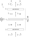
- Figure 10 illustrates an example of a display device 1000, e.g., a wearable display device, comprising one or more broadband adaptive lens assemblies, e.g., a pair of broadband adaptive lens assemblies 1004, 1008 in an optical path 1016 that are interposed by a waveguide assembly 1012.
- the waveguide assembly includes a waveguide configured to propagate light (e.g., visible light), e.g., under total internal reflection, and to outcouple the light in an optical axis extending from (e.g., in a direction normal to) a light output surface of the waveguide (e.g., a major surface of the waveguide).
- the light may be outcoupled by a diffraction grating in some embodiments.
- Each of the broadband adaptive lens assemblies 1004, 1008 may be configured to at least partially transmit outcoupled light therethrough.
- each of the adaptive lens assemblies may be configured to receive outcoupled light from the waveguide assembly 1012 and to converge or diverge the outcoupled light in the optical axis direction.
- Each of the broadband adaptive lens assemblies 1004, 1008 comprises a waveplate lens comprising liquid crystals arranged such that the waveplate lens has birefringence ( ⁇ n) that varies in a radial direction from a central region of the waveplate lens and that increases or decreases with increasing wavelength ( ⁇ ) within a range of the visible spectrum.
- the broadband adaptive lens assembly is configured to be selectively switched between a plurality of states having different optical powers.
- the broadband adaptive lens assembly is configured to alter a polarization state of the outcoupled light passing therethrough when activated (e.g., electrically activated).
- an adaptive lens assembly refers to a lens assembly having at least one optical property that may be adjusted, e.g., reversibly activated and deactivated, using an external stimulus.
- Example optical properties that may be reversibly activated and deactivated include, among other properties, optical power (focal length), phase, polarization, polarization-selectivity, transmissivity, reflectivity, birefringence and diffraction properties, among other properties.
- adaptive lens assemblies are capable of electrically varying the optical power and the polarization state of light passing therethrough.
- each of the pair of broadband adaptive lens assemblies 1004, 1008 is configured to be selectively switched between at least two states. In a first state, each is configured to pass the outcoupled light therethrough without altering a polarization state thereof, while in a second state, each is configured to alter the polarization state of the outcoupled light passing therethrough. For example, in the second state, each of the broadband adaptive lens assemblies 1004, 1008 reverses the handedness of circularly polarized light, while in the first state, each of the broadband adaptive lens assemblies 1004, 1008 preserves the handedness of circularly polarized light.
- the display device 1000 further comprises a waveguide assembly 1012 interposed between the pair of adaptive lens assemblies 1004, 1008.
- the waveguide assembly 1012 may be similar to the waveguide assembly 260 described above with respect to Figure 6 , which comprises one or more waveguides, similar to one or more waveguides 270, 280, 290, 300, 310 in Figure 6 .
- the waveguide may be configured to propagate light under total internal reflection in a lateral direction parallel to a major surface of the waveguide.
- the waveguide may further be configured to outcouple the light, e.g., in a direction normal to the major surface of the waveguide.
- a first adaptive lens assembly 1004 of the pair of adaptive lens assemblies is disposed on a first side of the waveguide assembly 1012, e.g., the side of the world 510 observed by a user
- a second adaptive lens assembly 1008 of the pair of lens assemblies is disposed on a second side of the waveguide assembly 1012, e.g., the side of the eye 210 of the user.
- the pair of adaptive lens assemblies as configured provides to a user virtual content from the waveguide assembly 1012 at a plurality of virtual depth planes, as well the view of the real world. In some embodiments, there is little or no distortion due to the presence of the adaptive lens assemblies.
- the virtual content and the view of the real world are provided to the user upon activation of the first and second adaptive lens assemblies 1004, 1008, as described infra with respect to Figures 11A and 11B .
- FIGS 11A and 11B illustrate examples of display devices 1100A/1100B, each comprising adaptive lens assemblies in operation to output image information to a user.
- the display devices 1100A and 1100B in an unpowered state are structurally identical.
- the display device 1100A is used herein to describe outputting virtual image to the user, while the display device 1100B is used herein to describe transmitting a real world image through the display device 1100B to the user.
- the display device 1100A/1100B includes a pair of the switchable lenses assemblies 1004, 1008 that are configured to be electrically activated by, e.g., application of a voltage or a current.
- each of the first and second switchable lenses assemblies 1004, 1008 has a low, e.g., about zero, optical power.
- the first adaptive lens assembly 1004 on the side of the world may provide a first net optical power (Pnet1) having a first sign, e.g., a positive optical power.
- the second adaptive lens assembly 1008 on the side of the user may provide a second net optical power (Pnet2) having a second sign, e.g., a negative optical power.
- Figure 11A illustrates an example of the display system of Figure 10 displaying virtual content to a user at a virtual depth plane, according to some embodiments.
- the waveguide assembly 1012 interposed between the pair of the adaptive lens assemblies 1004, 1008 comprises a waveguide configured to receive light containing virtual image information and to propagate the light under total internal reflection.
- the waveguide assembly 1012 is further configured to outcouple the light through, e.g., a diffraction grating, towards the eye 210.
- the outcoupled light passes through the second adaptive lens assembly 1008 prior to entering the eye 210.
- the second adaptive lens assembly 1008 has a second net optical power, Pnet2, which may have a negative value, such that the user sees the virtual image at a virtual depth plane 1104.
- the second adaptive lens assembly 1008 may be adjusted electrically to adjust the second net optical power (Pnet2) of the second adaptive lens assembly 1008, thereby adjusting the distance to the virtual depth plane 1104.
- Pnet2 the second net optical power of the second adaptive lens assembly 1008
- the magnitude of the distance to the virtual depth plane 1104 may be adjusted in discrete steps, while in some other embodiments, the magnitude of the distance to the virtual depth plane 1104 may be adjusted continuously.
- Figure 11B illustrates an example of the display system of Figure 10 providing a view of real world content to a user, according to some embodiments.
- the second adaptive lens assembly 1008 When the second adaptive lens assembly 1008 is activated to have the second net optical power (Pnet2) to display the virtual content at the virtual depth plane 1104, light from the real world passing through the second adaptive lens assembly 1008 may also be converged or diverged according to Pnet2 of the activated second adaptive lens assembly 1008. Thus, objects in the real world may appear out of focus.
- the first and second adaptive lens assemblies 1004, 1008 may be configured to have optical powers having opposite signs.
- light passing through the first and second adaptive lens assemblies 1004, 1008 converges or diverges according to a combined optical power having a magnitude that is about a difference between magnitudes of first and second net optical powers Pnet1, Pnet2, of the first and second adaptive lens assemblies 1004, 1008, respectively.
- the waveguide assembly 1012 may also have optical power and the adaptive lens assembly 1008 may be configured to account for the distortions caused by both the lens assembly 1004 and the waveguide assembly 1012.
- the optical power of the adaptive lens assembly 1008 may be opposite in sign to the sum of the optical powers of the lens assembly 1004 and the waveguide assembly 1012.
- the first adaptive lens assembly 1004 is configured to have the first net optical power Pnet1 that has a magnitude that is close to or the same as the magnitude of the second net optical power Pnet2 of the second adaptive lens assembly 1008, while having a sign that is opposite of Pnet2.
- the advantages of forming images at a plurality of depth planes with fewer waveguides includes the overall reduction in thickness and weight of the display device (e.g., display device 1000 in Figure 10 ).
- various embodiments described herein provide adaptive waveplate lens assemblies that are compact, lightweight and provide various optical functionalities, e.g., high bandwidth capability and variable optical power.
- various embodiments described herein provide adaptive lens assemblies with relatively low amount of leakage light.
- the broadband adaptive lens assembly includes a waveplate lens (1154A, 1154B in Figures 12A, 12B , respectively) comprising liquid crystals arranged such that the waveplate lens has birefringence ( ⁇ n) that varies in a radial direction from a central region of the first waveplate lens and that increases or decreases with increasing wavelength ( ⁇ ) within a range of the visible spectrum.
- the broadband adaptive waveplate lens assembly can generate images at multiple depth planes by being configured to be selectively switched between a plurality of states with different optical powers. The selective switching of the broadband lens assembly can in turn be performed by switching a waveplate lens or a waveplate included in the broadband adaptive wavelplate lens assembly according to embodiments, as discussed herein.
- the waveplate lens 1154A is configured such that it diverges or converges incident light 1162A, 1162B passing therethrough depending on the polarization of the light, e.g., circular polarization, according to various embodiments.
- the illustrated waveplate lens 1154A which may be a passive waveplate lens, is configured to converge a right-hand circular polarized (RHCP) light beam 1162B incident on the waveplate lens 1154A into a left-hand circular polarized (LHCP) light beam 1166A.
- the waveplate lens 1154A is configured to diverge a LHCP light beam 1162A incident on the waveplate lens 1154A into a right-hand circular polarized (RHCP) light beam 1166B.
- the polarization of the circularly polarized light passing therethrough is altered or flipped (illustrated). That is, the LHCP light beam 1166A is converted to a RHCP light beam 1170A and the RHCP light beam 1166B is converted to a LHCP light beam 1170B.
- the broadband adaptive lens assembly 1150B is configured to be switched between different optical power states by employing a switchable waveplate lens 1154B comprising liquid crystals.
- the adaptive lens assembly 1150B may be selectively switched between different states by electrically activating and deactivating the switchable waveplate lens 1154B.
- the broadband adaptive waveplate lens assembly can be used to generate images at multiple depth planes by selectively switching the broadband waveplate lens assembly between a plurality of lens states having different optical powers.
- the broadband adaptive waveplate lens assembly may be configured to be selectively switched between a plurality of lens states by electrically activating a broadband switchable waveplate included in the broadband adaptive waveplate lens assembly. In the following, embodiments of such broadband switchable waveplates are disclosed.
- broadband switchable waveplates comprise a layer of twisted nematic (TN) liquid crystals (LCs).
- Figure 13A illustrates a cross-sectional view of an example of a switchable waveplate comprising a layer of TN LCs.
- a TN LC switchable waveplate 1300A comprises a layer 1302 of TN LCs disposed between a pair of transparent substrates 1312. Each of the transparent substrates 1312 has formed on the inner surface a conducting transparent electrode 1316, 1320.
- the surfaces of the transparent electrodes 1316, 1320 and/or the substrates 1312 may be configured such that the TN LC molecules in contact with or immediately adjacent to the upper electrode 1316 tend to orient with their long axes extending in a first lateral direction, while the TN LC molecules in contact with or immediately adjacent to the lower electrode 1320 tend to orient with their long axes extending in a second lateral direction, which may cross, e.g., to form an angle of about 90 degrees relative to, the first lateral direction.
- the TN LC molecules between the TN LC molecules immediately adjacent to the lower electrode 1320 and the TN LC molecules immediately adjacent to the upper electrode 1316 undergo a twist.
- the illustrated TN LC switchable waveplate 1300A is configured as a broadband waveplate.
- the TN LC layer 1302 serves to shift the polarization direction of linearly polarized light passing therethrough from one linear polarization direction to another.
- the transmitted light 1304A is polarized in a second direction (same direction as the LC molecules closes to the upper electrodes 1316) opposite the first direction.
- the switchable broadband waveplate 1300B when the switchable broadband waveplate 1300B is deactivated (lower portion of FIG. 13B ), after the incident circularly polarized light beam 1324 passes through the first QWP 1324 as described above and subsequently passes through a deactivated TN LC switchable waveplate 1300A, the polarization of the first linearly polarized light beam 1328 is preserved. Thereafter, upon passing through the second QWP 1326, first linearly polarized light beam 1328 is transformed into an exiting circularly polarized light beam 1340 having the first handedness, e.g., into a LHCP light beam.
- the broadband waveplate 1300B serves as transparent medium which preserves the polarization of a circular polarized light beam.
- the first and/or second QWP 1324, 1326 are broadband quarter waveplates having similar bandwidths compared to the TN LC switchable waveplate 1300A.
- quarter waveplates 1324, 1326 can be formed using a polymerized TN LC layer.
- QWPs include a plurality of TN LC layers. When each of the TN LC layers are formed on its own substrate, the resulting broadband quarter waveplate and/or the optical absorption of the resulting stack may become unacceptably thick.
- embodiments of QWPs comprising a plurality of TN LC layers formed on a single substrate are described, for efficient integration with the TN LC switchable waveplate 1300A.
- Figure 13C illustrates a cross-sectional view of a broadband QWP 1300C, which can be the first and/or second QWP 1324, 1326 illustrated above with respect to Figure 13B , comprising a plurality (M number) of TN LC layers 1302-1, 1302-2,...1302-M, stacked on an alignment layer 1302-0 formed on a substrate 1312.
- the alignment layer 1302-0 which is further described elsewhere in the specification, is configured to induce the elongation direction of the LC molecules in the first TN LC layer 1302-1 that are immediately adjacent to the alignment layer 1302-0 to be aligned in a first direction.
- the LC molecules above the LC molecules aligned by the alignment layer 1302-0 successively undergo a first twist, such that the LC molecules in the first TN LC layer 1302-1 that are farthest from the alignment layer 1302-0, which are directly adjacent to the second TN LC layer 1302-2, are elongated in a second direction.
- the alignment of LC molecules in each of the subsequent TN LC layers 1302-2 to 1302-M are aligned in a similar manner as the first TN LC layer 1302-1 except, the LC molecules closest to the previous layer is aligned in the same direction as the topmost LC molecules of the previous layer.
- the pattern of nanostructures 1400A can be patterned on the substrate 1312 using, e.g., a lithographic or a nanoimprinting technique, described in detail elsewhere in the specification.
- the nanostructures can be formed of a sufficiently thin conducting material that is patterned as elongated metal wires.
- the conducting material can be gold, silver, copper, aluminum or ITO or any suitable conducting material having a thickness and electrical resistivity such that the resulting pattern of nanostructures can serve simultaneously as an alignment layer and as an electrode layer.
- the display device 1800A/1800B comprise a pair of adaptive lens assemblies 1004, 1008 in the optical path between the world 510 and the eye 210, where each of the pair of adaptive lens assemblies 1004, 1008 comprises a switchable waveplate (e.g., 1712A/1712B in Figures 17A / 17B ) configured to alter a polarization state of light passing therethrough when electrically deactivated.
- the pair of adaptive lens assemblies When electrically deactivated, the pair of adaptive lens assemblies have net optical powers (Pnetl, Pnet2) having opposite signs such that light passing through the pair of adaptive lens assemblies converges or diverges according to a combined optical power having a magnitude that is about a difference between magnitudes of optical powers the pair of adaptive lens assemblies.
- the virtual content may be observed by the user at a depth plane according to Pnet2, which may be negative, while the view of the world is relatively unaffected by Pnet2 that is at least partially compensated by Pnet1, which may be positive.
- local orientation directions of LC molecules, e.g., elongation directions, above the lowermost LC molecules can be generally the same as those of the lowermost LC molecules closest to the substrate. In some other embodiments, local orientation directions of LC molecules above the lowermost LC molecules can be generally different from those of the lowermost LC molecules closest to the substrate. For example, local orientation directions of LC molecules above the lowermost LC molecules can be successively twisted, as described infra (e.g., Figures 20A, 20B ).
- Figures 20A and 20B schematically illustrate a plan view and a cross-sectional view, respectively, of a broadband waveplate lens 2000 comprising crystal plurality of LC layers, according to embodiments.
- the illustrated broadband waveplate lens 2000 comprises a stack of two LC layers 2004, 2008 having LC molecules that have opposite twist sense, such that retardation of light by one of the LC layers 2004, 2008 is compensated by the other one of the LC layers 2004, 2008.
- Figures 20A and 20B depict the relative orientations of LC molecules that laterally vary schematically in a particular fashion.
- the LC layers 2004, 2008 by configuring the LC layers 2004, 2008 to have suitable thickness, e.g., between about 1 ⁇ m and 2 ⁇ m or between about 1.5 ⁇ m and 2 ⁇ m, for instance about 1.7 ⁇ m, and a suitable chiral twist between about 50 degrees and 90 degrees or between about 60 degrees and 80 degrees, for instance about 70 degrees, relative bandwidth ⁇ / ⁇ o greater than 40%, 50% or 60%, for instance about 56% can be achieved, within which wavelength range the diffraction efficiency is greater than 99%., according to embodiments.
- ⁇ n birefringence
- ⁇ wavelength
- d thickness
- optically anisotropic materials display ⁇ n which decreases with increasing ⁇ (referred to herein as a positive dispersion of ⁇ n).
- Figure 21 illustrates a cross-sectional view of a broadband waveplate lens 2100 comprising a negative dispersion (ND) liquid crystal (LC) layer 2104 formed on a substrate 1312 and an alignment layer 1312-0, according to embodiments.
- the ND LC layer 2104 can be arranged, e.g., by suitably arranging the alignment layer 1312-0, such that the waveplate lens 2100 has a birefringence ( ⁇ n) that varies in a radial direction from a central region.
- ⁇ n birefringence
- the bottommost LC molecules closest to the substrate 1312 can be arranged to generally have the same orientation direction at a given radius from the central region and to generally have orientation directions that vary as a function of radius, in a similar manner as described above with respect to Figures 16A, 16B and 19A using, e.g., an alignment layer 1312-0 that is suitably configured as discussed elsewhere in the specification.
- the negative dispersion (ND) liquid crystal (LC) layer 2104 can a have a within-layer birefringence ( ⁇ n) range of 0.01-0.05, 0.05-0.10, 0.15-0.20, 0.20-0.25, 0.25-0.30, 0.30-0.35, 0.35-0.40, or a value within a range defined by any of these values.
- the ND LC layer 2104 may be vertically homogenous.
- LC crystals formed above the bottommost LC molecules may not be twisted.
- the local director n may be substantially constant across the thickness of the ND LC layer 2104. In some other embodiments, within a given columnar region, the local director n may be substantially random across the thickness of the LC layer 2104.
- the ND LC layer 2104 may be formed of a material, e.g., reactive mesogens, having a material property such that ⁇ n increases with increasing wavelength ( ⁇ )within at least a portion of the visible spectrum within 400-800 nm, including one or more of a red spectrum which includes wavelengths in the range of about 620-780 nm, a green spectrum which includes wavelengths in the range of about 492-577 nm, and a blue spectrum in the range of about 435-493 nm, or within a range of wavelengths defined by any wavelength within the visible spectrum within about 400 nm to 800 nm, e.g., 400-700 nm, 430-650 nm or 450-630 nm.
- the NC LC layer 2104 has a dispersion of the extraordinary refractive index n e that is smaller than that of the ordinary refractive index n o .
- the ND LC layer 2104 comprises smectic liquid crystals (LC), e.g., a smectic LC-polymer composite material.
- LC smectic liquid crystals
- the broadband waveplate lens 2100 has a single ND LC layer 2104 having birefringence, unlike, e.g., the broadband waveplate lens 2000 described above with respect to Figures 20A and 20B having multiple layers.
- the LC layers can be configured to be passive or switchable, according to embodiments.
- the layer of LC molecules can be formed of polymerized LC (LCP), while when configured as a switchable lens, the layer of LC molecules can be formed of unpolymerized LC molecules or reactive mesogens.
- the waveplate lenses described above with respect to Figures 16A, 16B , 19A , 20A/20B and 21 further comprises transparent electrodes on both sides (e.g., Figure 14C ) or on the same side (e.g., Figures 15A/15B ) of the layer of LC molecules, in a similar manner as described above with respect to various embodiments describe above.
- Figures 22A-22C illustrate a switchable broadband waveplate lens 2200, which may be similar to any of the broadband waveplate lenses that described above with respect to any one of Figures 16A, 16B , 19A , 20A/20B and 21 , in operation.
- Figures 22A, 22B and 22C illustrate, respectively, a deactivated switchable broadband wavelplate lens 2200 having a LHCP light beam incident thereon, a deactivated switchable broadband wavelplate lens 2200 having a RHCP light beam incident thereon and an activated switchable broadband wavelplate lens 2200 having a LHCP light beam 1162A or RHCP light beam 1162B incident thereon.
- the switchable broadband waveplate lens 2200 comprises liquid crystals arranged as described above with respect to any one of Figures 16A, 16B , 19A , 20A/20B and 21 and is configured to be selectively switched between different lens states by electrically activating and deactivating.
- the switchable broadband waveplate lens 2200 is configured to diverge light according to optical power -P and to converge light according to optical power P depending on the polarization, e.g., circular polarization, of the incident light 1162A, 1162B, according to various embodiments.
- a switchable broadband waveplate lens can be configured such that when deactivated, it can exert optical powers P or -P, depending on the polarization of the incident light, while when activated, it can exert substantially no optical power.
- the inventors have recognized that, by combining two or more switchable broadband waveplate lenses, many more lens states can be obtained for displaying virtual images at many different depths of focus.
- broadband adaptive lens assemblies comprising a plurality of switchable broadband waveplate lenses are described where, by configuring the broadband waveplate lenses to have different optical powers, 2 n different optical power states can be obtained for an incident light having a given polarization.
- Figures 23A, 23B , 23C and 23D illustrate combinations of states in which the first switchable broadband waveplate lens 2304/second switchable broadband waveplate lens 2308 are deactivated/deactivated, deactivated/activated, activated/deactivated, and activated/activated, respectively.
- the first switchable broadband waveplate lens 2304 is configured in a similar manner compared to the broadband waveplate lens 2200 described above with respect to Figures 22A-22C . That is, when deactivated, the first switchable broadband waveplate lens 2304 is configured to diverge a LHCP light beam 1162A incident thereon into a RHCP beam 1166B according to an optical power -P1. In addition, while not illustrated, when deactivated, the first switchable broadband waveplate lens 2304 is configured to converge a RHCP light beam incident thereon into a LHCP beam according to an optical power +P1. On the other hand, when activated, the first switchable broadband waveplate lens 2304 is configured to substantially preserve the polarization of without substantially converging or diverging the circularly polarized light passing therethrough (i.e., optical power P1 ⁇ 0).
- the second switchable broadband waveplate lens 2308 is configured to operate in an opposite manner compared to the broadband waveplate lens 2200 described above with respect to Figures 22A-22C , with respect to the sign of the optical power exerted when deactivated. That is, when deactivated, the second switchable broadband waveplate lens 2308 is configured to converge a LHCP light beam 1162A incident thereon into a RHCP beam 1166B according to an optical power +P2. In addition, while not illustrated, when deactivated, the second switchable broadband waveplate lens 2308 is configured to diverge a RHCP light beam incident thereon into a LHCP beam according to an optical power -P2. On the other hand, when activated, the second switchable broadband waveplate lens 2308 is configured to substantially preserve the polarization of without substantially converging or diverging the circularly polarized light passing therethrough (i.e., optical power P2 ⁇ 0).
- the first switchable broadband waveplate lens 2304 is deactivated and diverges the LHCP light beam 1162A incident thereon into a RHCP light beam 1166B according to an optical power -P1.
- the second switchable broadband waveplate lens 2208 is deactivated and diverges the RHCP light beam 1166B incident thereon into a LHCP light beam 1170A according to an optical power -P2.
- the LHCP light beam 1162A incident on the broadband adaptive lens assembly 2300 is diverged into the LHCP light beam 1170A according to a net optical power of -(P1+P2).
- the first switchable broadband waveplate lens 2304 is activated and preserves the polarization of the LHCP light beam 1162A passing therethrough without substantially converging or diverging.
- the second switchable broadband waveplate lens 2308 is deactivated and converges the LHCP light beam 1162A incident thereon into a RHCP light beam 1170B according to optical power +P2.
- the LHCP light beam 1162B incident on the broadband adaptive lens assembly 2300 is converged into the RHCP light beam 1170B according to a net optical power of +P2.
- a broadband adaptive lens assembly 2300 can have four different optical power states of 0, -P1, +P2, and -(P1+P2), according to embodiments.
- the broadband adaptive lens assembly 2300 can have four different optical power states would be 0, +P1, -P2, and +(P1+P2).
- the second switchable broadband waveplate lens 2308 can be configured to operate in the same manner as the first switchable broadband waveplate lens 2304 in terms of the dependence of the sign of optical power on the polarization of the incident light.
- the incident light is a LHCP light beam
- the resulting four different optical power states would be 0, -P1, -P2, and -(P1-P2).
- the second switchable broadband waveplate lens 2308 is configured to operate in the same manner compared to the first broadband waveplate lens 2304 in terms of the dependence of the sign of optical power on the polarization of the incident light, when the incident light is a RHCP light beam, the resulting four different optical power states would be 0, P1, P2, and (P1-P2).
- the illustrated broadband adaptive lens assembly 2300 is configured to achieve variable optical powers by independently switching lenses themselves (e.g., first and second switchable broadband waveplate lenses 2304, 2308).
- first and second switchable broadband waveplate lenses 2204, 2208 are replaced by a combination of a passive waveplate lens and a switchable waveplate, similar to the combination of the passive waveplate lens 1154A and switchable waveplate 1158, as described above with respect to Figure 12a .
- FIG 24A illustrates of an integrated broadband adaptive lens assembly 2400 comprising a switchable layer of LC molecules similar to those described above with respect to any one of Figures 19A , 20A / 20B and 21 , according to embodiments.
- the integrated broadband adaptive lens assembly 2400 includes a switchable LC layer 2304, which can be similar to those described above with respect to any one of Figures 19A , 20A / 20B and 21 , except, the switchable LC layer 2304 is interposed between a pair of passive waveplate lens stacks 2308, 2312.
- the first passive waveplate lens stack 2308 includes a substrate 1312 on which a lower transparent electrode 1316 is formed, followed by an alignment layer 2302 and a lower polymerized LC (LCP) layer 2302-1.
- the second passive waveplate lens stack 2312 includes a substrate 1312 on which an upper transparent electrode 1320 is formed, followed by an alignment layer 2302 and an upper polymerized LC (LCP) layer 2302-2.
- Each of the first and second passive waveplate lens stacks 2308, 2312 serves as waveplate lenses as well as alignment layers for aligning LC molecules in the switchable LC layer 2304.
- the LC molecules of the lower LCP layer 2302-1 closest to the gap and the LC molecules of the upper LCP layer 2302-2 closest to the gap are arranged such that the outermost LC molecules of the switchable LC layer 2304 are self-aligned.
- the outermost LC molecules of the switchable LC layer 2204 may be sufficiently aligned by the upper and/or lower alignment layers 2302 such that one of both of the first and second LCP layers 2302-1, 2302-2 are omitted.
- a switchable LC layer e.g., the switchable LC layer 2304 inserted into the gap has a thickness of about 1 ⁇ m-50 ⁇ m, 1-10 ⁇ m, 10-20 ⁇ m, 20-30 ⁇ m, 30-40 ⁇ m, 40-50 ⁇ m or a value within any range defined by these values.
- passive LC layers e.g., the LCP layers 2302-1, 2302-2, can have a thickness of about 0.1 ⁇ m-50 ⁇ m, 0.1-1 ⁇ m, 1-10 ⁇ m, 10-20 ⁇ m, 20-30 ⁇ m, 30-40 ⁇ m, 40-50 ⁇ m or a value within any range defined by these values.
- each of the LCP layers 2302-1, 2302-2 can have LC molecules having a net twist angle of 30-90 degrees, 40-80 degrees, 50-70 degrees, or any angle within a range defined by any of these values, for instance about 60 degrees.
- the switchable LC layer 2304 can be a single layer, similar to the LC layer described above with respect to Figure 21 . However, embodiments are not so limited.
- the switchable LC layer 2204 can include a plurality of LC layers, in a similar manner as described above with respect to Figures 20A/20B .
- the integrated broadband adaptive lens assembly 2400 described herein with respect to Figure 24A share some characteristics that may be similar to the switchable waveplate 1300F described above with respect to Figure 13F .
- a switchable waveplate element (the switchable TN LC layer 1302 in Figure 13F and the switchable LC layer 2304 in Figure 24A ) is interposed between a pair of passive waveplate elements (the plurality of TN LC layers 1302-1, 1302-2 in Figure 13F , the polymerized LC (LCP) layers 2302-1, 2302-2).
- the switchable waveplate element is configured to change the polarization of light passing therethrough into an orthogonally polarized light.
- the passive waveplate elements are similarly aligned by respective alignment layers such that when the switchable waveplate element is electrically activated to pass light therethrough without diffracting, the passive waveplate elements have cancelling effects on each other.
- the switchable waveplate element is electrically deactivated to diffract light passing therethrough, the passive waveplate elements have complementary effects.
- the passive waveplate elements when the passive waveplate elements have the same optical power, and when the switchable waveplate element is activated, the net optical power of the assembly is about zero and the polarization of light is unaltered.
- the switchable waveplate element is deactivated, the net optical power of the assembly is a net sum of the powers of the switchable and passive waveplate elements having different signs.
- the passive waveplate elments are half waveplate lenses and the switchable waveplate element is also a half waveplate.
- FIGS 24B-24D illustrate the integrated broadband adaptive lens assembly 2400 in operation, which may be analogous to the adaptive lens assembly described above with respect to Figures 17A-17C except, the switchable half waveplate in the middle is configured as a lens exerting an optical power.
- Figure 24B illustrates the integrated broadband adaptive lens assembly 2400 described above with respect to Figure 24A in terms of optical functionality.
- Figure 24C illustrates the integrated broadband adaptive lens assembly 2400A ( Figure 24A ) in operation when the switchable waveplate lens 2304 of the adaptive lens assembly 2400 illustrated in Figure 24B is activated
- Figure 24D illustrates the switchable assembly 2400B in operation when the switchable waveplate lens 2304 of the integrated broadband adaptive lens assembly 2400 illustrated in Figure 24B is deactivated.
- the integrated broadband adaptive lens assembly 2400 is configured to couple and to transmit therethrough the light outcoupled from the waveguide assembly 1012 ( Figures 10 , 11A, 11B ).
- the integrated broadband adaptive lens assembly 2400 comprises a first waveplate lens (L1/HWP1) 2308 corresponding to the passive waveplate lens stack 2308 ( Figure 24A ), e.g., a first half-waveplate lens, a second waveplate lens (L2/HWP2) 2312 corresponding to the passive waveplate lens stack 2312 ( Figure 24A ), e.g., a second half-waveplate lens, and a switchable half waveplate (L3/HWP3) 2304 corresponding to the switchable LC layer 2304 ( Figure 24A ).
- L1/HWP1 first waveplate lens
- L2/HWP2 second waveplate lens
- L3/HWP3 switchable half waveplate
- the L3/HWP 2304B in a deactivated state ( Figure 24D )
- the L1/HWP1 2308 and the L2/HWP2 2312 serve as passive half waveplate lenses configured to exert optical powers P3, P1 and P2, respectively, and to flip the handedness of a circular polarized light passing therethrough from a first handedness (first HCP) to a second handedness (second HCP).
- the L3/HWP 2304A in an activated state ( Figure 24C ) is configured to preserve the handedness of the circular polarized light passing therethrough.
- the L3/HWP3 2304B ( Figure 24D ) serves as a half waveplate lens having an optical power P3.
- the L3/HWP3 2304A ( Figure 24C ) serves as transmitting medium for light without affecting the polarization or providing any substantial lensing effect.
- FIG 24C illustrates the integrated broadband adaptive lens assembly 2400B in operation when the L3/HWP 2304A is activated.
- the integrated broadband adaptive lens assembly 2400B may correspond to the first adaptive lens assembly 1004 ( Figure 10 , on the world side) or the second adaptive lens assembly 1008 ( Figure 10 , on the user side).
- integrated broadband adaptive lens assembly 2400A will be described as corresponding to the first adaptive lens assembly 1004 or the second adaptive lens assembly 1008, as part of the display device 1000 ( Figure 10 ) that is displaying the view of the real world to the user without displaying a virtual image.
- the display device 1000 ( Figure 10 ) may be used as ordinary eyeglasses or ordinary goggles.
- Each of the L1/HWP1 2308 and L2/HWP2 2312 may be configured to have a first lensing effect, e.g., diverging effect, on light having a first HCP, e.g., LHCP, passing therethrough. While not shown, each of the L1/HWP1 2308 and L2/HWP2 2312 may also be configured to have a second lensing effect opposite the first lensing effect, e.g., converging effect, on light having the opposite HCP, e.g., RHCP, passing therethrough.
- a first lensing effect e.g., diverging effect
- first HCP e.g., LHCP
- the L2/HWP2 2312 is configured similarly as the L1/HWP1 1704 ( Figure 17B ), i.e., to convert the polarization and to diverge light having LHCP while converging light having RHCP.
- a first lens effect e.g., converging effect
- Pnet1 (P1+P2+P3) having a first sign, e.g., positive sign.
- each of the first and second adaptive lens assemblies 1004, 1008 may provide a net optical power (positive or negative) in the range between about ⁇ 5.0 diopters and 0 diopters, ⁇ 4.0 diopters and 0 diopters, ⁇ 3.0 diopters and 0 diopters, ⁇ 2.0 diopters and 0 diopters, ⁇ 1.0 diopters and 0 diopters, including any range defined by these values, for instance ⁇ 1.5 diopters.
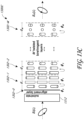
- FIGs 25A and 25B are graphs 2500A, 2500B illustrating transmission spectra corresponding to the integrated broadband adaptive lens assembly 2400 ( Figures 24A / 24B ) in which the L3/HWP3 2304 is deactivated ( Figure 24C ) and activated ( Figure 24D ), respectively.
- the simulations correspond to the integrated broadband adaptive lens assembly 2400 in which the L3/HWP3 2304 comprises a switchable LC layer 2304 formed of an unpolymerized LC layer (e.g., the switchable LC layer 2304 in Figure 23 ) of 10 ⁇ m in thickness and having ⁇ n of 0.2, while each of L1/HWP1 2308 and L2/HWP2 2312 comprises a polymerized LC layer formed of polymerized twisted LC molecules having a twist angle of 60 degrees (e.g., upper and lower polymerized LC (LCP) layers 2302-1, 2303-2 in Figure 24A ).
- LCP polymerized LC
- B, G, and R correspond to a wavelength in the blue spectrum, a wavelength in the green spectrum and a wavelength in the red spectrum, respectively.
- P net ((S 1 *P 1 + P 2 )*S 2 +P 3 )*S 3
- columns labeled State 1 to State 8 correspond to different lens states for each of the three lenses and rows BLUE, GREEN and RED represent calculated optical powers for at wavelengths of 450 nm, 525 nm and 632 nm, respectively, that are representative of blue, green and red colors of light.
- the optical powers of the three individual broadband waveplate lenses are calculated to be 0.5 D, 0.5 D, and 1.5 D at the green wavelength (525 nm).
- lens states 3, 5 and 1 can be selected.
- the net optical powers at blue and red wavelengths 450 nm and 632 nm
- can cause significant chromatic aberration e.g., as large as 0.51 D, for the target net optical power of 2.5 D for the red wavelength.
- chromatic aberration can be substantially reduced if, instead of using one state to achieve one target net optical power for the three colors as illustrated in TABLE 1, more than one state is used to achieve a given target net optical power for the different colors. This approach is illustrated in TABLE 2.
- the chromatic aberration can be substantially reduced.
- the optical powers of the three individual broadband waveplate lenses are 0.4 D, 0.7 D, and 1.6 D at the green wavelength (525 nm). Based on TABLE 2, it can be seen that to obtain target net optical power of 0.5 D, a single lens state 3 can be selected. However, to reduce chromatic aberration, for a target net optical power of 1.5 D, states 5 and 7 can be selected, and for a target net optical power of 2.5 D, states 1 and 5 can be selected.
- the chromatic aberration for the target net optical power of 2.5 D for the red wavelength can be reduced to 0.2.
- solid black lines 2612, 2622 and 2632 represent target net optical power
- dotted lines 2604, 2614 and 2624 represent calculated optical power when the method of using a single lens state to obtain a given optical power as described above with respect to TABLE 1 is used
- solid gray lines 2608, 2618 and 2628 represent calculated optical power when the method of using multiple lens states to obtain a given optical power as described above with respect to TABLE 2 is used.
- the actual powers are closer to the target power when multiple lens states to obtain a given optical power are used.
- the alignment layer 1302-0 can be a photo-alignment layer on which, when LC molecules are deposited, the LC molecules may become oriented along a preferential direction, for example, due to anchoring energy exerted on the liquid crystal molecule by the photo-alignment layer.
- photo-alignment layers include polyimide, linear-polarization photopolymerizable polymer (LPP), azo-containing polymers, courmarine-containing polymers and cinnamate-containing polymers, to name a few, as well as other compounds described above with respect to Figures 13C , 13F .
- the alignment layer 1302-0 may be formed by dissolving precursors, e.g., monomers, in a suitable solvent and coating the substrate 1312 with the solution using a suitable process, e.g., spin coating, slot coating, doctor blade coating, spray coating and jet (inkjet) coating, among other deposition processes. The solvent can thereafter be removed from the coated solution.
- the alignment layer 1302-0 may also be cured, e.g., UV cured, e.g., with a polarizer, in preparation for the subsequent alignment of the LC molecules thereon.
- the alignment layer 1302-0 is optically patterned or recorded.
- the optical patterning can be performed using a holographic two-beam exposure process ( Figure 28 ) or an optical replication process using a master lens and a one-beam exposure process ( Figures 29A, 29B ).
- a LC layer 2704 is formed thereon.
- the LC layer 2704 may be formed by depositing on the alignment layer 1302-0 a reactive mesogen mixture (including, e.g., liquid crystal monomers, solvents, photoinitiators, and surfactants) using a suitable process, including, e.g., spin coating, slot coating, doctor blade coating, spray coating and inkjet coating, among other deposition processes.
- a reactive mesogen mixture including, e.g., liquid crystal monomers, solvents, photoinitiators, and surfactants
- the LC layer 2704 may be cured, e.g., UV cured to photopolymerize the LC layer 2704, such that the LC molecules can become fixedly oriented, as described above.
- the LC layer 2704 when LC layer 2704 is integrated as part of a switchable waveplate lens or a switchable waveplate, the LC layer 2704 may be further processed without polymerizing the LC layer 2704, such that the LC molecules can reorient themselves in response to a switching signal as described above.
- the template is pressed into the blanket base polymer layer, which can include a thermoplastic polymer under certain temperature, e.g., above the glass transition temperature of the blanket base polymer layer, thereby transferring the pattern of the template into the softened blanket base polymer layer to form an imprinted alignment layer 3004.
- the template is separated from the imprinted alignment layer 3004, comprising an alignment pattern having predefined topological patterns configured to form an alignment pattern of LC molecules in the subsequently formed LC layer 2704 ( Figure 30B ).
- the imprinted alignment layer 3004 is hardened by crosslinking under UV light.
- the imprinted alignment layer 3004 can include features that are sub-wavelength in dimensions.
- the imprinted alignment layer 3004 can include features having dimensions (e.g., length, width and/or depth) of the order of a few nanometers, a few hundred nanometers and/or a few microns.
- the imprinted alignment layer 3004 can include features having a length greater than or equal to about 20 nm and less than or equal to about 100 nm.
- the imprinted alignment layer 3004 can include features having a width greater than or equal to about 20 nm and less than or equal to about 100 nm.
- the imprinted alignment layer 3004 can include features having a depth greater than or equal to about 10 nm and less than or equal to about 100 nm.
- the length and/or width of the features can be greater than the depth of the features.
- the depth can be approximately equal to the length and/or width of the features.
- the features of each domain of the imprinted alignment layer 3004 can be arranged to form complex geometric patterns within each domain in which the direction and/or the period between consecutive features changes along length scales of the order of a few nanometers, a few hundred nanometers and/or a few microns.
- an unpolymerized LC layer 2704 e.g., a layer of reactive mesogens, is deposited thereon, according to the deposition process described above with respect to Figures 27A-27C .
- the imprinted alignment layer 3004 serves as an alignment layer that causes the LC molecules of the LC layer 2704 to align according to the pattern of the imprinted alignment layer 3004.
- the elongation direction of LC molecules within a domain may generally align in a direction parallel to the local elongation direction of the nanostructures in the imprinted alignment layer 3004.
- the alignment of the LC molecules to the pattern of the imprinted alignment layer 3004 may be attributed to steric interactions with the liquid crystal molecules, and/or anchoring energy exerted on deposited LC molecules by the imprinted alignment layer 3004.
- Figure 30C illustrates a plan view of a nanoimprinted alignment layer 3004 that is fabricated according to the method described above with respect to Figures 30A-30B .
- the imprinted alignment layer 3004 can serve as an alignment layer to form a layer of LC molecules having various lateral arrangements as described herein including, e.g., the arrangements described above with respect to Figures 13A , 13C , 16A, 16B , 19A , among other arrangements.
- the imprinted alignment layer 3004 when LC layer resulting from the imprinted alignment layer 3004 forms part of a waveplate lens, the imprinted alignment layer 3004 according to various embodiments comprises a plurality of zones such as, for example, concentric zones 3008-1, 3008-2,...3008-n in the x-y plane, according to various embodiments.
- the imprinted nanostructures within each of the zones of the imprinted alignment layer 3004 are oriented along a particular orientation. The orientation of the molecules of the liquid crystal material in adjacent zones can be different.
- the elongated directions or the local directors of the LC molecules in the various zones zone 3008-1, 3008-2,...3008-n can be successively rotated in a radial direction according to a function that depends on a power of the radius r n from a central location, where n can vary from about 1 to 3 as described, for example, with respect to Figures 16A/16B and Figure 19 .
- the imprinted nanostructures and the resulting liquid crystal molecules can have elongation directions that are different in different zones 3008-1, 3008-2,...3008-n.
- the elongation direction of imprinted nanostructures in successive zones can be rotated in a clock-wise direction by an angle of about 18 degrees with respect each other.
- the relative rotation angle between successive zones can be less than 1 degree, between about 1 and 45 degrees, between about 1 and 18 degrees, or between about 18 and 45 degrees.
- broadband adaptive lens assemblies include integrated waveplates and waveplate lenses.
- methods of integrating the waveplates and waveplate lenses are described, according to embodiments.
- Figures 31A-31C illustrate an example method of fabricating a switchable broadband waveplate comprising liquid crystals or a switchable broadband waveplate lens comprising liquid crystals using a gap fill process.
- the method includes providing a lower stack including a first electrode layer on a first substrate and a first alignment layer formed on the first electrode layer, and includes providing an upper stack including a second electrode layer on a second substrate and a second alignment layer formed on the second electrode layer.
- the method includes providing a substrate 1312 in a similar manner as described above, e.g., with respect to Figure 27A , and thereafter forming on the substrate 1312 a first electrode layer 1320, e.g., a transparent electrode layer, in a similar manner as described above, e.g., with respect to Figure 27A .
- a first alignment layer 1302-0 is formed on the substrate 1312, thereby forming a lower stack 3100A.
- the alignment layer 1302-2 can be a photo-alignment layer similar to that described above with respect to, e.g., Figures 27A-27C , 28 and 29 , or an imprinted alignment layer similar to that described above with respect to, e.g., Figures 30A-30C .
- an upper stack 3100B is formed, comprising a second substrate 1312 on which a first electrode layer 1320, e.g., a transparent electrode layer, and a second alignment layer 1302-0 is formed in a similar manner as described above with respect to forming the lower stack 3100A, as described above with respect to Figure 31B .
- a first electrode layer 1320 e.g., a transparent electrode layer
- a second alignment layer 1302-0 is formed in a similar manner as described above with respect to forming the lower stack 3100A, as described above with respect to Figure 31B .
- the first and second alignment layers 1302-0 which may be photo-alignment layers or imprinted alignment layers, may be configured differently, as described above with respect to various embodiments, such that LC molecules immediately adjacent the first and second alignment layers 1302-0 align differently, e.g., align such that the elongation direction or the director direction of the LC molecules cross each other, e.g., at about 90 degrees.
- the upper and lower stacks 3100B, 3100A are subsequently stacked into a single stack, such that the first and second alignment layers 1302-0 face each other, where a gap 1302 is formed therebetween.
- the gap 1302 may be formed by spacers 1350 formed between the lower and upper stacks 3100A, 3100B.
- the spacers 1350 may be formed of a suitable material, e.g., silica beads having a diameter to produce the gap, whose distance defines the target thickness of the subsequently inserted LC material.
- the spacers 1350 in the form of silica beads can be dispersed using a dry process over the surface of one or both of the upper and lower stacks 3100B, 3100A.
- the spacers 1350 in the form of silica beads can be mixed with adhesives and applied at the edges of the surfaces of one or both of the upper and lower stacks 3100B, 3100A.
- upper and lower stacks 3100B, 3100A are pressed against each other, until a final gap distance corresponding to the resulting thickness of the LC layer, is obtained.
- the gap distance can be monitored using a Fabry-Perot interference fringes.
- a LC material is inserted into the gap 1302.
- the inserted LC material can be a reactive mesogen mixture including, e.g., liquid crystal monomers, solvents, photoinitiators, and surfactants, as described above.
- the LC material may be inserted in the gap 1302 by capillary force. In some implementations, the insertion is performed under vacuum.
- the integration process described above with respect to Figures 31A-31C can be applied to any suitable embodiment described herein.
- the method can be used to form a switchable broadband waveplate similar to that described above with respect to Figure 13F , including a pair of broadband QWP 1324, 1326 ( Figure 13F ) separated by the switchable TN LC layer 1302 ( Figure 13F ) inserted into the gap 1302 as described above.
- the lower stack 3100A includes a plurality of TN LC layers 1302-1, 1302-2 ( Figure 13F ) that are configured to serve as a QWP 1324 ( Figure 13B ), and the upper stack 3100B similarly includes a plurality of TN LC layers 1302-1, 1302-2 ( Figure 13F ) that are configured to serve as a QWP 1326 ( Figure 13B ).
- the integration process described above with respect to Figures 31A-31C can be applied to form an integrated broadband adaptive lens assembly similar to that described above with respect to Figure 24A , including a pair of polymerized LC (LCP) layers 2302-1, 2302-2 ( Figure 24A ) separated by the switchable LC layer 2304 ( Figure 24A ) inserted into the gap 1302 as described above to serve as the L3/HWP3 2304 ( Figures 23B-24D ).
- LCP polymerized LC
- the lower stack 3100A includes the lower polymerized LC (LCP) layer 2302-1 ( Figure 24A ) that serves as a Ll/HWP2 2308 ( Figures 24B-24D ), and the upper stack 3100B similarly includes the upper polymerized LC (LCP) layer 2302-2 ( Figure 24A ) that serves as a L2/HWP2 2312 ( Figures 24B-24D ).
- an example method of fabricating a switchable broadband waveplate comprising liquid crystals or a switchable broadband waveplate lens comprising liquid crystals employs a layer transfer process.
- a LC layer is formed on a donor, a sacrificial or a carrier substrate, which may be flexible, and thereafter be transferred to a permanent substrate, which may be rigid.
- the LC layer formation on such a carrier substrate may allow for higher manufacturing throughput and/or higher manufacturing yield.
- Figure 32A illustrates an intermediate structure 3200A comprising a carrier substrate 3204, which may be a suitable substrate having sufficient flexibility while having sufficient thermal stability for subsequent processes including polymerization of a LC layer, on which an alignment layer 1302-0 is formed.
- the alignment layer 1302-0 can be a photo-alignment layer formed and configured in a similar manner to those described above with respect to, e.g., Figures 27A-27C , 28 and 29 , or an imprinted alignment layer formed and configured in a manner similar to that described above with respect to, e.g., Figures 30A-30C .
- Figure 32B illustrates an intermediate structure 3200B comprising a release layer 3208 formed on the alignment layer 3208 and Figure 32C illustrates an intermediate structure 3200C comprising an LC layer 3212 formed on the release layer 3208, thereby temporarily bonding the LC layer 3212 on the alignment layer 3208.
- the LC layer 3212 can be formed and configured in a similar manner as describe above with respect to Figure 27C .
- the release layer 3208 comprises a thin surface layer formed by a surface treatment which weakens the adhesion strength between the LC layer 3212 and the alignment layer 1302-0 without substantially affecting the alignment properties of the alignment layer 3208.
- the broadband adaptive lens assembly further comprises a second waveplate lens comprising a second liquid crystal layer and a switchable waveplate interposed between the first waveplate lens and the second waveplate lens, wherein the broadband adaptive lens assembly is configured to be selectively switched between the at least two states by electrically activating and deactivating the switchable waveplate.
- the switchable waveplate comprises twisted nematic liquid crystals, and wherein electrically activating alters a degree twist of the twisted nematic liquid crystals across a thickness of the switchable waveplate.
- the switchable waveplate when the switchable waveplate is activated, serves as a half waveplate configured to invert the handedness of a circularly polarized light passing therethrough, while when the switchable waveplate is deactivated, the switchable waveplate is configured to conserve the handedness of the circularly polarized light passing therethrough.
- each of the first and second waveplate lenses is configured to invert the handedness of the circularly polarized light passing therethrough, and wherein when the switchable waveplate is activated, the first and second waveplate lenses exert optical powers having opposite signs.
- each of the first and second waveplate lenses is configured to invert the handedness of the circularly polarized light passing therethrough, and wherein when the switchable waveplate is deactivated, the first and second waveplate lenses exert optical powers having the same sign.
- the broadband adaptive lens assembly when the switchable waveplate is deactivated, has a net optical power having a magnitude that is proportional to a sum of magnitudes of optical powers of the first and second waveplate lenses, while when the switchable waveplate is in an activated state, the adaptive lens assembly has a net optical power having a magnitude that is proportional to a difference between magnitudes of optical powers the first and second waveplate lenses.
- the first and second waveplate lenses have optical powers having about the same magnitude, such that when the switchable waveplate is electrically activated, the net optical power is about zero.
- the first waveplate lens is electrically switchable
- the broadband adaptive lens assembly further comprises a second waveplate lens that is electrically switchable and comprises a second liquid crystal (LC) layer arranged such that the second waveplate lens has birefringence ( ⁇ n) that varies in a radially outward direction from a central region of the second waveplate lens and configured to diffract the outcoupled light at a diffraction efficiency greater than 90% within the wavelength range, wherein the broadband adaptive lens assembly is configured to be selectively switched between the at least two states by switching one or both of the first and second waveplate lenses.
- LC liquid crystal
- each of the first and second switchable waveplates when activated, serves as a half waveplate configured to invert the handedness of a circularly polarized light passing therethrough, while when deactivated, each of the first and second switchable waveplates is configured to conserve the handedness of the circularly polarized light passing therethrough.
- each of the first and second waveplate lenses is configured to have optical powers having opposite signs when passing therethrough circularly polarized light having opposite polarizations.
- the broadband adaptive lens assembly has a net optical power having a magnitude that is proportional to a sum of magnitudes of optical powers of the first and second waveplate lenses, such that by selectively activating one or both of the first and second waveplate lenses, for the given polarization of the outcoupled light, the broadband adaptive lens assembly is configured to be selectively switched between four states.
- one or more adaptive lens assemblies 1504-1 to 1504-3 may be disposed between individual ones of the waveguides 1012a, 1012b, and/or 1012c.
- conditional language used herein such as, among others, “can,” “could,” “might,” “may,” “e.g.,” and the like, unless specifically stated otherwise, or otherwise understood within the context as used, is generally intended to convey that certain embodiments include, while other embodiments do not include, certain features, elements and/or steps. Thus, such conditional language is not generally intended to imply that features, elements and/or steps are in any way required for one or more embodiments or that one or more embodiments necessarily include logic for deciding, with or without author input or prompting, whether these features, elements and/or steps are included or are to be performed in any particular embodiment.
Landscapes
- Physics & Mathematics (AREA)
- General Physics & Mathematics (AREA)
- Engineering & Computer Science (AREA)
- Optics & Photonics (AREA)
- Theoretical Computer Science (AREA)
- Nonlinear Science (AREA)
- Computer Hardware Design (AREA)
- Crystallography & Structural Chemistry (AREA)
- Chemical & Material Sciences (AREA)
- Mathematical Physics (AREA)
- Microelectronics & Electronic Packaging (AREA)
- Spectroscopy & Molecular Physics (AREA)
- General Engineering & Computer Science (AREA)
- Computer Graphics (AREA)
- Software Systems (AREA)
- Multimedia (AREA)
- Liquid Crystal (AREA)
- Diffracting Gratings Or Hologram Optical Elements (AREA)
- Mechanical Optical Scanning Systems (AREA)
- Eyeglasses (AREA)
- Polarising Elements (AREA)
- Optical Couplings Of Light Guides (AREA)
- Transforming Electric Information Into Light Information (AREA)
Claims (14)
- Anzeigevorrichtung (1000, 1100A, 1100B, 1700A, 1800A, 1800B), die umfasst:einen Wellenleiter (260, 1012), der dafür konfiguriert ist, Licht in einer seitlichen Richtung parallel zu einer Ausgangsfläche des Wellenleiters zu führen, wobei der Wellenleiter ferner dafür konfiguriert ist, das geführte Licht durch die Ausgangsfläche auszukoppeln; undeine adaptive Breitband-Linsenanordnung (1004, 1008, 1150A, 2300, 2400, 2400A, 2400B), die dafür ausgelegt ist, das ausgekoppelte Licht aus dem Wellenleiter einzukoppeln und durch sie hindurchzubeugen, wobei die adaptive Breitband-Linsenanordnung eine erste Wellenplattenlinse (1154A, 1704, 1804, 2204, 2308) umfasst, die eine Flüssigkristall- (LC) Schicht umfasst, die so ausgelegt ist, dass die erste Wellenplattenlinse eine Doppelbrechung (Δn) aufweist, die in einer radial nach außen gerichteten Richtung von einem zentralen Bereich der ersten Wellenplattenlinse variiert, und so konfiguriert ist, das ausgekoppelte Licht mit einer Beugungseffizienz von mehr als 90 % innerhalb eines Wellenlängenbereichs zu beugen, der mindestens 450 nm bis 630 nm umfasst,wobei eine radiale Anordnung der Δn der ersten Wellenplattenlinse, die sich aus Flüssigkristallmolekülen (1208) der LC-Schicht in einem gegebenen Radius von einer zentralen Achse der ersten Wellenplattenlinse mit im Wesentlichen demselben Drehwinkel ergibt, so ist, dass die erste Wellenplattenlinse Licht mit einer ersten Polarisation radial konvergiert, während sie Licht mit einer zweiten Polarisation, die der ersten Polarisation entgegengesetzt ist, radial divergiert,wobei die Δn der ersten Wellenplattenlinse (1154A, 1704, 1804, 2204, 2308) mit zunehmender Wellenlänge (γ) innerhalb des Wellenlängenbereichs zunimmt, undwobei die adaptive Breitband-Linsenanordnung dafür konfiguriert ist, selektiv zwischen einer Vielzahl von Zuständen mit unterschiedlichen optischen Leistungen umzuschalten.
- Anzeigevorrichtung nach Anspruch 1, wobei die adaptive Breitband-Linsenanordnung (1004, 1008, 1150A, 2300, 2400, 2400A, 2400B) eine Vielzahl von Flüssigkristallschichten umfasst, wobei jede der Flüssigkristallschichten Flüssigkristallmoleküle umfasst, die nacheinander in einer Schichtnormalrichtung verdreht sind.
- Anzeigevorrichtung (1000, 1100A, 1100B, 1700A, 1800A, 1800B) nach Anspruch 1, wobei, wenn das ausgekoppelte Licht eine Polarisation aufweist, die adaptive Breitband-Linsenanordnung (1004, 1008, 1150A, 2300, 2400, 2400A, 2400B) dafür konfiguriert ist, selektiv zwischen mindestens zwei Linsenzuständen umgeschaltet zu werden, die umfassen:einen ersten Linsenzustand, der dafür konfiguriert ist, das ausgekoppelte Licht mit einer Polarisation aus dem Wellenleiter gemäß einer ersten optischen Leistung zu konvergieren oder zu divergieren und die Polarisation des ausgekoppelten Lichts zu ändern; undeinen zweiten Linsenzustand, der dafür konfiguriert ist, das ausgekoppelte Licht mit der Polarisation aus dem Wellenleiter gemäß einer zweiten optischen Leistung zu konvergieren oder zu divergieren, ohne die Polarisation des ausgekoppelten Lichts zu ändern.
- Anzeigevorrichtung (1000, 1100A, 1100B, 1700A, 1800A, 1800B) nach Anspruch 3, wobei die adaptive Breitband-Linsenanordnung (1004, 1008, 1150A, 2300, 2400, 2400A, 2400B) ferner eine zweite Wellenplattenlinse (1708, 1808, 2312) umfasst, die eine zweite Flüssigkristallschicht und eine schaltbare Wellenplatte umfasst, die zwischen der ersten Wellenplattenlinse (1154A, 1704, 1804, 2204, 2308) und der zweiten Wellenplattenlinse angeordnet ist, wobei die adaptive Breitband-Linsenanordnung dafür ausgelegt ist, selektiv zwischen den mindestens zwei Zuständen durch elektrisches Aktivieren und Deaktivieren der schaltbaren Wellenplatte umgeschaltet zu werden.
- Anzeigevorrichtung (1000, 1100A, 1100B, 1700A, 1800A, 1800B) nach Anspruch 4, wobei die schaltbare Wellenplatte verdrillte nematische Flüssigkristalle umfasst, und wobei eine elektrische Aktivierung einen Verdrehungsgrad der verdrillten nematischen Flüssigkristalle über eine Dicke der schaltbaren Wellenplatte verändert.
- Anzeigevorrichtung (1000, 1100A, 1100B, 1700A, 1800A, 1800B) nach Anspruch 4, wobei, wenn die schaltbare Wellenplatte aktiviert ist, die schaltbare Wellenplatte als eine Halbwellenplatte dient, die dafür konfiguriert ist, die Händigkeit eines durch sie hindurchgehenden zirkular polarisierten Lichts umzukehren, während, wenn die schaltbare Wellenplatte deaktiviert ist, die schaltbare Wellenplatte dafür konfiguriert ist, die Händigkeit des durch sie hindurchgehenden zirkular polarisierten Lichts beizubehalten.
- Anzeigevorrichtung (1000, 1100A, 1100B, 1700A, 1800A, 1800B) nach einem der Ansprüche 1 bis 6, wobei jede der ersten und zweiten Wellenplattenlinsen dafür konfiguriert ist, die Händigkeit des durch sie hindurchgehenden zirkular polarisierten Lichts umzukehren, und wobei bei Aktivierung der schaltbaren Wellenplatte die erste und die zweite Wellenplattenlinse optische Kräfte mit entgegengesetzten Vorzeichen ausüben.
- Anzeigevorrichtung (1000, 1100A, 1100B, 1700A, 1800A, 1800B) nach einem der Ansprüche 1 bis 6, wobei jede der ersten und zweiten Wellenplattenlinsen dafür konfiguriert ist, die Händigkeit des durch sie hindurchgehenden zirkular polarisierten Lichts umzukehren, und wobei bei Deaktivierung der schaltbaren Wellenplatte die erste und die zweite Wellenplattenlinse optische Kräfte mit gleichem Vorzeichen ausüben.
- Anzeigevorrichtung (1000, 1100A, 1100B, 1700A, 1800A, 1800B) nach einem der Ansprüche 1-6, wobei, wenn die schaltbare Wellenplatte deaktiviert ist, die adaptive Breitband-Linsenanordnung (1004, 1008, 1150A, 2300, 2400, 2400A, 2400B) eine optische Nettoleistung mit einer Größe aufweist, die proportional zu einer Summe der Größen der optischen Leistungen der ersten und zweiten Wellenplattenlinsen ist, während, wenn die schaltbare Wellenplatte in einem aktivierten Zustand ist, die adaptive Linsenanordnung eine optische Nettoleistung mit einer Größe aufweist, die proportional zu einer Differenz zwischen den Größen der optischen Leistungen der ersten und der zweiten Wellenplattenlinse ist.
- Anzeigevorrichtung (1000, 1100A, 1100B, 1700A, 1800A, 1800B) nach Anspruch 9, wobei die erste und die zweite Wellenplattenlinse optische Leistungen aufweisen, die etwa die gleiche Größe haben, so dass, wenn die schaltbare Wellenplatte elektrisch aktiviert ist, die optische Nettoleistung etwa Null ist.
- Anzeigevorrichtung (1000, 1100A, 1100B, 1700A, 1800A, 1800B) nach einem der Ansprüche 1-3, wobei die erste Wellenplattenlinse (1154A, 1704, 1804, 2204, 2308) elektrisch schaltbar ist, wobei die adaptive Breitband-Linsenanordnung (1004, 1008, 1150A, 2300, 2400, 2400A, 2400B) ferner eine zweite Wellenplattenlinse (1708, 1808, 2312) umfasst, die elektrisch schaltbar ist und eine zweite Flüssigkristall- (LC) Schicht umfasst, die so ausgelegt ist, dass die zweite Wellenplattenlinse eine Doppelbrechung (Δn) aufweist, die in einer radial nach außen gerichteten Richtung von einem zentralen Bereich der zweiten Wellenplattenlinse variiert und so konfiguriert ist, dass sie das ausgekoppelte Licht mit einer Beugungseffizienz von mehr als 90 % innerhalb des Wellenlängenbereichs beugt, wobei die adaptive Breitband-Linsenanordnung dafür ausgelegt ist, selektiv zwischen den mindestens zwei Zuständen umgeschaltet zu werden, indem eine oder beide der ersten und zweiten Wellenplattenlinsen umgeschaltet werden.
- Anzeigevorrichtung (1000, 1100A, 1100B, 1700A, 1800A, 1800B) nach Anspruch 11, wobei im aktivierten Zustand jede der ersten und zweiten schaltbaren Wellenplatten als Halbwellenplatte dient, die dafür konfiguriert ist, die Händigkeit eines durch sie hindurchgehenden zirkular polarisierten Lichts umzukehren, während im deaktivierten Zustand jede der ersten und zweiten schaltbaren Wellenplatten dafür konfiguriert ist, die Händigkeit des durch sie hindurchgehenden zirkular polarisierten Lichts beizubehalten.
- Anzeigevorrichtung (1000, 1100A, 1100B, 1700A, 1800A, 1800B) nach Anspruch 12, wobei jede der ersten und zweiten Wellenplattenlinsen dafür konfiguriert ist, optische Kräfte mit entgegengesetzten Vorzeichen aufzuweisen, wenn zirkular polarisiertes Licht mit entgegengesetzten Polarisationen durch sie hindurchgeht.
- Anzeigevorrichtung (1000, 1100A, 1100B, 1700A, 1800A, 1800B) nach Anspruch 13, wobei die adaptive Breitband-Linsenanordnung (1004, 1008, 1150A, 2300, 2400, 2400A, 2400B) eine optische Nettoleistung mit einer Größe aufweist, die proportional zu einer Summe der Größen der optischen Leistungen der ersten und zweiten Wellenplattenlinsen ist, so dass durch selektives Aktivieren einer oder beider der ersten und zweiten Wellenplattenlinsen für die gegebene Polarisation des ausgekoppelten Lichts die adaptive Breitband-Linsenanordnung so ausgelegt ist, dass sie selektiv zwischen vier Zuständen umgeschaltet wird.
Priority Applications (1)
| Application Number | Priority Date | Filing Date | Title |
|---|---|---|---|
| EP25179673.6A EP4592996A3 (de) | 2017-10-26 | 2018-10-25 | Breitbandige adaptive linsenanordnung für anzeige der erweiterten realität |
Applications Claiming Priority (2)
| Application Number | Priority Date | Filing Date | Title |
|---|---|---|---|
| US201762577672P | 2017-10-26 | 2017-10-26 | |
| PCT/US2018/057604 WO2019084334A1 (en) | 2017-10-26 | 2018-10-25 | BROADBAND ADAPTIVE LENS ASSEMBLY FOR INCREASED REALITY DISPLAY |
Related Child Applications (2)
| Application Number | Title | Priority Date | Filing Date |
|---|---|---|---|
| EP25179673.6A Division EP4592996A3 (de) | 2017-10-26 | 2018-10-25 | Breitbandige adaptive linsenanordnung für anzeige der erweiterten realität |
| EP25179673.6A Division-Into EP4592996A3 (de) | 2017-10-26 | 2018-10-25 | Breitbandige adaptive linsenanordnung für anzeige der erweiterten realität |
Publications (3)
| Publication Number | Publication Date |
|---|---|
| EP3701516A1 EP3701516A1 (de) | 2020-09-02 |
| EP3701516A4 EP3701516A4 (de) | 2021-07-28 |
| EP3701516B1 true EP3701516B1 (de) | 2025-07-09 |
Family
ID=66247745
Family Applications (2)
| Application Number | Title | Priority Date | Filing Date |
|---|---|---|---|
| EP18871789.6A Active EP3701516B1 (de) | 2017-10-26 | 2018-10-25 | Breitbandige adaptive linsenanordnung für anzeige von erweiterter realität |
| EP25179673.6A Pending EP4592996A3 (de) | 2017-10-26 | 2018-10-25 | Breitbandige adaptive linsenanordnung für anzeige der erweiterten realität |
Family Applications After (1)
| Application Number | Title | Priority Date | Filing Date |
|---|---|---|---|
| EP25179673.6A Pending EP4592996A3 (de) | 2017-10-26 | 2018-10-25 | Breitbandige adaptive linsenanordnung für anzeige der erweiterten realität |
Country Status (9)
| Country | Link |
|---|---|
| US (4) | US11231612B2 (de) |
| EP (2) | EP3701516B1 (de) |
| JP (4) | JP7260538B2 (de) |
| KR (2) | KR102845935B1 (de) |
| CN (2) | CN111566723B (de) |
| AU (1) | AU2018355446A1 (de) |
| CA (1) | CA3079221A1 (de) |
| IL (2) | IL308526A (de) |
| WO (1) | WO2019084334A1 (de) |
Families Citing this family (46)
| Publication number | Priority date | Publication date | Assignee | Title |
|---|---|---|---|---|
| EP3701516B1 (de) | 2017-10-26 | 2025-07-09 | Magic Leap, Inc. | Breitbandige adaptive linsenanordnung für anzeige von erweiterter realität |
| US10466496B2 (en) * | 2017-12-06 | 2019-11-05 | Facebook Technologies, Llc | Compact multi-color beam combiner using a geometric phase lens |
| CN109975898A (zh) * | 2017-12-27 | 2019-07-05 | 华为技术有限公司 | 一种镜头模组和镜头模组的控制方法 |
| AU2019232746A1 (en) | 2018-03-07 | 2020-08-20 | Magic Leap, Inc. | Adaptive lens assemblies including polarization-selective lens stacks for augmented reality display |
| TWI664438B (zh) * | 2018-03-09 | 2019-07-01 | Industrial Technology Research Institute | 擴增實境裝置 |
| US11022791B2 (en) * | 2018-05-18 | 2021-06-01 | Facebook Technologies, Llc | Assemblies of anisotropic optical elements and methods of making |
| US11353767B2 (en) * | 2018-07-30 | 2022-06-07 | Facebook Technologies, Llc | Varifocal system using hybrid tunable liquid crystal lenses |
| US11822079B2 (en) | 2018-08-10 | 2023-11-21 | Apple Inc. | Waveguided display system with adjustable lenses |
| WO2020047486A1 (en) | 2018-08-31 | 2020-03-05 | Magic Leap, Inc. | Spatially-resolved dynamic dimming for augmented reality device |
| JP7136911B2 (ja) * | 2018-10-12 | 2022-09-13 | 富士フイルム株式会社 | 画像表示装置 |
| US10852619B1 (en) * | 2018-11-01 | 2020-12-01 | Facebook Technologies, Llc | Multifocal system using adaptive lenses |
| JP7153087B2 (ja) * | 2018-12-11 | 2022-10-13 | 富士フイルム株式会社 | 導光素子、画像表示装置およびセンシング装置 |
| WO2020146760A1 (en) | 2019-01-11 | 2020-07-16 | Magic Leap, Inc. | Time-multiplexed display of virtual content at various depths |
| US20220091420A1 (en) * | 2019-04-23 | 2022-03-24 | Directional Systems Tracking Limited | Augmented reality system |
| CN119620413A (zh) | 2019-07-04 | 2025-03-14 | 三星电子株式会社 | 用于显示增强现实的电子设备 |
| US11194080B2 (en) * | 2019-07-08 | 2021-12-07 | Samsung Electronics Co., Ltd. | Diffractive optical element and device |
| CN119045183A (zh) | 2019-07-12 | 2024-11-29 | 奇跃公司 | 用于具有动态视场的增强现实显示器的方法和系统 |
| US11099309B2 (en) * | 2019-08-23 | 2021-08-24 | Facebook Technologies, Llc | Outward coupling suppression in waveguide display |
| US11181741B1 (en) * | 2019-09-09 | 2021-11-23 | Facebook Technologies, Llc | Angularly selective dimming element, method of fabricating the same and optical device containing the same |
| US11467331B1 (en) * | 2019-10-29 | 2022-10-11 | Meta Platforms Technologies, Llc | Optical combiner with uniform illuminance throughput |
| CN114730111A (zh) * | 2019-11-22 | 2022-07-08 | 奇跃公司 | 用于对液晶层进行图案化的方法和系统 |
| US11733598B2 (en) * | 2019-12-04 | 2023-08-22 | Liqxtal Technology Inc. | Tunable light projector |
| JP7699835B2 (ja) * | 2019-12-30 | 2025-06-30 | イー-ビジョン スマート オプティックス, インク. | 高速電気活性レンズ切替システムおよび方法 |
| US11726328B2 (en) * | 2020-01-17 | 2023-08-15 | Meta Platforms Technologies, Llc | Accommodation adjustable and magnification corrective optical system |
| EP4104004A4 (de) * | 2020-02-11 | 2024-03-06 | Valve Corporation | Polarimetriekamera für oberflächencharakterisierungsmessungen mit hoher wiedergabetreue |
| US11108977B1 (en) * | 2020-02-20 | 2021-08-31 | Facebook Technologies, Llc | Dual wavelength eye imaging |
| US11526029B2 (en) * | 2020-08-19 | 2022-12-13 | E-Vision Smart Optics, Inc. | Electro-active sporting glasses |
| WO2022075820A1 (ko) * | 2020-10-08 | 2022-04-14 | 삼성전자주식회사 | 증강현실장치용 도파로의 회절광학소자 아키텍처 |
| CN114384698A (zh) * | 2020-10-19 | 2022-04-22 | 宏碁股份有限公司 | 拓展眼盒的智能眼镜 |
| US20220342121A1 (en) * | 2021-04-26 | 2022-10-27 | Meta Platforms Technologies, Llc | High index lens including uniaxial or biaxial organic solid material |
| US11782290B2 (en) * | 2021-05-21 | 2023-10-10 | Lightspace Group, Inc. | Apparatus and method for displaying three-dimensional image |
| US11693265B2 (en) | 2021-05-26 | 2023-07-04 | Meta Platforms Technologies, Llc | Polarization modulator |
| CN117813196A (zh) * | 2021-08-23 | 2024-04-02 | 根特大学 | 一种用于导出用于图案化平面光学部件的光对准层的自由曲面主透镜的表面轮廓的方法 |
| CN117813542A (zh) | 2021-09-13 | 2024-04-02 | 三星电子株式会社 | 用于具有宽视场的增强现实眼镜的基于衍射光学元件的波导架构 |
| EP4381340A4 (de) * | 2021-09-22 | 2024-11-20 | Samsung Electronics Co., Ltd. | Vorrichtung für erweiterte realität auf basis eines wellenleiters mit variabler krümmung, verfahren zum betrieb der vorrichtung für erweiterte realität, brille für erweiterte realität, optischer kompensator |
| US11921377B2 (en) * | 2021-12-02 | 2024-03-05 | Sharp Display Technology Corporation | Optical element, varifocal element, and head mounted display |
| CN114236819B (zh) * | 2021-12-29 | 2022-09-27 | 东南大学 | 一种基于偏振体全息光栅的波导显示二维扩瞳方法 |
| US11886094B2 (en) | 2022-02-21 | 2024-01-30 | Sharp Display Technology Corporation | Optical element, varifocal element and head mounted display |
| CN117554932B (zh) * | 2022-08-04 | 2025-07-04 | 荣耀终端股份有限公司 | Tof相机的遮挡检测方法及终端设备 |
| US20240272473A1 (en) * | 2023-02-15 | 2024-08-15 | Meta Platforms Technologies, Llc | High efficiency reflective liquid crystal polarization hologram for multi-wavelengths |
| US12117687B1 (en) | 2023-04-18 | 2024-10-15 | Meta Platforms Technologies, Llc | Liquid crystal polarization hologram with enhanced angular luminance uniformity and system including the same |
| WO2025023716A1 (ko) * | 2023-07-24 | 2025-01-30 | 삼성전자 주식회사 | 튜너블 렌즈를 포함하는 웨어러블 전자 장치 |
| CN116909026A (zh) * | 2023-08-02 | 2023-10-20 | 业成科技(成都)有限公司 | 头戴式显示装置 |
| US11971628B1 (en) * | 2023-09-05 | 2024-04-30 | Pixieray Oy | Compensation of chromatic aberration in liquid crystal elements |
| JP7692021B2 (ja) | 2023-09-27 | 2025-06-12 | シャープディスプレイテクノロジー株式会社 | 液晶素子及びヘッドマウントディスプレイ |
| KR102797696B1 (ko) * | 2023-12-07 | 2025-04-22 | 한국광기술원 | 편광의존성 능동형 초박형 홀로그래픽 광소자 |
Family Cites Families (279)
| Publication number | Priority date | Publication date | Assignee | Title |
|---|---|---|---|---|
| US3632865A (en) | 1969-12-23 | 1972-01-04 | Bell Telephone Labor Inc | Predictive video encoding using measured subject velocity |
| DE2737499C3 (de) | 1977-08-19 | 1981-10-22 | Max-Planck-Gesellschaft zur Förderung der Wissenschaften e.V., 3400 Göttingen | Faseroptisches Schaltungselement |
| JPS6010224A (ja) | 1983-06-29 | 1985-01-19 | Canon Inc | 焦点距離可変レンズ |
| GB8701288D0 (en) | 1987-01-21 | 1987-02-25 | Waldern J D | Perception of computer-generated imagery |
| US5271093A (en) | 1989-10-17 | 1993-12-14 | Mitsubishi Denki Kabushiki Kaisha | Video display apparatus for filling the interior shapes of contour |
| US5138555A (en) | 1990-06-28 | 1992-08-11 | Albrecht Robert E | Helmet mounted display adaptive predictive tracking |
| US8730129B2 (en) | 1990-12-07 | 2014-05-20 | Dennis J Solomon | Advanced immersive visual display system |
| US6222525B1 (en) | 1992-03-05 | 2001-04-24 | Brad A. Armstrong | Image controllers with sheet connected sensors |
| JPH0655203B2 (ja) | 1992-07-09 | 1994-07-27 | 株式会社エイ・ティ・アール視聴覚機構研究所 | 視線検出を用いた医療診断装置 |
| US5311897A (en) | 1992-09-18 | 1994-05-17 | Robert L. Cargill, Jr. | Rotary control valve with offset variable area orifice and bypass |
| JP3260867B2 (ja) | 1992-12-10 | 2002-02-25 | オリンパス光学工業株式会社 | 頭部装着型ディスプレイ |
| US5422653A (en) | 1993-01-07 | 1995-06-06 | Maguire, Jr.; Francis J. | Passive virtual reality |
| JP3306183B2 (ja) | 1993-09-14 | 2002-07-24 | リーダー電子株式会社 | 信号波形表示装置及び表示方法 |
| JP3630746B2 (ja) | 1994-12-05 | 2005-03-23 | キヤノン株式会社 | 画像観察装置 |
| US5742264A (en) | 1995-01-24 | 1998-04-21 | Matsushita Electric Industrial Co., Ltd. | Head-mounted display |
| US6882384B1 (en) * | 1995-05-23 | 2005-04-19 | Colorlink, Inc. | Color filters and sequencers using color selective light modulators |
| US5670988A (en) | 1995-09-05 | 1997-09-23 | Interlink Electronics, Inc. | Trigger operated electronic device |
| US5933125A (en) | 1995-11-27 | 1999-08-03 | Cae Electronics, Ltd. | Method and apparatus for reducing instability in the display of a virtual environment |
| JPH09284676A (ja) | 1996-04-15 | 1997-10-31 | Sony Corp | 身体の動きに同期した映像及び音声処理方法と映像表示装置 |
| US6151179A (en) | 1997-07-11 | 2000-11-21 | International Business Machines Corporation | Signal processing circuit with feedback extracted from a sampled analog error signal |
| WO1999022314A1 (en) | 1997-10-29 | 1999-05-06 | Sharp Kabushiki Kaisha | Display control device and reproduction display device for electronic books |
| JP2002110511A (ja) | 2000-09-27 | 2002-04-12 | Nikon Corp | 露光方法及び露光装置 |
| JP2001255862A (ja) | 2000-03-10 | 2001-09-21 | Seiko Epson Corp | オーバレイ画像処理装置およびオーバレイ画像表示装置 |
| US7663642B2 (en) | 2000-11-15 | 2010-02-16 | Sony Corporation | Systems and methods for rendering a polygon in an image to be displayed |
| DE10131720B4 (de) | 2001-06-30 | 2017-02-23 | Robert Bosch Gmbh | Head-Up Display System und Verfahren |
| US20030014212A1 (en) | 2001-07-12 | 2003-01-16 | Ralston Stuart E. | Augmented vision system using wireless communications |
| US6759979B2 (en) | 2002-01-22 | 2004-07-06 | E-Businesscontrols Corp. | GPS-enhanced system and method for automatically capturing and co-registering virtual models of a site |
| JP3762309B2 (ja) | 2002-02-18 | 2006-04-05 | キヤノン株式会社 | 位置方向測定装置および情報処理方法 |
| US7497574B2 (en) | 2002-02-20 | 2009-03-03 | Brother Kogyo Kabushiki Kaisha | Retinal image display device |
| BR0308099A (pt) * | 2002-03-13 | 2006-04-11 | E Vision Llc | lente eletro-óptica com componentes integrados |
| US6917370B2 (en) | 2002-05-13 | 2005-07-12 | Charles Benton | Interacting augmented reality and virtual reality |
| JP4170068B2 (ja) | 2002-11-12 | 2008-10-22 | シャープ株式会社 | データ信号線駆動方法、データ信号線駆動回路およびそれを用いた表示装置 |
| US7386799B1 (en) | 2002-11-21 | 2008-06-10 | Forterra Systems, Inc. | Cinematic techniques in avatar-centric communication during a multi-user online simulation |
| US7385606B2 (en) | 2002-12-18 | 2008-06-10 | Microsoft Corporation | International font measurement system and method |
| US7203384B2 (en) | 2003-02-24 | 2007-04-10 | Electronic Scripting Products, Inc. | Implement for optically inferring information from a planar jotting surface |
| US7515756B2 (en) | 2003-06-23 | 2009-04-07 | Shoestring Research, Llc. | Region segmentation and characterization systems and methods for augmented reality |
| US20050148388A1 (en) | 2003-07-17 | 2005-07-07 | Fabricio Vayra | Method and system for interaction with real-time events from a remote location, through use of a computer, game console or other module |
| ITTO20030662A1 (it) | 2003-08-29 | 2005-02-28 | Fiat Ricerche | Disposizione di visualizzazione virtuale per un quadro |
| US7110100B2 (en) | 2003-11-04 | 2006-09-19 | Electronic Scripting Products, Inc. | Apparatus and method for determining an inclination of an elongate object contacting a plane surface |
| KR101026800B1 (ko) | 2003-11-21 | 2011-04-04 | 삼성전자주식회사 | 액정 표시 장치, 표시 장치용 광원의 구동 장치 및 그방법 |
| US7038846B2 (en) | 2003-11-24 | 2006-05-02 | Electronic Scripting Products, Inc. | Solid catadioptric lens with a single viewpoint |
| US7268956B2 (en) | 2003-11-24 | 2007-09-11 | Electronic Scripting Products, Inc. | Solid catadioptric lens with two viewpoints |
| US7088440B2 (en) | 2003-12-22 | 2006-08-08 | Electronic Scripting Products, Inc. | Method and apparatus for determining absolute position of a tip of an elongate object on a plane surface with invariant features |
| US7826641B2 (en) | 2004-01-30 | 2010-11-02 | Electronic Scripting Products, Inc. | Apparatus and method for determining an absolute pose of a manipulated object in a real three-dimensional environment with invariant features |
| US8542219B2 (en) | 2004-01-30 | 2013-09-24 | Electronic Scripting Products, Inc. | Processing pose data derived from the pose of an elongate object |
| US7961909B2 (en) | 2006-03-08 | 2011-06-14 | Electronic Scripting Products, Inc. | Computer interface employing a manipulated object with absolute pose detection component and a display |
| US9229540B2 (en) | 2004-01-30 | 2016-01-05 | Electronic Scripting Products, Inc. | Deriving input from six degrees of freedom interfaces |
| US7729515B2 (en) | 2006-03-08 | 2010-06-01 | Electronic Scripting Products, Inc. | Optical navigation apparatus using fixed beacons and a centroid sensing device |
| US7023536B2 (en) | 2004-03-08 | 2006-04-04 | Electronic Scripting Products, Inc. | Apparatus and method for determining orientation parameters of an elongate object |
| US20050232530A1 (en) | 2004-04-01 | 2005-10-20 | Jason Kekas | Electronically controlled volume phase grating devices, systems and fabrication methods |
| US7161664B2 (en) | 2004-04-13 | 2007-01-09 | Electronic Scripting Products, Inc. | Apparatus and method for optical determination of intermediate distances |
| JP4373286B2 (ja) | 2004-05-06 | 2009-11-25 | オリンパス株式会社 | 頭部装着型表示装置 |
| US7403337B2 (en) | 2004-05-11 | 2008-07-22 | Universal Vision Biotechnology Co., Ltd. | Focus adjustable head mounted display system and method and device for realizing the system |
| US6947219B1 (en) | 2004-06-02 | 2005-09-20 | Universal Vision Biotechnology Co., Ltd. | Focus adjustable head mounted display system for displaying digital contents and device for realizing the system |
| US7113270B2 (en) | 2004-06-18 | 2006-09-26 | Electronics Scripting Products, Inc. | Determination of an orientation parameter of an elongate object with a scan beam apparatus |
| WO2005124431A1 (ja) | 2004-06-18 | 2005-12-29 | Pioneer Corporation | 情報表示装置、ナビゲーション装置 |
| US20060007056A1 (en) | 2004-07-09 | 2006-01-12 | Shu-Fong Ou | Head mounted display system having virtual keyboard and capable of adjusting focus of display screen and device installed the same |
| US8547401B2 (en) | 2004-08-19 | 2013-10-01 | Sony Computer Entertainment Inc. | Portable augmented reality device and method |
| JP4437731B2 (ja) * | 2004-10-08 | 2010-03-24 | フジノン株式会社 | 光ピックアップ光学系およびこれを用いた光ピックアップ装置 |
| US8585476B2 (en) | 2004-11-16 | 2013-11-19 | Jeffrey D Mullen | Location-based games and augmented reality systems |
| KR100656342B1 (ko) | 2004-12-16 | 2006-12-11 | 한국전자통신연구원 | 다중 입체 영상 혼합 제시용 시각 인터페이스 장치 |
| CN101846811A (zh) * | 2005-03-01 | 2010-09-29 | 荷兰聚合物研究所 | 介晶膜中的偏振光栅 |
| US20060214911A1 (en) | 2005-03-23 | 2006-09-28 | Eastman Kodak Company | Pointing device for large field of view displays |
| US20060226231A1 (en) | 2005-03-29 | 2006-10-12 | University Of Washington | Methods and systems for creating sequential color images |
| JP4738870B2 (ja) | 2005-04-08 | 2011-08-03 | キヤノン株式会社 | 情報処理方法、情報処理装置および遠隔複合現実感共有装置 |
| US7773098B2 (en) | 2005-05-11 | 2010-08-10 | Canon Kabushiki Kaisha | Virtual reality presentation apparatus and method |
| US8847861B2 (en) | 2005-05-20 | 2014-09-30 | Semiconductor Energy Laboratory Co., Ltd. | Active matrix display device, method for driving the same, and electronic device |
| US7737965B2 (en) | 2005-06-09 | 2010-06-15 | Honeywell International Inc. | Handheld synthetic vision device |
| US20060284791A1 (en) | 2005-06-21 | 2006-12-21 | National Applied Research Laboratories National Center For High-Performance Computing | Augmented reality system and method with mobile and interactive function for multiple users |
| IL173361A (en) | 2005-09-12 | 2012-03-29 | Elbit Systems Ltd | Display system near the eye |
| US20070081123A1 (en) | 2005-10-07 | 2007-04-12 | Lewis Scott W | Digital eyewear |
| US11428937B2 (en) | 2005-10-07 | 2022-08-30 | Percept Technologies | Enhanced optical and perceptual digital eyewear |
| US8696113B2 (en) | 2005-10-07 | 2014-04-15 | Percept Technologies Inc. | Enhanced optical and perceptual digital eyewear |
| US7480422B2 (en) | 2005-10-14 | 2009-01-20 | Disney Enterprises, Inc. | Systems and methods for information content delivery relating to an object |
| IL172797A (en) | 2005-12-25 | 2012-09-24 | Elbit Systems Ltd | Real-time image scanning and processing |
| JP2007240709A (ja) | 2006-03-07 | 2007-09-20 | Matsushita Electric Ind Co Ltd | 多焦点眼鏡 |
| SE0601216L (sv) | 2006-05-31 | 2007-12-01 | Abb Technology Ltd | Virtuell arbetsplats |
| US20080058629A1 (en) | 2006-08-21 | 2008-03-06 | University Of Washington | Optical fiber scope with both non-resonant illumination and resonant collection/imaging for multiple modes of operation |
| US7725547B2 (en) | 2006-09-06 | 2010-05-25 | International Business Machines Corporation | Informing a user of gestures made by others out of the user's line of sight |
| US7889178B2 (en) | 2006-09-08 | 2011-02-15 | Avago Technologies Ecbu Ip (Singapore) Pte. Ltd. | Programmable resolution for optical pointing device |
| US20080071559A1 (en) | 2006-09-19 | 2008-03-20 | Juha Arrasvuori | Augmented reality assisted shopping |
| JP4936522B2 (ja) | 2006-09-29 | 2012-05-23 | キヤノン株式会社 | 画像処理方法、画像処理装置 |
| JP5228307B2 (ja) | 2006-10-16 | 2013-07-03 | ソニー株式会社 | 表示装置、表示方法 |
| EP2089876A1 (de) | 2006-12-07 | 2009-08-19 | Adapx, Inc. | Systeme und verfahren zur kommentierung, aufzeichnung und übermittlung von daten |
| US7903166B2 (en) | 2007-02-21 | 2011-03-08 | Sharp Laboratories Of America, Inc. | Methods and systems for display viewer motion compensation based on user image data |
| US20080215974A1 (en) | 2007-03-01 | 2008-09-04 | Phil Harrison | Interactive user controlled avatar animations |
| JP5151207B2 (ja) | 2007-03-28 | 2013-02-27 | 株式会社ニコン | 表示装置 |
| US8339566B2 (en) * | 2007-04-16 | 2012-12-25 | North Carolina State University | Low-twist chiral liquid crystal polarization gratings and related fabrication methods |
| US8549415B2 (en) | 2007-05-04 | 2013-10-01 | Apple Inc. | Automatically adjusting media display in a personal display system |
| WO2009002567A1 (en) | 2007-06-27 | 2008-12-31 | The University Of Hawaii | Virtual reality overlay |
| US8902227B2 (en) | 2007-09-10 | 2014-12-02 | Sony Computer Entertainment America Llc | Selective interactive mapping of real-world objects to create interactive virtual-world objects |
| US20090089685A1 (en) | 2007-09-28 | 2009-04-02 | Mordecai Nicole Y | System and Method of Communicating Between A Virtual World and Real World |
| US8063905B2 (en) | 2007-10-11 | 2011-11-22 | International Business Machines Corporation | Animating speech of an avatar representing a participant in a mobile communication |
| US20090225001A1 (en) | 2007-11-06 | 2009-09-10 | University Of Central Florida Research Foundation, Inc. | Hybrid Display Systems and Methods |
| KR20090067822A (ko) | 2007-12-21 | 2009-06-25 | 삼성전자주식회사 | 현실 인자를 반영하는 혼합 세계 생성 시스템 및 구현 방법 |
| US20090177042A1 (en) | 2008-01-09 | 2009-07-09 | University Of Washington | Color image acquisition with scanning laser beam devices |
| US8615383B2 (en) | 2008-01-18 | 2013-12-24 | Lockheed Martin Corporation | Immersive collaborative environment using motion capture, head mounted display, and cave |
| US8624924B2 (en) | 2008-01-18 | 2014-01-07 | Lockheed Martin Corporation | Portable immersive environment using motion capture and head mounted display |
| US20090222424A1 (en) | 2008-02-26 | 2009-09-03 | Van Benedict | Method and apparatus for integrated life through virtual cities |
| US20100149073A1 (en) | 2008-11-02 | 2010-06-17 | David Chaum | Near to Eye Display System and Appliance |
| US8757812B2 (en) | 2008-05-19 | 2014-06-24 | University of Washington UW TechTransfer—Invention Licensing | Scanning laser projection display devices and methods for projecting one or more images onto a surface with a light-scanning optical fiber |
| US20090322671A1 (en) | 2008-06-04 | 2009-12-31 | Cybernet Systems Corporation | Touch screen augmented reality system and method |
| US8063968B2 (en) | 2008-07-23 | 2011-11-22 | Lockheed Martin Corporation | Device for detecting an image of a nonplanar surface |
| JP5651595B2 (ja) * | 2008-10-09 | 2015-01-14 | ノース・キャロライナ・ステイト・ユニヴァーシティ | 複数の偏光回折格子配置を有する偏光無依存型液晶ディスプレイ装置及び関連装置 |
| WO2010062481A1 (en) | 2008-11-02 | 2010-06-03 | David Chaum | Near to eye display system and appliance |
| US20100287500A1 (en) | 2008-11-18 | 2010-11-11 | Honeywell International Inc. | Method and system for displaying conformal symbology on a see-through display |
| EP2194418B1 (de) | 2008-12-02 | 2014-07-02 | Saab Ab | Head-Up-Anzeige für Nachtsichtbrillen |
| US20100137684A1 (en) | 2008-12-03 | 2010-06-03 | Hoya Corporation | Endoscope system with scanning function |
| US8132916B2 (en) | 2008-12-12 | 2012-03-13 | Carl Zeiss Meditec, Inc. | High precision contrast ratio display for visual stimulus |
| US8295546B2 (en) | 2009-01-30 | 2012-10-23 | Microsoft Corporation | Pose tracking pipeline |
| US8810758B2 (en) * | 2009-03-24 | 2014-08-19 | Jay Ahling | Dual-function alignment layer for liquid crystal devices to improve degradation resistance to radiation |
| US8487933B2 (en) | 2009-03-31 | 2013-07-16 | General Electric Company | System and method for multi-segment center point trajectory mapping |
| US9195898B2 (en) | 2009-04-14 | 2015-11-24 | Qualcomm Incorporated | Systems and methods for image recognition using mobile devices |
| WO2011014743A2 (en) * | 2009-07-31 | 2011-02-03 | North Carolina State University | Beam steering devices including stacked liquid crystal polarization gratings and related methods of operation |
| JP5553635B2 (ja) | 2009-10-23 | 2014-07-16 | キヤノン株式会社 | 補償光学装置、撮像装置および補償光学方法、撮像方法 |
| WO2011061914A1 (ja) | 2009-11-19 | 2011-05-26 | パナソニック株式会社 | 走査型画像表示装置 |
| WO2011070139A1 (en) * | 2009-12-10 | 2011-06-16 | Essilor International (Compagnie Generale D'optique) | An ophthalmic lens arrangement and an apparatus for demonstrating a plurality of optical functions and a method for demonstrating a plurality of optical functions |
| KR101652311B1 (ko) | 2010-01-26 | 2016-08-30 | 광주과학기술원 | 비전 영상 정보 저장 시스템과 그 방법, 및 상기 방법을 구현하는 프로그램이 기록된 기록매체 |
| JP5499762B2 (ja) | 2010-02-24 | 2014-05-21 | ソニー株式会社 | 画像処理装置、画像処理方法、プログラム及び画像処理システム |
| JPWO2011105581A1 (ja) * | 2010-02-26 | 2013-06-20 | 旭硝子株式会社 | 光学ローパスフィルタおよびデジタルカメラ |
| KR20130000401A (ko) | 2010-02-28 | 2013-01-02 | 오스터하우트 그룹 인코포레이티드 | 대화형 머리장착식 아이피스 상의 지역 광고 컨텐츠 |
| US20120249797A1 (en) | 2010-02-28 | 2012-10-04 | Osterhout Group, Inc. | Head-worn adaptive display |
| US8467133B2 (en) | 2010-02-28 | 2013-06-18 | Osterhout Group, Inc. | See-through display with an optical assembly including a wedge-shaped illumination system |
| US20120120103A1 (en) | 2010-02-28 | 2012-05-17 | Osterhout Group, Inc. | Alignment control in an augmented reality headpiece |
| US8482859B2 (en) | 2010-02-28 | 2013-07-09 | Osterhout Group, Inc. | See-through near-eye display glasses wherein image light is transmitted to and reflected from an optically flat film |
| JP2011203823A (ja) | 2010-03-24 | 2011-10-13 | Sony Corp | 画像処理装置、画像処理方法及びプログラム |
| US8893022B2 (en) | 2010-04-01 | 2014-11-18 | Microsoft Corporation | Interactive and shared viewing experience |
| JP5587403B2 (ja) | 2010-04-28 | 2014-09-10 | パナソニック株式会社 | 走査型画像表示装置 |
| US8762041B2 (en) | 2010-06-21 | 2014-06-24 | Blackberry Limited | Method, device and system for presenting navigational information |
| US20120200600A1 (en) | 2010-06-23 | 2012-08-09 | Kent Demaine | Head and arm detection for virtual immersion systems and methods |
| US20130120706A1 (en) | 2010-08-09 | 2013-05-16 | Panasonic Corporation | Optical device and charging system including the same |
| US8184215B2 (en) * | 2010-08-17 | 2012-05-22 | Lc-Tec Displays Ab | High-speed liquid crystal polarization modulator |
| US20120127136A1 (en) | 2010-08-18 | 2012-05-24 | Kent Displays Incorporated | Display device including piezoelectric and liquid crystal layers |
| US9111498B2 (en) | 2010-08-25 | 2015-08-18 | Eastman Kodak Company | Head-mounted display with environmental state detection |
| WO2012048252A1 (en) | 2010-10-07 | 2012-04-12 | Aria Glassworks, Inc. | System and method for transitioning between interface modes in virtual and augmented reality applications |
| US8578299B2 (en) | 2010-10-08 | 2013-11-05 | Industrial Technology Research Institute | Method and computing device in a system for motion detection |
| US8884984B2 (en) | 2010-10-15 | 2014-11-11 | Microsoft Corporation | Fusing virtual content into real content |
| US9122053B2 (en) | 2010-10-15 | 2015-09-01 | Microsoft Technology Licensing, Llc | Realistic occlusion for a head mounted augmented reality display |
| US9292973B2 (en) | 2010-11-08 | 2016-03-22 | Microsoft Technology Licensing, Llc | Automatic variable virtual focus for augmented reality displays |
| US8576276B2 (en) | 2010-11-18 | 2013-11-05 | Microsoft Corporation | Head-mounted display device which provides surround video |
| US9304319B2 (en) | 2010-11-18 | 2016-04-05 | Microsoft Technology Licensing, Llc | Automatic focus improvement for augmented reality displays |
| US8831278B2 (en) | 2010-11-30 | 2014-09-09 | Eastman Kodak Company | Method of identifying motion sickness |
| US8988463B2 (en) | 2010-12-08 | 2015-03-24 | Microsoft Technology Licensing, Llc | Sympathetic optic adaptation for see-through display |
| US9213405B2 (en) | 2010-12-16 | 2015-12-15 | Microsoft Technology Licensing, Llc | Comprehension and intent-based content for augmented reality displays |
| US9690099B2 (en) | 2010-12-17 | 2017-06-27 | Microsoft Technology Licensing, Llc | Optimized focal area for augmented reality displays |
| US10156722B2 (en) | 2010-12-24 | 2018-12-18 | Magic Leap, Inc. | Methods and systems for displaying stereoscopy with a freeform optical system with addressable focus for virtual and augmented reality |
| US9348143B2 (en) | 2010-12-24 | 2016-05-24 | Magic Leap, Inc. | Ergonomic head mounted display device and optical system |
| US20120182313A1 (en) | 2011-01-13 | 2012-07-19 | Pantech Co., Ltd. | Apparatus and method for providing augmented reality in window form |
| US9113050B2 (en) | 2011-01-13 | 2015-08-18 | The Boeing Company | Augmented collaboration system |
| US20120188148A1 (en) | 2011-01-24 | 2012-07-26 | Microvision, Inc. | Head Mounted Meta-Display System |
| JP2012155655A (ja) | 2011-01-28 | 2012-08-16 | Sony Corp | 情報処理装置、報知方法及びプログラム |
| JP5844288B2 (ja) | 2011-02-01 | 2016-01-13 | パナソニック インテレクチュアル プロパティ コーポレーション オブアメリカPanasonic Intellectual Property Corporation of America | 機能拡張装置、機能拡張方法、機能拡張プログラム、及び集積回路 |
| US9217867B2 (en) | 2011-03-24 | 2015-12-22 | Seiko Epson Corporation | Head-mounted display device and control method for the head-mounted display device |
| US8401343B2 (en) | 2011-03-27 | 2013-03-19 | Edwin Braun | System and method for defining an augmented reality character in computer generated virtual reality using coded stickers |
| US9071709B2 (en) | 2011-03-31 | 2015-06-30 | Nokia Technologies Oy | Method and apparatus for providing collaboration between remote and on-site users of indirect augmented reality |
| BR112013034009A2 (pt) | 2011-05-06 | 2017-02-07 | Magic Leap Inc | mundo de presença digital remota simultânea massiva |
| US8508830B1 (en) | 2011-05-13 | 2013-08-13 | Google Inc. | Quantum dot near-to-eye display |
| US20120327116A1 (en) | 2011-06-23 | 2012-12-27 | Microsoft Corporation | Total field of view classification for head-mounted display |
| US8934015B1 (en) | 2011-07-20 | 2015-01-13 | Google Inc. | Experience sharing |
| US20130021226A1 (en) | 2011-07-21 | 2013-01-24 | Jonathan Arnold Bell | Wearable display devices |
| AU2011204946C1 (en) | 2011-07-22 | 2012-07-26 | Microsoft Technology Licensing, Llc | Automatic text scrolling on a head-mounted display |
| AU2011205223C1 (en) | 2011-08-09 | 2013-03-28 | Microsoft Technology Licensing, Llc | Physical interaction with virtual objects for DRM |
| US10019962B2 (en) | 2011-08-17 | 2018-07-10 | Microsoft Technology Licensing, Llc | Context adaptive user interface for augmented reality display |
| US9342610B2 (en) | 2011-08-25 | 2016-05-17 | Microsoft Technology Licensing, Llc | Portals: registered objects as virtualized, personalized displays |
| WO2013032955A1 (en) | 2011-08-26 | 2013-03-07 | Reincloud Corporation | Equipment, systems and methods for navigating through multiple reality models |
| US9191661B2 (en) | 2011-08-29 | 2015-11-17 | Microsoft Technology Licensing, Llc | Virtual image display device |
| US9213163B2 (en) | 2011-08-30 | 2015-12-15 | Microsoft Technology Licensing, Llc | Aligning inter-pupillary distance in a near-eye display system |
| US9323325B2 (en) | 2011-08-30 | 2016-04-26 | Microsoft Technology Licensing, Llc | Enhancing an object of interest in a see-through, mixed reality display device |
| US8223024B1 (en) | 2011-09-21 | 2012-07-17 | Google Inc. | Locking mechanism based on unnatural movement of head-mounted display |
| EP2760363A4 (de) | 2011-09-29 | 2015-06-24 | Magic Leap Inc | Taktiler handschuh zur mensch-computer-interaktion |
| US9268406B2 (en) | 2011-09-30 | 2016-02-23 | Microsoft Technology Licensing, Llc | Virtual spectator experience with a personal audio/visual apparatus |
| US9286711B2 (en) | 2011-09-30 | 2016-03-15 | Microsoft Technology Licensing, Llc | Representing a location at a previous time period using an augmented reality display |
| US9255813B2 (en) | 2011-10-14 | 2016-02-09 | Microsoft Technology Licensing, Llc | User controlled real object disappearance in a mixed reality display |
| WO2013085639A1 (en) | 2011-10-28 | 2013-06-13 | Magic Leap, Inc. | System and method for augmented and virtual reality |
| US8752963B2 (en) | 2011-11-04 | 2014-06-17 | Microsoft Corporation | See-through display brightness control |
| US8879155B1 (en) | 2011-11-09 | 2014-11-04 | Google Inc. | Measurement method and system |
| US9311883B2 (en) | 2011-11-11 | 2016-04-12 | Microsoft Technology Licensing, Llc | Recalibration of a flexible mixed reality device |
| US20130141419A1 (en) | 2011-12-01 | 2013-06-06 | Brian Mount | Augmented reality with realistic occlusion |
| US8872853B2 (en) | 2011-12-01 | 2014-10-28 | Microsoft Corporation | Virtual light in augmented reality |
| US8963805B2 (en) | 2012-01-27 | 2015-02-24 | Microsoft Corporation | Executable virtual objects associated with real objects |
| WO2013119221A1 (en) | 2012-02-08 | 2013-08-15 | Intel Corporation | Augmented reality creation using a real scene |
| US9147111B2 (en) | 2012-02-10 | 2015-09-29 | Microsoft Technology Licensing, Llc | Display with blocking image generation |
| US20130215230A1 (en) | 2012-02-22 | 2013-08-22 | Matt Miesnieks | Augmented Reality System Using a Portable Device |
| JP5958689B2 (ja) | 2012-03-22 | 2016-08-02 | セイコーエプソン株式会社 | 頭部装着型表示装置 |
| US8933912B2 (en) | 2012-04-02 | 2015-01-13 | Microsoft Corporation | Touch sensitive user interface with three dimensional input sensor |
| KR102095330B1 (ko) | 2012-04-05 | 2020-03-31 | 매직 립, 인코포레이티드 | 능동 포비에이션 능력을 갖는 와이드-fov(field of view) 이미지 디바이스들 |
| US9183676B2 (en) | 2012-04-27 | 2015-11-10 | Microsoft Technology Licensing, Llc | Displaying a collision between real and virtual objects |
| US9122321B2 (en) | 2012-05-04 | 2015-09-01 | Microsoft Technology Licensing, Llc | Collaboration environment using see through displays |
| US9671566B2 (en) | 2012-06-11 | 2017-06-06 | Magic Leap, Inc. | Planar waveguide apparatus with diffraction element(s) and system employing same |
| US9201625B2 (en) | 2012-06-22 | 2015-12-01 | Nokia Technologies Oy | Method and apparatus for augmenting an index generated by a near eye display |
| US9645394B2 (en) | 2012-06-25 | 2017-05-09 | Microsoft Technology Licensing, Llc | Configured virtual environments |
| US9696547B2 (en) | 2012-06-25 | 2017-07-04 | Microsoft Technology Licensing, Llc | Mixed reality system learned input and functions |
| US9035970B2 (en) | 2012-06-29 | 2015-05-19 | Microsoft Technology Licensing, Llc | Constraint based information inference |
| US9841537B2 (en) | 2012-07-02 | 2017-12-12 | Nvidia Corporation | Near-eye microlens array displays |
| US9557565B2 (en) | 2012-07-02 | 2017-01-31 | Nvidia Corporation | Near-eye optical deconvolution displays |
| JP6015250B2 (ja) | 2012-08-31 | 2016-10-26 | 富士通株式会社 | 画像処理装置、画像処理方法及び画像処理プログラム |
| KR20150054967A (ko) | 2012-09-11 | 2015-05-20 | 매직 립, 인코포레이티드 | 인체공학적 헤드 마운티드 디스플레이 디바이스 및 광학 시스템 |
| US20140071163A1 (en) | 2012-09-11 | 2014-03-13 | Peter Tobias Kinnebrew | Augmented reality information detail |
| US10269179B2 (en) | 2012-10-05 | 2019-04-23 | Elwha Llc | Displaying second augmentations that are based on registered first augmentations |
| US10073201B2 (en) | 2012-10-26 | 2018-09-11 | Qualcomm Incorporated | See through near-eye display |
| US9619911B2 (en) | 2012-11-13 | 2017-04-11 | Qualcomm Incorporated | Modifying virtual object display properties |
| US9030495B2 (en) | 2012-11-21 | 2015-05-12 | Microsoft Technology Licensing, Llc | Augmented reality help |
| US9582123B2 (en) | 2012-11-26 | 2017-02-28 | Qualcomm Incorporated | Dual-mode capacitance sensing in a touch panel sensor |
| US20140178029A1 (en) | 2012-12-26 | 2014-06-26 | Ali Fazal Raheman | Novel Augmented Reality Kiosks |
| US9071390B2 (en) | 2013-01-10 | 2015-06-30 | Qualcomm Incorporated | Adjusting physical layer transmission properties |
| KR102274413B1 (ko) | 2013-01-15 | 2021-07-07 | 매직 립, 인코포레이티드 | 초고해상도 스캐닝 섬유 디스플레이 |
| US9342929B2 (en) | 2013-01-22 | 2016-05-17 | Microsoft Technology Licensing, Llc | Mixed reality experience sharing |
| JP2014149712A (ja) | 2013-02-01 | 2014-08-21 | Sony Corp | 情報処理装置、端末装置、情報処理方法及びプログラム |
| KR102050897B1 (ko) | 2013-02-07 | 2019-12-02 | 삼성전자주식회사 | 음성 대화 기능을 구비한 휴대 단말기 및 이의 음성 대화 방법 |
| IL298018B2 (en) | 2013-03-11 | 2024-04-01 | Magic Leap Inc | System and method for augmentation and virtual reality |
| EP2936220B1 (de) | 2013-03-13 | 2022-11-16 | ImagineOptix Corporation | Polarisationsumwandlungssystem mit geometrischen phasenhologrammen |
| US8970709B2 (en) | 2013-03-13 | 2015-03-03 | Electronic Scripting Products, Inc. | Reduced homography for recovery of pose parameters of an optical apparatus producing image data with structural uncertainty |
| US9852512B2 (en) | 2013-03-13 | 2017-12-26 | Electronic Scripting Products, Inc. | Reduced homography based on structural redundancy of conditioned motion |
| US9164281B2 (en) | 2013-03-15 | 2015-10-20 | Honda Motor Co., Ltd. | Volumetric heads-up display with dynamic focal plane |
| CN107656617B (zh) | 2013-03-15 | 2020-08-25 | 奇跃公司 | 显示系统和方法 |
| CN105408815A (zh) | 2013-03-15 | 2016-03-16 | 兰斯维克托公司 | 用于多液晶单元透镜的改进聚焦的方法和装置 |
| US9685003B2 (en) | 2013-06-03 | 2017-06-20 | Microsoft Technology Licensing, Llc | Mixed reality data collaboration |
| US9874749B2 (en) | 2013-11-27 | 2018-01-23 | Magic Leap, Inc. | Virtual and augmented reality systems and methods |
| US10262462B2 (en) | 2014-04-18 | 2019-04-16 | Magic Leap, Inc. | Systems and methods for augmented and virtual reality |
| US10139623B2 (en) | 2013-06-18 | 2018-11-27 | Microsoft Technology Licensing, Llc | Virtual object orientation and visualization |
| US10194860B2 (en) | 2013-09-11 | 2019-02-05 | Industrial Technology Research Institute | Virtual image display system |
| US9911231B2 (en) | 2013-10-08 | 2018-03-06 | Samsung Electronics Co., Ltd. | Method and computing device for providing augmented reality |
| KR20230098359A (ko) | 2013-10-16 | 2023-07-03 | 매직 립, 인코포레이티드 | 조절가능한 동공간 거리를 가지는 가상 또는 증강 현실 헤드셋들 |
| JP2015079169A (ja) | 2013-10-18 | 2015-04-23 | 増田 麻言 | 投影装置 |
| CN103605209A (zh) | 2013-11-05 | 2014-02-26 | 中国科学技术大学 | 一种透射式立体显示眼镜装置 |
| CN107193126B (zh) | 2013-11-27 | 2020-06-05 | 奇跃公司 | 虚拟和增强现实系统与方法 |
| US9857591B2 (en) | 2014-05-30 | 2018-01-02 | Magic Leap, Inc. | Methods and system for creating focal planes in virtual and augmented reality |
| EP2887123A1 (de) | 2013-12-18 | 2015-06-24 | Thomson Licensing | Durchsichtige optische Glasanzeigevorrichtung und entsprechendes optisches Element |
| WO2015100714A1 (en) | 2014-01-02 | 2015-07-09 | Empire Technology Development Llc | Augmented reality (ar) system |
| US9651784B2 (en) | 2014-01-21 | 2017-05-16 | Osterhout Group, Inc. | See-through computer display systems |
| US9311718B2 (en) | 2014-01-23 | 2016-04-12 | Microsoft Technology Licensing, Llc | Automated content scrolling |
| CA3089749A1 (en) | 2014-01-31 | 2015-08-06 | Magic Leap, Inc. | Multi-focal display system and method |
| CA2938262C (en) | 2014-01-31 | 2021-01-19 | Magic Leap, Inc. | Multi-focal display system and method |
| US10203762B2 (en) | 2014-03-11 | 2019-02-12 | Magic Leap, Inc. | Methods and systems for creating virtual and augmented reality |
| JP2015176104A (ja) * | 2014-03-18 | 2015-10-05 | 株式会社東芝 | 液晶光学素子及び画像装置 |
| US9753193B2 (en) | 2014-04-16 | 2017-09-05 | Beam Engineering For Advanced Measurements Co. | Methods and apparatus for human vision correction using diffractive waveplate lenses |
| EP2937665B1 (de) | 2014-04-23 | 2021-06-16 | Hexagon Technology Center GmbH | Distanzmessmodul mit einer variablen optischen Abschwächeinheit aus einer LC-Zelle |
| WO2015172124A1 (en) | 2014-05-09 | 2015-11-12 | Eyefluence, Inc. | Systems and methods for using eye signals with secure mobile communications |
| US10216271B2 (en) | 2014-05-15 | 2019-02-26 | Atheer, Inc. | Method and apparatus for independent control of focal vergence and emphasis of displayed and transmitted optical content |
| CA3124368C (en) | 2014-05-30 | 2023-04-25 | Magic Leap, Inc. | Methods and systems for generating virtual content display with a virtual or augmented reality apparatus |
| US10852838B2 (en) | 2014-06-14 | 2020-12-01 | Magic Leap, Inc. | Methods and systems for creating virtual and augmented reality |
| EP3123215B1 (de) * | 2014-07-31 | 2023-03-29 | ImagineOptix Corporation | Bragg-flüssigkristallpolarisationsgitter |
| US9626936B2 (en) | 2014-08-21 | 2017-04-18 | Microsoft Technology Licensing, Llc | Dimming module for augmented and virtual reality |
| US10216996B2 (en) | 2014-09-29 | 2019-02-26 | Sony Interactive Entertainment Inc. | Schemes for retrieving and associating content items with real-world objects using augmented reality and object recognition |
| US9778814B2 (en) | 2014-12-19 | 2017-10-03 | Microsoft Technology Licensing, Llc | Assisted object placement in a three-dimensional visualization system |
| US10055887B1 (en) | 2015-02-19 | 2018-08-21 | Google Llc | Virtual/augmented reality transition system and method |
| NZ773845A (en) | 2015-03-16 | 2022-07-01 | Magic Leap Inc | Methods and systems for diagnosing and treating health ailments |
| US20160314624A1 (en) | 2015-04-24 | 2016-10-27 | Eon Reality, Inc. | Systems and methods for transition between augmented reality and virtual reality |
| WO2016181108A1 (en) | 2015-05-08 | 2016-11-17 | Bae Systems Plc | Improvements in and relating to displays |
| US9829616B2 (en) | 2015-09-03 | 2017-11-28 | 3M Innovative Properties Company | Magnifying device |
| US10247858B2 (en) * | 2015-10-25 | 2019-04-02 | Facebook Technologies, Llc | Liquid crystal half-wave plate lens |
| US9927614B2 (en) * | 2015-12-29 | 2018-03-27 | Microsoft Technology Licensing, Llc | Augmented reality display system with variable focus |
| CN105469765B (zh) | 2016-01-04 | 2018-03-30 | 武汉华星光电技术有限公司 | 多路复用型显示驱动电路 |
| KR20240124436A (ko) | 2016-01-29 | 2024-08-16 | 매직 립, 인코포레이티드 | 3차원 이미지용 디스플레이 |
| WO2017149526A2 (en) | 2016-03-04 | 2017-09-08 | May Patents Ltd. | A method and apparatus for cooperative usage of multiple distance meters |
| JP6736944B2 (ja) | 2016-03-29 | 2020-08-05 | ソニー株式会社 | 情報処理装置、情報処理方法およびプログラム |
| KR102798670B1 (ko) * | 2016-04-08 | 2025-04-21 | 매직 립, 인코포레이티드 | 가변 포커스 렌즈 엘리먼트들을 가진 증강 현실 시스템들 및 방법들 |
| US10522106B2 (en) | 2016-05-05 | 2019-12-31 | Ostendo Technologies, Inc. | Methods and apparatus for active transparency modulation |
| US9922464B2 (en) | 2016-05-10 | 2018-03-20 | Disney Enterprises, Inc. | Occluded virtual image display |
| CN105974589B (zh) | 2016-06-24 | 2019-08-16 | 上海彼茨信息科技有限公司 | 一种头戴式护目镜的近眼式显示器 |
| US20170373459A1 (en) | 2016-06-27 | 2017-12-28 | University Of Central Florida Research Foundation, Inc. | Volume polarization grating, methods of making, and applications |
| AU2017317600B2 (en) | 2016-08-22 | 2021-12-09 | Magic Leap, Inc. | Virtual, augmented, and mixed reality systems and methods |
| US10274732B2 (en) | 2016-11-04 | 2019-04-30 | Microsoft Technology Licensing, Llc | Hologram focus accommodation |
| US11036049B2 (en) | 2016-12-22 | 2021-06-15 | Magic Leap, Inc. | Systems and methods for manipulating light from ambient light sources |
| US10746999B2 (en) | 2016-12-28 | 2020-08-18 | Magic Leap, Inc. | Dual depth exit pupil expander |
| US20180188536A1 (en) | 2016-12-30 | 2018-07-05 | Microsoft Technology Licensing, Llc | Near eye display multi-component dimming system |
| US10917543B2 (en) | 2017-04-24 | 2021-02-09 | Alcon Inc. | Stereoscopic visualization camera and integrated robotics platform |
| US20180314066A1 (en) | 2017-04-28 | 2018-11-01 | Microsoft Technology Licensing, Llc | Generating dimming masks to enhance contrast between computer-generated images and a real-world view |
| CA3066743C (en) | 2017-06-12 | 2024-02-13 | Magic Leap, Inc. | Augmented reality display having multi-element adaptive lens for changing depth planes |
| JP6579173B2 (ja) | 2017-09-19 | 2019-09-25 | セイコーエプソン株式会社 | 電気光学装置、電気光学装置の駆動方法、及び、電子機器 |
| EP3701516B1 (de) | 2017-10-26 | 2025-07-09 | Magic Leap, Inc. | Breitbandige adaptive linsenanordnung für anzeige von erweiterter realität |
| US10670808B1 (en) | 2018-01-22 | 2020-06-02 | Facebook Technologies, Llc | Systems and methods for altering an alignment of light from a light projector with a waveguide |
| US10365554B1 (en) | 2018-04-04 | 2019-07-30 | Intuitive Surgical Operations, Inc. | Dynamic aperture positioning for stereo endoscopic cameras |
| US10643548B2 (en) | 2018-08-20 | 2020-05-05 | Dell Products, L.P. | Selective dimming of ambient lighting in virtual, augmented, and mixed reality (xR) applications |
| WO2020047486A1 (en) | 2018-08-31 | 2020-03-05 | Magic Leap, Inc. | Spatially-resolved dynamic dimming for augmented reality device |
| US12050318B2 (en) | 2018-09-26 | 2024-07-30 | Magic Leap, Inc. | Eyewear with pinhole and slit cameras |
| WO2020146760A1 (en) | 2019-01-11 | 2020-07-16 | Magic Leap, Inc. | Time-multiplexed display of virtual content at various depths |
| KR102814701B1 (ko) | 2019-07-04 | 2025-05-29 | 삼성전자주식회사 | 증강 현실을 디스플레이하는 장치 및 방법 |
| CN119620413A (zh) | 2019-07-04 | 2025-03-14 | 三星电子株式会社 | 用于显示增强现实的电子设备 |
-
2018
- 2018-10-25 EP EP18871789.6A patent/EP3701516B1/de active Active
- 2018-10-25 CA CA3079221A patent/CA3079221A1/en active Pending
- 2018-10-25 JP JP2020523003A patent/JP7260538B2/ja active Active
- 2018-10-25 WO PCT/US2018/057604 patent/WO2019084334A1/en not_active Ceased
- 2018-10-25 IL IL308526A patent/IL308526A/en unknown
- 2018-10-25 KR KR1020247027711A patent/KR102845935B1/ko active Active
- 2018-10-25 CN CN201880083678.7A patent/CN111566723B/zh active Active
- 2018-10-25 EP EP25179673.6A patent/EP4592996A3/de active Pending
- 2018-10-25 US US16/171,290 patent/US11231612B2/en active Active
- 2018-10-25 AU AU2018355446A patent/AU2018355446A1/en not_active Abandoned
- 2018-10-25 KR KR1020207014689A patent/KR102698364B1/ko active Active
- 2018-10-25 IL IL274028A patent/IL274028B2/en unknown
- 2018-10-25 CN CN202411911440.2A patent/CN119717285A/zh active Pending
-
2022
- 2022-01-24 US US17/582,845 patent/US11960165B2/en active Active
-
2023
- 2023-02-24 JP JP2023027177A patent/JP7551803B2/ja active Active
-
2024
- 2024-03-11 US US18/601,808 patent/US12405497B2/en active Active
- 2024-08-14 JP JP2024135319A patent/JP2024159777A/ja active Pending
-
2025
- 2025-07-31 US US19/287,675 patent/US20250347951A1/en active Pending
- 2025-10-16 JP JP2025174625A patent/JP2026002917A/ja active Pending
Also Published As
| Publication number | Publication date |
|---|---|
| KR102698364B1 (ko) | 2024-08-23 |
| EP3701516A1 (de) | 2020-09-02 |
| JP2026002917A (ja) | 2026-01-08 |
| EP4592996A2 (de) | 2025-07-30 |
| US11960165B2 (en) | 2024-04-16 |
| JP2024159777A (ja) | 2024-11-08 |
| CA3079221A1 (en) | 2019-05-02 |
| US11231612B2 (en) | 2022-01-25 |
| CN111566723A (zh) | 2020-08-21 |
| US12405497B2 (en) | 2025-09-02 |
| EP3701516A4 (de) | 2021-07-28 |
| IL274028B1 (en) | 2023-12-01 |
| JP7551803B2 (ja) | 2024-09-17 |
| IL308526A (en) | 2024-01-01 |
| EP4592996A3 (de) | 2025-10-15 |
| WO2019084334A1 (en) | 2019-05-02 |
| KR102845935B1 (ko) | 2025-08-13 |
| KR20240130155A (ko) | 2024-08-28 |
| US20240255796A1 (en) | 2024-08-01 |
| US20190227375A1 (en) | 2019-07-25 |
| IL274028B2 (en) | 2024-04-01 |
| CN111566723B (zh) | 2024-12-27 |
| AU2018355446A1 (en) | 2020-05-14 |
| IL274028A (en) | 2020-06-30 |
| CN119717285A (zh) | 2025-03-28 |
| JP2023054307A (ja) | 2023-04-13 |
| JP7260538B2 (ja) | 2023-04-18 |
| KR20200079274A (ko) | 2020-07-02 |
| JP2021501361A (ja) | 2021-01-14 |
| US20250347951A1 (en) | 2025-11-13 |
| AU2018355446A8 (en) | 2020-06-04 |
| US20220146888A1 (en) | 2022-05-12 |
Similar Documents
| Publication | Publication Date | Title |
|---|---|---|
| US12405497B2 (en) | Broadband adaptive lens assembly for augmented reality display | |
| US20240280860A1 (en) | Wide field-of-view polarization switches and methods of fabricating liquid crystal optical elements with pretilt | |
| US12072596B2 (en) | Wide field-of-view polarization switches with liquid crystal optical elements with pretilt | |
| US12405472B2 (en) | Adaptive lens assemblies including polarization-selective lens stacks for augmented reality display |
Legal Events
| Date | Code | Title | Description |
|---|---|---|---|
| STAA | Information on the status of an ep patent application or granted ep patent |
Free format text: STATUS: THE INTERNATIONAL PUBLICATION HAS BEEN MADE |
|
| PUAI | Public reference made under article 153(3) epc to a published international application that has entered the european phase |
Free format text: ORIGINAL CODE: 0009012 |
|
| STAA | Information on the status of an ep patent application or granted ep patent |
Free format text: STATUS: REQUEST FOR EXAMINATION WAS MADE |
|
| 17P | Request for examination filed |
Effective date: 20200428 |
|
| AK | Designated contracting states |
Kind code of ref document: A1 Designated state(s): AL AT BE BG CH CY CZ DE DK EE ES FI FR GB GR HR HU IE IS IT LI LT LU LV MC MK MT NL NO PL PT RO RS SE SI SK SM TR |
|
| AX | Request for extension of the european patent |
Extension state: BA ME |
|
| DAV | Request for validation of the european patent (deleted) | ||
| DAX | Request for extension of the european patent (deleted) | ||
| A4 | Supplementary search report drawn up and despatched |
Effective date: 20210629 |
|
| RIC1 | Information provided on ipc code assigned before grant |
Ipc: G09G 5/00 20060101AFI20210623BHEP Ipc: G09G 5/14 20060101ALI20210623BHEP Ipc: G02B 1/00 20060101ALI20210623BHEP Ipc: G02B 5/30 20060101ALI20210623BHEP Ipc: G02B 6/12 20060101ALI20210623BHEP Ipc: G02B 27/01 20060101ALI20210623BHEP Ipc: G09G 3/00 20060101ALI20210623BHEP Ipc: G02B 6/34 20060101ALN20210623BHEP |
|
| STAA | Information on the status of an ep patent application or granted ep patent |
Free format text: STATUS: EXAMINATION IS IN PROGRESS |
|
| 17Q | First examination report despatched |
Effective date: 20230808 |
|
| P01 | Opt-out of the competence of the unified patent court (upc) registered |
Effective date: 20230920 |
|
| GRAP | Despatch of communication of intention to grant a patent |
Free format text: ORIGINAL CODE: EPIDOSNIGR1 |
|
| STAA | Information on the status of an ep patent application or granted ep patent |
Free format text: STATUS: GRANT OF PATENT IS INTENDED |
|
| RIC1 | Information provided on ipc code assigned before grant |
Ipc: G02B 6/34 20060101ALN20250109BHEP Ipc: G09G 3/00 20060101ALI20250109BHEP Ipc: G02B 27/01 20060101ALI20250109BHEP Ipc: G02B 6/12 20060101ALI20250109BHEP Ipc: G02B 5/30 20060101ALI20250109BHEP Ipc: G02B 1/00 20060101ALI20250109BHEP Ipc: G09G 5/14 20060101ALI20250109BHEP Ipc: G09G 5/00 20060101AFI20250109BHEP |
|
| INTG | Intention to grant announced |
Effective date: 20250129 |
|
| GRAS | Grant fee paid |
Free format text: ORIGINAL CODE: EPIDOSNIGR3 |
|
| GRAA | (expected) grant |
Free format text: ORIGINAL CODE: 0009210 |
|
| STAA | Information on the status of an ep patent application or granted ep patent |
Free format text: STATUS: THE PATENT HAS BEEN GRANTED |
|
| AK | Designated contracting states |
Kind code of ref document: B1 Designated state(s): AL AT BE BG CH CY CZ DE DK EE ES FI FR GB GR HR HU IE IS IT LI LT LU LV MC MK MT NL NO PL PT RO RS SE SI SK SM TR |
|
| REG | Reference to a national code |
Ref country code: GB Ref legal event code: FG4D |
|
| REG | Reference to a national code |
Ref country code: CH Ref legal event code: EP |
|
| REG | Reference to a national code |
Ref country code: IE Ref legal event code: FG4D |
|
| REG | Reference to a national code |
Ref country code: DE Ref legal event code: R096 Ref document number: 602018083496 Country of ref document: DE |
|
| REG | Reference to a national code |
Ref country code: NL Ref legal event code: FP |
|
| PGFP | Annual fee paid to national office [announced via postgrant information from national office to epo] |
Ref country code: NL Payment date: 20250923 Year of fee payment: 8 |
|
| PGFP | Annual fee paid to national office [announced via postgrant information from national office to epo] |
Ref country code: BE Payment date: 20250923 Year of fee payment: 8 Ref country code: GB Payment date: 20250923 Year of fee payment: 8 |
|
| PGFP | Annual fee paid to national office [announced via postgrant information from national office to epo] |
Ref country code: FR Payment date: 20250924 Year of fee payment: 8 |
|
| PG25 | Lapsed in a contracting state [announced via postgrant information from national office to epo] |
Ref country code: PT Free format text: LAPSE BECAUSE OF FAILURE TO SUBMIT A TRANSLATION OF THE DESCRIPTION OR TO PAY THE FEE WITHIN THE PRESCRIBED TIME-LIMIT Effective date: 20251110 |
|
| REG | Reference to a national code |
Ref country code: AT Ref legal event code: MK05 Ref document number: 1812639 Country of ref document: AT Kind code of ref document: T Effective date: 20250709 |
|
| PG25 | Lapsed in a contracting state [announced via postgrant information from national office to epo] |
Ref country code: IS Free format text: LAPSE BECAUSE OF FAILURE TO SUBMIT A TRANSLATION OF THE DESCRIPTION OR TO PAY THE FEE WITHIN THE PRESCRIBED TIME-LIMIT Effective date: 20251109 |
|
| PGFP | Annual fee paid to national office [announced via postgrant information from national office to epo] |
Ref country code: DE Payment date: 20250923 Year of fee payment: 8 |
|
| PG25 | Lapsed in a contracting state [announced via postgrant information from national office to epo] |
Ref country code: NO Free format text: LAPSE BECAUSE OF FAILURE TO SUBMIT A TRANSLATION OF THE DESCRIPTION OR TO PAY THE FEE WITHIN THE PRESCRIBED TIME-LIMIT Effective date: 20251009 |
|
| REG | Reference to a national code |
Ref country code: LT Ref legal event code: MG9D |
|
| PG25 | Lapsed in a contracting state [announced via postgrant information from national office to epo] |
Ref country code: AT Free format text: LAPSE BECAUSE OF FAILURE TO SUBMIT A TRANSLATION OF THE DESCRIPTION OR TO PAY THE FEE WITHIN THE PRESCRIBED TIME-LIMIT Effective date: 20250709 |
|
| PG25 | Lapsed in a contracting state [announced via postgrant information from national office to epo] |
Ref country code: FI Free format text: LAPSE BECAUSE OF FAILURE TO SUBMIT A TRANSLATION OF THE DESCRIPTION OR TO PAY THE FEE WITHIN THE PRESCRIBED TIME-LIMIT Effective date: 20250709 |
|
| PG25 | Lapsed in a contracting state [announced via postgrant information from national office to epo] |
Ref country code: HR Free format text: LAPSE BECAUSE OF FAILURE TO SUBMIT A TRANSLATION OF THE DESCRIPTION OR TO PAY THE FEE WITHIN THE PRESCRIBED TIME-LIMIT Effective date: 20250709 |
|
| PG25 | Lapsed in a contracting state [announced via postgrant information from national office to epo] |
Ref country code: GR Free format text: LAPSE BECAUSE OF FAILURE TO SUBMIT A TRANSLATION OF THE DESCRIPTION OR TO PAY THE FEE WITHIN THE PRESCRIBED TIME-LIMIT Effective date: 20251010 |
|
| PG25 | Lapsed in a contracting state [announced via postgrant information from national office to epo] |
Ref country code: SE Free format text: LAPSE BECAUSE OF FAILURE TO SUBMIT A TRANSLATION OF THE DESCRIPTION OR TO PAY THE FEE WITHIN THE PRESCRIBED TIME-LIMIT Effective date: 20250709 |
|
| PG25 | Lapsed in a contracting state [announced via postgrant information from national office to epo] |
Ref country code: LV Free format text: LAPSE BECAUSE OF FAILURE TO SUBMIT A TRANSLATION OF THE DESCRIPTION OR TO PAY THE FEE WITHIN THE PRESCRIBED TIME-LIMIT Effective date: 20250709 |
|
| PG25 | Lapsed in a contracting state [announced via postgrant information from national office to epo] |
Ref country code: BG Free format text: LAPSE BECAUSE OF FAILURE TO SUBMIT A TRANSLATION OF THE DESCRIPTION OR TO PAY THE FEE WITHIN THE PRESCRIBED TIME-LIMIT Effective date: 20250709 Ref country code: PL Free format text: LAPSE BECAUSE OF FAILURE TO SUBMIT A TRANSLATION OF THE DESCRIPTION OR TO PAY THE FEE WITHIN THE PRESCRIBED TIME-LIMIT Effective date: 20250709 |
|
| PG25 | Lapsed in a contracting state [announced via postgrant information from national office to epo] |
Ref country code: RS Free format text: LAPSE BECAUSE OF FAILURE TO SUBMIT A TRANSLATION OF THE DESCRIPTION OR TO PAY THE FEE WITHIN THE PRESCRIBED TIME-LIMIT Effective date: 20251009 |
|
| PG25 | Lapsed in a contracting state [announced via postgrant information from national office to epo] |
Ref country code: ES Free format text: LAPSE BECAUSE OF FAILURE TO SUBMIT A TRANSLATION OF THE DESCRIPTION OR TO PAY THE FEE WITHIN THE PRESCRIBED TIME-LIMIT Effective date: 20250709 |