EP3698435B1 - Polymerdispergierte/scherausgerichtete phasenmodulatorvorrichtung - Google Patents
Polymerdispergierte/scherausgerichtete phasenmodulatorvorrichtung Download PDFInfo
- Publication number
- EP3698435B1 EP3698435B1 EP18868731.3A EP18868731A EP3698435B1 EP 3698435 B1 EP3698435 B1 EP 3698435B1 EP 18868731 A EP18868731 A EP 18868731A EP 3698435 B1 EP3698435 B1 EP 3698435B1
- Authority
- EP
- European Patent Office
- Prior art keywords
- antenna
- layer
- pdlc
- dielectric film
- ground plane
- Prior art date
- Legal status (The legal status is an assumption and is not a legal conclusion. Google has not performed a legal analysis and makes no representation as to the accuracy of the status listed.)
- Active
Links
Images


Classifications
-
- H—ELECTRICITY
- H01—ELECTRIC ELEMENTS
- H01Q—ANTENNAS, i.e. RADIO AERIALS
- H01Q3/00—Arrangements for changing or varying the orientation or the shape of the directional pattern of the waves radiated from an antenna or antenna system
- H01Q3/26—Arrangements for changing or varying the orientation or the shape of the directional pattern of the waves radiated from an antenna or antenna system varying the relative phase or relative amplitude of energisation between two or more active radiating elements; varying the distribution of energy across a radiating aperture
- H01Q3/30—Arrangements for changing or varying the orientation or the shape of the directional pattern of the waves radiated from an antenna or antenna system varying the relative phase or relative amplitude of energisation between two or more active radiating elements; varying the distribution of energy across a radiating aperture varying the relative phase between the radiating elements of an array
- H01Q3/34—Arrangements for changing or varying the orientation or the shape of the directional pattern of the waves radiated from an antenna or antenna system varying the relative phase or relative amplitude of energisation between two or more active radiating elements; varying the distribution of energy across a radiating aperture varying the relative phase between the radiating elements of an array by electrical means
- H01Q3/36—Arrangements for changing or varying the orientation or the shape of the directional pattern of the waves radiated from an antenna or antenna system varying the relative phase or relative amplitude of energisation between two or more active radiating elements; varying the distribution of energy across a radiating aperture varying the relative phase between the radiating elements of an array by electrical means with variable phase-shifters
-
- H—ELECTRICITY
- H01—ELECTRIC ELEMENTS
- H01Q—ANTENNAS, i.e. RADIO AERIALS
- H01Q21/00—Antenna arrays or systems
- H01Q21/06—Arrays of individually energised antenna units similarly polarised and spaced apart
- H01Q21/061—Two dimensional planar arrays
- H01Q21/065—Patch antenna array
-
- H—ELECTRICITY
- H01—ELECTRIC ELEMENTS
- H01P—WAVEGUIDES; RESONATORS, LINES, OR OTHER DEVICES OF THE WAVEGUIDE TYPE
- H01P3/00—Waveguides; Transmission lines of the waveguide type
-
- H—ELECTRICITY
- H01—ELECTRIC ELEMENTS
- H01Q—ANTENNAS, i.e. RADIO AERIALS
- H01Q1/00—Details of, or arrangements associated with, antennas
- H01Q1/36—Structural form of radiating elements, e.g. cone, spiral, umbrella; Particular materials used therewith
- H01Q1/38—Structural form of radiating elements, e.g. cone, spiral, umbrella; Particular materials used therewith formed by a conductive layer on an insulating support
-
- H—ELECTRICITY
- H01—ELECTRIC ELEMENTS
- H01Q—ANTENNAS, i.e. RADIO AERIALS
- H01Q1/00—Details of, or arrangements associated with, antennas
- H01Q1/48—Earthing means; Earth screens; Counterpoises
-
- H—ELECTRICITY
- H01—ELECTRIC ELEMENTS
- H01Q—ANTENNAS, i.e. RADIO AERIALS
- H01Q3/00—Arrangements for changing or varying the orientation or the shape of the directional pattern of the waves radiated from an antenna or antenna system
- H01Q3/44—Arrangements for changing or varying the orientation or the shape of the directional pattern of the waves radiated from an antenna or antenna system varying the electric or magnetic characteristics of reflecting, refracting, or diffracting devices associated with the radiating element
-
- H—ELECTRICITY
- H01—ELECTRIC ELEMENTS
- H01Q—ANTENNAS, i.e. RADIO AERIALS
- H01Q9/00—Electrically-short antennas having dimensions not more than twice the operating wavelength and consisting of conductive active radiating elements
- H01Q9/04—Resonant antennas
- H01Q9/0407—Substantially flat resonant element parallel to ground plane, e.g. patch antenna
- H01Q9/0442—Substantially flat resonant element parallel to ground plane, e.g. patch antenna with particular tuning means
-
- H—ELECTRICITY
- H01—ELECTRIC ELEMENTS
- H01Q—ANTENNAS, i.e. RADIO AERIALS
- H01Q9/00—Electrically-short antennas having dimensions not more than twice the operating wavelength and consisting of conductive active radiating elements
- H01Q9/04—Resonant antennas
- H01Q9/0407—Substantially flat resonant element parallel to ground plane, e.g. patch antenna
- H01Q9/045—Substantially flat resonant element parallel to ground plane, e.g. patch antenna with particular feeding means
- H01Q9/0457—Substantially flat resonant element parallel to ground plane, e.g. patch antenna with particular feeding means electromagnetically coupled to the feed line
Definitions
- This disclosure relates generally to liquid crystal phase modulators and antenna devices and, more specifically, to the use of polymer dispersed liquid crystal, shear aligned polymer dispersed liquid crystal, and stacked liquid crystal layers to control electrical property of an RF device, such as an antenna.
- a focal plane scanning antenna or a phase shifter in general, is able to maintain its low profile and size, without the use of mechanically moving parts. See, e.g., US 7,466,269 ; US 2014/0266897 ; US 2018/0062268 ; and US 2018/0062238 .
- the required active layer thickness i.e., the thickness of the variable dielectric material (such as liquid crystal) is required to be quite high, 50-200 ⁇ m, 200-500 ⁇ m, 1000 ⁇ m and even up to several millimeters.
- the response times of the antenna/phase shifter device, ( ⁇ on, ⁇ off) need to be adequate to support packet-based beam forming.
- the response times should be reduced even further, e.g., to 1 ⁇ s or lower.
- the increase in the active layer thickness results in an increase in the response times of the system.
- the response times are correlated to the active layer thickness (r) by a general equation: ⁇ on ⁇ r 2 , which means that a device operating with a very thick active layer cannot reach ultra-fast response times, per system requirement.
- PDLC Polymer Dispersed Liquid Crystal
- SLC Structured Liquid Crystal
- JP 2000341027 relates to a patch antenna system.
- John L. West et al. discuss "55.1: Stressed Liquid Crystals for Electrically Controlled Fast Shift of Phase Retardation” in 2003 SID INTERNATIONAL SYMPOSIUM - MAY 20,2003, BALTIMORE, MARYLAND, vol. XXXIV, 20 May 2003 (2003-05-20), page 1469 .
- Disclosed aspects of the present invention provide an RF device, e.g., antenna or a phase shifter, comprising a PDLC or SLC layer and a method for manufacturing such a device.
- the SLC creates homogenous alignment of the liquid crystal directors inside the PDLC/SLC material.
- a method for producing alignment in liquid crystal domains within a PDLC matrix, by inducing a shearing force on the polymeric matrix.
- a shearing force By controlling the temperature, relative concentrations of LC and polymer, polymerization process and shear speed, length and duration during or after polymerization, the size and distribution of the LC domains is affected and the LC alignment is achieved without the use of a surface alignment layer.
- Another aspect is to provide the method for making the PDLC or SLC layer, in or outside the RF device, comprising: pre-polymerization solution mix, polymerization processes suitable to incur a phase separation between the polymer (cured) and the liquid crystal phase (un-curable), and a method of applying shear force on the PDLC layer in order to produce a SLC layer, wherein the liquid crystal domains are elongated in the shear direction, and the liquid crystal directors are aligned in the same shear direction.
- an antenna which comprises: a variable dielectric constant (VDC) layer; a plurality of radiating patches provided over the VDC layer; a plurality of signal lines, each terminating in alignment below one of the radiating patches; a plurality of control lines, each corresponding to one of the signal lines; a ground plane; wherein the VDC layer comprises: a polymer dispersed liquid crystal (PDLC) layer.
- VDC variable dielectric constant
- PDLC polymer dispersed liquid crystal
- the PDLC layer is in a polymerized and sheared state.
- Plot 1 illustrates rise and fall rates of an LC layer and a corresponding PDLC layer.
- liquid crystal (LC) layers have been suggested previously for use in RF devices.
- the subject inventors have noted that the while the LC layer provides sufficient performance for optical devices, its response time is rather slow for RF or microwave devices.
- the subject inventors therefore searched for alternatives to LC and, unexpectedly discovered that layers of PDLC provide faster response time than corresponding LC layers.
- Plot 1 the inventors plotted the data of rise (alignment of domains in response to applied electric field) and fall (the relaxation of the domain in response to removal of the electric field) of a PDLC layer and a corresponding LC layer.
- the y-axis shows the amount of phase shift in degrees, while the x-axis shown time in seconds.
- the data of the LC layer is shown in solid line, while the data for the PDLC is shown in dotted line.
- both rise and fall times for the PDLC are faster than that of a corresponding LC layer.
- the subject inventors also discovered that if the liquid crystal layer of a PDLC is made thick enough, these structures can be used as variable dielectrics to control the operating characteristics of an RF or microwave device and still maintain fast and adequate response time.
- the actual thickness used depends on the wavelength used with the RF device, and can generally be between 50 to 500 microns. Choosing the right cell thickness is also a function of the tan ⁇ of the LC in the cell, as increasing the cell thickness increases the entire device losses.
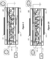
- FIG. 1 illustrates a first example of the use of PDLC in an RF/microwave device, in this example an antenna 100.
- the antenna 100 has a radiating patch 105, generally in the form of a copper patch formed or adhered to dielectric 110.
- Dielectric 110 may be, e.g., Rogers ® circuit board material, glass, PET, Teflon, etc.
- a ground plane 115 is provided between the bottom of dielectric 110 and the PDLC layer 120.
- a coupling window 125 is formed in the ground plane and is used to couple RF energy between the radiating patch 105 and the signal line 140.
- the signal line is coupled to an output port, e.g., a coaxial F-connector.
- the RF signal is capacitively coupled between the signal line 140 and radiating patch 105, via the intervening dielectric layer formed by the PDLC layer 120.
- the ground plane 115, the PDLC layer 120, and the signal line 140 form a capacitor, the characteristics of which depends on the dielectric constant value of the PDLC layer 120.
- the PDLC layer 120 is formed by a top dielectric layer/film 122, a bottom dielectric layer/film 124, spacers 126, and liquid crystal microdomains 128 dispersed in polymer 129 forming a PDLC.
- a high LC to polymer ratio is utilized, wherein the LC/polymer includes at least 70%, and preferably at least 80%, LC by weight.
- no alignment film is provided, such that the liquid crystals (directors) inside the microdomains 128 are randomly oriented, as shown in the callout A. Surprisingly, such a structure has faster response time than an LC film having alignment layer.
- An electrode 135 is coupled via control line 137 to a controller 150, which applies an AC, a DC, or a square-wave DC potential to the electrode 135.
- a controller 150 applies an AC, a DC, or a square-wave DC potential to the electrode 135.
- an electric field (indicated by the broken-line arrow) is formed, which causes the liquid crystals inside each of microdomains 128 in the vicinity of the electrode 135 to rotate in an amount corresponding to the applied potential, as shown in the callout B. Consequently, the characteristics of the capacitor formed between the ground plane 115 and the signal line 140 changes. This can be used to control the RF signal traveling in the signal line 140, e.g., to cause a delay or phase shift in the signal.
- FIG. 1A illustrates a first example of the use of SLC in an RF/microwave device, in this example an antenna 100.
- the antenna 100 has a radiating patch 105, generally in the form of a copper patch formed or adhered to dielectric 110.
- Dielectric 110 may be, e.g., Rogers ® circuit board material, glass, PET, Teflon, etc.
- a ground plane 115 is provided between the bottom of dielectric 110 and the PDLC layer 120.
- a coupling window 125 is formed in the ground plane and is used to couple RF energy between the radiating patch 105 and the signal line 140.
- the signal line is coupled to an output port, e.g., a coaxial F-connector.
- RF signal is capacitively coupled between the signal line 140 and radiating patch 105, via the intervening dielectric layer formed by the SLC layer 120.
- the ground plane 115, the SLC layer 120, and the signal line 140 form a capacitor, the characteristics of which depends on the dielectric constant value of the SLC layer 120.
- the SLC layer 120 is formed by a top dielectric layer/film 122, a bottom dielectric layer/film 124, spacers 126, and liquid crystal microdomains 128 dispersed in polymer 129 forming a PDLC.
- a high LC to polymer ratio is utilized, wherein the LC/polymer includes at least 70%, and preferably at least 80%, LC by weight.
- the liquid crystals inside the liquid crystal microdomains 128 are aligned by use of shearing. Specifically, by applying a shearing force between the top and bottom films 122 and 124, the microdomains 128 elongates as illustrated in Figure 1A . Additionally, due to the shearing force the LC domains within the liquid crystal microdomains 128 are all aligned in the direction of the shear force, as shown in the callout C.
- An electrode 135 is coupled via control line 137 to a controller 150, which applies an AC, a DC, or a square-wave DC potential to the electrode 135.
- a controller 150 applies an AC, a DC, or a square-wave DC potential to the electrode 135.
- an electric field (indicated by the broken-line arrow) is formed, which causes the liquid crystal domains inside each of microdomains 128 in the vicinity of the electrode 135 to rotate in an amount corresponding to the applied potential, as shown in the callout D.
- the microdomains are illustrated as rotated in order to convey the concept that the LC domains inside each liquid crystal microdomains 128 are rotated, but in reality the microdomains do not rotate, only the LC inside the microdomains 128 rotate.
- the characteristics of the capacitor formed between the ground plane 115 and the signal line 140 changes.
- This can be used to control the RF signal traveling in the signal line 140, e.g., to cause a delay or phase shift in the signal.
- the liquid crystal microdomains 128 are shown generally as spheres and the domains within these spheres are randomly oriented.
- the liquid crystal microdomains 128 are illustrated as ovals - to indicate the stretching due to the shearing force.
- the ovals are shown rotated.
- the following embodiments disclosed below can be implemented using either PDLC or SLC. Therefore, as a shortcut the layer will be referred to as PDLC/SLC, and the oval drawing will be used.
- each Figure illustrates two possible embodiments, one using PDLC and one using SLC.
- an antenna comprising: a dielectric plate; at least one radiating patch provided on the dielectric plate; a ground plane having at least one window, wherein each radiating patch is aligned with one window; at least one signal line, wherein each signal line is configured for capacitively coupling RF signal to one radiating patch; and a polymer dispersed liquid crystal (PDLC) layer provided between the signal line and the ground plane and comprising a top dielectric film, a bottom dielectric film, a plurality of spacers provided between the top dielectric film and bottom dielectric film, a polymer layer provided between the top dielectric film and the bottom dielectric film, and a plurality of liquid crystal microdomains dispersed in the polymer layer.
- PDLC polymer dispersed liquid crystal
- the spacers may be made of, e.g., glass, PS (polystyrene), PE (polyethylene), PP (polypropylene), PMMA, Silica, Cellulose acetate, Zirconia, acrylic or epoxy, etc. Also, the polymer layer may be shear-stressed, thus forming an SLC layer.
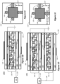
- Figures 1 and 1A illustrate examples wherein each patch has one signal line coupled to it.
- Figures 1B and 1C illustrate an embodiment wherein each radiating patch has two signal line coupled to it, wherein the two signal lines are orthogonal to each other.
- the elements of the embodiment of Figures 1B and 1C are the same as in the embodiments of Figures 1 or 1A , except that another dielectric layer 132 is provided below the first signal line 140, and an orthogonal second signal line 142 is provided below the second dielectric layer 132.
- one signal line can be used for transmission while the other signal line can be used for reception.
- both signal lines can be used to generate a circularly polarized signal by applying the control signal to electrode 135 in a manner that delays the signal in one of the signal lines with respect to the other.
- the embodiment of Figures 1B and 1C can be implemented using a plurality of radiating patches and corresponding signal and control lines.
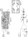
- FIGS 1D and 1E illustrate an embodiment wherein the transmission characteristics of each signal lines 135, 142, can be controlled independently.
- this embodiment utilizes multiple ground planes, each having windows aligned to couple RF signal between the radiating patch and the corresponding signal line.
- the arrangement can be implemented with multiple radiating patches, just as with the other embodiments.
- the beam can be steered in any direction in hemisphere space by the control signals applied to the multiple control lines, so as to independently control the delay applied to each signal line.
- the signal propagating in signal line 140 is controlled by applying control signal to electrode 135, thus rotating the LC microdomains in PDLC/SLC later 120, and the signal propagating in signal line 142 is controlled by applying control signal to electrode 138, thus rotating the LC microdomains in PDLC/SLC later 121.
- the signals are delayed by 90 0 with respect to each other, so as to generate circular polarization.
- Figures 1D and 1E provide an antenna having multiple PDLC/SLC layers and multiple ground planes, comprising: a top dielectric layer; a plurality of radiating patches provided over the top dielectric layer; a first liquid crystal layer positioned below the top dielectric layer; a first ground plane having a plurality of windows, each window aligned with one of the radiating patches; a plurality of first signal lines each terminating in alignment with one of the radiating patches; a plurality of first control lines, each aligned with one of the first signal lines; a second liquid crystal layer; a second ground plane having a plurality of windows, each aligned with one of the radiating patches; a plurality of second signal lines each terminating in alignment with one of the radiating patches; and a plurality of second control lines, each aligned with one of the first signal lines; wherein each of the first and second liquid crystal layers comprises a top dielectric, a bottom dielectric, a plurality of spacers provided between the top dielectric and bottom di
- the layers are arranged in the order, top to bottom: radiating patches, top dielectric layer, first ground plane, first (optionally stressed) liquid crystal layer, first control lines, first signal lines, second ground plane, second (optionally stressed) liquid crystal layer, second control lines and second signal lines.
- various intermediate dielectric layers are provided between the various signal lines, control lines and ground planes.
- Figure 1F illustrates an embodiment having multiple PDLC/SLC layers and multiple ground planes, but in a different order than that of Figure 1D .
- Figure 1F illustrates an embodiment similar to that of Figure 1D , except that the order of layers is different.
- the first signal line 140 is provided below the radiating patch 105, but above the first ground plane 115 and above the first PDLC/SLC layer 120.
- the first control line 135 may be provided above or below the first PDLC/SLC layer 120.
- the first ground plane 115 is provided below the first PDLC/SLC layer 120. While in this embodiment the first ground plane 115 has window 125, the window 125 is for coupling the signals to the second signal line 142 and is therefore aligned for the second signal line 142, not the first signal line 140.
- the signal for the first signal line 140 is coupled directly to the radiating patch 105 through the top dielectric 110.
- the window 125 in the first ground plane is aligned to couple the RF signal from the second signal line 142, since the second signal line 142 is below the first ground plane, but is above the second PDLC/SLC layer 121.
- the second ground plane 117 is provided below the second signal line 142 and, therefore, requires no windows.
- the second control line 138 may be provided below or above the second PDLC/SLC layer 121.
- an RF antenna having multiple ground planes and multiple variable dielectric layers comprising: a top dielectric layer; a plurality of radiating patches provided over the top dielectric; a first variable dielectric constant (VDC) layer; a first ground plane having a plurality of windows, each aligned with one of the radiating patches; a plurality of first signal lines, each terminating below one of the windows of the first ground plane; a plurality of first control lines, each configured to control liquid crystal domains of the first VDC layer in vicinity of one of the first signal lines; a second VDC layer provided below the first VDC layer; a second ground plane having a plurality of windows, each aligned with one of the radiating patches; a plurality of second signal lines, each terminating below one of the windows of the second ground plane; and a plurality of second control lines, each configured to control liquid crystal domains of the second VDC layer in vicinity of one of the second signal lines.
- VDC variable dielectric constant
- the two opposing dielectric substrates which encapsulate the liquid crystal cell can be made of any non-conduction material desired, whether transparent or opaque, since there are no optical considerations.
- the control electrodes can be made by, e.g., deposition such as evaporation, electroplating, electroless plating, etc., may be printed on using conducting ink or paste, etc. As shown in the embodiments disclosed herein, the control electrodes may be positioned on either side of the liquid crystal cell to generate the electrical field as required for the function of the RF device.
- control electrode and signal line materials can be a type of conduction material, specifically metal, such as gold (Au), silver (Ag), Titanium (Ti), Copper (Cu), Platinum (Pt), or other metals and/or metals layering or alloying.
- metal such as gold (Au), silver (Ag), Titanium (Ti), Copper (Cu), Platinum (Pt), or other metals and/or metals layering or alloying.
- spacers made of insulating material are placed to fix and maintain the desired cell gap.
- phase separation of the liquid crystal, into a non-cured (liquid phase) liquid crystal domains, and cured polymer (solid phase) is achieved via multiple possible ways, such as polymerization induced phase separation (PIPS), solvent-induced phase separation (SIPS), non-solvent induced phase separation (NIPS), thermally induced phase separation (TIPS), emulsion-based PDLC, and other methods as known on the art.
- PIPS polymerization induced phase separation
- SIPS solvent-induced phase separation
- NIPS non-solvent induced phase separation
- TIPS thermally induced phase separation
- emulsion-based PDLC emulsion-based PDLC
- the resulting structure is the PDLC layer.
- the liquid crystal domains are usually spherical or amorphous shape, and in these liquid crystal domains the liquid crystal directors themselves are oriented freely and without any general direction.
- Such PDLC film can be used in the disclosed embodiments.
- a shearing action is applied to the top or bottom substrates of the PDLC (any opposing movement of the top and bottom surfaces will generate such a shearing effect on the PDLC).
- the shearing may be done during or after the phase separation process.
- the SLC contains elongated liquid crystal domains, in the shearing direction.
- the film is now referred to a Stressed Liquid Crystal (SLC), and in the liquid crystal elongated domains themselves the liquid crystal directors are pointing in the same direction- the shearing direction. As it follows, the liquid crystal is thereby aligned throughout the bulk of the SLC, disregarding the SLC thickness and length.
- SLC Stressed Liquid Crystal
- the cell gap or height can be much higher than an LCD liquid crystal cell but still maintain LC domain alignment.
- phase separation stage is a critical parameter influencing the device ultimate performance. Initially, choosing the right polymer/pre-polymer and liquid crystal (or mixture thereof) must be so that there is as little as possible liquid crystal dissolved in the polymer, and that upon phase separation the highest degree of phase separation is achievable.
- the pre-polymer and LC mixture are heated to a temperature higher than the LC intrinsic temperature, so that the phase separation occurs when the LC is in its liquid form.
- the cell's temperature is reduced to Tn, and phase separation is continued until the entire pre-polymer is polymerized, and with as little as possible LC dissolved in the polymer matrix.
- the LC directors will be strongly aligned in the shearing direction, which is parallel to the cell's top and bottom substrates (or carrier films).
- the PDLC and/or SLC layers can be produced by roll to roll methods or using pre-cut thin polymer sheets. By maintaining the gap between the two enclosing carrier films, and polymerizing the three-layered film, a PDLC is formed in the same phase separation methods as described before. The PDLC can then be used in any of the disclosed embodiments. If the polymer used is not polymerized completely, or if it is thermoplastic in nature, a second stage of shearing or stretching (one or two directions) will produce the SLC layer, held between the two polymer films. Following that, the 3-layer polymer (two enclosing polymer films and the SLC in between) can be placed inside an RF device, without the need to conduct the entire chemical and mechanical process inside the RF device.
- the fabrication system can be adjusted such that one of the substrates is moving faster than the other, whereby shearing is carried out and the final polymerized three layered films comes out - sheared and aligned.
- FIG. 2 illustrates a roll-to-roll method of manufacturing the PDLC/SLC layer according to the embodiments of the invention.
- supply roll 201 provides a continuous strip of flexible insulating material 202, e.g., PET, polymer nanocomposites, Pyralux ® (Available from Du Pont), ECCOSTOCK ® low loss dielectrics (Available from Emerson & Cuming of Laird PLC, London, England), etc.
- supply roll 211 provides a continuous strip of insulating material 112, made of same or similar material as strip 202.
- the insulating strip 212 is passed through spacer station 205, wherein spacers are formed or deposited on the top surface of the insulating strip 212.
- PDLC station 208 the mixture of polymer precursor and liquid crystal microdomains is deposited onto the strip 202.
- the top and bottom films are then brought together and enter polymerization station 218 for phase separation and curing.
- Polymerization station 218 may operate according to any of the principles already mentioned, such as, PIPS, SIPS, NIPS, etc.
- the film now may be cut to size and each cut piece may be used to form an RF or microwave device, as disclosed herein. If an SLC is desired, then the cut piece may be transferred to a shearing station to impart the shear force to each cut piece individually.
- the shear force can be imparted prior to cutting the film by shear station 220.
- the supply of film can be halted, e.g., using clamps or vise 222, while one of the top or bottom films is still being pulled, e.g., by roller 224, thus creating relative shearing motion between the top and bottom films.
- the film may be cut to size.
- peeling station 225 is used to peel away the top or bottom, or both films, so as to draw a sheared and polymerized PDLC/SLC layer, which can then be cut to size.
- the layer than contains only a fully polymerized film, which is composed of the LC and surrounding polymer matrix only.
- Figure 1G illustrates an embodiment wherein the top and bottom carrier films are removed from the PDLC after the curing and shearing.
- the embodiment of Figure 1G is similar to that of Figure 1 , except that carrier dielectric films 122 and 124 are not used.
- the carrier dielectric films are removed and the neighboring metal layers directly contact the polymerized material 129.
- metal layers ground plane 115 and the control lines 135 are in direct physical contact with the polymerized material 129.
- the ground plane 115 and/or the control lines 135 may be formed directly on or adhered to the polymerized material 129.
- the same implementation can be done in any of the other embodiments disclosed herein.
- FIG. 1G Another feature illustrated in Figure 1G that may be implemented using any of the other embodiments disclosed herein is having multiple radiating patches, although only two 105 and 105a are shown in Figure 1G .
- the signal of each radiating patch is fed independently using signal lines 140 and 140a, via corresponding windows 125 and 125a.
- the dielectric constant for each signal line is controlled independently by corresponding control lines 135 and 135a.
- the dielectric for each signal line can be controlled independently, thereby introducing different delay to each line, thus steering or scanning the beam.
- Figure 1H illustrates yet another embodiment, which may be implemented using either PDLC or SLC.
- the arrangement of Figure 1H differs from the embodiment of Figure 1 , in that a meandering delay line 136 is connected to the radiating patch 105 using a contact via 137.
- the delay line ohmically couples the RF/microwave signal to the radiating patch through the contact via 137.
- the signal is then capacitively coupled to the signal line through the window 125 in the ground plane 115.
- the PDLC or SLC layer is provided between the meandering delay line and the ground plane.
- Figure 1I illustrates a top view of a 2x2 array antenna which utilizes the construction of Figure 1H , which better illustrates the meandering delay line 136 and the location of the window 125 in the ground plane.
- control signal is applied to the meandering delay lines, so as to control the orientation of the liquid crystals below the delay line.
- the control signal may be applied to the radiating patch 105.
- the radiating patch since the radiating patch is ohmically connected to the delay line through the contact via, the control signal is distributed to the delay line as well.
- an antenna comprising: a top dielectric plate; a plurality of radiating patches provided over the dielectric plate; a plurality of meandering delay lines provided below the dielectric plate; a plurality of contact vias, each connecting one of the meandering delay line to one of the radiating patches; a VDC layer provided below the plurality of meandering delay lines; a ground plane provide below the VDC layer and having a plurality of windows, each window aligned below one of the delay lines; and a plurality of signal lines, each aligned below on of the windows; wherein the VDC plate comprises one of a PDLC or an SLC.
Landscapes
- Physics & Mathematics (AREA)
- Electromagnetism (AREA)
- Waveguide Aerials (AREA)
- Variable-Direction Aerials And Aerial Arrays (AREA)
- Position Fixing By Use Of Radio Waves (AREA)
Claims (15)
- Antenne (100) umfassend:eine Schicht mit variabler Dielektrizitätskonstante, VDC;eine Vielzahl von strahlenden Patches (105), die über der VDC-Schicht vorgesehen sind;eine Vielzahl von Signalleitungen (140), die jeweils in Ausrichtung unter einem der strahlenden Patches enden;eine Vielzahl von Steuerleitungen (137), die jeweils mit einer der Signalleitungen korrespondieren;eine Grundplatte (115);wobei die VDC-Schicht eine polymerdispergierte Flüssigkristallschicht, PDLC, (120), einen oberen dielektrischen Film (122) und einen unteren dielektrischen Film (124) umfasst, wobei die PDLC-Schicht in einem polymerisierten und gescherten Zustand ist.
- Antenne nach Anspruch 1, wobei die Grundplatte eine Vielzahl von Fenstern (125) umfasst, wobei jedes Fenster in einer direkten Sichtlinie zwischen einem der strahlenden Patches und einer Korrespondierenden von den Signalleitung ausgerichtet ist.
- Antenne nach Anspruch 1, wobei die VDC-Schicht ferner Abstandshalter (126) umfasst, die zwischen dem oberen dielektrischen Film und dem unteren dielektrischen Film verteilt sind, und wobei die PDLC zwischen den Abstandshaltern dispergiert ist, insbesondere wobei die Signalleitung über dem oberen dielektrischen Film vorgesehen ist und die Masseebene unter dem unteren dielektrischen Film vorgesehen ist.
- Antenne nach Anspruch 1, wobei:die VDC-Schicht ferner Abstandshalter (126) umfasst, die zwischen der oberen dielektrischen Schicht und der unteren dielektrischen Schicht verteilt sind, und wobei die PDLC zwischen den Abstandshaltern dispergiert ist;die Signalleitung oberhalb der oberen dielektrischen Schicht vorgesehen ist; unddie Steuerleitung unterhalb des unteren dielektrischen Films vorgesehen ist.
- Antenne nach Anspruch 1, wobei:die VDC-Schicht ferner Abstandshalter (126) umfasst, die zwischen der oberen dielektrischen Schicht und der unteren dielektrischen Schicht verteilt sind, und wobei die PDLC zwischen den Abstandshaltern dispergiert ist;die Signalleitung unterhalb des unteren dielektrischen Films vorgesehen ist; unddie Masseebene oberhalb des oberen dielektrischen Films vorgesehen ist und eine Vielzahl von Fenstern (125) umfasst, wobei jedes Fenster in einer direkten Sichtlinie zwischen einem der strahlenden Patches und einer Korrespondierenden von den Signalleitungen ausgerichtet ist.
- Antenne nach Anspruch 1, ferner umfassend eine Vielzahl von orthogonalen Signalleitungen, die jeweils in Ausrichtung unter einem der strahlenden Patches und in einer orthogonalen Richtung zu einer der Vielzahl von Signalleitungen enden.
- Antenne nach Anspruch 6 ferner umfassend eine zweite Grundplatte (117).
- Antenne nach Anspruch 7, wobei die zweite Masseebene eine Vielzahl von Fenstern (125) umfasst, die jeweils in einer direkten Sichtlinie zwischen einem der strahlenden Patches und einer Korrespondierenden von den orthogonalen Signalleitungen ausgerichtet sind.
- Antenne nach Anspruch 6, ferner umfassend eine Vielzahl von zweiten Steuerleitungen (138), die jeweils mit einer der orthogonalen Signalleitungen korrespondieren.
- Antenne nach Anspruch 6, ferner umfassend eine zweite VDC-Schicht, die zwischen der Vielzahl von Signalleitungen und der Vielzahl von orthogonalen Signalleitungen angeordnet ist.
- Antenne nach Anspruch 1, wobei die VDC-Schicht ferner eine Vielzahl von Abstandshaltern (126) zwischen dem oberen Film und dem unteren Film umfasst, und wobei die PDLC zwischen den Abstandshaltern (126) dispergiert ist.
- Antenne nach Anspruch 1, ferner umfassend:eine Vielzahl von mäandernden Verzögerungsleitungen (136), die jeweils mit einer der strahlenden Patches verbunden sind;wobei die Grundplatte eine Vielzahl von Fenstern umfasst, wobei jedes Fenster zwischen einer der mäandernden Verzögerungsleitungen und einer Korrespondierenden der Signalleitung ausgerichtet ist.
- Antenne nach Anspruch 12, wobei jede der Steuerleitungen mit einer der mäandernden Verzögerungsleitungen verbunden ist.
- Antenne nach Anspruch 12, ferner umfassend: eine Vielzahl von Kontaktdurchlässen (137), die jeweils eine der mäandernden Verzögerungsleitungen mit einer der strahlenden Patches verbinden.
- Antenne nach Anspruch 14, wobei jede Verzögerungsleitung so konfiguriert ist, dass sie ein HF-/Mikrowellensignal über den Kontaktdurchlass ohmsch an ein strahlendes Patch koppelt und dass sie das HF-/Mikrowellensignal über das Fenster in der Grundplatte kapazitiv an eine Signalleitung koppelt.
Applications Claiming Priority (2)
| Application Number | Priority Date | Filing Date | Title |
|---|---|---|---|
| US201762574680P | 2017-10-19 | 2017-10-19 | |
| PCT/US2018/056793 WO2019079774A1 (en) | 2017-10-19 | 2018-10-19 | DISPERSED STATE ALIGNMENT PHASE MODULATOR DEVICE / POLYMER SHEAR |
Publications (3)
| Publication Number | Publication Date |
|---|---|
| EP3698435A1 EP3698435A1 (de) | 2020-08-26 |
| EP3698435A4 EP3698435A4 (de) | 2021-11-17 |
| EP3698435B1 true EP3698435B1 (de) | 2023-11-22 |
Family
ID=66170180
Family Applications (1)
| Application Number | Title | Priority Date | Filing Date |
|---|---|---|---|
| EP18868731.3A Active EP3698435B1 (de) | 2017-10-19 | 2018-10-19 | Polymerdispergierte/scherausgerichtete phasenmodulatorvorrichtung |
Country Status (7)
| Country | Link |
|---|---|
| US (1) | US11011854B2 (de) |
| EP (1) | EP3698435B1 (de) |
| JP (1) | JP7441471B2 (de) |
| KR (1) | KR102685713B1 (de) |
| CN (1) | CN111247693B (de) |
| CA (1) | CA3077700A1 (de) |
| WO (1) | WO2019079774A1 (de) |
Families Citing this family (12)
| Publication number | Priority date | Publication date | Assignee | Title |
|---|---|---|---|---|
| CN108493592B (zh) * | 2018-05-03 | 2019-12-20 | 京东方科技集团股份有限公司 | 微带天线及其制备方法和电子设备 |
| CN108803165A (zh) * | 2018-06-08 | 2018-11-13 | 京东方科技集团股份有限公司 | 一种液晶天线及其驱动方法、通讯设备 |
| JP7169914B2 (ja) * | 2019-03-15 | 2022-11-11 | 株式会社ジャパンディスプレイ | アンテナ装置及びフェーズドアレイアンテナ装置 |
| KR102670834B1 (ko) * | 2019-07-25 | 2024-05-29 | 엘지디스플레이 주식회사 | 액정을 포함하는 평판 안테나 |
| CN110534881B (zh) * | 2019-09-25 | 2021-01-22 | 京东方科技集团股份有限公司 | 液晶天线及其制作方法 |
| JP7623954B2 (ja) * | 2019-12-03 | 2025-01-29 | クラレ・ヨーロップ・ゲーエムベーハー | 積層体、ならびにアンテナシステムおよびその製造方法 |
| CN115053397B (zh) | 2021-01-08 | 2023-10-27 | 京东方科技集团股份有限公司 | 移相器及天线 |
| JP7589093B2 (ja) * | 2021-03-31 | 2024-11-25 | 株式会社ジャパンディスプレイ | 電波反射板 |
| US12438281B2 (en) * | 2021-11-19 | 2025-10-07 | Sderotech, Inc. | Variable dielectric based antenna with improved response time |
| EP4649551A1 (de) * | 2023-02-17 | 2025-11-19 | Carillon Technologies Management Corporation | Gruppenantenne |
| US20250226584A1 (en) * | 2023-07-11 | 2025-07-10 | Beijing Boe Technology Development Co., Ltd. | Antenna |
| CN119987065A (zh) * | 2025-03-21 | 2025-05-13 | 江苏科技大学 | 一种快速响应液晶光学相控阵器件 |
Family Cites Families (51)
| Publication number | Priority date | Publication date | Assignee | Title |
|---|---|---|---|---|
| US4937585A (en) * | 1987-09-09 | 1990-06-26 | Phasar Corporation | Microwave circuit module, such as an antenna, and method of making same |
| JP3506405B2 (ja) * | 1996-09-04 | 2004-03-15 | 日本電信電話株式会社 | 光学素子及び表示装置 |
| US6317248B1 (en) * | 1998-07-02 | 2001-11-13 | Donnelly Corporation | Busbars for electrically powered cells |
| JP3552971B2 (ja) | 1998-12-14 | 2004-08-11 | 松下電器産業株式会社 | アクティブフェイズドアレイアンテナ |
| JP3874964B2 (ja) | 1999-04-28 | 2007-01-31 | 日本放送協会 | 可変移相器 |
| JP2000341027A (ja) | 1999-05-27 | 2000-12-08 | Nippon Hoso Kyokai <Nhk> | パッチアンテナ装置 |
| JP2001083493A (ja) | 1999-09-16 | 2001-03-30 | Idemitsu Kosan Co Ltd | 液晶素子 |
| JP3535423B2 (ja) | 1999-10-18 | 2004-06-07 | 三菱電機株式会社 | レドーム |
| JP3411539B2 (ja) * | 2000-03-06 | 2003-06-03 | 株式会社日立製作所 | プラズマ処理装置及びプラズマ処理方法 |
| JP4070428B2 (ja) | 2001-07-04 | 2008-04-02 | 日本放送協会 | 周波数可変フィルタ |
| JP2004023228A (ja) | 2002-06-13 | 2004-01-22 | Matsushita Electric Ind Co Ltd | アンテナ制御装置、及びフェイズドアレイアンテナ |
| US7595850B2 (en) | 2003-02-11 | 2009-09-29 | Kent State University | Stressed liquid crystals materials for light modulation |
| US6982671B2 (en) * | 2003-02-25 | 2006-01-03 | Harris Corporation | Slot fed microstrip antenna having enhanced slot electromagnetic coupling |
| US8368596B2 (en) * | 2004-09-24 | 2013-02-05 | Viasat, Inc. | Planar antenna for mobile satellite applications |
| US20090278744A1 (en) | 2005-10-11 | 2009-11-12 | Panasonic Corporation | Phased array antenna |
| US7466269B2 (en) * | 2006-05-24 | 2008-12-16 | Wavebender, Inc. | Variable dielectric constant-based antenna and array |
| CN101479887A (zh) * | 2006-05-24 | 2009-07-08 | 韦夫班德尔公司 | 集成波导管天线和阵列 |
| SG189891A1 (en) | 2010-10-15 | 2013-06-28 | Searete Llc | Surface scattering antennas |
| DE102011056141A1 (de) * | 2010-12-20 | 2012-06-21 | Samsung Electronics Co., Ltd. | Negativspannungsgenerator, Dekoder, nicht-flüchtige Speichervorrichtung und Speichersystem, das eine negative Spannung verwendet |
| EP2575211B1 (de) | 2011-09-27 | 2014-11-05 | Technische Universität Darmstadt | Elektronisch steuerbare Planarphasen-Arrayantenne |
| JP6152114B2 (ja) * | 2011-10-31 | 2017-06-21 | ティコナ・エルエルシー | レーザーダイレクトストラクチャード基板を形成する際に使用するための熱可塑性組成物 |
| CN103576399B (zh) * | 2013-09-26 | 2016-06-01 | 西安空间无线电技术研究所 | 一种液晶光学相控阵天线实现方法 |
| US9923271B2 (en) * | 2013-10-21 | 2018-03-20 | Elwha Llc | Antenna system having at least two apertures facilitating reduction of interfering signals |
| WO2016026055A1 (en) * | 2014-08-22 | 2016-02-25 | UNIVERSITé LAVAL | Lc modulator devices based on non-uniform electrode structures |
| US20160093600A1 (en) * | 2014-09-25 | 2016-03-31 | X-Celeprint Limited | Compound micro-assembly strategies and devices |
| ES2755650T3 (es) * | 2014-10-17 | 2020-04-23 | Synoste Oy | Dispositivo con una antena receptora y sistema de transferencia de potencia relacionado |
| US9720265B2 (en) * | 2014-12-30 | 2017-08-01 | Allen Howard Engel | Manufacturing methods to shear liquid crystal |
| JP2016127481A (ja) * | 2015-01-06 | 2016-07-11 | 株式会社東芝 | 偏波共用アンテナ |
| US10312601B2 (en) * | 2015-01-12 | 2019-06-04 | Huawei Technologies Co., Ltd. | Combination antenna element and antenna array |
| US10128571B2 (en) * | 2015-02-13 | 2018-11-13 | Kymeta Corporation | Counter electrode device, system and method for varying the permittivity of a liquid crystal device |
| JP6517629B2 (ja) * | 2015-08-20 | 2019-05-22 | 株式会社東芝 | 平面型アンテナ装置 |
| WO2017115672A1 (ja) * | 2015-12-28 | 2017-07-06 | シャープ株式会社 | 走査アンテナおよびその製造方法 |
| CN107408759B (zh) | 2016-01-29 | 2018-11-09 | 夏普株式会社 | 扫描天线 |
| JP6554224B2 (ja) * | 2016-02-16 | 2019-07-31 | シャープ株式会社 | 走査アンテナ |
| CN105896082A (zh) * | 2016-02-23 | 2016-08-24 | 电子科技大学 | 一种基于液晶材料的频率和方向图可重构天线 |
| WO2017155084A1 (ja) * | 2016-03-11 | 2017-09-14 | シャープ株式会社 | 走査アンテナならびに走査アンテナの検査方法 |
| US10374324B2 (en) * | 2016-04-15 | 2019-08-06 | Kymeta Corporation | Antenna having MEMS-tuned RF resonators |
| CN106154603B (zh) * | 2016-07-29 | 2019-12-06 | 合肥工业大学 | 一种液晶移相单元及其构成的相控天线 |
| US10320070B2 (en) * | 2016-09-01 | 2019-06-11 | Wafer Llc | Variable dielectric constant antenna having split ground electrode |
| US10199710B2 (en) | 2016-09-01 | 2019-02-05 | Wafer Llc | Variable dielectric constant-based devices |
| US10326205B2 (en) * | 2016-09-01 | 2019-06-18 | Wafer Llc | Multi-layered software defined antenna and method of manufacture |
| US10686257B2 (en) * | 2016-09-01 | 2020-06-16 | Wafer Llc | Method of manufacturing software controlled antenna |
| JP7061810B2 (ja) * | 2016-12-07 | 2022-05-02 | ウェハー エルエルシー | 低損失電送機構及びそれを使用するアンテナ |
| US10361485B2 (en) * | 2017-08-04 | 2019-07-23 | Raytheon Company | Tripole current loop radiating element with integrated circularly polarized feed |
| US10705391B2 (en) * | 2017-08-30 | 2020-07-07 | Wafer Llc | Multi-state control of liquid crystals |
| WO2019089634A1 (en) * | 2017-10-30 | 2019-05-09 | Wafer, Llc | Multi-layer liquid crystal phase modulator |
| US10511096B2 (en) * | 2018-05-01 | 2019-12-17 | Wafer Llc | Low cost dielectric for electrical transmission and antenna using same |
| CN113227841B (zh) * | 2018-08-02 | 2025-11-28 | 韦弗有限责任公司 | 带有方波信号转向的天线阵列 |
| US11271300B2 (en) * | 2018-08-24 | 2022-03-08 | Searete Llc | Cavity-backed antenna array with distributed signal amplifiers for transmission of a high-power beam |
| US11355841B2 (en) * | 2018-08-24 | 2022-06-07 | Searete Llc | Waveguide-backed antenna array with distributed signal amplifiers for transmission of a high-power beam |
| CN112018518B (zh) * | 2019-05-29 | 2025-05-16 | 富泰华工业(深圳)有限公司 | 天线阵列及具有所述天线阵列的液晶显示器 |
-
2018
- 2018-10-19 EP EP18868731.3A patent/EP3698435B1/de active Active
- 2018-10-19 WO PCT/US2018/056793 patent/WO2019079774A1/en not_active Ceased
- 2018-10-19 KR KR1020207012023A patent/KR102685713B1/ko active Active
- 2018-10-19 CN CN201880068116.5A patent/CN111247693B/zh active Active
- 2018-10-19 US US16/166,009 patent/US11011854B2/en active Active
- 2018-10-19 CA CA3077700A patent/CA3077700A1/en active Pending
- 2018-10-19 JP JP2020521907A patent/JP7441471B2/ja active Active
Also Published As
| Publication number | Publication date |
|---|---|
| WO2019079774A4 (en) | 2019-06-13 |
| EP3698435A1 (de) | 2020-08-26 |
| CN111247693B (zh) | 2022-11-22 |
| CA3077700A1 (en) | 2019-04-25 |
| CN111247693A (zh) | 2020-06-05 |
| WO2019079774A1 (en) | 2019-04-25 |
| US11011854B2 (en) | 2021-05-18 |
| KR20200103627A (ko) | 2020-09-02 |
| JP2021500799A (ja) | 2021-01-07 |
| JP7441471B2 (ja) | 2024-03-01 |
| KR102685713B1 (ko) | 2024-07-16 |
| US20190123454A1 (en) | 2019-04-25 |
| EP3698435A4 (de) | 2021-11-17 |
Similar Documents
| Publication | Publication Date | Title |
|---|---|---|
| EP3698435B1 (de) | Polymerdispergierte/scherausgerichtete phasenmodulatorvorrichtung | |
| US10862219B2 (en) | Multi-layer liquid crystal phase modulator | |
| EP3830605B1 (de) | Antennenanordnung mit rechtecksignallenkung | |
| JP6695933B2 (ja) | 表面散乱アンテナの改善 | |
| CN107994302B (zh) | 液晶移相器及其工作方法 | |
| EP3656020B1 (de) | Antenne mit variabler dielektrischer konstante mit geteilter masseelektrode | |
| Ma et al. | Liquid crystals for advanced smart devices with microwave and millimeter‐wave applications: recent progress for next‐generation communications | |
| US9923271B2 (en) | Antenna system having at least two apertures facilitating reduction of interfering signals | |
| CN110085985B (zh) | 液晶盒及扫描天线 | |
| EP3425725B1 (de) | Bedienfeld und strahlungsvorrichtung damit | |
| US10770486B2 (en) | Method of producing liquid crystal cell, and liquid crystal cell | |
| US20230295509A1 (en) | Steerable antenna and method for heating and/or tempering of a steerable antenna | |
| Haneda et al. | Fabrication of LC-polymer films separating thick LC layer for reflect arrays | |
| JP2005244458A (ja) | 電波レンズ | |
| Mueller et al. | Liquid crystal based electronically steerable 4× 4 antenna array with single horn feed at Ka-Band | |
| Du et al. | A High Gain and Two-Dimensional Beam Scanning Liquid Crystal Phased Antenna Array | |
| Kim et al. | Binary-biasing strategy for achieving phase-state-independent high-speed response in liquid crystal phase shifters | |
| Karabey et al. | Stable satellite link by liquid crystal based phased array antennas | |
| Al-Duhni et al. | RIS with Nanomaterials for FutureG Applications | |
| CN113328260A (zh) | 基于高分子材料掺杂的电磁波极化调控材料及其应用 |
Legal Events
| Date | Code | Title | Description |
|---|---|---|---|
| STAA | Information on the status of an ep patent application or granted ep patent |
Free format text: STATUS: THE INTERNATIONAL PUBLICATION HAS BEEN MADE |
|
| PUAI | Public reference made under article 153(3) epc to a published international application that has entered the european phase |
Free format text: ORIGINAL CODE: 0009012 |
|
| STAA | Information on the status of an ep patent application or granted ep patent |
Free format text: STATUS: REQUEST FOR EXAMINATION WAS MADE |
|
| 17P | Request for examination filed |
Effective date: 20200513 |
|
| AK | Designated contracting states |
Kind code of ref document: A1 Designated state(s): AL AT BE BG CH CY CZ DE DK EE ES FI FR GB GR HR HU IE IS IT LI LT LU LV MC MK MT NL NO PL PT RO RS SE SI SK SM TR |
|
| AX | Request for extension of the european patent |
Extension state: BA ME |
|
| DAV | Request for validation of the european patent (deleted) | ||
| DAX | Request for extension of the european patent (deleted) | ||
| A4 | Supplementary search report drawn up and despatched |
Effective date: 20211020 |
|
| RIC1 | Information provided on ipc code assigned before grant |
Ipc: H01Q 21/06 20060101ALI20211014BHEP Ipc: H01P 3/00 20060101ALI20211014BHEP Ipc: H01Q 3/44 20060101ALI20211014BHEP Ipc: H01Q 9/04 20060101ALI20211014BHEP Ipc: H01Q 3/36 20060101AFI20211014BHEP |
|
| GRAP | Despatch of communication of intention to grant a patent |
Free format text: ORIGINAL CODE: EPIDOSNIGR1 |
|
| STAA | Information on the status of an ep patent application or granted ep patent |
Free format text: STATUS: GRANT OF PATENT IS INTENDED |
|
| RIC1 | Information provided on ipc code assigned before grant |
Ipc: H01Q 21/06 20060101ALI20230504BHEP Ipc: H01P 3/00 20060101ALI20230504BHEP Ipc: H01Q 3/44 20060101ALI20230504BHEP Ipc: H01Q 9/04 20060101ALI20230504BHEP Ipc: H01Q 3/36 20060101AFI20230504BHEP |
|
| INTG | Intention to grant announced |
Effective date: 20230607 |
|
| GRAS | Grant fee paid |
Free format text: ORIGINAL CODE: EPIDOSNIGR3 |
|
| GRAA | (expected) grant |
Free format text: ORIGINAL CODE: 0009210 |
|
| STAA | Information on the status of an ep patent application or granted ep patent |
Free format text: STATUS: THE PATENT HAS BEEN GRANTED |
|
| AK | Designated contracting states |
Kind code of ref document: B1 Designated state(s): AL AT BE BG CH CY CZ DE DK EE ES FI FR GB GR HR HU IE IS IT LI LT LU LV MC MK MT NL NO PL PT RO RS SE SI SK SM TR |
|
| REG | Reference to a national code |
Ref country code: GB Ref legal event code: FG4D |
|
| REG | Reference to a national code |
Ref country code: CH Ref legal event code: EP Ref country code: DE Ref legal event code: R096 Ref document number: 602018061612 Country of ref document: DE |
|
| REG | Reference to a national code |
Ref country code: IE Ref legal event code: FG4D |
|
| RAP2 | Party data changed (patent owner data changed or rights of a patent transferred) |
Owner name: SDEROTECH, INC. Owner name: WAFER LLC |
|
| P01 | Opt-out of the competence of the unified patent court (upc) registered |
Effective date: 20240105 |
|
| REG | Reference to a national code |
Ref country code: LT Ref legal event code: MG9D |
|
| REG | Reference to a national code |
Ref country code: NL Ref legal event code: MP Effective date: 20231122 |
|
| PG25 | Lapsed in a contracting state [announced via postgrant information from national office to epo] |
Ref country code: GR Free format text: LAPSE BECAUSE OF FAILURE TO SUBMIT A TRANSLATION OF THE DESCRIPTION OR TO PAY THE FEE WITHIN THE PRESCRIBED TIME-LIMIT Effective date: 20240223 |
|
| PG25 | Lapsed in a contracting state [announced via postgrant information from national office to epo] |
Ref country code: IS Free format text: LAPSE BECAUSE OF FAILURE TO SUBMIT A TRANSLATION OF THE DESCRIPTION OR TO PAY THE FEE WITHIN THE PRESCRIBED TIME-LIMIT Effective date: 20240322 |
|
| PG25 | Lapsed in a contracting state [announced via postgrant information from national office to epo] |
Ref country code: LT Free format text: LAPSE BECAUSE OF FAILURE TO SUBMIT A TRANSLATION OF THE DESCRIPTION OR TO PAY THE FEE WITHIN THE PRESCRIBED TIME-LIMIT Effective date: 20231122 |
|
| REG | Reference to a national code |
Ref country code: AT Ref legal event code: MK05 Ref document number: 1634718 Country of ref document: AT Kind code of ref document: T Effective date: 20231122 |
|
| PG25 | Lapsed in a contracting state [announced via postgrant information from national office to epo] |
Ref country code: NL Free format text: LAPSE BECAUSE OF FAILURE TO SUBMIT A TRANSLATION OF THE DESCRIPTION OR TO PAY THE FEE WITHIN THE PRESCRIBED TIME-LIMIT Effective date: 20231122 |
|
| PG25 | Lapsed in a contracting state [announced via postgrant information from national office to epo] |
Ref country code: AT Free format text: LAPSE BECAUSE OF FAILURE TO SUBMIT A TRANSLATION OF THE DESCRIPTION OR TO PAY THE FEE WITHIN THE PRESCRIBED TIME-LIMIT Effective date: 20231122 |
|
| PG25 | Lapsed in a contracting state [announced via postgrant information from national office to epo] |
Ref country code: ES Free format text: LAPSE BECAUSE OF FAILURE TO SUBMIT A TRANSLATION OF THE DESCRIPTION OR TO PAY THE FEE WITHIN THE PRESCRIBED TIME-LIMIT Effective date: 20231122 |
|
| PG25 | Lapsed in a contracting state [announced via postgrant information from national office to epo] |
Ref country code: NL Free format text: LAPSE BECAUSE OF FAILURE TO SUBMIT A TRANSLATION OF THE DESCRIPTION OR TO PAY THE FEE WITHIN THE PRESCRIBED TIME-LIMIT Effective date: 20231122 Ref country code: LT Free format text: LAPSE BECAUSE OF FAILURE TO SUBMIT A TRANSLATION OF THE DESCRIPTION OR TO PAY THE FEE WITHIN THE PRESCRIBED TIME-LIMIT Effective date: 20231122 Ref country code: IS Free format text: LAPSE BECAUSE OF FAILURE TO SUBMIT A TRANSLATION OF THE DESCRIPTION OR TO PAY THE FEE WITHIN THE PRESCRIBED TIME-LIMIT Effective date: 20240322 Ref country code: GR Free format text: LAPSE BECAUSE OF FAILURE TO SUBMIT A TRANSLATION OF THE DESCRIPTION OR TO PAY THE FEE WITHIN THE PRESCRIBED TIME-LIMIT Effective date: 20240223 Ref country code: ES Free format text: LAPSE BECAUSE OF FAILURE TO SUBMIT A TRANSLATION OF THE DESCRIPTION OR TO PAY THE FEE WITHIN THE PRESCRIBED TIME-LIMIT Effective date: 20231122 Ref country code: BG Free format text: LAPSE BECAUSE OF FAILURE TO SUBMIT A TRANSLATION OF THE DESCRIPTION OR TO PAY THE FEE WITHIN THE PRESCRIBED TIME-LIMIT Effective date: 20240222 Ref country code: AT Free format text: LAPSE BECAUSE OF FAILURE TO SUBMIT A TRANSLATION OF THE DESCRIPTION OR TO PAY THE FEE WITHIN THE PRESCRIBED TIME-LIMIT Effective date: 20231122 Ref country code: PT Free format text: LAPSE BECAUSE OF FAILURE TO SUBMIT A TRANSLATION OF THE DESCRIPTION OR TO PAY THE FEE WITHIN THE PRESCRIBED TIME-LIMIT Effective date: 20240322 |
|
| PG25 | Lapsed in a contracting state [announced via postgrant information from national office to epo] |
Ref country code: SE Free format text: LAPSE BECAUSE OF FAILURE TO SUBMIT A TRANSLATION OF THE DESCRIPTION OR TO PAY THE FEE WITHIN THE PRESCRIBED TIME-LIMIT Effective date: 20231122 Ref country code: RS Free format text: LAPSE BECAUSE OF FAILURE TO SUBMIT A TRANSLATION OF THE DESCRIPTION OR TO PAY THE FEE WITHIN THE PRESCRIBED TIME-LIMIT Effective date: 20231122 Ref country code: PL Free format text: LAPSE BECAUSE OF FAILURE TO SUBMIT A TRANSLATION OF THE DESCRIPTION OR TO PAY THE FEE WITHIN THE PRESCRIBED TIME-LIMIT Effective date: 20231122 Ref country code: NO Free format text: LAPSE BECAUSE OF FAILURE TO SUBMIT A TRANSLATION OF THE DESCRIPTION OR TO PAY THE FEE WITHIN THE PRESCRIBED TIME-LIMIT Effective date: 20240222 Ref country code: LV Free format text: LAPSE BECAUSE OF FAILURE TO SUBMIT A TRANSLATION OF THE DESCRIPTION OR TO PAY THE FEE WITHIN THE PRESCRIBED TIME-LIMIT Effective date: 20231122 Ref country code: HR Free format text: LAPSE BECAUSE OF FAILURE TO SUBMIT A TRANSLATION OF THE DESCRIPTION OR TO PAY THE FEE WITHIN THE PRESCRIBED TIME-LIMIT Effective date: 20231122 |
|
| PG25 | Lapsed in a contracting state [announced via postgrant information from national office to epo] |
Ref country code: DK Free format text: LAPSE BECAUSE OF FAILURE TO SUBMIT A TRANSLATION OF THE DESCRIPTION OR TO PAY THE FEE WITHIN THE PRESCRIBED TIME-LIMIT Effective date: 20231122 |
|
| PG25 | Lapsed in a contracting state [announced via postgrant information from national office to epo] |
Ref country code: CZ Free format text: LAPSE BECAUSE OF FAILURE TO SUBMIT A TRANSLATION OF THE DESCRIPTION OR TO PAY THE FEE WITHIN THE PRESCRIBED TIME-LIMIT Effective date: 20231122 |
|
| PG25 | Lapsed in a contracting state [announced via postgrant information from national office to epo] |
Ref country code: SK Free format text: LAPSE BECAUSE OF FAILURE TO SUBMIT A TRANSLATION OF THE DESCRIPTION OR TO PAY THE FEE WITHIN THE PRESCRIBED TIME-LIMIT Effective date: 20231122 |
|
| PG25 | Lapsed in a contracting state [announced via postgrant information from national office to epo] |
Ref country code: SM Free format text: LAPSE BECAUSE OF FAILURE TO SUBMIT A TRANSLATION OF THE DESCRIPTION OR TO PAY THE FEE WITHIN THE PRESCRIBED TIME-LIMIT Effective date: 20231122 Ref country code: SK Free format text: LAPSE BECAUSE OF FAILURE TO SUBMIT A TRANSLATION OF THE DESCRIPTION OR TO PAY THE FEE WITHIN THE PRESCRIBED TIME-LIMIT Effective date: 20231122 Ref country code: RO Free format text: LAPSE BECAUSE OF FAILURE TO SUBMIT A TRANSLATION OF THE DESCRIPTION OR TO PAY THE FEE WITHIN THE PRESCRIBED TIME-LIMIT Effective date: 20231122 Ref country code: IT Free format text: LAPSE BECAUSE OF FAILURE TO SUBMIT A TRANSLATION OF THE DESCRIPTION OR TO PAY THE FEE WITHIN THE PRESCRIBED TIME-LIMIT Effective date: 20231122 Ref country code: EE Free format text: LAPSE BECAUSE OF FAILURE TO SUBMIT A TRANSLATION OF THE DESCRIPTION OR TO PAY THE FEE WITHIN THE PRESCRIBED TIME-LIMIT Effective date: 20231122 Ref country code: DK Free format text: LAPSE BECAUSE OF FAILURE TO SUBMIT A TRANSLATION OF THE DESCRIPTION OR TO PAY THE FEE WITHIN THE PRESCRIBED TIME-LIMIT Effective date: 20231122 Ref country code: CZ Free format text: LAPSE BECAUSE OF FAILURE TO SUBMIT A TRANSLATION OF THE DESCRIPTION OR TO PAY THE FEE WITHIN THE PRESCRIBED TIME-LIMIT Effective date: 20231122 |
|
| REG | Reference to a national code |
Ref country code: DE Ref legal event code: R097 Ref document number: 602018061612 Country of ref document: DE |
|
| PLBE | No opposition filed within time limit |
Free format text: ORIGINAL CODE: 0009261 |
|
| STAA | Information on the status of an ep patent application or granted ep patent |
Free format text: STATUS: NO OPPOSITION FILED WITHIN TIME LIMIT |
|
| PG25 | Lapsed in a contracting state [announced via postgrant information from national office to epo] |
Ref country code: SI Free format text: LAPSE BECAUSE OF FAILURE TO SUBMIT A TRANSLATION OF THE DESCRIPTION OR TO PAY THE FEE WITHIN THE PRESCRIBED TIME-LIMIT Effective date: 20231122 |
|
| 26N | No opposition filed |
Effective date: 20240823 |
|
| PG25 | Lapsed in a contracting state [announced via postgrant information from national office to epo] |
Ref country code: SI Free format text: LAPSE BECAUSE OF FAILURE TO SUBMIT A TRANSLATION OF THE DESCRIPTION OR TO PAY THE FEE WITHIN THE PRESCRIBED TIME-LIMIT Effective date: 20231122 |
|
| REG | Reference to a national code |
Ref country code: CH Ref legal event code: PL |
|
| PG25 | Lapsed in a contracting state [announced via postgrant information from national office to epo] |
Ref country code: MC Free format text: LAPSE BECAUSE OF FAILURE TO SUBMIT A TRANSLATION OF THE DESCRIPTION OR TO PAY THE FEE WITHIN THE PRESCRIBED TIME-LIMIT Effective date: 20231122 |
|
| PG25 | Lapsed in a contracting state [announced via postgrant information from national office to epo] |
Ref country code: BE Free format text: LAPSE BECAUSE OF NON-PAYMENT OF DUE FEES Effective date: 20241031 Ref country code: LU Free format text: LAPSE BECAUSE OF NON-PAYMENT OF DUE FEES Effective date: 20241019 |
|
| PG25 | Lapsed in a contracting state [announced via postgrant information from national office to epo] |
Ref country code: CH Free format text: LAPSE BECAUSE OF NON-PAYMENT OF DUE FEES Effective date: 20241031 |
|
| REG | Reference to a national code |
Ref country code: BE Ref legal event code: MM Effective date: 20241031 |
|
| PG25 | Lapsed in a contracting state [announced via postgrant information from national office to epo] |
Ref country code: FI Free format text: LAPSE BECAUSE OF FAILURE TO SUBMIT A TRANSLATION OF THE DESCRIPTION OR TO PAY THE FEE WITHIN THE PRESCRIBED TIME-LIMIT Effective date: 20231122 |
|
| PGFP | Annual fee paid to national office [announced via postgrant information from national office to epo] |
Ref country code: GB Payment date: 20250828 Year of fee payment: 8 |
|
| PGFP | Annual fee paid to national office [announced via postgrant information from national office to epo] |
Ref country code: FR Payment date: 20250821 Year of fee payment: 8 |
|
| PGFP | Annual fee paid to national office [announced via postgrant information from national office to epo] |
Ref country code: IE Payment date: 20250827 Year of fee payment: 8 |
|
| PGFP | Annual fee paid to national office [announced via postgrant information from national office to epo] |
Ref country code: DE Payment date: 20250827 Year of fee payment: 8 |
|
| PG25 | Lapsed in a contracting state [announced via postgrant information from national office to epo] |
Ref country code: CY Free format text: LAPSE BECAUSE OF FAILURE TO SUBMIT A TRANSLATION OF THE DESCRIPTION OR TO PAY THE FEE WITHIN THE PRESCRIBED TIME-LIMIT; INVALID AB INITIO Effective date: 20181019 |