EP3696138A1 - Method of stress relief in anti-reflective coated cap wafers for wafer level packaged infrared focal plane arrays - Google Patents
Method of stress relief in anti-reflective coated cap wafers for wafer level packaged infrared focal plane arrays Download PDFInfo
- Publication number
- EP3696138A1 EP3696138A1 EP20163773.3A EP20163773A EP3696138A1 EP 3696138 A1 EP3696138 A1 EP 3696138A1 EP 20163773 A EP20163773 A EP 20163773A EP 3696138 A1 EP3696138 A1 EP 3696138A1
- Authority
- EP
- European Patent Office
- Prior art keywords
- wafer
- cap wafer
- reflective coating
- discontinuous layer
- coating material
- Prior art date
- Legal status (The legal status is an assumption and is not a legal conclusion. Google has not performed a legal analysis and makes no representation as to the accuracy of the status listed.)
- Withdrawn
Links
- 238000000034 method Methods 0.000 title claims abstract description 45
- 230000003667 anti-reflective effect Effects 0.000 title description 34
- 238000003491 array Methods 0.000 title description 2
- 235000012431 wafers Nutrition 0.000 title 2
- 238000000576 coating method Methods 0.000 claims abstract description 75
- 239000011248 coating agent Substances 0.000 claims abstract description 68
- 239000000463 material Substances 0.000 claims abstract description 51
- 239000006117 anti-reflective coating Substances 0.000 claims abstract description 37
- 238000000151 deposition Methods 0.000 claims abstract description 16
- 238000001228 spectrum Methods 0.000 claims description 3
- 230000035882 stress Effects 0.000 description 14
- 239000010408 film Substances 0.000 description 8
- 239000000758 substrate Substances 0.000 description 8
- 230000008021 deposition Effects 0.000 description 6
- 238000010586 diagram Methods 0.000 description 6
- 230000005855 radiation Effects 0.000 description 6
- 239000010409 thin film Substances 0.000 description 6
- 238000007689 inspection Methods 0.000 description 5
- 238000004519 manufacturing process Methods 0.000 description 4
- 230000008569 process Effects 0.000 description 4
- 230000008646 thermal stress Effects 0.000 description 4
- 238000001429 visible spectrum Methods 0.000 description 4
- 238000010276 construction Methods 0.000 description 3
- 238000002329 infrared spectrum Methods 0.000 description 3
- 238000012545 processing Methods 0.000 description 3
- 230000004075 alteration Effects 0.000 description 2
- 230000008901 benefit Effects 0.000 description 2
- 230000008859 change Effects 0.000 description 2
- 239000003989 dielectric material Substances 0.000 description 2
- 238000005516 engineering process Methods 0.000 description 2
- 239000007789 gas Substances 0.000 description 2
- 230000006872 improvement Effects 0.000 description 2
- 238000012986 modification Methods 0.000 description 2
- 230000004048 modification Effects 0.000 description 2
- 230000003287 optical effect Effects 0.000 description 2
- 238000004806 packaging method and process Methods 0.000 description 2
- 239000004065 semiconductor Substances 0.000 description 2
- 229910001220 stainless steel Inorganic materials 0.000 description 2
- 239000010935 stainless steel Substances 0.000 description 2
- 229910052984 zinc sulfide Inorganic materials 0.000 description 2
- PFNQVRZLDWYSCW-UHFFFAOYSA-N (fluoren-9-ylideneamino) n-naphthalen-1-ylcarbamate Chemical compound C12=CC=CC=C2C2=CC=CC=C2C1=NOC(=O)NC1=CC=CC2=CC=CC=C12 PFNQVRZLDWYSCW-UHFFFAOYSA-N 0.000 description 1
- 239000005083 Zinc sulfide Substances 0.000 description 1
- 238000001816 cooling Methods 0.000 description 1
- 238000005520 cutting process Methods 0.000 description 1
- 230000001419 dependent effect Effects 0.000 description 1
- 230000000694 effects Effects 0.000 description 1
- 230000005670 electromagnetic radiation Effects 0.000 description 1
- 229910052732 germanium Inorganic materials 0.000 description 1
- GNPVGFCGXDBREM-UHFFFAOYSA-N germanium atom Chemical compound [Ge] GNPVGFCGXDBREM-UHFFFAOYSA-N 0.000 description 1
- 238000010438 heat treatment Methods 0.000 description 1
- 238000003384 imaging method Methods 0.000 description 1
- 238000011065 in-situ storage Methods 0.000 description 1
- 230000003993 interaction Effects 0.000 description 1
- 150000002500 ions Chemical class 0.000 description 1
- 229910000833 kovar Inorganic materials 0.000 description 1
- 230000000873 masking effect Effects 0.000 description 1
- 238000005259 measurement Methods 0.000 description 1
- 239000002184 metal Substances 0.000 description 1
- 229910052751 metal Inorganic materials 0.000 description 1
- 238000004377 microelectronic Methods 0.000 description 1
- 238000000386 microscopy Methods 0.000 description 1
- 238000012856 packing Methods 0.000 description 1
- 239000002245 particle Substances 0.000 description 1
- 238000005498 polishing Methods 0.000 description 1
- 229910052594 sapphire Inorganic materials 0.000 description 1
- 239000010980 sapphire Substances 0.000 description 1
- 230000011218 segmentation Effects 0.000 description 1
- 239000002210 silicon-based material Substances 0.000 description 1
- 229910000679 solder Inorganic materials 0.000 description 1
- 229910052950 sphalerite Inorganic materials 0.000 description 1
- 238000009461 vacuum packaging Methods 0.000 description 1
- DRDVZXDWVBGGMH-UHFFFAOYSA-N zinc;sulfide Chemical compound [S-2].[Zn+2] DRDVZXDWVBGGMH-UHFFFAOYSA-N 0.000 description 1
Images


Classifications
-
- B—PERFORMING OPERATIONS; TRANSPORTING
- B81—MICROSTRUCTURAL TECHNOLOGY
- B81C—PROCESSES OR APPARATUS SPECIALLY ADAPTED FOR THE MANUFACTURE OR TREATMENT OF MICROSTRUCTURAL DEVICES OR SYSTEMS
- B81C1/00—Manufacture or treatment of devices or systems in or on a substrate
- B81C1/00015—Manufacture or treatment of devices or systems in or on a substrate for manufacturing microsystems
- B81C1/00261—Processes for packaging MEMS devices
- B81C1/00325—Processes for packaging MEMS devices for reducing stress inside of the package structure
-
- B—PERFORMING OPERATIONS; TRANSPORTING
- B05—SPRAYING OR ATOMISING IN GENERAL; APPLYING FLUENT MATERIALS TO SURFACES, IN GENERAL
- B05D—PROCESSES FOR APPLYING FLUENT MATERIALS TO SURFACES, IN GENERAL
- B05D5/00—Processes for applying liquids or other fluent materials to surfaces to obtain special surface effects, finishes or structures
- B05D5/06—Processes for applying liquids or other fluent materials to surfaces to obtain special surface effects, finishes or structures to obtain multicolour or other optical effects
- B05D5/061—Special surface effect
-
- B—PERFORMING OPERATIONS; TRANSPORTING
- B81—MICROSTRUCTURAL TECHNOLOGY
- B81B—MICROSTRUCTURAL DEVICES OR SYSTEMS, e.g. MICROMECHANICAL DEVICES
- B81B7/00—Microstructural systems; Auxiliary parts of microstructural devices or systems
- B81B7/0032—Packages or encapsulation
- B81B7/0067—Packages or encapsulation for controlling the passage of optical signals through the package
-
- B—PERFORMING OPERATIONS; TRANSPORTING
- B81—MICROSTRUCTURAL TECHNOLOGY
- B81B—MICROSTRUCTURAL DEVICES OR SYSTEMS, e.g. MICROMECHANICAL DEVICES
- B81B2201/00—Specific applications of microelectromechanical systems
- B81B2201/02—Sensors
- B81B2201/0207—Bolometers
-
- B—PERFORMING OPERATIONS; TRANSPORTING
- B81—MICROSTRUCTURAL TECHNOLOGY
- B81C—PROCESSES OR APPARATUS SPECIALLY ADAPTED FOR THE MANUFACTURE OR TREATMENT OF MICROSTRUCTURAL DEVICES OR SYSTEMS
- B81C2203/00—Forming microstructural systems
- B81C2203/01—Packaging MEMS
- B81C2203/0118—Bonding a wafer on the substrate, i.e. where the cap consists of another wafer
Definitions
- MEMS Microelectromechanical systems
- the critical physical dimensions of MEMS devices can vary from well below one micrometer (micron) to several millimeters.
- the types of MEMS devices can vary from relatively simple structures lacking any moving elements, to extremely complex electromechanical systems with multiple moving elements that are under the control of integrated microelectronics.
- Non-limiting examples of MEMS devices include sensors and optical devices, such as single-band or multi-band detector focal plane arrays (FPAs) or microbolometers.
- FPA devices may include single-band or multi-band integrated FPAs (e.g., single band visible FPA devices, or integrated dual-band FPA devices that are capable of detecting both near infrared (IR) spectrum radiation and visible spectrum radiation).
- Microbolometers are often fabricated using integrated circuit fabrication techniques.
- the basic construction includes a substrate that includes an FPA that comprises a plurality of detector elements that correspond to respective pixels.
- the substrate contains an integrated circuit which is electrically coupled to the detector elements, and is commonly known as a read out integrated circuit (ROIC).
- ROIC read out integrated circuit
- microbolometers are generally placed in vacuum packages to provide an isolated environment for the device.
- the vacuum package provides an optimal environment for the sensing device, since the presence of gas may impede performance.
- the bolometer may be packaged in a specific atmosphere comprising one or more gases.
- aspects and embodiments relate generally to methods for reducing wafer bow, and more particularly, to reducing wafer bow induced by an anti-reflective coating on a cap wafer.
- a method of reducing wafer bow induced by an anti-reflective coating on a cap wafer comprises providing the cap wafer having a planar side and an opposing cavity side, the cavity side including at least one recessed region and a dividing region on either side of the at least one recessed region, positioning a first shadow mask having at least one opening therein over the planar side of the cap wafer, aligning the first shadow mask such that the at least one opening is positioned opposite the at least one recessed region, and depositing at least one layer of an anti-reflective coating material through the first shadow mask onto the planar side of the cap wafer to provide a discontinuous coating on the planar side.
- the discontinuous coating is dimensioned and configured such that a wafer bow induced by the anti-reflective coating is less than 30 microns for an 8 inch diameter cap wafer. In some aspects, the wafer bow is less than 20 microns.
- the at least one opening in the first shadow mask is dimensioned to extend appreciably beyond the at least one recessed region on the cap wafer.
- the at least one recessed region corresponds to the location of at least one micro-electromechanical system (MEMS) device on a corresponding device wafer.
- MEMS micro-electromechanical system
- the discontinuous coating corresponds to saw streets on the cap wafer.
- the method further comprises positioning a second shadow mask having at least one opening therein over the cavity side of the cap wafer and aligning the second shadow mask such that the at least one opening is positioned over the at least one recessed region.
- the method further comprises depositing at least one layer of an anti-reflective coating material through the at least one opening in the second shadow mask onto the cavity side of the cap wafer to provide a discontinuous coating on the cavity side.
- the discontinuous coating on the planar side is dimensioned and configured such that a wafer bow induced by the anti-reflective coating is less than 30 microns for an 8 inch diameter cap wafer.
- the discontinuous coating on the planar side is dimensioned and configured such that a wafer bow induced by the anti-reflective coating is in balance with a wafer bow induced by the anti-reflective coating on the cavity side.
- the method further comprises providing a device wafer onto which at least one MEMS device is formed.
- the method further comprises positioning the cap wafer over the device wafer such that the cavity side of the cap wafer is facing the at least one MEMS device, aligning the cap wafer to the device wafer such that the at least one recessed region is positioned over the at least one MEMS device, and bonding the cap wafer to the device wafer to create bonding structures.
- the method further comprises inspecting the bonding structures through inspection regions provided by the discontinuous coating on the planar side of the cap wafer.
- the inspection is performed using a charge-coupled device (CCD).
- CCD charge-coupled device
- aspects and embodiments are directed toward providing a method for reducing wafer bow induced by an anti-reflective coating.
- aspects and embodiments are directed to reducing wafer bow in a cap wafer.
- a cap wafer may be bonded to an ROIC device wafer, enclosing the sensor device (for example, one or more microbolometers) to provide a protected and sealed environment surrounding the sensor device.
- Fabrication of the cap wafer may include coating the cap wafer with an anti-reflective (AR) coating.
- AR anti-reflective
- the AR coating may be included on both sides of the cap wafer.
- the AR coating may be dimensioned differently on both sides of the wafer, which may induce internal stress in the cap wafer. The internal stress causes the cap wafer to bow or curve, which leads to multiple processing concerns. Accordingly, aspects and embodiments are directed to reducing or eliminating bow in the cap wafer by selectively applying the AR coating, as discussed in more detail below.
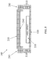
- FIG. 1 A fully packaged MEMS device comprising a sensor element is illustrated in FIG. 1 .
- the terms "micro-electromechanical system” and “MEMS” are used interchangeably, and may refer to any one of a variety of MEMS devices.
- the term “MEMS device” is used as a general term to refer to electromechanical devices, and is not intended to refer to any particular scale of electromechanical devices unless specifically noted otherwise.
- the MEMS device is an uncooled infrared bolometer FPA.
- a MEMS device such as an FPA, including a pixel array 110 formed on an ROIC wafer 120.
- the device may need to be packaged in a vacuum that includes a reliable hermetic seal and an integrated infrared (IR) window structure 130.
- the window 130 may include at least a portion of a cap wafer 140 that is transmissive to infrared radiation.
- this packaging may be performed at the wafer level.
- the cap wafer 140 for covering the sensor element is formed from a semiconductor wafer.
- the fixing of the cap wafer 140 to the ROIC wafer 120 may be performed after the sensor elements (e.g., pixel array 120) are formed on the ROIC wafer.
- a dicing process may be performed after the cap is fixed to the wafer to produce individual devices. An example of such an individual device is shown in FIG. 1 .
- the cap wafer 140 may be coated with an anti-reflective (AR) coating 150.
- Window areas are formed from recesses 160 that are etched into the cap wafer 140 and correspond with areas of the cap wafer that are covered with the AR coating 150.
- the recessed region 160 of the cap wafer 140 is positioned over the pixel array 110 and bonded to the ROIC wafer 120 using solder bonds 170, for example, to create an enclosed and sealed environment.
- the terms “lid wafer” and “cap wafer” are used interchangeably and refer to a wafer comprising at least one recess that is suitable for use with a device wafer comprising one or more devices, such as MEMS devices.
- the term “recess” refers to a structure that can be described as a cavity within the wafer material that does not actually extend through the wafer.
- the cap wafer 140 is attached to the device wafer 120 in such a way as to form a hermetically sealed environment within the recess 160 covering the pixel array 110.
- the recessed area 160 may include one or more layers of an optically transmissive material. In such a configuration, the cap wafer 140 provides an optically transmissive window 130 above the pixel array 110.
- AR coatings may include a thin layer of dielectric material, with a selected thickness so that interference effects in the coating cause the wave reflected from the top surface of the AR coating to be out of phase with the wave reflected from an underlying semiconductor surface. The out-of-phase reflected waves destructively interfere with one another, resulting in substantially zero net reflected energy.
- AR coating 150 may be any material that is suitable for the purposes of performing an anti-reflective function as described in the methods and systems disclosed herein.
- the AR coating may comprise germanium or ZnS.
- AR coating 150 may be an IR-transmitting material.
- the internal stress in the AR coating 150 may induce from about 60 to over 100 microns of bowing.
- the bowing may interfere with multiple processing steps. For example, the bowing may result in non-uniform polishing off of the AR coating on the cavity side (if a polish-off process is utilized), hinder proper alignment between the cap wafer and the device wafer, prevent complete thermal contact with heater chucks or other associated structure, and interfere with the wafer level bonding process.
- the discontinuous coating 230 may form a pattern, for example, where areas defined by one or more layers of coating material are separated from each other by areas that are not covered by coating material.
- the pattern of the discontinuous coating 230 corresponds to a pattern on the recesses of the cavity side 220 of the cap wafer 140, such that portions of the coatings on either side of the cap wafer overlie one another. This is illustrated in FIG. 2C .
- At least one of the coatings 230 and 240 may be AR coatings, as discussed above.
- FIG. 2C illustrates coatings 230 and 240 on both sides of the cap wafer 140, it is to be appreciated that in other embodiments the discontinuous coating 230 may be formed on the planar side 210 of the cap wafer without a coating on the cavity side 220.
- the discontinuous coating that corresponds to the at least one recessed region is dimensioned and configured so that the wafer bow induced by the coating is less than 30 microns for an 8 inch diameter cap wafer. According to a further embodiment, the wafer bow may be less than 20 microns.
- the method may further comprise a step 330 of depositing a coating material, such as an AR coating, in the recessed regions 160 on the cavity side 220 of the cap wafer 140, as is also shown in FIG. 2C and discussed above.
- deposition step 330 may also be accomplished using a shadow mask that is positioned over the cavity side 220 with openings aligned with the recesses 160. This is exemplified in step 325 of the figure.
- the deposition step 330 may occur without using a shadow mask.
- the coated surface on the cavity side may subsequently be polished off (referred to herein as polish-off) so that the AR material is present only in the recessed regions 160.
- the coating 240 may be applied to the cavity side 220 before the discontinuous coating 230 is applied to the planar side 210.
- both the cavity side 220 and the planar side 210 of the cap wafer 140 may be coated at the same time.
- the method may further comprise providing a device wafer (step 340).
- the method may comprise providing a device wafer onto which at least one MEMS device is formed.
- the MEMS device may be provided as discussed and described above.
- the cap wafer may be positioned over and aligned with the device wafer such that the cavity side of the cap wafer is facing the at least one MEMS device, and the recessed region is positioned over the at least one MEMS device (step 350).
- the cap wafer may then be bonded to the device wafer (step 360) to provide a cavity enclosing a device, such as the pixel array 110 as shown in FIG. 1 . Bonding may be performed by any one of the methods recognized by one of ordinary skill in the art and suitable for the purposes of the methods disclosed herein.
- FIG. 1 illustrates a MEMS device, such as an FPA, formed onto an ROIC wafer 120 and covered with a cap wafer 140 that is bonded to the surface of the ROIC wafer.
- the recessed region 160 on the cavity side of the cap wafer 140 and the exposed region from the shadow mask processing step on the planar side of the cap wafer each include an AR coating.
- the dimensions of the AR coating on the planar side of the cap wafer correspond with both the recessed region on the cavity side of the cap wafer and the pixel array of the MEMS device on the ROIC wafer.
Landscapes
- Engineering & Computer Science (AREA)
- Microelectronics & Electronic Packaging (AREA)
- Manufacturing & Machinery (AREA)
- Computer Hardware Design (AREA)
- Micromachines (AREA)
- Photometry And Measurement Of Optical Pulse Characteristics (AREA)
Applications Claiming Priority (4)
| Application Number | Priority Date | Filing Date | Title |
|---|---|---|---|
| US201261692491P | 2012-08-23 | 2012-08-23 | |
| US13/688,714 US9427776B2 (en) | 2012-08-23 | 2012-11-29 | Method of stress relief in anti-reflective coated cap wafers for wafer level packaged infrared focal plane arrays |
| PCT/US2013/042649 WO2014031200A1 (en) | 2012-08-23 | 2013-05-24 | Method of stress relief in anti-reflective coated cap wafers for wafer level packaged infrared focal plane arrays |
| EP13728067.3A EP2888196B1 (en) | 2012-08-23 | 2013-05-24 | Method of stress relief in anti-reflective coated cap wafers for wafer level packaged infrared focal plane arrays |
Related Parent Applications (1)
| Application Number | Title | Priority Date | Filing Date |
|---|---|---|---|
| EP13728067.3A Division EP2888196B1 (en) | 2012-08-23 | 2013-05-24 | Method of stress relief in anti-reflective coated cap wafers for wafer level packaged infrared focal plane arrays |
Publications (1)
| Publication Number | Publication Date |
|---|---|
| EP3696138A1 true EP3696138A1 (en) | 2020-08-19 |
Family
ID=50146962
Family Applications (2)
| Application Number | Title | Priority Date | Filing Date |
|---|---|---|---|
| EP13728067.3A Active EP2888196B1 (en) | 2012-08-23 | 2013-05-24 | Method of stress relief in anti-reflective coated cap wafers for wafer level packaged infrared focal plane arrays |
| EP20163773.3A Withdrawn EP3696138A1 (en) | 2012-08-23 | 2013-05-24 | Method of stress relief in anti-reflective coated cap wafers for wafer level packaged infrared focal plane arrays |
Family Applications Before (1)
| Application Number | Title | Priority Date | Filing Date |
|---|---|---|---|
| EP13728067.3A Active EP2888196B1 (en) | 2012-08-23 | 2013-05-24 | Method of stress relief in anti-reflective coated cap wafers for wafer level packaged infrared focal plane arrays |
Country Status (6)
| Country | Link |
|---|---|
| US (2) | US9427776B2 (ja) |
| EP (2) | EP2888196B1 (ja) |
| JP (3) | JP2015529394A (ja) |
| CN (1) | CN104507852B (ja) |
| IL (2) | IL236533B (ja) |
| WO (1) | WO2014031200A1 (ja) |
Families Citing this family (8)
| Publication number | Priority date | Publication date | Assignee | Title |
|---|---|---|---|---|
| US8673670B2 (en) * | 2011-12-15 | 2014-03-18 | International Business Machines Corporation | Micro-electro-mechanical system (MEMS) structures and design structures |
| US9427776B2 (en) * | 2012-08-23 | 2016-08-30 | Raytheon Company | Method of stress relief in anti-reflective coated cap wafers for wafer level packaged infrared focal plane arrays |
| CN103922270A (zh) * | 2014-04-25 | 2014-07-16 | 昆山光微电子有限公司 | 非制冷光读出红外焦平面阵列结构和制作方法 |
| US9771258B2 (en) * | 2015-06-24 | 2017-09-26 | Raytheon Company | Wafer level MEMS package including dual seal ring |
| US9570321B1 (en) | 2015-10-20 | 2017-02-14 | Raytheon Company | Use of an external getter to reduce package pressure |
| US10830787B2 (en) * | 2018-02-20 | 2020-11-10 | General Electric Company | Optical accelerometers for use in navigation grade environments |
| CN110148571B (zh) * | 2018-12-10 | 2022-03-11 | 上海欧菲尔光电技术有限公司 | 一种八英寸红外探测器封装窗口及其制备方法 |
| CN111115566B (zh) * | 2019-12-25 | 2023-07-14 | 北京航天控制仪器研究所 | 一种用于mems晶圆级封装的应力补偿方法 |
Citations (2)
| Publication number | Priority date | Publication date | Assignee | Title |
|---|---|---|---|---|
| WO1995017014A1 (en) * | 1993-12-13 | 1995-06-22 | Honeywell Inc. | Integrated silicon vacuum micropackage for infrared devices |
| US20070262407A1 (en) * | 2004-12-10 | 2007-11-15 | L-3 Integrated Systems Company | Optically blocked reference pixels for focal plane arrays |
Family Cites Families (20)
| Publication number | Priority date | Publication date | Assignee | Title |
|---|---|---|---|---|
| JPH0385418A (ja) | 1989-08-29 | 1991-04-10 | Fujitsu Ltd | 赤外線検知素子用コールドシールド |
| JPH06249708A (ja) * | 1993-02-23 | 1994-09-09 | Nissan Motor Co Ltd | 赤外線センサおよびその製造方法 |
| JPH08159866A (ja) * | 1994-11-30 | 1996-06-21 | Terumo Corp | 赤外線センサ |
| JP3704739B2 (ja) * | 1995-04-03 | 2005-10-12 | 住友電気工業株式会社 | ZnSを基板とする耐環境性赤外線透過構造体 |
| JP2000171294A (ja) | 1998-12-09 | 2000-06-23 | Mitsubishi Electric Corp | シリコン赤外線透過窓、その製造方法および赤外線検知素子用気密パッケージ |
| JP2000337959A (ja) | 1999-05-28 | 2000-12-08 | Mitsubishi Electric Corp | 赤外線検出器及びその製造方法 |
| JP2001174324A (ja) * | 1999-12-17 | 2001-06-29 | Tdk Corp | 赤外線検出器および赤外線検出装置 |
| JP2004226127A (ja) | 2003-01-20 | 2004-08-12 | On Denshi Kk | 基板検査方法 |
| US6947224B2 (en) * | 2003-09-19 | 2005-09-20 | Agilent Technologies, Inc. | Methods to make diffractive optical elements |
| JP2005241292A (ja) | 2004-02-24 | 2005-09-08 | Mitsubishi Electric Corp | 真空パッケージおよびその製造方法 |
| US20050184304A1 (en) | 2004-02-25 | 2005-08-25 | Gupta Pavan O. | Large cavity wafer-level package for MEMS |
| WO2005100961A2 (en) * | 2004-04-19 | 2005-10-27 | Phoseon Technology, Inc. | Imaging semiconductor strucutures using solid state illumination |
| JP2007034139A (ja) * | 2005-07-29 | 2007-02-08 | Enplas Corp | 光学素子およびその製造方法 |
| JP5016397B2 (ja) * | 2007-06-08 | 2012-09-05 | パナソニック株式会社 | 赤外線センサ |
| JP2009010261A (ja) | 2007-06-29 | 2009-01-15 | Fujikura Ltd | 半導体パッケージおよびその製造方法 |
| US8143577B2 (en) | 2007-09-28 | 2012-03-27 | Shanghai Juge Electronics Technologies Co. Ltd. | Infrared sensors, focal plane arrays and thermal imaging systems |
| EP2363887A1 (en) | 2010-03-02 | 2011-09-07 | SensoNor Technologies AS | Focal plane array and method for manufacturing the same |
| JP2011220939A (ja) * | 2010-04-13 | 2011-11-04 | Panasonic Electric Works Co Ltd | 赤外線センサの製造方法 |
| JP2012128136A (ja) * | 2010-12-15 | 2012-07-05 | Seiko Epson Corp | 光センサー |
| US9427776B2 (en) * | 2012-08-23 | 2016-08-30 | Raytheon Company | Method of stress relief in anti-reflective coated cap wafers for wafer level packaged infrared focal plane arrays |
-
2012
- 2012-11-29 US US13/688,714 patent/US9427776B2/en active Active
-
2013
- 2013-05-24 EP EP13728067.3A patent/EP2888196B1/en active Active
- 2013-05-24 JP JP2015528462A patent/JP2015529394A/ja active Pending
- 2013-05-24 WO PCT/US2013/042649 patent/WO2014031200A1/en active Application Filing
- 2013-05-24 CN CN201380040085.XA patent/CN104507852B/zh active Active
- 2013-05-24 EP EP20163773.3A patent/EP3696138A1/en not_active Withdrawn
-
2014
- 2014-12-31 IL IL236533A patent/IL236533B/en active IP Right Grant
-
2016
- 2016-08-03 US US15/227,181 patent/US10315918B2/en active Active
-
2017
- 2017-02-08 JP JP2017021673A patent/JP6502401B2/ja active Active
-
2018
- 2018-04-12 JP JP2018076629A patent/JP6637101B2/ja active Active
-
2019
- 2019-07-10 IL IL267964A patent/IL267964B/en active IP Right Grant
Patent Citations (2)
| Publication number | Priority date | Publication date | Assignee | Title |
|---|---|---|---|---|
| WO1995017014A1 (en) * | 1993-12-13 | 1995-06-22 | Honeywell Inc. | Integrated silicon vacuum micropackage for infrared devices |
| US20070262407A1 (en) * | 2004-12-10 | 2007-11-15 | L-3 Integrated Systems Company | Optically blocked reference pixels for focal plane arrays |
Also Published As
| Publication number | Publication date |
|---|---|
| JP2018111203A (ja) | 2018-07-19 |
| CN104507852B (zh) | 2016-02-17 |
| IL267964B (en) | 2020-06-30 |
| JP2015529394A (ja) | 2015-10-05 |
| JP6502401B2 (ja) | 2019-04-17 |
| JP2017122729A (ja) | 2017-07-13 |
| EP2888196A1 (en) | 2015-07-01 |
| US20140053966A1 (en) | 2014-02-27 |
| IL267964A (en) | 2019-09-26 |
| WO2014031200A1 (en) | 2014-02-27 |
| EP2888196B1 (en) | 2020-03-18 |
| US10315918B2 (en) | 2019-06-11 |
| CN104507852A (zh) | 2015-04-08 |
| US9427776B2 (en) | 2016-08-30 |
| IL236533A0 (en) | 2015-02-26 |
| IL236533B (en) | 2019-08-29 |
| US20160340179A1 (en) | 2016-11-24 |
| JP6637101B2 (ja) | 2020-01-29 |
Similar Documents
| Publication | Publication Date | Title |
|---|---|---|
| US10315918B2 (en) | Method of stress relief in anti-reflective coated cap wafers for wafer level packaged infrared focal plane arrays | |
| US9227839B2 (en) | Wafer level packaged infrared (IR) focal plane array (FPA) with evanescent wave coupling | |
| US7968846B2 (en) | Tunable finesse infrared cavity thermal detectors | |
| CN105358473B (zh) | 用作真空吸气剂的晶片级封装焊料阻挡物 | |
| EP3024028B1 (en) | Uncooled infrared detector and methods for manufacturing the same | |
| EP2828629B1 (en) | Electromagnetic radiation micro device, wafer element and method for manufacturing such a micro device | |
| KR102609052B1 (ko) | 높은 온도 안정성의 간섭 측정 흡수재를 사용하는 표면 미세-기계 가공된 적외선 센서 | |
| JP7030422B2 (ja) | 少なくとも1つの干渉フィルタを含む封入構造部を有する、電磁放射線を検出するための装置 | |
| EP3026406B1 (en) | Radiation detector comprising a compensating sensor | |
| WO2016086716A1 (zh) | 封装方法和半导体器件 | |
| WO2019043299A1 (en) | THERMAL DETECTOR AND THERMAL DETECTOR NETWORK | |
| US20080128620A1 (en) | Method of making a thermopile detector and package | |
| Gokhale et al. | Low-noise AlN-on-Si resonant infrared detectors using a commercial foundry MEMS fabrication process | |
| EP2172753B1 (en) | A method for manufacturing infrared sensor on a wafer basis | |
| EP3319125B1 (en) | Method for manufacturing optical sensor arrangements and housing for an optical sensor | |
| CN111044158B (zh) | 制造检测具有改进的封装结构的电磁辐射的装置的方法 | |
| EP2172755A1 (en) | Infrared sensor with front side bandpass filter and vacuum cavity | |
| RU2793118C2 (ru) | Способ изготовления устройства, имеющего усовершенствованную инкапсулирующую структуру, для детектирования электромагнитного излучения | |
| EP2172754A1 (en) | Infrared sensor with back side infrared filter | |
| US11988561B2 (en) | Method for producing a thermal infrared sensor array in a vacuum-filled wafer-level housing | |
| EP2767810A1 (fr) | Procédé de réalisation d'un dispositif imageur | |
| Hänschke et al. | Thermoelectric radiation sensors for the space mission bepicolombo to mercury |
Legal Events
| Date | Code | Title | Description |
|---|---|---|---|
| PUAI | Public reference made under article 153(3) epc to a published international application that has entered the european phase |
Free format text: ORIGINAL CODE: 0009012 |
|
| STAA | Information on the status of an ep patent application or granted ep patent |
Free format text: STATUS: THE APPLICATION HAS BEEN PUBLISHED |
|
| AC | Divisional application: reference to earlier application |
Ref document number: 2888196 Country of ref document: EP Kind code of ref document: P |
|
| AK | Designated contracting states |
Kind code of ref document: A1 Designated state(s): AL AT BE BG CH CY CZ DE DK EE ES FI FR GB GR HR HU IE IS IT LI LT LU LV MC MK MT NL NO PL PT RO RS SE SI SK SM TR |
|
| STAA | Information on the status of an ep patent application or granted ep patent |
Free format text: STATUS: REQUEST FOR EXAMINATION WAS MADE |
|
| 17P | Request for examination filed |
Effective date: 20210212 |
|
| RBV | Designated contracting states (corrected) |
Designated state(s): AL AT BE BG CH CY CZ DE DK EE ES FI FR GB GR HR HU IE IS IT LI LT LU LV MC MK MT NL NO PL PT RO RS SE SI SK SM TR |
|
| STAA | Information on the status of an ep patent application or granted ep patent |
Free format text: STATUS: EXAMINATION IS IN PROGRESS |
|
| 17Q | First examination report despatched |
Effective date: 20221024 |
|
| GRAP | Despatch of communication of intention to grant a patent |
Free format text: ORIGINAL CODE: EPIDOSNIGR1 |
|
| STAA | Information on the status of an ep patent application or granted ep patent |
Free format text: STATUS: GRANT OF PATENT IS INTENDED |
|
| INTG | Intention to grant announced |
Effective date: 20230606 |
|
| RIN1 | Information on inventor provided before grant (corrected) |
Inventor name: KENNEDY, ADAM M Inventor name: KOCIAN, THOMAS A Inventor name: BLACK, STEPHEN H Inventor name: DIEP, BUU Q Inventor name: GOOCH, ROLAND W |
|
| STAA | Information on the status of an ep patent application or granted ep patent |
Free format text: STATUS: THE APPLICATION IS DEEMED TO BE WITHDRAWN |
|
| 18D | Application deemed to be withdrawn |
Effective date: 20231017 |