EP3679653B1 - Verfahren und vorrichtung zur reduzierung des einflusses eines gleichtaktsignals auf ein differenzsignal und auf systeme mit einer solchen vorrichtung - Google Patents
Verfahren und vorrichtung zur reduzierung des einflusses eines gleichtaktsignals auf ein differenzsignal und auf systeme mit einer solchen vorrichtung Download PDFInfo
- Publication number
- EP3679653B1 EP3679653B1 EP18786679.3A EP18786679A EP3679653B1 EP 3679653 B1 EP3679653 B1 EP 3679653B1 EP 18786679 A EP18786679 A EP 18786679A EP 3679653 B1 EP3679653 B1 EP 3679653B1
- Authority
- EP
- European Patent Office
- Prior art keywords
- voltage
- signal
- circuit
- differential
- common mode
- Prior art date
- Legal status (The legal status is an assumption and is not a legal conclusion. Google has not performed a legal analysis and makes no representation as to the accuracy of the status listed.)
- Active
Links
Images


Classifications
-
- H—ELECTRICITY
- H03—ELECTRONIC CIRCUITRY
- H03F—AMPLIFIERS
- H03F3/00—Amplifiers with only discharge tubes or only semiconductor devices as amplifying elements
- H03F3/45—Differential amplifiers
- H03F3/45071—Differential amplifiers with semiconductor devices only
- H03F3/45479—Differential amplifiers with semiconductor devices only characterised by the way of common mode signal rejection
- H03F3/45632—Differential amplifiers with semiconductor devices only characterised by the way of common mode signal rejection in differential amplifiers with FET transistors as the active amplifying circuit
- H03F3/45695—Differential amplifiers with semiconductor devices only characterised by the way of common mode signal rejection in differential amplifiers with FET transistors as the active amplifying circuit by using feedforward means
- H03F3/45699—Measuring at the input circuit of the differential amplifier
- H03F3/45708—Controlling the common source circuit of the differential amplifier
-
- G—PHYSICS
- G01—MEASURING; TESTING
- G01R—MEASURING ELECTRIC VARIABLES; MEASURING MAGNETIC VARIABLES
- G01R19/00—Arrangements for measuring currents or voltages or for indicating presence or sign thereof
-
- G—PHYSICS
- G01—MEASURING; TESTING
- G01R—MEASURING ELECTRIC VARIABLES; MEASURING MAGNETIC VARIABLES
- G01R1/00—Details of instruments or arrangements of the types included in groups G01R5/00 - G01R13/00 and G01R31/00
- G01R1/28—Provision in measuring instruments for reference values, e.g. standard voltage, standard waveform
-
- G—PHYSICS
- G01—MEASURING; TESTING
- G01R—MEASURING ELECTRIC VARIABLES; MEASURING MAGNETIC VARIABLES
- G01R15/00—Details of measuring arrangements of the types provided for in groups G01R17/00 - G01R29/00, G01R33/00 - G01R33/26 or G01R35/00
- G01R15/04—Voltage dividers
- G01R15/06—Voltage dividers having reactive components, e.g. capacitive transformer
-
- G—PHYSICS
- G01—MEASURING; TESTING
- G01R—MEASURING ELECTRIC VARIABLES; MEASURING MAGNETIC VARIABLES
- G01R15/00—Details of measuring arrangements of the types provided for in groups G01R17/00 - G01R29/00, G01R33/00 - G01R33/26 or G01R35/00
- G01R15/14—Adaptations providing voltage or current isolation, e.g. for high-voltage or high-current networks
- G01R15/144—Measuring arrangements for voltage not covered by other subgroups of G01R15/14
-
- G—PHYSICS
- G01—MEASURING; TESTING
- G01R—MEASURING ELECTRIC VARIABLES; MEASURING MAGNETIC VARIABLES
- G01R15/00—Details of measuring arrangements of the types provided for in groups G01R17/00 - G01R29/00, G01R33/00 - G01R33/26 or G01R35/00
- G01R15/14—Adaptations providing voltage or current isolation, e.g. for high-voltage or high-current networks
- G01R15/16—Adaptations providing voltage or current isolation, e.g. for high-voltage or high-current networks using capacitive devices
-
- G—PHYSICS
- G01—MEASURING; TESTING
- G01R—MEASURING ELECTRIC VARIABLES; MEASURING MAGNETIC VARIABLES
- G01R17/00—Measuring arrangements involving comparison with a reference value, e.g. bridge
-
- H—ELECTRICITY
- H03—ELECTRONIC CIRCUITRY
- H03F—AMPLIFIERS
- H03F3/00—Amplifiers with only discharge tubes or only semiconductor devices as amplifying elements
- H03F3/45—Differential amplifiers
- H03F3/45071—Differential amplifiers with semiconductor devices only
- H03F3/45479—Differential amplifiers with semiconductor devices only characterised by the way of common mode signal rejection
- H03F3/45632—Differential amplifiers with semiconductor devices only characterised by the way of common mode signal rejection in differential amplifiers with FET transistors as the active amplifying circuit
- H03F3/45695—Differential amplifiers with semiconductor devices only characterised by the way of common mode signal rejection in differential amplifiers with FET transistors as the active amplifying circuit by using feedforward means
- H03F3/45699—Measuring at the input circuit of the differential amplifier
- H03F3/45713—Controlling the active amplifying circuit of the differential amplifier
-
- H—ELECTRICITY
- H03—ELECTRONIC CIRCUITRY
- H03K—PULSE TECHNIQUE
- H03K17/00—Electronic switching or gating, i.e. not by contact-making and –breaking
- H03K17/08—Modifications for protecting switching circuit against overcurrent or overvoltage
- H03K17/081—Modifications for protecting switching circuit against overcurrent or overvoltage without feedback from the output circuit to the control circuit
- H03K17/0812—Modifications for protecting switching circuit against overcurrent or overvoltage without feedback from the output circuit to the control circuit by measures taken in the control circuit
- H03K17/08122—Modifications for protecting switching circuit against overcurrent or overvoltage without feedback from the output circuit to the control circuit by measures taken in the control circuit in field-effect transistor switches
-
- H—ELECTRICITY
- H03—ELECTRONIC CIRCUITRY
- H03K—PULSE TECHNIQUE
- H03K17/00—Electronic switching or gating, i.e. not by contact-making and –breaking
- H03K17/30—Modifications for providing a predetermined threshold before switching
- H03K17/302—Modifications for providing a predetermined threshold before switching in field-effect transistor switches
-
- H—ELECTRICITY
- H03—ELECTRONIC CIRCUITRY
- H03K—PULSE TECHNIQUE
- H03K17/00—Electronic switching or gating, i.e. not by contact-making and –breaking
- H03K17/51—Electronic switching or gating, i.e. not by contact-making and –breaking characterised by the components used
- H03K17/56—Electronic switching or gating, i.e. not by contact-making and –breaking characterised by the components used by the use, as active elements, of semiconductor devices
-
- H—ELECTRICITY
- H03—ELECTRONIC CIRCUITRY
- H03M—CODING; DECODING; CODE CONVERSION IN GENERAL
- H03M1/00—Analogue/digital conversion; Digital/analogue conversion
- H03M1/12—Analogue/digital converters
- H03M1/124—Sampling or signal conditioning arrangements specially adapted for A/D converters
-
- H—ELECTRICITY
- H03—ELECTRONIC CIRCUITRY
- H03M—CODING; DECODING; CODE CONVERSION IN GENERAL
- H03M1/00—Analogue/digital conversion; Digital/analogue conversion
- H03M1/12—Analogue/digital converters
- H03M1/124—Sampling or signal conditioning arrangements specially adapted for A/D converters
- H03M1/129—Means for adapting the input signal to the range the converter can handle, e.g. limiting, pre-scaling ; Out-of-range indication
- H03M1/1295—Clamping, i.e. adjusting the DC level of the input signal to a predetermined value
-
- H—ELECTRICITY
- H03—ELECTRONIC CIRCUITRY
- H03M—CODING; DECODING; CODE CONVERSION IN GENERAL
- H03M1/00—Analogue/digital conversion; Digital/analogue conversion
- H03M1/12—Analogue/digital converters
- H03M1/34—Analogue value compared with reference values
- H03M1/38—Analogue value compared with reference values sequentially only, e.g. successive approximation type
- H03M1/46—Analogue value compared with reference values sequentially only, e.g. successive approximation type with digital/analogue converter for supplying reference values to converter
- H03M1/466—Analogue value compared with reference values sequentially only, e.g. successive approximation type with digital/analogue converter for supplying reference values to converter using switched capacitors
-
- H—ELECTRICITY
- H04—ELECTRIC COMMUNICATION TECHNIQUE
- H04B—TRANSMISSION
- H04B1/00—Details of transmission systems, not covered by a single one of groups H04B3/00 - H04B13/00; Details of transmission systems not characterised by the medium used for transmission
- H04B1/02—Transmitters
- H04B1/04—Circuits
-
- G—PHYSICS
- G01—MEASURING; TESTING
- G01L—MEASURING FORCE, STRESS, TORQUE, WORK, MECHANICAL POWER, MECHANICAL EFFICIENCY, OR FLUID PRESSURE
- G01L9/00—Measuring steady of quasi-steady pressure of fluid or fluent solid material by electric or magnetic pressure-sensitive elements; Transmitting or indicating the displacement of mechanical pressure-sensitive elements, used to measure the steady or quasi-steady pressure of a fluid or fluent solid material, by electric or magnetic means
- G01L9/02—Measuring steady of quasi-steady pressure of fluid or fluent solid material by electric or magnetic pressure-sensitive elements; Transmitting or indicating the displacement of mechanical pressure-sensitive elements, used to measure the steady or quasi-steady pressure of a fluid or fluent solid material, by electric or magnetic means by making use of variations in ohmic resistance, e.g. of potentiometers, electric circuits therefor, e.g. bridges, amplifiers or signal conditioning
-
- G—PHYSICS
- G01—MEASURING; TESTING
- G01R—MEASURING ELECTRIC VARIABLES; MEASURING MAGNETIC VARIABLES
- G01R19/00—Arrangements for measuring currents or voltages or for indicating presence or sign thereof
- G01R19/0046—Arrangements for measuring currents or voltages or for indicating presence or sign thereof characterised by a specific application or detail not covered by any other subgroup of G01R19/00
- G01R19/0053—Noise discrimination; Analog sampling; Measuring transients
-
- G—PHYSICS
- G01—MEASURING; TESTING
- G01R—MEASURING ELECTRIC VARIABLES; MEASURING MAGNETIC VARIABLES
- G01R19/00—Arrangements for measuring currents or voltages or for indicating presence or sign thereof
- G01R19/0084—Measuring voltage only
-
- H—ELECTRICITY
- H03—ELECTRONIC CIRCUITRY
- H03F—AMPLIFIERS
- H03F2203/00—Indexing scheme relating to amplifiers with only discharge tubes or only semiconductor devices as amplifying elements covered by H03F3/00
- H03F2203/45—Indexing scheme relating to differential amplifiers
- H03F2203/45401—Indexing scheme relating to differential amplifiers the common mode controlling loop [CMCL] comprising a transistor resistor addition circuit
Definitions
- the present disclosure relates to a method of and apparatus for reducing unwanted conversion of a common mode signal variation into artefacts that perturb the measurement of a differential signal.
- the change in common mode voltage being deliberate, as a result of an excitation applied to a circuit adapted to measure a physical or electrical parameter.
- Circuits for example measurement circuits for measuring an electrical or physical property, may be subjected to varying input voltages. It is advantageous that the circuit responds in a predictable way to such input voltages, and that a response of a signal processing apparatus connected to the circuit does not impact adversely on the changes in differential voltages output from the circuit as a result of changes in a common mode voltage within or at outputs of the circuit.
- WO 2007/058932 A1 discloses a sampling circuit for switched-capacitor filters, analog-to-digital converters and delta-sigma modulators.
- EP 0 482 487 A2 discloses a compensation circuit for a sensor to correct temperature.
- US 2017/045407 discloses a semiconductor physical quantity sensor device.
- US 2014/077860 A1 discloses an apparatus and method for performing offset adjustment upon a dynamic comparator.
- US 2016/209287 discloses a sensor signal detection device.
- US 2015/244393 A1 discloses a multiple bit sigma-delta modulator comprising a quantizer.
- the signal processing circuit may, for example, comprise an analog to digital converter.
- the differential amplifier may be a switched capacitor amplifier.
- non-contacting voltage measuring apparatus comprising:
- the non-contacting probe may be a clamp-on or similar probe which can be placed adjacent or around the current carrying conductor.
- the probe effectively couples to the conductor by a first capacitance, this can be regarded as being formed of one plate being the surface of the conductor, a second plate being formed by the conducting material of the probe and an insulator between the plates being formed of the insulator around the conductor and the/or insulating material of the probe or an air gap.
- the probe is connected in series with an insulator between the plates being formed of the insulator around the conductor and the/or insulating material of the probe or an air gap.
- the probe is connected in series with another capacitor, herein referred to as a measurement capacitor, which advantageously is of a known value or whose value is determinable, or the transfer function of the capacitive potential divider is determinable.
- a measurement capacitor which advantageously is of a known value or whose value is determinable, or the transfer function of the capacitive potential divider is determinable.
- Properties of the measurement capacitor can be varied in a time varying manner.
- a simple property to vary is the voltage at one node of the measurement capacitor. Further properties include varying the capacitance of the measurement capacitor itself between two or more known values.
- the non-contacting voltage measuring apparatus may include a circuit formed in accordance with the teachings of the first aspect of this disclosure.
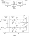
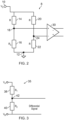
- the sensor 2 may be based on many types of circuit configuration, common examples of which include Wheatstone Bridges (as shown in Figure 2 ) and potential dividers (as shown in Figure 3 ).
- the sensor 2 has several arrows pointing into it. These represent inputs that affect the output of the sensor. Inputs include electrical signals to energize the sensor, and the common mode output voltage and differential response of the sensor may vary as a function of the input signals (which may be one or more voltages or currents) that energize it.
- Some sensors only measure a parameter of one of the input voltages supplied to it whereas other sensors may output one or more signals as a function of two (or more) input voltages or currents.
- Other sensors may measure physical parameters such as pressure, strain, fluid flow rates or strength and direction of magnetic fields. Consequently the inputs to the sensor 2 are potentially both electrical and wanted physical parameters. Unwanted physical parameters, such as changes in temperature may also affect the sensor or supply voltage fluctuations which might also affect the sensor.
- the sensor 2 outputs differential signals to the differential signal processing system 4.
- the Wheatstone Bridge 8 is connected between two voltage supply nodes 10 and 12.
- node 10 is supplied with a voltage Vs and node 12 is a ground node.
- First and second impedances 14 and 16 are connected in series between nodes 10 and 12, and define a first intermediate node 18.
- a second set of series connected impedances 20 and 22 are connected between nodes 10 and 12 and define second intermediate node 24.
- the nodes 18 and 24 represent outputs of the Wheatstone bridge 8 which are connected to a differential amplifier 30.
- the Wheatstone bridge can be driven with DC or AC voltages. Suppose the bridge 8 is driven with a DC voltage Vs and all of the impedances are resistive with a value R.
- the Wheatstone bridge can include components other than resistors, such as capacitors, inductors and semiconducting components.
- Figure 3 shows a potential divider 35, which really is half of a Wheatstone bridge. It comprises two impedances, in this case resistors 38 and 40 of value R1 and R2 connected in series between nodes at voltages V A and V B . The difference V A -V B is divided by the ratio R2/(R1+R2). A differential output signal is developed across R2. If either V A or V B varies, then the common mode value of the differential signal also varies.
- a potential divider is used to measure voltage difference between the voltage V A at one end of the potential divider compared to the voltage V B at the other end of the potential divider in circumstances where the voltage difference may be, or is known to be, beyond the operating range of the subsequent signal processing circuits.
- Divide ratios may be quite large such that voltages occurring in electricity distribution systems can be converted to voltages in the order of a few hundreds of millivolts. This requires the transfer ratio of the voltage divider and the subsequent signal processing circuits to be known to a desired accuracy. Often the accuracy is mandated by a customer or by a standards body. Accuracies of 0.1% are commonly mandated.
- FIG. 4 schematically illustrates an example of an amplifier that may be used to process the signals from the sensor circuit 2.
- the amplifier 30 is implemented as a switched capacitor device, as this technology sits well with systems where a switched capacitor Analog to Digital converter (ADC) is used to digitize the input signal.
- ADC Analog to Digital converter
- the amplifier 30 is connected to an antialiasing filter 50 in order to attenuate signals above a filter cut off frequency such that there is little significant energy in signal components approaching half of the switching frequency of the amplifier 30.
- the amplifier being a differential device, has two input sampling arrangements 60a and 60b, each comprising a sampling capacitor 62a and 62b in association with a respective switch network such that the capacitor 62a can connected to the input node 52 by way of the filter 50 during a sample phase to acquire the input voltage of node 52.
- the capacitor 62a can then be placed in a hold phase where it is disconnected from the input node 52 and from an associated node 64a of an operational amplifier 70.
- the capacitor may then be connected to the node 64a such that it undergoes charge exchange with a feedback capacitor 72a of the amplifier 70.
- the capacitor 62a may optionally be reset by connecting both its plates together, or to a voltage such as ground.
- the feedback capacitor may also be reset during this phase by an associated shorting switch 74a.
- Similar components exist for the other input channel (and are designated by a "b" suffix in Figure 4 ) and are operated in the same way.
- V t Vs 1 ⁇ e ⁇ t RC
- the voltage V(t) rises towards the "correct" value Vs in an exponential manner.
- the upshot of this response it that if one wishes to measure a signal and the signal is acquired by a sampling circuit having an RC time constant, one must wait at least seven times the time constant for V(t) to rise to within 0.1% of Vs. Waiting eight times the RC time constant delivers 0.04% accuracy. If a fixed amount of waiting time is budgeted for the sample part of the sample and hold process, then a change in the time constant changes the amount by which V(t) has approached Vs. This is only one example of a way in which changes in the common mode voltage can affect the operation of the differential signal processing circuit. Additionally the impedance of the transistor switches can also interact with the components of the anti-aliasing filter.
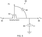
- the circuit comprises a Field effect transistor 82, which in this example is an NMOS device, having its source connected to an input node 84 at which an input voltage Vin exists.
- a drain of the transistor 82 is connected to an output node 86 and to a sampling capacitor 88 having a value C hold .
- the switching operation of the circuit is primarily controlled by a clock signal Phi. When Phi is high, transistor 82 is conducting and the voltage Vin at the input node 84 causes charge to be stored on the capacitor C hold .
- the transistor 82 When Phi goes low, the transistor 82 becomes high resistance, and the charge is held stored on the capacitor 88. However this simple operation requires further analysis. In use the transistor 82 exhibits an on resistance, Rds-on. When a MOSFET is driven as a switch the gate voltage is usually driven to either supply rail so as to switch the device hard on or hard off. If the input voltage approaches the positive rail voltage Vdd, then the difference between Phi (when asserted) and Vin may not be sufficient to switch the transistor on properly. This gives rise to a change in the ON resistance Rds-on which varies as a function of the input voltage.
- V T V FB + ⁇ 2 ⁇ f + V SB ⁇ 2 ⁇ f
- Vt includes a term V SB which represents the voltage difference between the source of the FET and the body material of the device, which is generally connected to a "back gate" node.
- V T ⁇ 2 ⁇ f + V SB ⁇ 2 ⁇ f
- the on resistance varies in relation to the input voltage Vin. It can also be seen that the transistor 82 and the capacitor 88 form a low pass filter during the sample or track mode. The time constant of the filter depends on the input voltage and this is undesirable.
- parasitic capacitances represented in Figure 5 by capacitor 90, can also cause charge to be exchanged with the sampling capacitor when the drive signal Phi changes state.
- the size of the charge on the parasitic capacitance is also be modulated by the voltage difference between the source and gate of the transistor 82. There is a similar parasitic capacitance between the gate and the input (drain) of the switch.
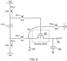
- the bootstrap circuit includes additional transistor switches Sw1 to Sw5, and a bootstrap capacitor 112. Starting with phi-1 not asserted and Phi-2 asserted prior to switching the sampling switch 82 to conduct, the switches sw3 and sw4 are initially closed to charge the bootstrap capacitor 112 to Vdd. Then the clock signal Phi1 is asserted and phi2 un-asserted in a non-overlapping manner. Switches Sw1 and Sw2 close and all the other switches open. The lower plate of the bootstrap capacitor assumes the input voltage Vin. As a consequence, the gate voltage is always Vin +Vdd because of the voltage difference across the floating bootstrap capacitor.
- FIG. 7 schematically illustrates a signal processing circuit comprising a differential Analog to Digital converter (ADC) in a circuit constituting an embodiment of the present disclosure.
- the differential analog to digital converter 150 can be a standard component implemented using any suitable technology.
- the ADC 150 may be in the form of a sigma-delta converter with a switched capacitor input stage or a switched capacitor successive approximation converter such that it serves as its own sample and hold device.
- the ADC 150 receives first and second input voltages V1 and V2 at its first and second inputs 152 and 154 respectively from an input circuit 2 as previously discussed.
- the first and second voltages V1 and V2 can be represented by a common mode component Vcm and a differential component Vdiff.
- the voltage source 162 generates a voltage V162 with a magnitude half the differential voltage Vdiff.
- the voltage source 164 generates a voltage V164 with the same magnitude but with opposite polarity to the voltage source 162.
- V 162 V 164
- Vcm V1 and/or V2
- the sensor 2 may be actively arranged to receive a time varying stimulus Vstim from stimulus generator 170.
- the stimulus is a voltage varying between 0 and Vstim. Therefore in the arrangement shown in Figure 7 the common mode value of V1 and V2 varies in time varying manner between Vcm and Vcm + Vstim.
- the changes may be proportional to the change in common mode voltage.
- the suitable amount may be learnt or estimated based on knowledge of the characteristics of the input circuit 2 and knowledge of the size of the stimulus voltage Vstim.
- the modulation of the supply rails or the control signals can include effectively shifting (voltage translating) the signals and/or scaling them.
- the circuit shown in Figure 7 includes two voltage regulators 182 and 184 which have a variable output voltage and which are responsive to control signals provided by a voltage correction signal generator 180.
- the first voltage regulator 182 is provided between the most positive supply rail Vdd and the positive supply input Vdd' of the analog to digital converter 150.
- the first voltage regulator 182 converts the nominally fixed Vdd voltage to a variable voltage Vdd' which is provided to the +ve supply input analog to digital converter 150.
- the second voltage regulator 184 is connected between the negative supply pin Vss' of the analog to digital converter 150 and the most negative (or least positive) supply rail Vss such that Vss' is variable under the control of the voltage correction signal generator 180.
- the nature of the stimulus could vary widely, it could be piece wise linear form, for example a square wave with or without slew rate limited transitions, a sine wave or something more complicated.
- the regulators 182 and 184 may be implemented as linear circuits such as low drop out voltage regulators, for example as source followers possibly stabilized within a feedback loop of an operational amplifier.
- switched mode regulators may be used, depending on choices such as power efficiency, power consumption and tolerance of noise from the switched mode supply.
- the correction signal generator 180 receives an indication of the status of the stimulus generator 170, either by monitoring the output of the voltage stimulus generator 170 or by being provided with a logic signal representing the status of the stimulus generator 170.
- a control signal for the stimulus generator 170 is provided to the correction signal generator 180 for generation of a correction signal.
- the magnitude of the correction is generated in an open loop manner, i.e. from assumptions or prior knowledge about the signal output from the stimulus generator 170.
- the control inputs to the stimulus generator 170 and to the correction signal generator 180 do not need to be identical.
- the signals might have different assertion times, different length and/or in the case of multibit signals differing bit depths as long as objective of making the signal from the correction signal generator appropriate for the purpose of reducing the amount of unwanted differential signal change resulting from prevailing the common mode value of the stimulus.
- the correction signal generator 180 monitors the output of the stimulus generator 170 and may use this signal to generate a correction signal. This approach has the potential to more accurately account for use of inexpensive stimulus generators which may have, for example, limited slew rates.
- Figure 10 schematically shows a modification to the arrangement shown in Figure 7 .
- An output signal from the correction signal generator 180 is provided to the differential signal processing circuit 4, which is this example comprises ADC 150.
- the correction signal is provided to circuits 182, 200 and 202 to correct the supply voltage Vdd, a reference voltage and the clock voltage, respectively.
- the ground voltage may also be modified.
- Figure 11 shows how the correction signal from the correction signal generator may be used with a signal processing circuit 4 comprising a differential amplifier 210, here shown as a device having a dual ended output.
- a differential amplifier 210 may be known as a difference amplifier.
- the amplifier 210 may not be a switched capacitor device so only the power supply rail voltages need to be modified by the circuit 182, and indeed such modification need only be applied to the input stage of the amplifier 210. If the amplifier was a switched capacitor device then the clock signals used to control the transistor switches may also be level shifted or modified.
- the power requirements of the transistors implementing the sampling switches within a differential amplifier configuration (which may be part of the analog to digital converter 150) are generally very modest. The inventors realized that in some cases this can be a very efficient way to implement the invention.
- Figure 12 shows a further embodiment of this disclosure, where a Voltage Vin at node 290 is being measured, for example as part of a metrology device such as a power consumption meter.
- Vin may be at several hundred volts RMS so may easily have a peak value in the 300V range.
- the input voltage may be input to a resistive potential divider comprised of resistors 300 and 302.
- the resistors 300 and 302 have been set to make a potential divider with a nominal divide ratio of 1000 times. If the meter requires 0.2% accuracy then the resistor ratios have to be correct to within a ratio of 1 to 500000 times.
- Analog Devices Inc. has several proposals which simplify the constraints on the resistor accuracy by applying a known reference signal to the potential divider, and using the reference signal to characterize the transfer function of the potential divider and its signal processing chain.
- the reference signal can be supplied by a stimulus generator 170, and supplied to a node of the resistor 302 by way of a suitable buffer, such as an operational amplifier 306.
- a suitable buffer such as an operational amplifier 306.
- the processing steps used to characterize the response of the potential divider (and indeed other sensors) and the signal processing chain are described in WO2014191776 , WO2014072733 , US9151818 , WO2013038176 , and US9322850 . Briefly a known reference signal is passed through the measurement circuit. As will be shown, the measurement circuit has an effect on the reference signal, and a careful comparison of the effected reference signal with the original reference signal allows the transfer characteristic of the measurement signal to be estimated.
- the divider has divide ratio of 1000 times, that Vin is 300V and that the reference signal at the output of the amplifier 306 varies between 0 V and 400mV with respect to ground.
- the reference signal is at 0V
- the reference signal is 400mV
- the acquisition and processing circuit 4 is a differential circuit which has a sampling input in each channel, with one of the differential inputs being connected to node 310 and the other input being connected to node 312.
- this comprises a first transistor switch 350a connected between node 310 and a first plate 360a of a sampling capacitor 362a.
- a second plate of the capacitor 362a is connected to a small signal ground.
- the first plate 360a is connected by way of a second transistor switch 370a to an input of a differential amplifier 210 which in this example is provided with feedback capacitors 380a and 380b such that it implements amplification by way of charge sharing between the sampling capacitors and the feedback capacitors.
- Shorting switches associated with the capacitors or circuits for adjusting the common mode output voltage have been omitted for simplicity but are known to the person skilled in the art.
- the anti-aliasing filter has been omitted for the purpose of simplifying the explanation, but may be assumed to be present.
- the switches 350a and 370a are driven in antiphase by respective non-overlapping clock signals.
- the requisite drive signals can be derived from a single clock signal CLK by way of suitable circuits represented here by a non-inverting buffer 400 receiving the signal CLK and driving the first switch 350a (and a corresponding switch 350b in the other input path) and an inverting buffer 402 receiving the clock signal CLK and driving the second switches 370a and 370b.
- the switches are active when driven high, as would be the case with NMOS devices, but the person skilled in the art could use PMOS switches or a transmission gate architecture using parallel NMOS and PMOS devices each having a respective drive signal.
- Each of the drivers, namely buffer 400 and inverter 402 is connected to the supply nodes Vdd' and Vss' as described with respect to Figure 7 (the outputs of the voltage modification circuits 182 and 184, respectively).
- the voltages applied to drive the switches can be varied by the correction voltage generator 180 in response to changes in the common mode voltage.
- the correction signal may be supplied to the back gate node of the transistors (the back gate being an intrinsic feature of a FET) such that the device threshold can be varied as a function of the gate voltage or the common mode voltage so as to manipulate the on state resistance of the FET acting as a switch.
- the approach of adjusting the clock signal voltage to follow changes in the common mode voltage resulting from the application of the stimulus signal may be applied to other switching circuits, such as chopping (cross-over) circuits used to route the differential signal in a straight through path or a swapped path to an amplifier for the purpose of removing input offsets within the amplifier.
- chopping cross-over
- a first input node 400 can be selectively connected to either a first output node 402 or to a second output node 402 by way of transistor switches 406 and 408, respectively.
- a second input node 410 can be connected to the output nodes 404 and 402 by transistor switches 416 and 418, respectively.
- the switches 406 and 416 are driven by a first clock voltage represented by voltage source 420.
- the switches 408 and 418 are driven by a second clock represented by voltage source 422. Both the voltage sources are referenced with respect to a correction signal output by the correction signal generator 180.
- the clock signals are non-overlapping (implementing a break before make switching function) and the second clock is inverted with respect to the first clock.
- Figure 14 schematically illustrates an embodiment of a circuit for modifying the digital drive signal voltage applied to a switching transistor as a function of a stimulus voltage of known size applied to a measurement circuit 2.
- a transistor acting as a sampling switch 440 is connected between an input node 442 and a sampling capacitor 450.
- Other components connected to the sampling capacitor 450 have been omitted for clarity.
- a gate of the switching transistor 440 receives a control signal from a suitable logic driver 460, such as an inverter 460.
- the inverter may be responsive to a clock signal (which in this example causes a sample to be taken when the clock is low and a hold to be performed when the clock is high).
- a resistor 470 having a resistance R LS is connected between the output of the inverter 460 and the gate of the sampling transistor 440.
- the gate of the sampling transistor is also connected to a current source that sources (or sinks) a current Iref.
- the current Iref is switchable, in this example by the inclusion of a switch LS1 between the current source 480 and the gate of the sampling transistor 440.
- the person skilled in the art could use alternative approaches, such as inhibiting the drive to a transistor forming the current source itself or using additional current steering switches.
- the voltage shift applied to the gate by actuation of the switch LS1 can be set to match the change in common mode voltage at the input node 442 resulting from the application of the excitation signal by the excitation signal generator 170.
- the back gate of the sampling transistor 440 can be driven by a second level shifting circuit comprising a second resistor 470a having value R LS and a second current source 480a selectively supplying a current Iref, for example by way of a second level shifting switch LS2 such that the back gate voltage can be set to 0V or to Iref*R LS volts depending on the status of switch LS2.
- the switches LS1 and LS2 are driven from the control signal used to instruct the excitation signal to switch to an on state.
- the fixed current sources/sinks 480 and 480a may be replaced by variable current sources. This can be done, as shown in Figure 15 , in a digital domain by replacing the current sources 480 and 480a and optionally their associated switches by current digital to analog converters 490 and 490a, respectively, which are driven by multibit control words.
- the words may be derived from the correction signal generator.
- the correction signal generator may include its own ADC so as to estimate the near instantaneous value of the excitation signal or of the common mode voltage change resulting from application of the excitation signal.
- FIG 16 shows a circuit where the current sources 480 and 480a are replaced with slave stages of a current mirror 500 and the excitation voltage is monitored and used to set the current flowing in the current mirror 500.
- the excitation voltage from the stimulus generator 170 ( figures 7 to 9 ) is supplied to the non-inverting input of an operational amplifier 510 having its output connected to the gate of an n type FET 520.
- a source of the FET 520 is connected to a load resistor 530 which is connected to ground. The voltage across the resistor is sensed at the inverting input of the amplifier 510.
- the feedback loop around the amplifier causes the voltage across the resistor to match the voltage at the non-inverting input of the amplifier 510, i.e. the excitation voltage in this example.
- This voltage is converted into a current by the resistor 530 and the current flowing in the resistor 530 is mirrored by the current mirror to the resistors 470 and 470a.
- a possible implementation of the current mirror is shown in Figure 17 based on p-type MOSFETS with a master transistor 550 being diode connected and connected to the source of the transistor 520 of figure 16 , and slave transistors 552 and 554 are connected to the gate of the master transistor, as known to the person skilled in the art.
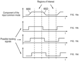
- Figure 18a illustrates that the common mode voltage may transition over periods 600 and 602 and that the transitions need not be instantaneous. This may be the result of not seeking to output a square wave from the excitation generator, for example to avoid the harmonic components associated with square waves or because it is cheaper and/or easier to allow the transition to be RC or slew rate limited.
- the common mode offset correction need not be correct all of the time. It only needs to be achieved during regions of interest, for example when the sample switches of the processing circuits are closed (sampling the input signal). The timing of the correction signals supplied to the gate and back gate of the sampling transistors can be quite flexible.
- Figures 18b, 18c and 18d all show possible valid correction signals.
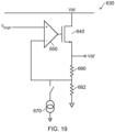
- FIG 19 shows an implementation of a linear voltage regulator 630 that may be used to control Vdd'.
- the regulator comprises an N type FET, here MOSFET 640 with its drain connected to the supply rail Vdd and its source outputting the modified voltage Vdd'.
- the MOSFET 640 is included within the feedback loop of operational amplifier 630 which has its inverting input connected to the source of MOSFET 640 by way of a potential divider comprising resistors 660 and 662, and its non-inverting input receiving the target voltage "Vtarget" which matches the desired Vdd' as divided down by the potential divider.
- Vtarget target voltage
- a current may be sunk by a current source 670 causing an additional voltage drop to occur across the resistor 660, which causes the feedback loop to increase Vdd'.
- the current source 670 may be replaced by a current DAC
- a similar circuit can be used to control Vss' but would naturally involve a P type FET.
- Figure 20 shows a circuit arrangement like that described with respect to Figure 16 connected to a potential divider and a stimulus generator 170 as was described with respect to Figure 12 .
- the drive signal correction for adjusting the voltage of the digital drive signal CLK to track with the changes in the common mode voltage of the differential signal can be achieved by connecting the non-inverting input of the operational amplifier 510 to receive the stimulation signal from the stimulus generator 170. This is achieved in this example by connecting the amplifier to node 312.
- the voltage differences developed by the currents from the current mirror 500 flowing through the resistors 470 and 470a are provided to the gates and back gates, respectively, of transistors 440a and 440b acting as sampling switches within the differential signal processing circuit 4. Only the very front end of the differential signal processing circuit is illustrated.
- the differential inputs of the differential signal processing circuit 4 are connected to nodes 310 and 312 either side of resistor 302.
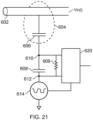
- FIG 21 schematically shows an arrangement in which a conductor 602 has the time varying voltage V in (t) which we desire to measure.
- the voltage V in (t) may be exceptionally high, and therefore galvanic connection to the conductor may be highly undesirable.
- non-contacting or galvanically isolated approaches can be adopted.
- a mechanical clamp, a hook, an open jaw or similar structure can be provided to facilitate removable introduction of a voltage probe to a conductor.
- more permanent structures such as rings or plates can be placed or otherwise fixed around or in close proximity to the conductor.
- the conductor has an insulation layer, but the clamp, hook, jaw, ring or so on may be associated with an insulator such that it can be used with non-insulated conductors or other arrangements, such as spacing arrangements, can be used to hold a plate or electrode of the sensing arrangement adjacent but spaced from the conductor.
- the clamp, hook, jaw, ring or so on forms a capacitor coupled with the conductor 602.
- the probe is designated by the chain line 604 and the capacitor formed by the interaction between the conductors of the probe 604 and the voltage carrying conductor 602 is designated 606.
- the capacitor 606 is of an unknown value.
- the unknown capacitor 606 is formed in series with a measurement capacitor 608.
- a first node 610 is formed between the unknown capacitor 606 and the measurement capacitor 608 and is connected to a first input of a measurement circuit 620.
- a second node 612 is formed between a second plate of the measurement capacitor 608 and a reference voltage generator 614.
- the node 612 is connected to a further input of the measurement circuit 620.
- the measurement circuit is also connected to the voltage generator 614 for example to control the operation of the voltage generator 614.
- the first node 610 is generally associated with some means of controlling or restoring a DC voltage across the second capacitor 608.
- Various approaches could be adopted.
- a resistor 609 may be placed in parallel with capacitor 608 to provide a DC discharge path.
- a high impedance path to a bias voltage may be provided to place a known DC voltage at node 610 and hence on the capacitor 608.
- This approach can help simplify the design of the input stage of the measurement circuit by enabling the voltage at node 610 to be set to a value that simplifies the biasing of an input transistor of the input stage.
- the voltage generator 614 can provide a DC component to node 612 to simplify the design of the input stage.
- the voltage generator 614 is used to create a relatively small perturbation to the voltage at node 612. Furthermore this perturbation is generally at a frequency different to the frequency of the input signal V in (t).
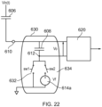
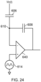
- Figure 22 shows an embodiment of an arrangement of Figure 21 in greater detail.
- the measurement capacitor 608 and the voltage generator 614 are illustrated as being within an input circuit 630.
- the signal generator is formed as a combination of a first switch 632 extending between the second node 612 and ground, and a second switch 634 which extends between the second node 612 and a DC voltage reference 614a providing a fixed output voltage Vf.
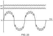
- the switches 632 and 634 are energized by signals sw1 and sw2 from the switch controller (not shown).
- Figure 23 shows the switch control signals sw1 and sw2 and the fact that they are driven in antiphase. Figure 23 also shows how operation of the switches effects the output voltage Vo developed between nodes 610 and 612.
- the capacitors 606 and 608 form a capacitive divider and consequently, if the conductor 602 is carrying a mains electricity signal, then the output voltage Vo corresponds to a divided down version of that mains signal.
- the divide ratio depends on the relative sizes of the known capacitor 608 and the unknown capacitor 606.
- the unknown capacitor 606 and the feedback capacitor 608 can be arranged around an operational amplifier 640 in a virtual earth configuration. Again steps can be taken to restore node 610 to a desired DC value, for example by placing resistor 609 (not shown) in parallel with capacitor 608. This approach facilitates DC restoration and also provides protection against leakage currents being integrated onto capacitor 608 and eventually driving the amplifier 640 into saturation.
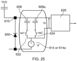
- FIG 25 illustrates a further embodiment where the capacitance of the measurement capacitor 608 can be varied, for example by using the switches 632 and 634 to switch between two measurement capacitors or to bring a further capacitor in parallel with the measurement capacitor.
- a further capacitor 608a is provided in parallel with the measurement capacitor 608 such that they can be swapped in and out of the potential divider.
- the switches 632 and 634 may connect directly to ground or they may connect via a voltage source 614 or 614a.
- a voltage offset may make the design of the input stage of the data processing apparatus 620 easier.
- a modulated voltage could also be provided thereby allowing additional degrees of freedom in seeking to characterize the transfer function of the potential divider formed between the capacitors 608 and the unknown capacitor 606.
- a protection arrangement such as a voltage clamping diode 650 may be provided between node 610 and ground in order to protect the electronics of the measurement circuit.
- the data processor may output a digital code directly representative of the voltage V in (t) or might simply provide an indication of the transfer function of the potential divider network.
- a non-contacting voltage measurement apparatus in which the reference signal generator generates a signal of amplitude less than 30 V peak to peak.
- a non-contacting voltage measurement apparatus in which the reference signal generator generates a reference signal of less than 10 V peak to peak.
- a non-contacting voltage measurement apparatus further comprising a signal processing apparatus for receiving the voltage across the measurement capacitor and the reference signal, and estimating a transfer function of the potential divider and/or the voltage of the conductor.
- a non-contacting voltage measurement apparatus in which the signal processing apparatus is based on the teachings of WO2014/072733 or WO2013/038176 where a small perturbing signal is used with a divider network to characterize the transfer function of the divider network.
- the inputs may originate from a variety of transducers, such as a current shunt such that the voltage across the shunt is representative of the current in the shunt, as might be found in a RF amplifier gain control circuit.
- the differential signal processing circuit may be used in industrial control, instrumentation or power metering applications. Alternatively the voltage may derive from a component in an attenuator circuit.
Landscapes
- Engineering & Computer Science (AREA)
- Physics & Mathematics (AREA)
- General Physics & Mathematics (AREA)
- Theoretical Computer Science (AREA)
- Power Engineering (AREA)
- Computer Networks & Wireless Communication (AREA)
- Signal Processing (AREA)
- Amplifiers (AREA)
- Measurement Of Current Or Voltage (AREA)
Claims (14)
- Vorrichtung, die Folgendes umfasst:eine aktive Schaltung, wobei die aktive Schaltung (180, 182, 184) konfiguriert ist, eine Steuerspannung mindestens eines Transistorschalters (350a) einer Differenzverarbeitungsschaltung (4, 210) zum Verbessern der Gleichtaktunterdrückung der Differenzverarbeitungsschaltung einzustellen,wobei die Vorrichtung ferner Folgendes umfasst:eine Messschaltung (2; 300, 302), die konfiguriert ist, ein erstes und ein zweites Signal, die zusammen ein Differenzsignal bilden, für die Differenzsignalverarbeitungsschaltung bereitzustellen, wobei die Differenzsignalverarbeitungsschaltung einen ersten Kanal und einen zweiten Kanal zum Empfangen des ersten bzw. des zweiten Signals aufweist und jeder des ersten Kanals und des zweiten Kanals eine jeweilige Abtast-/Halteschaltung umfasst, die an den entsprechenden Eingang eines Differenzsignalverstärkers der Differenzsignalverarbeitungsschaltung gekoppelt ist,wobei die Messschaltung (300, 302) einen ersten (290) und einen zweiten (312) Eingangsknoten und einen Ausgangsknoten (310) umfasst, der erste Eingangsknoten (290) ausgelegt ist, ein zu messendes Eingangssignal zu empfangen, die Messschaltung konfiguriert ist, das Eingangssignal auf der Grundlage einer Übertragungscharakteristik der Messschaltung zu verarbeiten und ein Ausgangssignal bei dem Ausgangsknoten bereitzustellen, und der zweite Eingangsknoten (312) ausgelegt ist, ein bekanntes Stimulationssignal zum Charakterisieren einer Übertragungscharakteristik der Messschaltung zu empfangen,der erste Kanal der Differenzsignalverarbeitungsschaltung mit dem Ausgangsknoten der Messschaltung verbunden ist und der zweite Kanal der Differenzsignalverarbeitungsschaltung mit dem zweiten Eingangsknoten der Messschaltung oder mit einem zweiten Ausgang der Messschaltung verbunden ist,das erste Signal durch den mindestens einen Transistorschalter (350a) geschaltet wird, wobei der mindestens eine Transistorschalter konfiguriert ist, als ein Abtastschalter in der Abtast-/Halteschaltung des ersten Kanals der Differenzsignalverarbeitungsschaltung zu arbeiten,die Gleichtaktspannung des Differenzsignals, das durch die Messschaltung bereitgestellt wird, eine Funktion des bekannten Stimulationssignals ist, wobei das bekannte Stimulationssignal von der Gleichtaktspannung verschieden ist, unddas Einstellen der Steuerspannung eine Funktion des bekannten Stimulationssignals ist.
- Vorrichtung nach Anspruch 1, wobei die Vorrichtung ferner ausgelegt ist, die Steuerspannung durch Abwandeln eines Ansteuersignals, das den mindestens einen Transistorschalter durch Anwenden einer Modulation oder einer Spannungsübersetzung auf das Ansteuersignal ansteuert, auf der Grundlage des bekannten Stimulationssignals derart einzustellen, dass die eingestellte Steuerspannung die Spannung des geänderten Ansteuersignals ist.
- Vorrichtung nach einem vorhergehenden Anspruch, wobei die Vorrichtung ausgelegt ist zum:Überwachen einer Ausgabe einer Erregungsschaltung (170), die ausgelegt ist, das bekannte Stimulationssignal anzulegen; undVariieren der Gate-Spannung des mindestens einen Transistorschalters (350a) in Reaktion auf die Ausgabe.
- Vorrichtung nach einem vorhergehenden Anspruch, wobei die Vorrichtung ausgelegt ist zum:Überwachen eines Steuersignals, das einer Erregungsschaltung (170) zugeführt wird, die ausgelegt ist, das bekannte Stimulationssignal anzulegen; undVariieren der Gate-Spannung des mindestens einen Transistorschalters (350a) in Reaktion auf das Steuersignal.
- Vorrichtung nach einem vorhergehenden Anspruch, wobei die Vorrichtung konfiguriert ist, die Gate-Spannung des mindestens einen Transistors (350a) als eine Funktion der Gleichtaktspannung des Differenzsignals, das aus dem Anlegen des bekannten Stimulationssignals resultiert, zu variieren und die Vorrichtung ferner wahlweise konfiguriert ist, die Gate-Spannung des mindestens einen Transistorschalters (350a) als eine Funktion der Änderung der Gleichtaktspannung des Differenzsignals, die aus einer Änderung des bekannten Stimulationssignals resultiert, zu variieren.
- Vorrichtung nach einem vorhergehenden Anspruch, wobei die aktive Schaltung (180) konfiguriert ist, eine Magnitude oder einen Zeitablauf des bekannten Stimulationssignals zu empfangen.
- Vorrichtung nach einem vorhergehenden Anspruch, wobei der mindestens eine Transistor, der konfiguriert ist, als ein Abtastschalter zu arbeiten, Teil eines Verstärkers, eines Integrators oder eines Analog/Digital-Umsetzers ist.
- Vorrichtung nach Anspruch 6 oder Anspruch 7, die ferner einen Stimulusgenerator (170) umfasst, um das Stimulationssignal zu erzeugen, das an die Messschaltung, die mit der Signalverarbeitungsschaltung (4; 210) verbunden ist, derart angelegt wird, dass die Differenz- und die Gleichtaktspannung an den Eingängen (310, 312) der Signalverarbeitungsschaltung durch das Stimulationssignal geändert werden; und
wobei die Messschaltung (2) wahlweise ein Potentialteiler (300, 302) ist, der einen ersten (290) und einen zweiten Eingangsknoten (312) und einen Ausgangsknoten (310) aufweist, der erste Eingangsknoten (290) ausgelegt ist, eine Spannung zu empfangen, die gedämpft und verarbeitet werden soll, der zweite Eingangsknoten (312) ausgelegt ist, das Stimulationssignal zu empfangen, und der erste Eingang der Differenzsignalverarbeitungsschaltung mit dem Ausgangsknoten des Potentialteilers verbunden ist und der zweiten Eingang der Differenzsignalverarbeitungsschaltung mit dem zweiten Eingangsknoten des Potentialteilers oder mit einem zweiten Ausgang des Potentialteilers verbunden ist. - Vorrichtung nach Anspruch 8, die ferner einen Korrektursignalgenerator (180) umfasst, der auf den Stimulusgenerator (170) anspricht, um ein Korrektursignal zum Steuern der Änderung der Steuerspannung zu erzeugen.
- Vorrichtung nach einem der Ansprüche 7-9, wobei die Differenzsignalverarbeitungsschaltung einen Analog/Digital-Umsetzer mit geschaltetem Kondensator umfasst und die aktive Schaltung ausgelegt ist, die erste und die zweite Versorgungsspannung des Analog/Digital-Umsetzers als eine Funktion der Gleichtaktspannung des Differenzsignals zu modifizieren.
- Vorrichtung nach einem der Ansprüche 1-10, wobei ein Steueranschluss des mindestens einen Transistors (350a) an mindestens eine Versorgungsspannung (Vdd, Vss) der Differenzsignalverarbeitungsschaltung gekoppelt ist und das Einstellen der Steuerspannung des mindestens einen Transistors (350a) ein Einstellen der mindestens einen Versorgungsspannung (Vdd, Vss) der Differenzsignalverarbeitungsschaltung umfasst.
- Verfahren zum Verbessern der Gleichtaktunterdrückung einer Differenzschaltung unter Verwendung der Vorrichtung nach einem der Ansprüche 1-11, wobei das Verfahren Folgendes umfasst:Bereitstellen unter Verwendung der Messschaltung des ersten und des zweiten Signals, die zusammen ein Differenzsignal bilden, für die Differenzsignalverarbeitungsschaltung;Empfangen des bekannten Stimulationssignals durch die Messschaltung zum Charakterisieren einer Übertragungscharakteristik der Messschaltung undEinstellen der Steuerspannung des mindestens einen Transistorschalters der Differenzsignalverarbeitungsschaltung,wobei das erste Signal durch den mindestens einen Transistorschalter geschaltet wird,die Gleichtaktspannung des Differenzsignals, das durch die Messschaltung bereitgestellt wird, eine Funktion des bekannten Stimulationssignals ist, das an die Messschaltung angelegt wird, wobei das bekannte Stimulationssignal von der Gleichtaktspannung verschieden ist, unddas Einstellen der Steuerspannung eine Funktion des bekannten Stimulationssignals ist, das an die Messschaltung angelegt wird.
- Verfahren zum Verbessern der Gleichtaktunterdrückung einer Differenzschaltung nach Anspruch 12, wobei das Einstellen der Steuerspannung des mindestens einen Transistorschalters Folgendes umfasst:(i) Variieren einer ersten und einer zweiten Versorgungsspannung der Differenzschaltung als eine Funktion des Gleichtaktwerts eines Differenzeingangssignals, wobei ein Steueranschluss des mindestens einen Transistorschalters konfiguriert ist, an mindestens eine der ersten und der zweiten Versorgungsspannung der Differenzschaltung gekoppelt zu sein;(ii) Variieren eines nominellen digitalen Steuersignals, das an ein Gate des mindestens einen Transistors angelegt wird, als eine Funktion der Gleichtaktspannung des Differenzsignals, wobei der mindestens eine Transistor ein Feldeffekttransistor (350a) ist, und(iii) Variieren einer Back-Gate-Spannung des mindestens einen Transistors als eine Funktion des Gleichtaktwerts des Differenzeingangssignals, wobei der mindestens eine Transistor ein Feldeffekttransistor (350a) ist.
- Verfahren nach Anspruch 12 oder 13, wobei das Einstellen der Steuerspannung ein Messen einer Änderung der Gleichtaktspannung als Grundlage verwendet.
Priority Applications (1)
| Application Number | Priority Date | Filing Date | Title |
|---|---|---|---|
| EP24196620.9A EP4446754A3 (de) | 2017-09-08 | 2018-09-06 | Verfahren und vorrichtung zur verringerung des einflusses eines gleichtaktsignals auf ein differenzsignal und systeme mit solch einer vorrichtung |
Applications Claiming Priority (4)
| Application Number | Priority Date | Filing Date | Title |
|---|---|---|---|
| US201762555979P | 2017-09-08 | 2017-09-08 | |
| GBGB1801910.9A GB201801910D0 (en) | 2018-02-06 | 2018-02-06 | A non-contacting voltage measuring apparatus |
| US16/015,657 US10892722B2 (en) | 2017-09-08 | 2018-06-22 | Method of and apparatus for reducing the influence of a common mode signal on a differential signal and to systems including such an apparatus |
| PCT/EP2018/074071 WO2019048579A1 (en) | 2017-09-08 | 2018-09-06 | METHOD AND APPARATUS FOR REDUCING THE INFLUENCE OF A COMMON MODE SIGNAL ON A DIFFERENTIAL SIGNAL AND SYSTEMS COMPRISING SAID APPARATUS |
Related Child Applications (2)
| Application Number | Title | Priority Date | Filing Date |
|---|---|---|---|
| EP24196620.9A Division EP4446754A3 (de) | 2017-09-08 | 2018-09-06 | Verfahren und vorrichtung zur verringerung des einflusses eines gleichtaktsignals auf ein differenzsignal und systeme mit solch einer vorrichtung |
| EP24196620.9A Division-Into EP4446754A3 (de) | 2017-09-08 | 2018-09-06 | Verfahren und vorrichtung zur verringerung des einflusses eines gleichtaktsignals auf ein differenzsignal und systeme mit solch einer vorrichtung |
Publications (2)
| Publication Number | Publication Date |
|---|---|
| EP3679653A1 EP3679653A1 (de) | 2020-07-15 |
| EP3679653B1 true EP3679653B1 (de) | 2024-10-30 |
Family
ID=61730819
Family Applications (2)
| Application Number | Title | Priority Date | Filing Date |
|---|---|---|---|
| EP24196620.9A Pending EP4446754A3 (de) | 2017-09-08 | 2018-09-06 | Verfahren und vorrichtung zur verringerung des einflusses eines gleichtaktsignals auf ein differenzsignal und systeme mit solch einer vorrichtung |
| EP18786679.3A Active EP3679653B1 (de) | 2017-09-08 | 2018-09-06 | Verfahren und vorrichtung zur reduzierung des einflusses eines gleichtaktsignals auf ein differenzsignal und auf systeme mit einer solchen vorrichtung |
Family Applications Before (1)
| Application Number | Title | Priority Date | Filing Date |
|---|---|---|---|
| EP24196620.9A Pending EP4446754A3 (de) | 2017-09-08 | 2018-09-06 | Verfahren und vorrichtung zur verringerung des einflusses eines gleichtaktsignals auf ein differenzsignal und systeme mit solch einer vorrichtung |
Country Status (5)
| Country | Link |
|---|---|
| US (1) | US10892722B2 (de) |
| EP (2) | EP4446754A3 (de) |
| CN (3) | CN113504403A (de) |
| GB (1) | GB201801910D0 (de) |
| WO (1) | WO2019048579A1 (de) |
Families Citing this family (22)
| Publication number | Priority date | Publication date | Assignee | Title |
|---|---|---|---|---|
| GB201801910D0 (en) | 2018-02-06 | 2018-03-21 | Analog Devices Global Unlimited Co | A non-contacting voltage measuring apparatus |
| GB201801995D0 (en) * | 2018-02-07 | 2018-03-28 | Analog Devices Global Unlimited Co | A method of and apparatus for detecting open circuit conditions at an input to a signal chain and for detecting channel imbalance in a differential signal |
| TWI696347B (zh) * | 2019-05-02 | 2020-06-11 | 九暘電子股份有限公司 | 共模電壓準位轉移及鎖定電路 |
| KR102871417B1 (ko) * | 2019-05-07 | 2025-10-15 | 삼성전자주식회사 | 신호 측정 장치 및 방법 |
| CN110568266B (zh) * | 2019-09-05 | 2024-07-26 | 基康仪器股份有限公司 | 抑制差动电阻传感器电缆对地漏电及共模干扰的装置和方法 |
| JP7003338B2 (ja) * | 2019-11-08 | 2022-02-10 | 三菱電機株式会社 | 非接触電圧観測装置 |
| US10833691B1 (en) * | 2019-11-26 | 2020-11-10 | Bae Systems Information And Electronic Systems Integration Inc. | Signal chopping switch circuit with shared bootstrap capacitor |
| CN111431517B (zh) * | 2020-05-07 | 2022-04-22 | 西安交通大学 | 内嵌输入缓冲器的超高速自举开关电路 |
| CN111781553B (zh) * | 2020-06-28 | 2022-09-02 | 云南电网有限责任公司电力科学研究院 | 一种分压器校验系统及方法 |
| CN111900986B (zh) * | 2020-08-10 | 2022-08-16 | 中国电子科技集团公司第二十四研究所 | 一种跟随保持开关电路 |
| TWI905382B (zh) * | 2021-02-15 | 2025-11-21 | 日商日本電產理德股份有限公司 | 電壓測定裝置 |
| KR102936060B1 (ko) | 2021-03-31 | 2026-03-09 | 마이크로칩 테크날러지 인코포레이티드 | 측정 집적 회로를 이용하여 전압 노드의 전압 레벨을 측정 |
| CN113341203B (zh) * | 2021-06-11 | 2022-04-08 | 南方电网数字电网研究院有限公司 | 电压测量装置、电压测量方法和存储介质 |
| DE102021206134A1 (de) * | 2021-06-16 | 2022-12-22 | Robert Bosch Gesellschaft mit beschränkter Haftung | Stress- und/oder Dehnungsmesszelle für ein Stress- und/oder Dehnungsmesssystem |
| CN114236225B (zh) * | 2021-12-20 | 2025-05-27 | 四川中微芯成科技有限公司 | 电机驱动电路的电流和平均功率检测电路 |
| CN114257241B (zh) * | 2021-12-28 | 2025-04-25 | 芯聚威科技(成都)有限公司 | 一种开关电容采样电路共模抵消电路 |
| TWI779999B (zh) * | 2022-02-07 | 2022-10-01 | 瑞昱半導體股份有限公司 | 用來於接收器的類比前端電路進行共模電壓重偏置之方法、共模電壓重偏置電路、接收器以及積體電路 |
| IT202200008768A1 (it) * | 2022-05-02 | 2023-11-02 | St Microelectronics Srl | Circuito convertitore a commutazione DC-DC multifase, circuito integrato di gestione dell’alimentazione e dispositivo di visualizzazione corrispondenti |
| CN115656760A (zh) * | 2022-11-09 | 2023-01-31 | 中国电子产品可靠性与环境试验研究所((工业和信息化部电子第五研究所)(中国赛宝实验室)) | Mos器件的在板退化检测方法、装置、计算机设备 |
| US12498427B2 (en) * | 2022-11-16 | 2025-12-16 | Nuvolta Technologies (Hefei) Co., Ltd. | Voltage sampling apparatus and method |
| CN117544150B (zh) * | 2024-01-09 | 2024-04-19 | 杰华特微电子股份有限公司 | 一种高边采样电路及电源系统 |
| EP4715397A1 (de) | 2024-09-24 | 2026-03-25 | Analog Devices International Unlimited Company | Kapazitive messung |
Family Cites Families (33)
| Publication number | Priority date | Publication date | Assignee | Title |
|---|---|---|---|---|
| US4797620A (en) * | 1986-08-20 | 1989-01-10 | Williams Bruce T | High voltage electrostatic surface potential monitoring system using low voltage A.C. feedback |
| US5146788A (en) | 1990-10-25 | 1992-09-15 | Becton, Dickinson And Company | Apparatus and method for a temperature compensation of a catheter tip pressure transducer |
| US5473244A (en) * | 1992-09-17 | 1995-12-05 | Libove; Joel M. | Apparatus for measuring voltages and currents using non-contacting sensors |
| JP3137468B2 (ja) * | 1992-10-19 | 2001-02-19 | 東洋通信機株式会社 | 光学素子を用いた電気信号の測定装置 |
| JPH06235739A (ja) * | 1993-02-10 | 1994-08-23 | Watakiyuu Create:Kk | 検電器 |
| JP2003028900A (ja) * | 2001-07-11 | 2003-01-29 | Yokogawa Electric Corp | 非接触電圧測定方法およびその装置 |
| US6731155B2 (en) * | 2002-02-13 | 2004-05-04 | Intersil Americas Inc | Track and hold with dual pump circuit |
| WO2005022752A1 (en) * | 2003-08-29 | 2005-03-10 | Koninklijke Philips Electronics N.V. | Differentuial charge pump with common mode control |
| JP4251961B2 (ja) * | 2003-11-04 | 2009-04-08 | 横河電機株式会社 | 非接触電圧測定装置 |
| JP4344667B2 (ja) * | 2004-09-17 | 2009-10-14 | 横河電機株式会社 | 非接触電圧測定装置 |
| US7353410B2 (en) * | 2005-01-11 | 2008-04-01 | International Business Machines Corporation | Method, system and calibration technique for power measurement and management over multiple time frames |
| WO2007058932A1 (en) | 2005-11-10 | 2007-05-24 | Cambridge Analog Technology, Llc | Precision sampling circuit |
| JP4726741B2 (ja) | 2005-12-20 | 2011-07-20 | 日置電機株式会社 | 可変容量回路、電圧測定装置および電力測定装置 |
| US8710860B2 (en) | 2006-05-05 | 2014-04-29 | Bt Imaging Pty Ltd | Method and system for testing indirect bandgap semiconductor devices using luminescence imaging |
| EP2128633B1 (de) * | 2008-05-29 | 2012-05-02 | Austriamicrosystems AG | Strommessungsverstärkeranordnung und Verfahren zur Messung eines Spannungssignals |
| JP5834663B2 (ja) * | 2011-04-06 | 2015-12-24 | 富士通株式会社 | 交流電力測定装置 |
| US9151818B2 (en) | 2011-11-08 | 2015-10-06 | Analog Devices Global | Voltage measurement |
| WO2013038176A2 (en) | 2011-09-12 | 2013-03-21 | Metroic Limited | Current measurement |
| JP5734812B2 (ja) | 2011-11-15 | 2015-06-17 | トヨタ自動車株式会社 | 車両用シート |
| CN103257261A (zh) * | 2012-02-15 | 2013-08-21 | 中国兵器工业集团第七○研究所 | 精准快速的电压电流信号调理电路 |
| US9077320B2 (en) | 2012-09-20 | 2015-07-07 | Mediatek Inc. | Method and apparatus for performing offset adjustment upon dynamic comparator |
| US8836566B2 (en) * | 2013-02-21 | 2014-09-16 | Freescale Semiconductor, Inc. | Low power quantizer for analog to digital converter |
| US20150377928A1 (en) * | 2013-03-29 | 2015-12-31 | Toshiba Mitsubishi-Electric Industrial Systems Corporation | Voltage measuring device |
| GB201309823D0 (en) | 2013-06-01 | 2013-07-17 | Metroic Ltd | Current measurement |
| JP5900536B2 (ja) | 2013-09-30 | 2016-04-06 | 株式会社デンソー | センサ信号検出装置 |
| US9264002B2 (en) * | 2014-02-19 | 2016-02-16 | Analog Devices Global | Apparatus and methods for improving common mode rejection ratio |
| US9148169B2 (en) * | 2014-02-25 | 2015-09-29 | Freescale Semiconductor, Inc. | Multiple bit sigma-delta modulator with a common mode compensated quantizer |
| US9246477B2 (en) * | 2014-03-27 | 2016-01-26 | Qualcomm Incorporated | Systems and methods for common mode level shifting |
| CN104270152B (zh) * | 2014-10-13 | 2017-12-22 | 中国电子科技集团公司第五十八研究所 | 用于电荷耦合流水线模数转换器的pvt不敏感共模电荷控制装置 |
| DE102015202447A1 (de) * | 2015-02-11 | 2016-08-11 | Siemens Healthcare Gmbh | Unterdrückung des Gleichtaktsignalanteils bei der Messung von bioelektrischen Signalen |
| EP3271733B1 (de) * | 2015-03-20 | 2019-07-10 | ABB Schweiz AG | Hochspannungs-messeinheit mit eigen-fehlerkorrektur |
| JP6500690B2 (ja) | 2015-08-11 | 2019-04-17 | 富士電機株式会社 | 半導体物理量センサ装置 |
| GB201801910D0 (en) | 2018-02-06 | 2018-03-21 | Analog Devices Global Unlimited Co | A non-contacting voltage measuring apparatus |
-
2018
- 2018-02-06 GB GBGB1801910.9A patent/GB201801910D0/en not_active Ceased
- 2018-06-22 US US16/015,657 patent/US10892722B2/en active Active
- 2018-09-06 WO PCT/EP2018/074071 patent/WO2019048579A1/en not_active Ceased
- 2018-09-06 EP EP24196620.9A patent/EP4446754A3/de active Pending
- 2018-09-06 EP EP18786679.3A patent/EP3679653B1/de active Active
- 2018-09-10 CN CN202110777624.4A patent/CN113504403A/zh active Pending
- 2018-09-10 CN CN202110777515.2A patent/CN113495179B/zh active Active
- 2018-09-10 CN CN201811050452.5A patent/CN109470904B/zh active Active
Also Published As
| Publication number | Publication date |
|---|---|
| CN113495179B (zh) | 2025-05-06 |
| US20190081601A1 (en) | 2019-03-14 |
| US10892722B2 (en) | 2021-01-12 |
| CN113504403A (zh) | 2021-10-15 |
| WO2019048579A1 (en) | 2019-03-14 |
| EP4446754A3 (de) | 2025-01-08 |
| EP3679653A1 (de) | 2020-07-15 |
| CN109470904A (zh) | 2019-03-15 |
| EP4446754A2 (de) | 2024-10-16 |
| GB201801910D0 (en) | 2018-03-21 |
| CN113495179A (zh) | 2021-10-12 |
| CN109470904B (zh) | 2021-07-09 |
Similar Documents
| Publication | Publication Date | Title |
|---|---|---|
| EP3679653B1 (de) | Verfahren und vorrichtung zur reduzierung des einflusses eines gleichtaktsignals auf ein differenzsignal und auf systeme mit einer solchen vorrichtung | |
| US8054089B2 (en) | Capacitance measuring circuit | |
| CN110663187B (zh) | 模数转换器、测量装置和模数转换方法 | |
| EP2752672B1 (de) | Verfahren und System zum Messen des Widerstandes einer resistiven Struktur | |
| US12431783B2 (en) | Rdson-based current sensing system | |
| US12405624B2 (en) | Linear voltage regulator and test system | |
| US20200200812A1 (en) | Current monitor with fault detection | |
| Ohnhäuser | Analog-digital converters for industrial applications including an introduction to digital-analog converters | |
| EP4189408B1 (de) | System zur messung von elektrischem strom | |
| US11561249B2 (en) | Inductive sensing methods, devices and systems | |
| EP3324546A1 (de) | Widerstandssensor-frontendsystem mit sigma-delta-analog-digital-wandler | |
| US9768794B1 (en) | Analog-to-digital converter having a switched capacitor circuit | |
| US9300314B2 (en) | Arrangement for reading out an analog voltage signal | |
| RU222118U1 (ru) | Магнитометр | |
| Jia et al. | An adaptive front-end for grounded conductivity sensors in liquid-monitoring applications |
Legal Events
| Date | Code | Title | Description |
|---|---|---|---|
| STAA | Information on the status of an ep patent application or granted ep patent |
Free format text: STATUS: UNKNOWN |
|
| STAA | Information on the status of an ep patent application or granted ep patent |
Free format text: STATUS: THE INTERNATIONAL PUBLICATION HAS BEEN MADE |
|
| PUAI | Public reference made under article 153(3) epc to a published international application that has entered the european phase |
Free format text: ORIGINAL CODE: 0009012 |
|
| STAA | Information on the status of an ep patent application or granted ep patent |
Free format text: STATUS: REQUEST FOR EXAMINATION WAS MADE |
|
| 17P | Request for examination filed |
Effective date: 20200304 |
|
| AK | Designated contracting states |
Kind code of ref document: A1 Designated state(s): AL AT BE BG CH CY CZ DE DK EE ES FI FR GB GR HR HU IE IS IT LI LT LU LV MC MK MT NL NO PL PT RO RS SE SI SK SM TR |
|
| AX | Request for extension of the european patent |
Extension state: BA ME |
|
| DAV | Request for validation of the european patent (deleted) | ||
| DAX | Request for extension of the european patent (deleted) | ||
| RAP1 | Party data changed (applicant data changed or rights of an application transferred) |
Owner name: ANALOG DEVICES INTERNATIONAL UNLIMITED COMPANY |
|
| STAA | Information on the status of an ep patent application or granted ep patent |
Free format text: STATUS: EXAMINATION IS IN PROGRESS |
|
| 17Q | First examination report despatched |
Effective date: 20211011 |
|
| 17Q | First examination report despatched |
Effective date: 20211022 |
|
| GRAP | Despatch of communication of intention to grant a patent |
Free format text: ORIGINAL CODE: EPIDOSNIGR1 |
|
| STAA | Information on the status of an ep patent application or granted ep patent |
Free format text: STATUS: GRANT OF PATENT IS INTENDED |
|
| RIC1 | Information provided on ipc code assigned before grant |
Ipc: G01R 19/00 20060101ALI20231016BHEP Ipc: G01R 15/06 20060101ALI20231016BHEP Ipc: G01R 17/00 20060101ALI20231016BHEP Ipc: G01L 9/02 20060101ALI20231016BHEP Ipc: H03M 1/12 20060101AFI20231016BHEP |
|
| INTG | Intention to grant announced |
Effective date: 20231106 |
|
| GRAJ | Information related to disapproval of communication of intention to grant by the applicant or resumption of examination proceedings by the epo deleted |
Free format text: ORIGINAL CODE: EPIDOSDIGR1 |
|
| STAA | Information on the status of an ep patent application or granted ep patent |
Free format text: STATUS: EXAMINATION IS IN PROGRESS |
|
| INTC | Intention to grant announced (deleted) | ||
| GRAJ | Information related to disapproval of communication of intention to grant by the applicant or resumption of examination proceedings by the epo deleted |
Free format text: ORIGINAL CODE: EPIDOSDIGR1 |
|
| GRAP | Despatch of communication of intention to grant a patent |
Free format text: ORIGINAL CODE: EPIDOSNIGR1 |
|
| GRAP | Despatch of communication of intention to grant a patent |
Free format text: ORIGINAL CODE: EPIDOSNIGR1 |
|
| STAA | Information on the status of an ep patent application or granted ep patent |
Free format text: STATUS: GRANT OF PATENT IS INTENDED |
|
| INTG | Intention to grant announced |
Effective date: 20240422 |
|
| GRAS | Grant fee paid |
Free format text: ORIGINAL CODE: EPIDOSNIGR3 |
|
| GRAA | (expected) grant |
Free format text: ORIGINAL CODE: 0009210 |
|
| STAA | Information on the status of an ep patent application or granted ep patent |
Free format text: STATUS: THE PATENT HAS BEEN GRANTED |
|
| AK | Designated contracting states |
Kind code of ref document: B1 Designated state(s): AL AT BE BG CH CY CZ DE DK EE ES FI FR GB GR HR HU IE IS IT LI LT LU LV MC MK MT NL NO PL PT RO RS SE SI SK SM TR |
|
| REG | Reference to a national code |
Ref country code: GB Ref legal event code: FG4D |
|
| REG | Reference to a national code |
Ref country code: CH Ref legal event code: EP |
|
| REG | Reference to a national code |
Ref country code: DE Ref legal event code: R096 Ref document number: 602018076025 Country of ref document: DE |
|
| REG | Reference to a national code |
Ref country code: IE Ref legal event code: FG4D |
|
| REG | Reference to a national code |
Ref country code: LT Ref legal event code: MG9D |
|
| REG | Reference to a national code |
Ref country code: NL Ref legal event code: MP Effective date: 20241030 |
|
| PG25 | Lapsed in a contracting state [announced via postgrant information from national office to epo] |
Ref country code: HR Free format text: LAPSE BECAUSE OF FAILURE TO SUBMIT A TRANSLATION OF THE DESCRIPTION OR TO PAY THE FEE WITHIN THE PRESCRIBED TIME-LIMIT Effective date: 20241030 Ref country code: IS Free format text: LAPSE BECAUSE OF FAILURE TO SUBMIT A TRANSLATION OF THE DESCRIPTION OR TO PAY THE FEE WITHIN THE PRESCRIBED TIME-LIMIT Effective date: 20250228 Ref country code: PT Free format text: LAPSE BECAUSE OF FAILURE TO SUBMIT A TRANSLATION OF THE DESCRIPTION OR TO PAY THE FEE WITHIN THE PRESCRIBED TIME-LIMIT Effective date: 20250228 |
|
| PG25 | Lapsed in a contracting state [announced via postgrant information from national office to epo] |
Ref country code: NL Free format text: LAPSE BECAUSE OF FAILURE TO SUBMIT A TRANSLATION OF THE DESCRIPTION OR TO PAY THE FEE WITHIN THE PRESCRIBED TIME-LIMIT Effective date: 20241030 Ref country code: FI Free format text: LAPSE BECAUSE OF FAILURE TO SUBMIT A TRANSLATION OF THE DESCRIPTION OR TO PAY THE FEE WITHIN THE PRESCRIBED TIME-LIMIT Effective date: 20241030 |
|
| REG | Reference to a national code |
Ref country code: AT Ref legal event code: MK05 Ref document number: 1737923 Country of ref document: AT Kind code of ref document: T Effective date: 20241030 |
|
| PG25 | Lapsed in a contracting state [announced via postgrant information from national office to epo] |
Ref country code: BG Free format text: LAPSE BECAUSE OF FAILURE TO SUBMIT A TRANSLATION OF THE DESCRIPTION OR TO PAY THE FEE WITHIN THE PRESCRIBED TIME-LIMIT Effective date: 20241030 |
|
| PG25 | Lapsed in a contracting state [announced via postgrant information from national office to epo] |
Ref country code: ES Free format text: LAPSE BECAUSE OF FAILURE TO SUBMIT A TRANSLATION OF THE DESCRIPTION OR TO PAY THE FEE WITHIN THE PRESCRIBED TIME-LIMIT Effective date: 20241030 |
|
| PG25 | Lapsed in a contracting state [announced via postgrant information from national office to epo] |
Ref country code: NO Free format text: LAPSE BECAUSE OF FAILURE TO SUBMIT A TRANSLATION OF THE DESCRIPTION OR TO PAY THE FEE WITHIN THE PRESCRIBED TIME-LIMIT Effective date: 20250130 |
|
| PG25 | Lapsed in a contracting state [announced via postgrant information from national office to epo] |
Ref country code: LV Free format text: LAPSE BECAUSE OF FAILURE TO SUBMIT A TRANSLATION OF THE DESCRIPTION OR TO PAY THE FEE WITHIN THE PRESCRIBED TIME-LIMIT Effective date: 20241030 Ref country code: GR Free format text: LAPSE BECAUSE OF FAILURE TO SUBMIT A TRANSLATION OF THE DESCRIPTION OR TO PAY THE FEE WITHIN THE PRESCRIBED TIME-LIMIT Effective date: 20250131 Ref country code: AT Free format text: LAPSE BECAUSE OF FAILURE TO SUBMIT A TRANSLATION OF THE DESCRIPTION OR TO PAY THE FEE WITHIN THE PRESCRIBED TIME-LIMIT Effective date: 20241030 |
|
| PG25 | Lapsed in a contracting state [announced via postgrant information from national office to epo] |
Ref country code: PL Free format text: LAPSE BECAUSE OF FAILURE TO SUBMIT A TRANSLATION OF THE DESCRIPTION OR TO PAY THE FEE WITHIN THE PRESCRIBED TIME-LIMIT Effective date: 20241030 |
|
| PG25 | Lapsed in a contracting state [announced via postgrant information from national office to epo] |
Ref country code: RS Free format text: LAPSE BECAUSE OF FAILURE TO SUBMIT A TRANSLATION OF THE DESCRIPTION OR TO PAY THE FEE WITHIN THE PRESCRIBED TIME-LIMIT Effective date: 20250130 |
|
| PG25 | Lapsed in a contracting state [announced via postgrant information from national office to epo] |
Ref country code: SM Free format text: LAPSE BECAUSE OF FAILURE TO SUBMIT A TRANSLATION OF THE DESCRIPTION OR TO PAY THE FEE WITHIN THE PRESCRIBED TIME-LIMIT Effective date: 20241030 |
|
| PG25 | Lapsed in a contracting state [announced via postgrant information from national office to epo] |
Ref country code: DK Free format text: LAPSE BECAUSE OF FAILURE TO SUBMIT A TRANSLATION OF THE DESCRIPTION OR TO PAY THE FEE WITHIN THE PRESCRIBED TIME-LIMIT Effective date: 20241030 |
|
| PG25 | Lapsed in a contracting state [announced via postgrant information from national office to epo] |
Ref country code: EE Free format text: LAPSE BECAUSE OF FAILURE TO SUBMIT A TRANSLATION OF THE DESCRIPTION OR TO PAY THE FEE WITHIN THE PRESCRIBED TIME-LIMIT Effective date: 20241030 |
|
| PG25 | Lapsed in a contracting state [announced via postgrant information from national office to epo] |
Ref country code: RO Free format text: LAPSE BECAUSE OF FAILURE TO SUBMIT A TRANSLATION OF THE DESCRIPTION OR TO PAY THE FEE WITHIN THE PRESCRIBED TIME-LIMIT Effective date: 20241030 |
|
| PG25 | Lapsed in a contracting state [announced via postgrant information from national office to epo] |
Ref country code: SK Free format text: LAPSE BECAUSE OF FAILURE TO SUBMIT A TRANSLATION OF THE DESCRIPTION OR TO PAY THE FEE WITHIN THE PRESCRIBED TIME-LIMIT Effective date: 20241030 |
|
| PG25 | Lapsed in a contracting state [announced via postgrant information from national office to epo] |
Ref country code: CZ Free format text: LAPSE BECAUSE OF FAILURE TO SUBMIT A TRANSLATION OF THE DESCRIPTION OR TO PAY THE FEE WITHIN THE PRESCRIBED TIME-LIMIT Effective date: 20241030 |
|
| PG25 | Lapsed in a contracting state [announced via postgrant information from national office to epo] |
Ref country code: IT Free format text: LAPSE BECAUSE OF FAILURE TO SUBMIT A TRANSLATION OF THE DESCRIPTION OR TO PAY THE FEE WITHIN THE PRESCRIBED TIME-LIMIT Effective date: 20241030 |
|
| REG | Reference to a national code |
Ref country code: DE Ref legal event code: R097 Ref document number: 602018076025 Country of ref document: DE |
|
| PLBE | No opposition filed within time limit |
Free format text: ORIGINAL CODE: 0009261 |
|
| STAA | Information on the status of an ep patent application or granted ep patent |
Free format text: STATUS: NO OPPOSITION FILED WITHIN TIME LIMIT |
|
| PG25 | Lapsed in a contracting state [announced via postgrant information from national office to epo] |
Ref country code: SE Free format text: LAPSE BECAUSE OF FAILURE TO SUBMIT A TRANSLATION OF THE DESCRIPTION OR TO PAY THE FEE WITHIN THE PRESCRIBED TIME-LIMIT Effective date: 20241030 |
|
| 26N | No opposition filed |
Effective date: 20250731 |
|
| PGFP | Annual fee paid to national office [announced via postgrant information from national office to epo] |
Ref country code: DE Payment date: 20250820 Year of fee payment: 8 |
|
| PGFP | Annual fee paid to national office [announced via postgrant information from national office to epo] |
Ref country code: GB Payment date: 20250822 Year of fee payment: 8 |
|
| PGFP | Annual fee paid to national office [announced via postgrant information from national office to epo] |
Ref country code: FR Payment date: 20250820 Year of fee payment: 8 |