EP3674858A2 - Berührungsanzeigevorrichtung - Google Patents
Berührungsanzeigevorrichtung Download PDFInfo
- Publication number
- EP3674858A2 EP3674858A2 EP19216408.5A EP19216408A EP3674858A2 EP 3674858 A2 EP3674858 A2 EP 3674858A2 EP 19216408 A EP19216408 A EP 19216408A EP 3674858 A2 EP3674858 A2 EP 3674858A2
- Authority
- EP
- European Patent Office
- Prior art keywords
- touch
- display device
- cathode electrode
- electrode
- disposed
- Prior art date
- Legal status (The legal status is an assumption and is not a legal conclusion. Google has not performed a legal analysis and makes no representation as to the accuracy of the status listed.)
- Ceased
Links
Images





Classifications
-
- G—PHYSICS
- G06—COMPUTING OR CALCULATING; COUNTING
- G06F—ELECTRIC DIGITAL DATA PROCESSING
- G06F3/00—Input arrangements for transferring data to be processed into a form capable of being handled by the computer; Output arrangements for transferring data from processing unit to output unit, e.g. interface arrangements
- G06F3/01—Input arrangements or combined input and output arrangements for interaction between user and computer
- G06F3/03—Arrangements for converting the position or the displacement of a member into a coded form
- G06F3/041—Digitisers, e.g. for touch screens or touch pads, characterised by the transducing means
- G06F3/0412—Digitisers structurally integrated in a display
-
- G—PHYSICS
- G06—COMPUTING OR CALCULATING; COUNTING
- G06F—ELECTRIC DIGITAL DATA PROCESSING
- G06F3/00—Input arrangements for transferring data to be processed into a form capable of being handled by the computer; Output arrangements for transferring data from processing unit to output unit, e.g. interface arrangements
- G06F3/01—Input arrangements or combined input and output arrangements for interaction between user and computer
- G06F3/03—Arrangements for converting the position or the displacement of a member into a coded form
- G06F3/041—Digitisers, e.g. for touch screens or touch pads, characterised by the transducing means
- G06F3/0416—Control or interface arrangements specially adapted for digitisers
-
- G—PHYSICS
- G06—COMPUTING OR CALCULATING; COUNTING
- G06F—ELECTRIC DIGITAL DATA PROCESSING
- G06F3/00—Input arrangements for transferring data to be processed into a form capable of being handled by the computer; Output arrangements for transferring data from processing unit to output unit, e.g. interface arrangements
- G06F3/01—Input arrangements or combined input and output arrangements for interaction between user and computer
- G06F3/03—Arrangements for converting the position or the displacement of a member into a coded form
- G06F3/041—Digitisers, e.g. for touch screens or touch pads, characterised by the transducing means
- G06F3/0416—Control or interface arrangements specially adapted for digitisers
- G06F3/04166—Details of scanning methods, e.g. sampling time, grouping of sub areas or time sharing with display driving
-
- G—PHYSICS
- G06—COMPUTING OR CALCULATING; COUNTING
- G06F—ELECTRIC DIGITAL DATA PROCESSING
- G06F3/00—Input arrangements for transferring data to be processed into a form capable of being handled by the computer; Output arrangements for transferring data from processing unit to output unit, e.g. interface arrangements
- G06F3/01—Input arrangements or combined input and output arrangements for interaction between user and computer
- G06F3/03—Arrangements for converting the position or the displacement of a member into a coded form
- G06F3/041—Digitisers, e.g. for touch screens or touch pads, characterised by the transducing means
- G06F3/044—Digitisers, e.g. for touch screens or touch pads, characterised by the transducing means by capacitive means
- G06F3/0443—Digitisers, e.g. for touch screens or touch pads, characterised by the transducing means by capacitive means using a single layer of sensing electrodes
-
- G—PHYSICS
- G06—COMPUTING OR CALCULATING; COUNTING
- G06F—ELECTRIC DIGITAL DATA PROCESSING
- G06F3/00—Input arrangements for transferring data to be processed into a form capable of being handled by the computer; Output arrangements for transferring data from processing unit to output unit, e.g. interface arrangements
- G06F3/01—Input arrangements or combined input and output arrangements for interaction between user and computer
- G06F3/03—Arrangements for converting the position or the displacement of a member into a coded form
- G06F3/041—Digitisers, e.g. for touch screens or touch pads, characterised by the transducing means
- G06F3/044—Digitisers, e.g. for touch screens or touch pads, characterised by the transducing means by capacitive means
- G06F3/0445—Digitisers, e.g. for touch screens or touch pads, characterised by the transducing means by capacitive means using two or more layers of sensing electrodes, e.g. using two layers of electrodes separated by a dielectric layer
-
- H—ELECTRICITY
- H10—SEMICONDUCTOR DEVICES; ELECTRIC SOLID-STATE DEVICES NOT OTHERWISE PROVIDED FOR
- H10K—ORGANIC ELECTRIC SOLID-STATE DEVICES
- H10K50/00—Organic light-emitting devices
- H10K50/80—Constructional details
- H10K50/805—Electrodes
- H10K50/82—Cathodes
- H10K50/822—Cathodes characterised by their shape
-
- H—ELECTRICITY
- H10—SEMICONDUCTOR DEVICES; ELECTRIC SOLID-STATE DEVICES NOT OTHERWISE PROVIDED FOR
- H10K—ORGANIC ELECTRIC SOLID-STATE DEVICES
- H10K59/00—Integrated devices, or assemblies of multiple devices, comprising at least one organic light-emitting element covered by group H10K50/00
- H10K59/10—OLED displays
- H10K59/12—Active-matrix OLED [AMOLED] displays
- H10K59/121—Active-matrix OLED [AMOLED] displays characterised by the geometry or disposition of pixel elements
- H10K59/1213—Active-matrix OLED [AMOLED] displays characterised by the geometry or disposition of pixel elements the pixel elements being TFTs
-
- H—ELECTRICITY
- H10—SEMICONDUCTOR DEVICES; ELECTRIC SOLID-STATE DEVICES NOT OTHERWISE PROVIDED FOR
- H10K—ORGANIC ELECTRIC SOLID-STATE DEVICES
- H10K59/00—Integrated devices, or assemblies of multiple devices, comprising at least one organic light-emitting element covered by group H10K50/00
- H10K59/10—OLED displays
- H10K59/12—Active-matrix OLED [AMOLED] displays
- H10K59/122—Pixel-defining structures or layers, e.g. banks
-
- H—ELECTRICITY
- H10—SEMICONDUCTOR DEVICES; ELECTRIC SOLID-STATE DEVICES NOT OTHERWISE PROVIDED FOR
- H10K—ORGANIC ELECTRIC SOLID-STATE DEVICES
- H10K59/00—Integrated devices, or assemblies of multiple devices, comprising at least one organic light-emitting element covered by group H10K50/00
- H10K59/10—OLED displays
- H10K59/12—Active-matrix OLED [AMOLED] displays
- H10K59/123—Connection of the pixel electrodes to the thin film transistors [TFT]
-
- H—ELECTRICITY
- H10—SEMICONDUCTOR DEVICES; ELECTRIC SOLID-STATE DEVICES NOT OTHERWISE PROVIDED FOR
- H10K—ORGANIC ELECTRIC SOLID-STATE DEVICES
- H10K59/00—Integrated devices, or assemblies of multiple devices, comprising at least one organic light-emitting element covered by group H10K50/00
- H10K59/10—OLED displays
- H10K59/12—Active-matrix OLED [AMOLED] displays
- H10K59/124—Insulating layers formed between TFT elements and OLED elements
-
- H—ELECTRICITY
- H10—SEMICONDUCTOR DEVICES; ELECTRIC SOLID-STATE DEVICES NOT OTHERWISE PROVIDED FOR
- H10K—ORGANIC ELECTRIC SOLID-STATE DEVICES
- H10K59/00—Integrated devices, or assemblies of multiple devices, comprising at least one organic light-emitting element covered by group H10K50/00
- H10K59/10—OLED displays
- H10K59/12—Active-matrix OLED [AMOLED] displays
- H10K59/131—Interconnections, e.g. wiring lines or terminals
-
- H—ELECTRICITY
- H10—SEMICONDUCTOR DEVICES; ELECTRIC SOLID-STATE DEVICES NOT OTHERWISE PROVIDED FOR
- H10K—ORGANIC ELECTRIC SOLID-STATE DEVICES
- H10K59/00—Integrated devices, or assemblies of multiple devices, comprising at least one organic light-emitting element covered by group H10K50/00
- H10K59/40—OLEDs integrated with touch screens
-
- H—ELECTRICITY
- H10—SEMICONDUCTOR DEVICES; ELECTRIC SOLID-STATE DEVICES NOT OTHERWISE PROVIDED FOR
- H10K—ORGANIC ELECTRIC SOLID-STATE DEVICES
- H10K59/00—Integrated devices, or assemblies of multiple devices, comprising at least one organic light-emitting element covered by group H10K50/00
- H10K59/80—Constructional details
- H10K59/805—Electrodes
- H10K59/8052—Cathodes
- H10K59/80521—Cathodes characterised by their shape
-
- G—PHYSICS
- G06—COMPUTING OR CALCULATING; COUNTING
- G06F—ELECTRIC DIGITAL DATA PROCESSING
- G06F2203/00—Indexing scheme relating to G06F3/00 - G06F3/048
- G06F2203/041—Indexing scheme relating to G06F3/041 - G06F3/045
- G06F2203/04103—Manufacturing, i.e. details related to manufacturing processes specially suited for touch sensitive devices
-
- G—PHYSICS
- G06—COMPUTING OR CALCULATING; COUNTING
- G06F—ELECTRIC DIGITAL DATA PROCESSING
- G06F2203/00—Indexing scheme relating to G06F3/00 - G06F3/048
- G06F2203/041—Indexing scheme relating to G06F3/041 - G06F3/045
- G06F2203/04112—Electrode mesh in capacitive digitiser: electrode for touch sensing is formed of a mesh of very fine, normally metallic, interconnected lines that are almost invisible to see. This provides a quite large but transparent electrode surface, without need for ITO or similar transparent conductive material
Definitions
- the present disclosure relates to a touch display device.
- LCD liquid crystal display
- PDP plasma display panel
- OLED organic light emitting display
- Such display devices have been developed from typical input devices relying on a button, a keyboard, or a mouse, and provides a touch-based input interface that enables a user to easily input information or a command intuitively and conveniently.
- a touch-based display device it is necessary to detect the presence or absence of a user's touch on a display panel and detect correctly touch coordinates corresponding to the position of the touch on the display panel.
- a display device capable of providing a touch-based input interface may be referred to as a touch display device.
- a touch panel can be disposed in an area corresponding to the location of a display panel. This scenario enables the location of the touch panel to be understood intuitively, and display device to be operated according to a touch on an intuitive location,
- the touch panel is disposed on the display panel, the thickness of the display device is increased, and a process is needed for disposing the touch panel on the display panel.
- there is a problem in that such a touch panel causes increased power consumption of the display device.
- the present disclosure is directed to a touch display device that substantially obviates one or more problems due to limitations and disadvantages of the prior art.
- a touch display device includes: a substrate, a planarization film disposed over the substrate, an anode electrode and a touch metal disposed on the planarization film, a bank disposed on the anode electrode and the touch metal, and including a first cavity exposing the anode electrode and a second cavity exposing the touch metal, an organic light emitting layer disposed in the first cavity and disposed over the anode electrode, and a cathode electrode disposed on the organic light emitting layer and the bank, wherein the cathode electrode includes a first cathode electrode and a second cathode electrode which are separated from each other, and a part of the first cathode electrode is disposed in the second cavity and connected to the touch metal in the second cavity.
- the touch display device may include a plurality of pixels, each of the plurality of pixels including: a first transistor for generating a first current in response to a data signal, a second transistor for transferring the data signal to the first transistor in response to a gate signal, a storage capacitor for holding the data signal transferred to the first transistor, and an organic light emitting diode for emitting light by the first current from the first transistor.
- the touch display device is configured to: transfer the data signal and the gate signal to a data line and a gate line, respectively, during a first interval, transfer a touch driving signal to the cathode electrode of the organic light emitting diode during a second interval, and during the second interval, transfer a load free driving signal in synchronism with the touch driving signal to the data line, the gate line, and a power supply line, in order to make a second current flow through the cathode electrode.
- touch display devices capable of sensing a touch and being implemented in a thinner structure.
- any dimensions and relative sizes of layers, areas and regions include a tolerance or error range even when a specific description is not conducted.
- any elements or features of the embodiments of the present disclosure are not limited to a specific meaning of the terms described above.
- the terms as used herein are merely for the purpose of describing examples and are not intended to limit the present disclosure.
- the terms “first”, “second”, and the like are used for describing various elements, or features, these elements are not confined by these terms. These terms are merely used for distinguishing one element from other elements. Therefore, a first element to be mentioned below may be a second element in a technical concept of the present disclosure.
- FIG. 1 is a diagram schematically illustrating a touch display device to which the present invention may be applied.
- the touch display device includes a display panel 110, a data driver 130, a gate driver 140, a touch sensor 150, and a controller 160.
- the display panel 110 can include a plurality of gate lines (GL1,...,GLn) and a plurality of data lines (DL1,...,DLm), which intersect each other at a predetermined angle.
- the display panel 110 can include a plurality of subpixels 101 arranged to be corresponded to an area in which the plurality of gate lines (GL1,...,GLn) and the plurality of data lines (DL1,...,DLm) intersect each other.
- a plurality of pixels 101 can include the plurality of subpixels emitting light, such as red, green, blue, white, or the like. However, embodiments of the present disclosure are not limited thereto.
- the plurality of subpixels can include an organic light emitting diode and a pixel circuit supplying a first circuit to the organic light emitting diode.
- the pixel circuit is connected to the plurality of gate lines (GL1,...,GLn) and the plurality of data lines (DL1,...,DLm), and can supply the first current to the organic light emitting diode.
- Lines disposed in the the display panel 110 are not limited to the gate lines (GL1,...,GLn) and the data lines (DL1,...,DLm).
- the data driver 130 can apply at least one data signal to the plurality of data lines (DL1,...,DLm).
- the data signal may correspond to gray scale, and a voltage level of a data signal may be determined depending on the corresponded gray scale.
- a voltage of the data signal may be referred to as a data voltage.
- data driver 130 is illustrated in FIG. 1 , but embodiments of the present disclosure are not limited thereto.
- the number of data drivers may be determined depending on the size or resolution of the display panel 110.
- the data driver 130 may be implemented as an integrated circuit.
- the gate driver 140 can apply at least one gate signal to the plurality of gate lines (GL1,...,DLm). At least one pixel 101 corresponding to the plurality of gate lines (GL1,...,GLn) to which the at least one gate signal is applied can received the at least one data signal. Further, the gate driver 140 can transfer a sensing signal to at least one pixel 101. The pixel 101 received the sensing signal outputted from the gate driver 140 can received a sensing voltage outputted from the data driver 130. It is noted that a single gate driver 140 is illustrated in FIG. 1 , but embodiments of the present disclosure are not limited thereto. The number of gate drives may be at least two gate drives.
- the gate driver 140 can include two gate drivers disposed on both sides of the display panel 110, and one can be connected to one or more odd numbered gate lines of the plurality of gate lines (GL1,...,GLn) and the other can be connected to one or more even numbered gate lines of the plurality of gate lines (GL1,...,GLn).
- embodiments of the present disclosure are not limited thereto.
- the gate driver 140 may be implemented as an integrated circuit. Further, the gate driver 140 can include a gate signal generating circuit, and a level shifter for applying a signal and/or a voltage to the gate signal generating circuit.
- the gate signal generating circuit can be disposed on the display panel 110.
- the touch sensor 150 can output a touch sensing signal in response to a touch on the display panel 110.
- the touch can include, as well as the contact of a touch object, such as a stylus pen or part of a user's body, with the display panel 110, the approach of the touch object to the display panel 110 within a certain distance.
- the touch sensor 150 can include a plurality of touch electrodes, and a touch circuit processing a touch signal associated with the touch electrodes.
- the touch signal may be a touch driving signal and a touch sensing signal.
- the touch circuit can receive a touch sensing signal in response to a touch driving signal applied to the touch electrode, and output a voltage or current corresponding to the touch sensing signal.
- the touch sensor 150 can include at least one touch line connecting between at least one touch electrode and the touch circuit, The touch sensor 150 can sense a change in a voltage charged to the touch electrode, and output a signal corresponding to the charged voltage. The touch sensor 150 can cause the touch electrode to receive a touch driving signal, charge a certain voltage, and output a touch sensing signal corresponding to the charged voltage.
- the touch circuit may be implemented as an integrated circuit.
- the controller 160 can control the touch sensor 150.
- the controller 140 can supply a touch driving signal to the touch sensor 150, and can detect the location of a corresponding touch based on a touch sensing signal in response to the supplied touch driving signal.
- the controller 160 can control the data driver 130 and the gate driver 140.
- the controller 160 can transfer an image signal corresponding to a data signal to the data driver 130.
- the image signal may be a digital signal.
- the controller 160 can correct the image signal and then transfer the corrected image signal to the data driver 130.
- operations of the controller 160 are not limited thereto.
- the controller 160 can include the touch circuit.
- the controller 160 can include a timing controller.
- the touch circuit can control the touch sensor, and the timing controller can control the data driver 130 and the gate driver 140.
- configurations of the controller 160 of the present disclosure are not limited thereto.
- the controller 160 may be implemented as an integrated circuit.
- FIG. 2 is a cross-sectional diagram illustrating the display panel illustrated in FIG. 1 .
- the display panel 110 can include a substrate 111, a planarization film 120 disposed over the substrate 111, an anode electrode 121a and a touch metal 121b disposed on the planarization film 120, a bank 122 disposed on the anode electrode 121a and the touch metal 121b, an organic light emitting layer 124 disposed over the anode electrode 121a, and a cathode electrode 125 disposed over the organic light emitting layer 124 and the bank 122.
- the substrate 111 may include poly amide and/or polyethylene terephthalate (PET).
- PET polyethylene terephthalate
- the substrate 111 can include glass.
- a buffer layer 112 can be disposed on the substrate 111.
- An active layer 113 can be disposed on the buffer layer 112.
- the active layer 113 may be low temperature poly silicon.
- the active layer 113 may be an oxide semiconductor.
- a gate insulating film 114 can be disposed over the substrate 111 including the active layer 113.
- a first gate electrode 115a and a second gate electrode 115b can be formed by patterning after a gate metal has been disposed on the gate insulating film 114.
- the first gate electrode 115a can be disposed to overlap the active layer 113 on the gate insulating film 114.
- a first interlayer insulating film 116 can be disposed on the gate insulating film 114 on which the first gate electrode 115a and the second gate electrode 115b are disposed.
- a conducting layer 117 can be patterned and disposed on the first interlayer insulating film 116.
- the conducting layer 117 can be disposed to overlap the second gate electrode 115b.
- a capacitor may be disposed over the substrate 111 by the conducting layer 117 and the second gate electrode 115b.
- a second interlayer insulating film 118 can be disposed on the first interlayer insulating film 116, and at least one contact hole can be formed in the first interlayer insulating film 116 and the second interlayer insulating film 118.
- the active layer 113 can be exposed through the contact hole.
- a source/drain metal is disposed and patterned on the second interlayer insulating film 118, and thus a source electrode 119a and a drain electrode 119b can be disposed thereon.
- the source electrode 119a and the drain electrode 119b can be contacted the active layer 113 through respective contact holes.
- a planarization film 120 can be disposed on the second interlayer insulating film 118 on which the source electrode 119a and the drain electrode 119b are disposed.
- a contact hole can be formed in the planarization film 120.
- the drain electrode 119b can be exposed through the contact hole.
- An anode metal can be disposed and patterned on the planarization film 120.
- the anode electrode 121a and the touch metal 121b can be disposed on the planarization film 120 by the patterned anode metal.
- the anode electrode 121a can contact the drain electrode 119b through the contact hole.
- the bank 122 can be disposed on the planarization film 120 on which the anode electrode 121a and the touch metal 121b are disposed.
- a first cavity CA1 and a second cavity CA2 can be disposed in the bank 122, and the anode electrode 121a can be exposed through the first cavity CA1 and the touch metal 121b can be exposed through the second cavity CA2.
- One or more spacers 123a and 123b with a predetermined height can be disposed on the bank 122.
- the cross-section of the spacers 123a and 123b may have a shape tapering toward the bank 122.
- the shape of the spacers 123a and 123b is not limited thereto.
- the spacer can include a first spacer 123a and a second spacer 123b.
- the first spacer 123a can be a spacer disposed adjacent to the second cavity CA2, and the second spacer 123b can be a spacer spaced apart from the second cavity CA2.
- An organic light emitting layer 124 can be disposed over the anode electrode 121a.
- the organic light emitting layer 124 can be formed of a plurality of stacked layers. One or more of the plurality of layers of the organic light emitting layer 124 can be disposed over the anode electrode 121a.
- the one or more of the plurality of layers can be disposed only over the anode electrode 121a
- all the organic light emitting layer 124 can be disposed over the anode electrode 121a.
- embodiments of the present disclosure are not limited thereto.
- the cathode electrode 125 can be disposed over the organic light emitting layer 124.
- the organic light emitting layer 124 and the cathode electrode 125 can be disposed over the spacers 123a and 123b because upper portions of the spacers 123a and 123b have a predetermined width. On the other hand, the organic light emitting layer 124 and the cathode electrode 125 may not be disposed in areas in which the spacers 123a and 123b are disposed. In addition, since the spacers 123a and 123b have a predetermined height, the organic light emitting layer 124 and the cathode electrode 125 disposed over the bank 122 cannot be connected to the organic light emitting layer 124 and the cathode electrode 125 disposed over the spacers 123a and 123b, respectively.
- the cathode electrode 125 can be disposed to be divided into a plurality of cathode electrodes 125a, 125b and 125c. Accordingly, the cathode electrode 125 can be divided into a first cathode electrode 125a, a second cathode electrode 125b, and a third cathode electrode 125c, which are disposed over the bank 122 and spaced apart from one another.
- the first cathode electrode 125a can be connected to the touch metal 121b in the second cavity CA2.
- the second cathode electrode 125b can be connected to another touch metal in another second cavity (not shown) Accordingly, the first cathode electrode 125a and the second cathode electrode 125b can receive respective touch signals from respective touch metals.
- the third cathode electrode 125c can be connected to yet another touch metal in yet another second cavity (not shown) Accordingly, the first cathode electrode 125a and the third cathode electrode 125c can receive respective touch signals from respective touch metals.
- the touch metal 121b can be included in a touch electrode line TEL to which a touch signal illustrated in FIG. 3 is transferred.
- An encapsulation 126 can be disposed on the cathode electrode 125. However, embodiments of the present disclosure are not limited thereto.
- the encapsulation 126 can be disposed on one or more side portions of the substrate 111, thus can seal elements and electrodes disposed over the substrate 111.
- the encapsulation 126 can include an organic film layer 126a and an inorganic film layer 126b.
- the encapsulation 126 cannot be disposed at least an area of the substrate 111. At least one pad delivering for a signal and/or a voltage can be disposed in the area in which the encapsulation 126 is not disposed.
- the cathode electrode 125 is used as the touch metal, and a separate layer for sensing a touch over the substrate 111 is not required, therefore, it is possible to prevent the width of the display panel 110 from being greater.
- the touch metal and the touch electrode are formed during the process of manufacturing display panel 110, an aligning process is not required and therefore it is possible to prevent related manufacturing process from being complicated even when the touch electrode is disposed on the display panel 110.
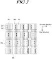
- FIG. 3 is a diagram illustrating the touch sensor employed in the touch display device illustrated in FIG. 1 .
- a plurality of touch electrodes TE, and a plurality of touch electrode lines Tel connected to each touch electrode TE are disposed on the display panel 110.
- the plurality of touch electrodes TE can be disposed to be spaced apart from one another.
- the plurality of touch electrodes TE is disposed such that 16 touch electrodes are disposed in a matrix form of 4*4, but embodiments of the present disclosure are not limited thereto.
- Each of the plurality of touch electrode lines Tel can extend in a first direction.
- the first touch electrode TE1 can correspond to the first cathode electrode 125a illustrated in FIG.
- Each touch electrode TE can be connected to a different touch electrode line TEL from one another.
- one touch electrode line TEL contacts one touch electrode TE at two points ct1 and ct2, but embodiments of the present disclosure are not limited thereto.
- One touch electrode line TEL can be contacted one touch electrode TE at one point ct1 or at two or more points.
- the two points ct1 and ct2 may be points at which the touch metal 121b illustrated in FIG. 2 is connected to the touch electrode TE.
- the first spacer 123a illustrated in FIG 2 can be disposed between the touch electrodes TE. That is, the first spacer 123a can be disposed in an area SA in which the touch electrode TE is not disposed. Accordingly, the area SA in which the touch electrode TE is not disposed can extend in a first direction and in a second direction, between the touch electrodes TE. Further, a plurality of pixels 101 can correspond to one touch electrode TE. That is, a plurality of organic light emitting diodes can be disposed under one touch electrode TE.
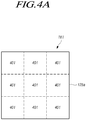
- FIG. 4A is a diagram illustrating an example of the touch electrode illustrated in FIG. 3
- FIG. 4B is a diagram illustrating another example of the touch electrode illustrated in FIG. 3 .
- the first cathode electrode 125a can be disposed to be corresponded to one first touch electrode TE1. That is, the first cathode electrode 125a can correspond to the first touch electrode TE1 illustrated in FIG. 2 .
- each of a plurality of boxes 401 represented by dotted lines in the first cathode electrode TE1 can correspond to each pixel 101. Accordingly, the plurality of pixels 101 can be corresponded to the first cathode electrode 125a.
- the first cathode electrode 125a is formed of one electrode body corresponding to the plurality of pixels 101; therefore can function as both a cathode electrode and a touch electrode being corresponded to the plurality of pixels 101.
- the first touch electrode TE1 can include a plurality of divided cathode electrodes 410 to 490 disposed in pixel areas.
- the plurality of divided cathode electrodes 410 to 490 disposed in the pixel areas can correspond to the first cathode electrode 125a illustrated in FIG. 2 .
- One 410 of the divided cathode electrodes 410 to 490 can directly contact the touch metal 121b.
- a part of one of the divided cathode electrodes 410 to 490 disposed in the pixel areas can be connected to a part of another one of the divided cathode electrodes 410 to 490 through a connection electrode AR.
- the connection electrode AR can be formed of the same material as the cathode electrode.
- each of the plurality of divided cathode electrodes 410 to 490 disposed in the pixel areas can correspond to one pixel 101.
- a plurality of pixels may correspond to each of the plurality of divided cathode electrodes 410 to 490 disposed in the pixel areas.
- another spacer can be disposed between the plurality of divided cathode electrodes 410 to 490 disposed in the pixel areas, which correspond one touch electrode TE.
- a spacer may not be disposed in an area in which the connection electrode AR is disposed.
- the divided cathode electrodes 410 to 490 disposed in the pixel areas can be transparent electrodes. Further, the divided cathode electrodes 410 to 490 disposed in the pixel areas can be in the form of a mesh.
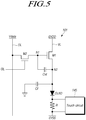
- FIG. 5 is a circuit diagram illustrating the subpixel employed in the display panel illustrated in FIG. 1 .
- the subpixel 101 can include: a first transistor M1 generating a first current in response to a data signal Vdata, a second transistor M2 transferring a data signal Vdata to the first transistor M1 in response to a gate signal, a storage capacitor Cst holding the data signal Vdata transferred to the first transistor M1, and an organic light emitting diode OLED emitting light by the first current received from the first transistor M1.
- the gate electrode of the first transistor M1 can be connected to a first node N1, and a first electrode thereof can be connected to a first power supply line VL1 to which a first power supply EVDD is supplied, and a second electrode thereof can be connected to a second node N2.
- the first electrode can be the source electrode illustrated in FIG 2
- the second electrode can be the drain electrode illustrated in FIG 2 .
- a magnitude of the first current can be determined corresponding to a voltage difference between the gate electrode and the second electrode of the first transistor M1.
- the gate electrode of the second transistor M2 can be connected to a gate line GL, and first and second electrodes thereof can be connected to a data line DL and the first node N1, respectively. Accordingly, a data signal flowing through the data line DL can be transferred to the first node N1 in response to a gate signal transferred through the gate line GL
- First and second electrodes of the storage capacitor Cst can be connected to the first and second nodes N1 and N2, respectively.
- the storage capacitor Cst can hole a voltage between the first node N1 and the second node N2. Accordingly, a voltage difference between the gate electrode and the second electrode of the first transistor M1 can be held during a certain interval, and the first current can therefore flow constantly.
- the organic light emitting diode OLED can emit light depending on a current supplied to the second node N2.
- the cathode electrode of the organic light emitting diode OLED can correspond to the cathode electrode 125a, 125b, 125c illustrated in FIG 2 .
- the touch circuit 145 can be connected to the cathode electrode of the organic light emitting diode OLED.
- the touch circuit 145 can detect the presence or non-presence of a touch using a magnitude of a current flowing corresponding to a magnitude of a resistance R connected between the cathode electrode of the organic light emitting diode and a second power supply EVSS.
- FIG. 6 is a timing chart illustrating a method of driving the display panel illustrated in FIG. 1
- FIG. 7 is a timing chart illustrating another method of driving the display panel illustrated in FIG. 1 .
- a synchronization signal Tsync can repeat a high state and a low state. During an interval in which the synchronization signal Tsync is in the low state, the display panel 110 can operates as a display interval, and the during an interval in which the synchronization signal Tsync is in the high state, the display panel 110 can operates as a touch interval.
- the synchronization signal Tsync can be divided into a first interval T1a corresponding to the interval in the low state and a second interval T2a corresponding to the interval in the high state.
- the first interval T1a and the second interval T2a can have an identical length, but embodiments of the present disclosure are not limited thereto.
- the second interval T2a can correspond to a vertical blank interval.
- the vertical blank interval may be a interval during which a vertical synchronizing signal is input, or may be a interval between one frame and the next frame.
- a data signal and a gate signal can be transferred to the data line DL and the gate line GL, respectively.
- the subpixel 101 illustrated in FIG. 5 can supply the first current to the organic light emitting diode OLED in response to the data signal, and then the organic light emitting diode OLED can emit light in response to the first current.
- DC voltages with predetermined values can be supplied from the first power supply EVDD and the second power supply EVSS.
- a voltage level of the first power supply EVDD may be greater than that of the second power supply EVSS.
- the voltage level of the first power supply EVDD may be 24V
- the voltage level of the second power supply EVSS may be 0V.
- embodiments of the present disclosure are not limited thereto.
- a voltage corresponding to a touch driving signal TDS can be transferred to the cathode electrode of the organic light emitting diode OLED.
- the touch driving signal TDS can include a plurality of pulses.
- a load free driving signal in synchronism with the touch driving signal TDS may be transferred to the first power supply EVDD.
- the load free driving signal may be transferred to a gate line GL and a data line DL.
- the load free driving signal in synchronism with the touch driving signal TDS is applied to the first power supply line VL1, the gate line GL and the data line DL, it is possible to prevent such a capacitance from being formed; therefore, it is possible to reduce the power consumption of the touch display device 100.
- the lines to which the load free driving signal is applied in the display panel 110 are not limited to the first power supply VL1, the gate line GL, and the data line DL.
- one frame period can be divided into a first interval T1b, a second interval T2b, a third interval T3b, and a fourth interval T4b.
- the synchronization signal Tsync can be in the low state
- the synchronization signal Tsync can be in the high state.
- all of the first interval to the fourth interval T1b to T4b can have an identical interval, as in IFG. 7, but embodiments of the present disclosure are not limited thereto.
- Each of the first interval to the fourth interval T1b to T4b may have a different length from one another.
- the second interval T2b and the fourth interval T4b can correspond to a vertical blank interval.
- the vertical blank interval may be a interval during which a vertical synchronizing signal is input, or may be a interval between one row and the next row of a plurality of rows of one frame.
- the second interval T2b and the fourth interval T4b can correspond to a long horizontal blank (LHB). 16 long horizontal blanks LHB may be disposed in one frame period.
- LHB long horizontal blank
- a data signal and a gate signal can be transferred to the data line DL and the gate line GL, respectively.
- the subpixel 101 illustrated in FIG. 5 can supply the first current to the organic light emitting diode OLED in response to the data signal, and then the organic light emitting diode OLED can emit light in response to the first current.
- DC voltages with predetermined values can be supplied from the first power supply EVDD and the second power supply EVSS.
- a voltage level of the first power supply EVDD may be greater than that of the second power supply EVSS.
- the voltage level of the first power supply EVDD may be 24V
- the voltage level of the second power supply EVSS may be 0V.
- embodiments of the present disclosure are not limited thereto.
- the touch display device can sequentially apply one or more touch driving signals through a touch electrode line TEL corresponding to each of a plurality of cathode electrodes which are electrically separated from one another of the organic light emitting diode OLED, and thus can sense the presence of a touch on the display panel.
- a load free driving signal may be applied to cathode electrodes which do not perform sensing.
- the load free driving signal and the touch driving signal are signals in synchronism with each other, and can be configured with an identical amplitude.
- a load free driving signal in synchronism with the touch driving signal TDS may be transferred to the first power supply EVDD.
- the load free driving signal may be transferred to a gate line GL and a data line DL.
- the lines to which the load free driving signal is applied in the display panel 110 are not limited thereto.
- FIG. 8 is a circuit diagram illustrating a connection between the touch circuit and the touch electrode illustrated in FIG. 5
- FIG. 9 is a graph illustrating the waveform of a signal applied to the touch circuit and the touch electrode illustrated in FIG. 8 .
- the touch circuit 145 can include an integrator 146 and a buffer 147.
- the integrator 146 can calculate a magnitude of a voltage charged in each cathode electrode in response to voltages corresponding to currents flowing by voltages charged in cathode electrodes 125a, 125b, and 125c which are electrically disconnected and a pre-set voltage.
- the buffer 147 can improve the characteristics of a voltage output from the integrator 146.
- the buffer 147 can include a first inverter 147a and a second inverter 147b. However, embodiments of the present disclosure are not limited thereto.
- the touch circuit 145 can be connected to a power supply line connected to the second power supply EVSS.
- the touch circuit 145 can be connected to the cathode electrode of the organic light emitting diode OLED through a touch line TEL.
- the organic light emitting diode OLED can be connected to a pixel circuit 1011 generating a first current.
- a touch capacitor Cf formed by a touch can be connected to the cathode electrode.
- a signal applying unit 148 for applying a voltage corresponding to the load free driving signal can be disposed in the cathode electrode.
- the load free driving signal is not applied to the first power supply line VL1 for supplying the first power supply EVDD, the data line DL, and the gate line GL, and a load free driving signal is applied by the signal applying unit 148 to the touch capacitor Cf instead of supplying a touch driving signal TDS to the cathode electrode.
- a magnitude of the touch capacitor Cf is represented by 1pF or 0.5pF. That is, it can be seen that a magnitude of the output voltage of the touch circuit is different depending on the magnitude of the touch capacitor Cf. Accordingly, it can be seen that a touch can be detected using changes in capacitance caused by a touch.
Landscapes
- Engineering & Computer Science (AREA)
- General Engineering & Computer Science (AREA)
- Theoretical Computer Science (AREA)
- Physics & Mathematics (AREA)
- Human Computer Interaction (AREA)
- General Physics & Mathematics (AREA)
- Microelectronics & Electronic Packaging (AREA)
- Optics & Photonics (AREA)
- Geometry (AREA)
- Electroluminescent Light Sources (AREA)
- Devices For Indicating Variable Information By Combining Individual Elements (AREA)
- Control Of El Displays (AREA)
Applications Claiming Priority (1)
| Application Number | Priority Date | Filing Date | Title |
|---|---|---|---|
| KR1020180172867A KR102688299B1 (ko) | 2018-12-28 | 2018-12-28 | 터치표시장치 |
Publications (2)
| Publication Number | Publication Date |
|---|---|
| EP3674858A2 true EP3674858A2 (de) | 2020-07-01 |
| EP3674858A3 EP3674858A3 (de) | 2020-08-26 |
Family
ID=68917524
Family Applications (1)
| Application Number | Title | Priority Date | Filing Date |
|---|---|---|---|
| EP19216408.5A Ceased EP3674858A3 (de) | 2018-12-28 | 2019-12-16 | Berührungsanzeigevorrichtung |
Country Status (5)
| Country | Link |
|---|---|
| US (2) | US11315986B2 (de) |
| EP (1) | EP3674858A3 (de) |
| JP (1) | JP6883642B2 (de) |
| KR (1) | KR102688299B1 (de) |
| CN (1) | CN111384116B (de) |
Cited By (1)
| Publication number | Priority date | Publication date | Assignee | Title |
|---|---|---|---|---|
| EP4024173A1 (de) * | 2020-12-31 | 2022-07-06 | LG Display Co., Ltd. | Berührungsanzeigevorrichtung und verfahren zur ansteuerung davon |
Families Citing this family (18)
| Publication number | Priority date | Publication date | Assignee | Title |
|---|---|---|---|---|
| CN113632590B (zh) * | 2019-03-28 | 2024-11-22 | 夏普株式会社 | 显示元件 |
| CN114115572A (zh) * | 2020-08-26 | 2022-03-01 | 深圳市柔宇科技股份有限公司 | 触控显示面板、其制作方法及电子设备 |
| KR102812266B1 (ko) * | 2020-10-28 | 2025-05-22 | 엘지디스플레이 주식회사 | 발광표시패널 및 이를 이용한 발광표시장치 |
| KR102890709B1 (ko) | 2020-12-11 | 2025-11-25 | 엘지디스플레이 주식회사 | 터치센서를 포함하는 표시장치 및 그의 제조방법 |
| KR102773867B1 (ko) * | 2020-12-18 | 2025-02-26 | 엘지디스플레이 주식회사 | 표시 장치 |
| KR102839630B1 (ko) * | 2020-12-30 | 2025-07-28 | 엘지디스플레이 주식회사 | 표시 장치 |
| JP7289903B2 (ja) * | 2020-12-31 | 2023-06-12 | エルジー ディスプレイ カンパニー リミテッド | 透明タッチディスプレイ装置 |
| KR102741708B1 (ko) | 2020-12-31 | 2024-12-12 | 엘지디스플레이 주식회사 | 터치 디스플레이 장치 |
| KR102862794B1 (ko) * | 2020-12-31 | 2025-09-22 | 엘지디스플레이 주식회사 | 터치 디스플레이 장치 |
| KR102757478B1 (ko) * | 2020-12-31 | 2025-01-20 | 엘지디스플레이 주식회사 | 터치 디스플레이 장치 |
| KR102820793B1 (ko) * | 2020-12-31 | 2025-06-13 | 엘지디스플레이 주식회사 | 터치 디스플레이 장치 |
| KR102811768B1 (ko) * | 2020-12-31 | 2025-05-22 | 엘지디스플레이 주식회사 | 터치 디스플레이 장치 |
| CN112864218A (zh) * | 2021-04-16 | 2021-05-28 | 京东方科技集团股份有限公司 | 发光基板和发光装置 |
| KR20230016731A (ko) | 2021-07-26 | 2023-02-03 | 삼성디스플레이 주식회사 | 표시 장치 |
| KR20230072565A (ko) | 2021-11-17 | 2023-05-25 | 삼성디스플레이 주식회사 | 표시장치 |
| US11861091B2 (en) | 2021-12-20 | 2024-01-02 | Lg Display Co., Ltd. | Display device |
| JP2023132064A (ja) * | 2022-03-10 | 2023-09-22 | 株式会社ジャパンディスプレイ | 表示装置及び表示装置の製造方法 |
| JP2023163756A (ja) * | 2022-04-28 | 2023-11-10 | 株式会社ジャパンディスプレイ | 表示装置及び表示装置の製造方法 |
Citations (1)
| Publication number | Priority date | Publication date | Assignee | Title |
|---|---|---|---|---|
| US20180150177A1 (en) * | 2016-10-31 | 2018-05-31 | Lg Display Co., Ltd. | Touch display device, touch driving circuit, and touch sensing method |
Family Cites Families (33)
| Publication number | Priority date | Publication date | Assignee | Title |
|---|---|---|---|---|
| KR20090109426A (ko) * | 2008-04-15 | 2009-10-20 | 삼성전자주식회사 | 디스플레이장치 및 그 제어방법 |
| JP5565047B2 (ja) * | 2010-03-31 | 2014-08-06 | 大日本印刷株式会社 | 有機エレクトロルミネッセンス素子およびその製造方法 |
| KR101719587B1 (ko) * | 2010-10-29 | 2017-03-27 | 삼성디스플레이 주식회사 | 터치 스크린 기능을 구비한 유기전계발광 표시장치 |
| KR101661015B1 (ko) * | 2013-11-28 | 2016-09-28 | 엘지디스플레이 주식회사 | 대면적 유기발광 다이오드 표시장치 |
| KR102174817B1 (ko) * | 2013-12-02 | 2020-11-05 | 엘지디스플레이 주식회사 | 터치센서 일체형 표시장치 |
| WO2015174683A1 (en) * | 2014-05-12 | 2015-11-19 | Lg Innotek Co., Ltd. | Touch window |
| EP3153956B1 (de) * | 2014-05-30 | 2020-05-06 | BOE Technology Group Co., Ltd. | Kapazitive berührungsstruktur, eingebetteter berührungsbildschirm, anzeigevorrichtung und abtastverfahren dafür |
| US9570471B2 (en) * | 2014-08-05 | 2017-02-14 | Lg Display Co., Ltd. | Organic light emitting display device and method of manufacturing the same |
| KR101679977B1 (ko) * | 2015-05-29 | 2016-11-28 | 엘지디스플레이 주식회사 | 자기 정전용량식 터치 센서 일체형 표시장치와 그 제조방법 |
| CN105094491B (zh) * | 2015-08-24 | 2018-04-20 | 京东方科技集团股份有限公司 | 触控显示面板及其制作方法、驱动方法和触控显示装置 |
| KR102438247B1 (ko) * | 2015-09-07 | 2022-08-30 | 엘지디스플레이 주식회사 | 유기 발광 표시 장치 및 이의 제조 방법 |
| CN105045435B (zh) * | 2015-09-11 | 2018-03-30 | 京东方科技集团股份有限公司 | 一种内嵌式触摸屏及显示装置 |
| KR102510915B1 (ko) * | 2015-09-16 | 2023-03-17 | 삼성디스플레이 주식회사 | 표시 장치 및 이의 제조 방법 |
| CN105139804B (zh) * | 2015-09-28 | 2018-12-21 | 京东方科技集团股份有限公司 | 一种像素驱动电路、显示面板及其驱动方法和显示装置 |
| US20170090615A1 (en) * | 2015-09-30 | 2017-03-30 | Synaptics Incorporated | Two-dimensional absolute capacitance sensing using electrode guarding techniques |
| CN205353991U (zh) * | 2016-01-26 | 2016-06-29 | 上海天马微电子有限公司 | 一种有机发光触控显示面板及有机发光触控显示装置 |
| JP6938119B2 (ja) * | 2016-06-28 | 2021-09-22 | 株式会社ジャパンディスプレイ | 入力機能付き透明ディスプレイ |
| KR102543382B1 (ko) * | 2016-06-30 | 2023-06-13 | 엘지디스플레이 주식회사 | 구동 방법, 터치 센싱 회로, 표시패널 및 터치 표시 장치 |
| KR102596065B1 (ko) * | 2016-07-04 | 2023-11-01 | 삼성디스플레이 주식회사 | 유기발광 표시장치 및 이의 제조 방법 |
| TWI601279B (zh) * | 2016-08-22 | 2017-10-01 | 群創光電股份有限公司 | 發光二極體觸控顯示裝置 |
| EP3316092B1 (de) * | 2016-10-28 | 2020-05-13 | LG Display Co., Ltd. | Elektrolumineszente anzeigevorrichtung mit integriertem berührungssensor |
| CN108091670B (zh) * | 2016-11-22 | 2022-04-15 | 天马微电子股份有限公司 | 显示装置及其制造方法 |
| CN106653813B (zh) * | 2016-12-26 | 2019-01-22 | 武汉华星光电技术有限公司 | 一种基于oled的内置式触控显示面板 |
| US11635832B2 (en) * | 2017-02-17 | 2023-04-25 | Novatek Microelectronics Corp. | Method of driving touch panel and touch with display driver system using the same |
| CN107092388B (zh) * | 2017-04-12 | 2024-05-03 | 北京集创北方科技股份有限公司 | 触控显示装置及其驱动方法 |
| CN107168574A (zh) * | 2017-05-10 | 2017-09-15 | 京东方科技集团股份有限公司 | 一种oled触控显示面板、触控显示装置 |
| KR102491224B1 (ko) * | 2017-06-01 | 2023-01-20 | 엘지디스플레이 주식회사 | 터치표시장치 및 터치패널 |
| WO2018230440A1 (ja) * | 2017-06-14 | 2018-12-20 | シャープ株式会社 | 表示基板及び表示装置 |
| US20190157355A1 (en) * | 2017-11-22 | 2019-05-23 | Wuhan China Star Optoelectronics Semiconductor Display Technology Co. Ltd. | Touch screen panel and manufacturing method thereof |
| US10784326B2 (en) * | 2017-12-13 | 2020-09-22 | Wuhan China Star Optoelectronics Semiconductor Display Technology Co., Ltd. | OLED display panel and display device |
| CN207834302U (zh) * | 2018-01-11 | 2018-09-07 | 京东方科技集团股份有限公司 | 一种显示面板及显示装置 |
| CN109032403B (zh) * | 2018-07-03 | 2021-10-26 | 京东方科技集团股份有限公司 | 一种触控基板及其驱动方法、触控装置 |
| CN110211539B (zh) * | 2018-08-02 | 2021-04-27 | 京东方科技集团股份有限公司 | 像素驱动电路、像素驱动方法和触控显示装置 |
-
2018
- 2018-12-28 KR KR1020180172867A patent/KR102688299B1/ko active Active
-
2019
- 2019-12-11 CN CN201911266265.5A patent/CN111384116B/zh active Active
- 2019-12-16 EP EP19216408.5A patent/EP3674858A3/de not_active Ceased
- 2019-12-17 JP JP2019227453A patent/JP6883642B2/ja active Active
- 2019-12-24 US US16/726,609 patent/US11315986B2/en active Active
-
2022
- 2022-03-22 US US17/701,178 patent/US12284898B2/en active Active
Patent Citations (1)
| Publication number | Priority date | Publication date | Assignee | Title |
|---|---|---|---|---|
| US20180150177A1 (en) * | 2016-10-31 | 2018-05-31 | Lg Display Co., Ltd. | Touch display device, touch driving circuit, and touch sensing method |
Cited By (2)
| Publication number | Priority date | Publication date | Assignee | Title |
|---|---|---|---|---|
| EP4024173A1 (de) * | 2020-12-31 | 2022-07-06 | LG Display Co., Ltd. | Berührungsanzeigevorrichtung und verfahren zur ansteuerung davon |
| US11579717B2 (en) | 2020-12-31 | 2023-02-14 | Lg Display Co., Ltd. | Touch display device and method for driving the same |
Also Published As
| Publication number | Publication date |
|---|---|
| KR20200082355A (ko) | 2020-07-08 |
| US12284898B2 (en) | 2025-04-22 |
| CN111384116A (zh) | 2020-07-07 |
| EP3674858A3 (de) | 2020-08-26 |
| JP2020109634A (ja) | 2020-07-16 |
| US20200212116A1 (en) | 2020-07-02 |
| CN111384116B (zh) | 2023-09-29 |
| KR102688299B1 (ko) | 2024-07-25 |
| US20220216271A1 (en) | 2022-07-07 |
| JP6883642B2 (ja) | 2021-06-09 |
| US11315986B2 (en) | 2022-04-26 |
Similar Documents
| Publication | Publication Date | Title |
|---|---|---|
| EP3674858A2 (de) | Berührungsanzeigevorrichtung | |
| EP3331019B1 (de) | Anzeigevorrichtung | |
| US8810490B2 (en) | Display apparatus | |
| US11327610B2 (en) | Display device with touch sensor and method of manufacturing same | |
| WO2016206251A1 (zh) | 一种内嵌式触摸显示屏、其驱动方法及显示装置 | |
| US10976870B2 (en) | Display device with inorganic film and method of fabricating the same | |
| KR102410631B1 (ko) | Oled 표시 장치 | |
| US11740737B2 (en) | Touch display device, touch driving circuit and touch driving method thereof | |
| WO2016206224A1 (zh) | 一种内嵌式触摸显示屏、其驱动方法及显示装置 | |
| US10950193B2 (en) | Display apparatus with touch sensor | |
| US11177292B2 (en) | Display device | |
| US10761652B2 (en) | Touch panel, touch device and method of manufacturing touch panel | |
| KR102611016B1 (ko) | 터치표시장치 및 그의 구동방법 | |
| TWI879254B (zh) | 觸控顯示裝置 | |
| KR20220091080A (ko) | 발광표시장치 | |
| CN109407357B (zh) | 包括光电传感器单元的显示面板和使用其的显示装置 | |
| CN111048042B (zh) | 显示面板和显示装置 | |
| KR20240020113A (ko) | 터치 구동 회로 및 터치 디스플레이 장치 | |
| US20240090283A1 (en) | Touch Display Device and Display Panel | |
| KR20210067373A (ko) | 터치 표시장치 및 그의 제조방법 | |
| US12613591B2 (en) | Touch display device and touch driving method | |
| US20260073868A1 (en) | Pixel circuit and display apparatus including the same | |
| KR102896935B1 (ko) | 터치감지장치, 터치센서를 포함하는 표시장치 및 그의 구동방법 | |
| US20250284366A1 (en) | Display device and electronic device including display device | |
| US20220130334A1 (en) | Pixel circuit, display device including the same, and method of driving pixel circuit |
Legal Events
| Date | Code | Title | Description |
|---|---|---|---|
| PUAI | Public reference made under article 153(3) epc to a published international application that has entered the european phase |
Free format text: ORIGINAL CODE: 0009012 |
|
| STAA | Information on the status of an ep patent application or granted ep patent |
Free format text: STATUS: REQUEST FOR EXAMINATION WAS MADE |
|
| 17P | Request for examination filed |
Effective date: 20191216 |
|
| AK | Designated contracting states |
Kind code of ref document: A2 Designated state(s): AL AT BE BG CH CY CZ DE DK EE ES FI FR GB GR HR HU IE IS IT LI LT LU LV MC MK MT NL NO PL PT RO RS SE SI SK SM TR |
|
| AX | Request for extension of the european patent |
Extension state: BA ME |
|
| PUAL | Search report despatched |
Free format text: ORIGINAL CODE: 0009013 |
|
| AK | Designated contracting states |
Kind code of ref document: A3 Designated state(s): AL AT BE BG CH CY CZ DE DK EE ES FI FR GB GR HR HU IE IS IT LI LT LU LV MC MK MT NL NO PL PT RO RS SE SI SK SM TR |
|
| AX | Request for extension of the european patent |
Extension state: BA ME |
|
| RIC1 | Information provided on ipc code assigned before grant |
Ipc: H01L 27/32 20060101ALI20200720BHEP Ipc: G06F 3/044 20060101ALI20200720BHEP Ipc: G06F 3/041 20060101AFI20200720BHEP |
|
| RBV | Designated contracting states (corrected) |
Designated state(s): AL AT BE BG CH CY CZ DE DK EE ES FI FR GB GR HR HU IE IS IT LI LT LU LV MC MK MT NL NO PL PT RO RS SE SI SK SM TR |
|
| STAA | Information on the status of an ep patent application or granted ep patent |
Free format text: STATUS: EXAMINATION IS IN PROGRESS |
|
| 17Q | First examination report despatched |
Effective date: 20210604 |
|
| STAA | Information on the status of an ep patent application or granted ep patent |
Free format text: STATUS: THE APPLICATION HAS BEEN REFUSED |
|
| 18R | Application refused |
Effective date: 20230503 |