EP3673534B1 - Übergang von einer streifenleitung auf einen hohlleiter - Google Patents
Übergang von einer streifenleitung auf einen hohlleiter Download PDFInfo
- Publication number
- EP3673534B1 EP3673534B1 EP18758862.9A EP18758862A EP3673534B1 EP 3673534 B1 EP3673534 B1 EP 3673534B1 EP 18758862 A EP18758862 A EP 18758862A EP 3673534 B1 EP3673534 B1 EP 3673534B1
- Authority
- EP
- European Patent Office
- Prior art keywords
- waveguide
- substrate
- block
- transition
- stripline
- Prior art date
- Legal status (The legal status is an assumption and is not a legal conclusion. Google has not performed a legal analysis and makes no representation as to the accuracy of the status listed.)
- Active
Links
Images



Classifications
-
- H—ELECTRICITY
- H01—ELECTRIC ELEMENTS
- H01P—WAVEGUIDES; RESONATORS, LINES, OR OTHER DEVICES OF THE WAVEGUIDE TYPE
- H01P5/00—Coupling devices of the waveguide type
- H01P5/08—Coupling devices of the waveguide type for linking dissimilar lines or devices
- H01P5/10—Coupling devices of the waveguide type for linking dissimilar lines or devices for coupling balanced lines or devices with unbalanced lines or devices
- H01P5/107—Hollow-waveguide/strip-line transitions
-
- H—ELECTRICITY
- H01—ELECTRIC ELEMENTS
- H01P—WAVEGUIDES; RESONATORS, LINES, OR OTHER DEVICES OF THE WAVEGUIDE TYPE
- H01P5/00—Coupling devices of the waveguide type
- H01P5/08—Coupling devices of the waveguide type for linking dissimilar lines or devices
-
- H—ELECTRICITY
- H01—ELECTRIC ELEMENTS
- H01P—WAVEGUIDES; RESONATORS, LINES, OR OTHER DEVICES OF THE WAVEGUIDE TYPE
- H01P1/00—Auxiliary devices
- H01P1/02—Bends; Corners; Twists
- H01P1/022—Bends; Corners; Twists in waveguides of polygonal cross-section
- H01P1/025—Bends; Corners; Twists in waveguides of polygonal cross-section in the E-plane
-
- H—ELECTRICITY
- H01—ELECTRIC ELEMENTS
- H01P—WAVEGUIDES; RESONATORS, LINES, OR OTHER DEVICES OF THE WAVEGUIDE TYPE
- H01P3/00—Waveguides; Transmission lines of the waveguide type
- H01P3/02—Waveguides; Transmission lines of the waveguide type with two longitudinal conductors
- H01P3/08—Microstrips; Strip lines
-
- H—ELECTRICITY
- H01—ELECTRIC ELEMENTS
- H01P—WAVEGUIDES; RESONATORS, LINES, OR OTHER DEVICES OF THE WAVEGUIDE TYPE
- H01P3/00—Waveguides; Transmission lines of the waveguide type
- H01P3/12—Hollow waveguides
-
- H—ELECTRICITY
- H05—ELECTRIC TECHNIQUES NOT OTHERWISE PROVIDED FOR
- H05K—PRINTED CIRCUITS; CASINGS OR CONSTRUCTIONAL DETAILS OF ELECTRIC APPARATUS; MANUFACTURE OF ASSEMBLAGES OF ELECTRICAL COMPONENTS
- H05K1/00—Printed circuits
- H05K1/02—Details
- H05K1/0213—Electrical arrangements not otherwise provided for
- H05K1/0237—High frequency adaptations
-
- H—ELECTRICITY
- H05—ELECTRIC TECHNIQUES NOT OTHERWISE PROVIDED FOR
- H05K—PRINTED CIRCUITS; CASINGS OR CONSTRUCTIONAL DETAILS OF ELECTRIC APPARATUS; MANUFACTURE OF ASSEMBLAGES OF ELECTRICAL COMPONENTS
- H05K1/00—Printed circuits
- H05K1/02—Details
- H05K1/11—Printed elements for providing electric connections to or between printed circuits
- H05K1/115—Via connections; Lands around holes or via connections
Definitions
- the present invention relates to a transition from a stripline to a waveguide.
- the transition is made by the stripline being located on a substrate, wherein an upper side of the substrate has a metallized surface and the lower side of the substrate has a metal layer, wherein the upper side and the lower side are connected by vias, wherein the metallized surface on the upper side of the substrate functions at least partially as a waveguide wall.
- the publication DE 196 36 890 C1 describes a method that involves contacting a stripline with a web in the waveguide.
- the waveguide walls are contacted both above and below the substrate.
- this principle has the serious disadvantage that such transitions can only be located at the edge of a substrate.
- transitions can be flexibly implemented at any point on a substrate, so that the necessary cable routing can be achieved.
- Another advantage is that an optimized structure and improved performance are achieved.
- the stripline is contacted by a step-like structure connected to the waveguide near the metallized surface on the top side of the substrate.
- the structure is located within a metal or metallized block, and the block has a plurality of waveguide structures, wherein at least a plurality of vias, preferably directly, contact the block in a transition region.
- the block has a rectangular waveguide in which an electrical wave propagates, whereby the waveguide wave is continued within the block by means of a 90° bend, so that the metallized surface on the top of the substrate only functions as a waveguide wall in the transition region.
- the 90° bend is preferably perpendicular to the substrate.
- the block preferably has several layers, which are produced using milling technology and/or 3D printing technology and/or plastic injection molding processes. Furthermore, a transition can be produced using an embossing or die-casting or cold flow process with subsequent metallization.
- the stripline ends at the point where it is contacted by the structure connected to the waveguide.
- the block is usually made of metal or another material that is metallized and can be manufactured in various interconnected layers.
- the necessary design criteria such as adding radii and drafts or any design criteria can easily be provided for in the block.
- the step-like contact structure can also be designed in the form of one or more drafts.
- the high-frequency ground potential required for the microstrip line mode is transferred from a metal layer on the underside of the substrate to the metallized surface on the top of the substrate by connecting both surfaces with vias in the area of the step-like contact structure.
- the metallized surface on the substrate acts partially as the wall of the waveguide.
- the other waveguide walls are located in the block. They receive their high-frequency ground potential by some vias, which transfer the ground potential, directly contacting the block in the transition area. This structure ensures that transitions can be implemented flexibly at any point on the substrate.
- Fig. 2 shows the components of a transition that are located directly on the substrate 3. These are the microstrip line 2, a metallized area 8 on the substrate and a layer 4 with ground potential below the substrate 3.
- the microstrip line 2 has a widening at its end.
- the metallized area 8 on the substrate begins shortly before the end of the microstrip line, with an area that has no metallization between the metallized area and the end of the microstrip line. This area is referred to as the recess 10 of the metallized area.
- the metallized area 8 on the substrate 3 is connected to a layer 4 with ground potential, which is located below the substrate 3 , by means of vias 7 .
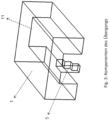
- Fig.3 shows a block 1 with a waveguide structure, which is located above the substrate.
- This has a rectangular recess 11 that is open at the bottom, in the transverse center of which the step-like contact structure 5 is located at the beginning of the recess.
- This preferably consists of three steps, whereby the structure increases in length towards an upper waveguide wall of the rectangular waveguide in the longitudinal direction of the waveguide. The lowest of the three steps contacts the microstrip line 2.
- areas of the block are marked which contact the vias on the metallized surface on the substrate.
- the step-like contact structure preferably consists of three steps, although it can also consist of any number of steps.
- a rectangular waveguide is obtained in the rectangular recess 11 , in which a transverse electrical wave, a TE10 wave, propagates.
- the rectangular waveguide is limited on three sides by the recess and from below by the metallized surface on the substrate. Since the transition should only take up a small amount of space on the substrate, it is necessary to continue the waveguide wave completely within the block.
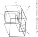
- Fig.4 shows an example of a continuation of the waveguide wave in a block.
- the wave can be guided exclusively in a block.
- On the side facing away from the step in the waveguide no metallized surface is required on the substrate.
- Fig.5 shows a very compact design of a transition, showing a block 1 with a waveguide structure, a metallized surface 8 on the substrate 3, a step-like contact structure, and a rectangular waveguide with H10 wave.
- the other components of the transition such as the microstrip line 2, the vias 7, the substrate 3 and the ground potential 4 below the substrate, remain in their arrangement according to Fig.1
- the compact variant is characterized by the fact that the 90° bend is located in the rear area of the block or directly on the opposite side of the step-like contact structure 5.
- the Fig.4 shown step in the waveguide 9 is in the compact construction according to Fig.5 not necessarily essential.
Landscapes
- Engineering & Computer Science (AREA)
- Microelectronics & Electronic Packaging (AREA)
- Waveguides (AREA)
- Structure Of Printed Boards (AREA)
Description
- Die vorliegende Erfindung betrifft einen Übergang von einer Streifenleitung auf einen Hohlleiter. Der Übergang erfolgt dadurch, dass sich die Streifenleitung auf einem Substrat befindet, wobei eine Oberseite des Substrates eine metallisierte Fläche und die Unterseite des Substrates eine Metallschicht aufweist, wobei die Oberseite und die Unterseite mit Durchkontaktierungen verbunden sind, wobei die metallisierte Fläche auf der Oberseite des Substrates zumindest teilweise als eine Hohlleiterwand fungiert.
- Aufgrund gesteigerter Anforderungen an die Sensorik wie zum Beispiel im Radarbereich gegeben durch die Zielsetzung des autonomen Fahrens, ergeben sich neue Herausforderungen in der Sensorentwicklung. Diese gesteigerten Ansprüche müssen dabei vor allem bei den Antennen der Sensoren berücksichtigt werden, da diese einen entscheidenden Einfluss auf das Gesamtsystem haben. Die derzeit häufig verwendeten planaren Antennen, die sich auf Leiterplatten befinden, können dabei oft nicht mehr die notwendige Leistung erbringen. Deshalb werden vermehrt Hohlleiterantennen eingesetzt. Da sich andere Sensorkomponenten, wie zum Beispiel Empfänger-und Sendechips, weiterhin auf Leiterplatten befinden, sind geeignete Übergänge zwischen Wellenführungen auf Leiterplatten und Wellenführungen in einem Hohlleiter entscheidende Komponenten vieler neuer Sensorsysteme.
- Ein Übergang wird beschrieben in: THOMAS J MULLER ET AL: "Surface-mountable metalized plastic waveguide filter suitable for high volume production", EUROPEAN MICROWAVE CONFERENCE 2003. 33RD, 1EEE, PISCATAWAY, NJ, USA, 1. Oktober 2003 (2003-10-01), S. 1255-1258.
- Weitere Übergänge von einer Streifenleitung auf einen Hohlleiter werden beispielsweise in
US 2002/163397 A1 ,JP H05 273234 A DE 197 25 492 C1 ,DE 10 2015 225496 A1 sowieDE 102 43 671 B3 beschrieben. - Die Druckschrift
DE 196 36 890 C1 beschreibt ein Verfahren, das eine Kontaktierung einer Streifenleitung mit einem im Hohlleiter befindlichen Steg beinhaltet. Die Kontaktierung der Hohlleiterwände erfolgt dabei sowohl oberhalb als auch unterhalb des Substrates. Dieses Prinzip hat jedoch den gravierenden Nachteil, dass sich solche Übergänge nur am Rand eines Substrates befinden können. - Aufgrund der gesteigerten Anforderungen an die Sensorsysteme ist es zukünftig notwendig Übergänge auf dem Substrat zu verteilen.
- Es ist deshalb eine Aufgabe der vorliegenden Erfindung, einen Übergang von einer Streifenleitung auf einen Hohlleiter bereitzustellen, welcher die im Stand der Technik vorhandenen Nachteile beseitigt oder vermindert und eine notwendige Leitungsführung realisiert.
- Die genannte Aufgabe wird gemäß den Merkmalen des unabhängigen Patentanspruchs 1 gelöst.
- Ein Vorteil ist dabei, dass die Übergänge flexibel an beliebigen Stellen auf einem Substrat realisiert werden können, so dass notwendige Leitungsführungen erreicht werden. Ein weiterer Vorteil ist, dass ein optimierter Aufbau und eine verbesserte Leistung realisiert werden.
- Bevorzugte oder vorteilhafte Ausführungsformen der Erfindung ergeben sich aus den Unteransprüchen, der nachfolgenden Beschreibung sowie den beigefügten Figuren.
- Bevorzugt wird die Streifenleitung von einer mit dem Hohlleiter verbundenen stufenartigen Struktur in der Nähe der metallisierten Fläche auf der Oberseite des Substrates kontaktiert.
- Die Struktur befindet sich innerhalb eines aus Metall bestehenden oder metallisierten Blockes, und der Block weist mehrere Hohlleiterstrukturen auf, wobei zumindest mehrere Durchkontaktierungen, vorzugsweise direkt, den Block in einem Übergangsbereich kontaktieren.
- Der Block weist einen Rechteckhohlleiter auf, in der sich eine elektrische Welle ausbreitet, wobei die Hohlleiterwelle innerhalb des Blockes mittels eines 90°-Knickes weitergeführt wird, so dass die metallisierte Fläche auf der Oberseite des Substrates lediglich in dem Übergangsbereich als Hohlleiterwand fungiert.
- Der 90°-Knick befindet sich bevorzugt senkrecht zum Substrat.
- Bevorzugt weist der Block mehrere Schichten auf, welche mittels Frästechnik und/oder 3D Drucktechnik und/oder Kunststoff-Spritzgussverfahren hergestellt werden. Ferner kann ein Übergang mittels eines Präge- oder Druckguss- oder Kaltfliessprozess mit anschließender Metallisierung hergestellt werden.
- Bevorzugt endet die Streifenleitung an der Stelle, an der sie durch die mit dem Hohlleiter verbundene Struktur kontaktiert wird.
- Der Block besteht üblicherweise aus Metall oder aus einem anderen Material, das metallisiert ist, und in verschiedenen miteinander verbundenen Schichten hergestellt werden kann. Die notwendigen Designkriterien wie das Hinzufügen von Radien und Formschrägen oder etwaige Designkriterien können bei dem Block problemlos vorgesehen werden. Des Weiteren kann die stufenartige Kontaktstruktur auch in Form einer oder mehrerer Schrägen ausgeführt werden.
- Weitere Merkmale, Vorteile und Wirkungen der Erfindung ergeben sich aus der nachfolgenden Beschreibung von Ausführungsbeispielen sowie der beigefügten Figuren. Dabei zeigen:
-
Fig. 1 einen prinzipiellen Aufbau eines Übergangs; -
Fig. 2 Komponenten eines Übergangs, die sich direkt an einem Substrat befinden; -
Fig. 3 Komponenten eines Übergangs, die sich innerhalb eines Blockes befinden; -
Fig. 4 eine beispielshafte Weiterführung der Hohlleiterwelle in einem Block; und -
Fig. 5 eine kompakte Ausführung eines Übergangs, wobei ausschließlich ein Block mit einer Hohlleiterstruktur und eine Massefläche auf einem Substrat dargestellt sind. -
Fig. 1 zeigt einen prinzipiellen Aufbau eines Übergangs, welcher aus einer Mikrostreifenleitung besteht. Die Mikrostreifenleitung 2 befindet sich auf einem Substrat 3. Unterhalb des Substrates befindet sich eine Schicht 4 mit Hochfrequenz-Massepotential. Somit bildet sich der bekannte Grundmode der Mikrostreifenleitung 2, ein sogenannter Quasi-Transversalelektromagnetischer (Quasi-TEM) Mode, aus. Anschließend wird die Mikrostreifenleitung 2 von einer stufenartigen Struktur 5 kontaktiert. Der Mikrostreifenleitungsmode wird somit in einem H10-Rechteckhohlleitermode 6 transformiert. Die stufenartige Kontaktstruktur 5 befindet sich innerhalb eines Blockes 1, der alle Hohlleiterstrukturen beinhaltet. Die Kontaktstruktur 5 ist mit einer Hohleiterwand verbunden. Somit besteht der Übergang gemäßFig. 1 aus: - einem Block 1 mit Hohlleiterstrukturen,
- einer Rechteckhohlleiter 6 mit H10-Welle,
- einer metallisierten Fläche 8 auf dem Substrat,
- Durchkontaktierungen (Vias) 7,
- einer Schicht 4 mit Massepotential,
- einem Substrat 3,
- einer Mikrostreifenleitung 2 mit Welle im Grundmode, und
- einer stufenartige Struktur 5, die die Mikrostreifenleitung kontaktiert.
- Das für den Mikrostreifenleitungsmode benötigte Hochfrequenz-Massepotential wird von einer Metallschicht auf der Unterseite des Substrates auf die metallisierte Fläche auf der Oberseite des Substrates übergeben, indem beide Flächen mit Durchkontaktierungen im Bereich der stufenartigen Kontaktstruktur verbunden sind. Die metallisierte Fläche auf dem Substrat fungiert dabei teilweise als Wand des Hohlleiters. Die anderen Hohlleiterwände befinden sich in dem Block. Deren Hochfrequenz-Massepotential erhalten sie dadurch, dass einige Durchkontaktierungen, die das Massepotential übergeben, direkt den Block im Übergangsbereich kontaktieren. Aufgrund dieses Aufbaus wird gewährleistet, dass flexibel an beliebigen Stellen auf dem Substrat Übergänge realisiert werden können.
-
Fig. 2 zeigt die Komponenten eines Übergangs, die sich direkt an dem Substrat 3 befinden. Diese sind die Mikrostreifenleitung 2, eine metallisierte Fläche 8 auf dem Substrat und eine Schicht 4 mit Massepotential unterhalb des Substrates 3. Dabei weist die Mikrostreifenleitung 2 an deren Ende eine Verbreiterung auf. Die metallisierte Fläche 8 auf dem Substrat beginnt kurz vor dem Ende der Mikrostreifenleitung, wobei sich zwischen der metallisierten Fläche und dem Ende der Mikrostreifenleitung, eine Fläche befindet, die keine Metallisierung aufweist. Dieser Bereich wird als Aussparung 10 der metallisierten Fläche bezeichnet. Entlang dieser Aussparung 10 ist die metallisierte Fläche 8 auf dem Substrat 3 mit einer Schicht 4 mit Massepotential, das sich unterhalb des Substrates 3 befindet, mittels Durchkontaktierungen (Vias) 7 verbunden. -
Fig. 3 zeigt einen Block 1 mit Hohlleiterstruktur, der sich oberhalb des Substrates befindet. Dieser weist eine rechteckförmige, nach unten offene Aussparung 11 auf, in dessen Quermitte sich am Beginn der Aussparung die stufenartige Kontaktstruktur 5 befindet. Diese besteht aus vorzugsweise drei Stufen, wobei die Struktur zu einer oberen Hohlleiterwand des Rechteckhohlleiters in Längsrichtung des Hohlleiters an Länge zunimmt. Die unterste der drei Stufen kontaktiert dabei die Mikrostreifenleitung 2. Des Weiteren sind Bereiche des Blockes gekennzeichnet, die die Durchkontaktierungen auf der metallisierten Fläche auf dem Substrat kontaktieren. Die stufenartige Kontaktstruktur besteht aus vorzugsweise drei Stufen, wobei sie jedoch auch aus einer beliebigen Anzahl von Stufen bestehen kann. - Im hinteren Bereich des Blockes beziehungsweise auf der abgewandten Seite der Kontaktstruktur erhält man in der rechteckförmigen Aussparung 11 einen Rechteckhohlleiter, in der sich eine transversal elektrische Welle, eine TE10-Welle, ausbreitet. Der Rechteckhohlleiter ist von drei Seiten durch die Aussparung und von unten durch die metallisierte Fläche auf dem Substrat begrenzt. Da der Übergang nur einen geringen Platz auf dem Substrat einnehmen soll, ist es notwendig die Hohlleiterwelle komplett innerhalb des Blockes weiterzuführen.
-
Fig. 4 zeigt eine beispielshafte Weiterführung der Hohlleiterwelle in einem Block. Mittels eines 90°-Knickes des Hohlleiters, der eine Stufe 9 aufweist, kann die Welle ausschließlich in einem Block geführt werden. Auf der abgewandten Seite der Stufe in dem Hohlleiter ist auf dem Substrat keine metallisierte Fläche mehr notwendig. Vor der Stufe in dem Hohlleiter besteht jedoch eine metallisierte Fläche 8 auf dem Substrat. Somit stelltFig. 4 die Weiterführung der Hohlleiterwelle in dem Block mittels Rechteckhohlleiter 6 mit H10-Welle im vorderen und hinterem Bereich des Blockes dar, wobei der vordere Bereich des Blockes eine metallisierte Fläche 8 auf dem Substrat aufweist, und eine Stufe im Hohlleiter 9 zum hinteren Bereich führt. -
Fig. 5 zeigt eine sehr kompakte Ausführung eines Übergangs, wobei ein Block 1 mit einer Hohlleiterstruktur, eine metallisierte Fläche 8 auf dem Substrat 3, eine stufenartige Kontaktstruktur, und ein Rechteckhohlleiter mit H10-Welle dargestellt sind. Die anderen Komponenten des Übergangs, wie die Mikrostreifenleitung 2, die Durchkontaktierungen 7, das Substrat 3 und das Massepotential 4 unterhalb des Substrates bleiben dabei in ihrer Anordnung entsprechendFig. 1 erhalten. Die kompakte Variante zeichnet sich dadurch aus, dass sich der 90°-Knick im hinteren Bereich des Blockes beziehungsweise direkt auf der abgewandten Seite der stufenartigen Kontaktstruktur 5 befindet. Die inFig. 4 gezeigte Stufe in dem Hohlleiter 9 ist bei dem kompakten Aufbau gemäßFig. 5 nicht zwangsläufig wesentlich. -
- 1
- Block mit Hohlleiterstrukturen
- 2
- Mikrostreifenleitung mit Welle im Grundmode
- 3
- Substrat
- 4
- Schicht mit Massepotential
- 5
- Stufenartige Kontaktstruktur
- 6
- Rechteckhohlleiter mit H10-Welle
- 7
- Durchkontaktierungen (Vias)
- 8
- Metallisierte Fläche auf dem Substrat
- 9
- Stufe im Hohlleiter
- 10
- Aussparung der metallisierten Fläche
- 11
- Rechteckförmige Aussparung
Claims (5)
- Übergang von einer Streifenleitung auf einen Hohlleiter, wobei sich die Streifenleitung, bevorzugt eine Mikrostreifenleitung (2), auf einem Substrat (3) befindet, wobei eine Oberseite des Substrates eine metallisierte Fläche (8) und die Unterseite des Substrates eine Metallschicht, bevorzugt eine Hochfrequenz-Massepotential-Schicht (4), aufweist, wobei die Oberseite und die Unterseite mit Durchkontaktierungen (7) verbunden sind,wobei die metallisierte Fläche auf der Oberseite des Substrates zumindest teilweise als eine Hohlleiterwand fungiert,wobei die Streifenleitung von einer mit dem Hohlleiter verbundenen stufenartigen Struktur (5) kontaktiert wird, die sich innerhalb eines aus Metall bestehenden oder metallisierten Blockes (l) befindet, wobei der Block mehrere Hohlleiterstrukturen aufweist, und wobei in einem Übergangsbereich mehrere Durchkontaktierungen den Block kontaktieren,wobeider Block einen Rechteckhohlleiter (6) aufweist, der eine elektrische Welle ausbreitet, wobei die Hohlleiterwelle innerhalb des Blocks mittels eines 90 0 -Knickes weitergeführt wird, der sich direkt auf der abgewandten Seite der stufenartigen Struktur (5) befindet, so dass die metallisierte Fläche auf der Oberseite des Substrats lediglich in dem Übergangsbereich als Hohlleiterwand fungiert.
- Übergang nach Anspruch l, wobei die Streifenleitung in der Nähe der metallisierten Fläche auf der Oberseite des Substrats von der stufenartigen Struktur kontaktiert wird.
- Übergang nach Anspruch 1 und 2, wobei im Übergangsbereich mehrere Durchkontaktierungen den Block direkt kontaktieren.
- Übergang nach Anspruch l, wobei sich der 90 0 -Knick senkrecht zum Substrat befindet
- Übergang nach einem der vorgehenden Ansprüche, wobei der Block mehrere Schichten aufweist, welche mittels Frästechnik und/oder 3D Drucktechnik und/oder Kunststoff-Spitzgussverfahren hergestellt werden
Applications Claiming Priority (2)
| Application Number | Priority Date | Filing Date | Title |
|---|---|---|---|
| DE102017214871.3A DE102017214871A1 (de) | 2017-08-24 | 2017-08-24 | Übergang von einer Streifenleitung auf einen Hohlleiter |
| PCT/EP2018/072450 WO2019038236A1 (de) | 2017-08-24 | 2018-08-20 | Übergang von einer streifenleitung auf einen hohlleiter |
Publications (2)
| Publication Number | Publication Date |
|---|---|
| EP3673534A1 EP3673534A1 (de) | 2020-07-01 |
| EP3673534B1 true EP3673534B1 (de) | 2024-07-31 |
Family
ID=63312013
Family Applications (1)
| Application Number | Title | Priority Date | Filing Date |
|---|---|---|---|
| EP18758862.9A Active EP3673534B1 (de) | 2017-08-24 | 2018-08-20 | Übergang von einer streifenleitung auf einen hohlleiter |
Country Status (7)
| Country | Link |
|---|---|
| US (1) | US11552379B2 (de) |
| EP (1) | EP3673534B1 (de) |
| JP (1) | JP7291121B2 (de) |
| KR (1) | KR102624788B1 (de) |
| CN (1) | CN111264000B (de) |
| DE (1) | DE102017214871A1 (de) |
| WO (1) | WO2019038236A1 (de) |
Families Citing this family (7)
| Publication number | Priority date | Publication date | Assignee | Title |
|---|---|---|---|---|
| EP3758137A1 (de) * | 2019-06-28 | 2020-12-30 | Nokia Solutions and Networks Oy | Struktur und verfahren zur herstellung einer struktur zur führung von elektromagnetischen wellen |
| TWI752780B (zh) * | 2020-12-31 | 2022-01-11 | 啓碁科技股份有限公司 | 寬波束之天線結構 |
| US11978954B2 (en) | 2021-06-02 | 2024-05-07 | The Boeing Company | Compact low-profile aperture antenna with integrated diplexer |
| CN113300094B (zh) * | 2021-06-29 | 2024-05-31 | 深圳金信诺高新技术股份有限公司 | 一种波导天线单元及波导阵列天线 |
| CN113782935B (zh) * | 2021-08-19 | 2022-10-25 | 北京古大仪表有限公司 | 微带-波导转换器和雷达物位计 |
| CN116435737A (zh) * | 2023-04-12 | 2023-07-14 | 北京遥感设备研究所 | 基于htcc工艺的亚毫米波三维传输结构及其工作方法 |
| KR102922285B1 (ko) * | 2024-10-25 | 2026-02-03 | 고려대학교 산학협력단 | 도파관-평판 선로 천이 구조체 |
Citations (1)
| Publication number | Priority date | Publication date | Assignee | Title |
|---|---|---|---|---|
| DE10243671B3 (de) * | 2002-09-20 | 2004-03-25 | Eads Deutschland Gmbh | Anordnung für einen Übergang zwischen einer Mikrostreifenleitung und einem Hohlleiter |
Family Cites Families (16)
| Publication number | Priority date | Publication date | Assignee | Title |
|---|---|---|---|---|
| JPH05273234A (ja) | 1992-03-25 | 1993-10-22 | Mitsubishi Electric Corp | Mmic装置及びrfプローブヘッド |
| JPH0634715A (ja) * | 1992-07-17 | 1994-02-10 | Mitsubishi Electric Corp | 高周波帯プローブヘッド |
| DE19636890C1 (de) | 1996-09-11 | 1998-02-12 | Bosch Gmbh Robert | Übergang von einem Hohlleiter auf eine Streifenleitung |
| DE19725492C1 (de) | 1997-06-17 | 1998-08-20 | Bosch Gmbh Robert | Anordnung zum Ankoppeln eines Rechteckhohlleiters an ein Speisenetzwerk einer planaren Antenne |
| US20020097108A1 (en) * | 2000-12-07 | 2002-07-25 | Nitin Jain | Transmission line to waveguide mode transformer |
| GB0108696D0 (en) | 2001-04-05 | 2001-05-30 | Koninkl Philips Electronics Nv | A transition from microstrip to waveguide |
| WO2008069714A1 (en) | 2006-12-05 | 2008-06-12 | Telefonaktiebolaget Lm Ericsson (Publ) | A surface-mountable waveguide arrangement |
| CN101677145A (zh) | 2008-09-17 | 2010-03-24 | 中国科学院微电子研究所 | 应用于微带-波导转换的阶梯型脊波导结构 |
| CN201266665Y (zh) | 2008-09-18 | 2009-07-01 | 成都雷电微力科技有限公司 | 毫米波t/r收发模块脊波导 |
| KR101055425B1 (ko) * | 2010-04-30 | 2011-08-08 | 삼성전기주식회사 | 광대역 전송선로-도파관 변환장치 |
| CN102074772B (zh) | 2011-01-07 | 2014-01-29 | 中国电子科技集团公司第十研究所 | 带状线-波导转换器 |
| JP2013243530A (ja) * | 2012-05-21 | 2013-12-05 | Mitsubishi Electric Corp | 導波管及びそれを用いた高周波モジュール |
| JP6417329B2 (ja) | 2013-10-01 | 2018-11-07 | ソニーセミコンダクタソリューションズ株式会社 | コネクタ装置及び通信システム |
| US9537199B2 (en) * | 2015-03-19 | 2017-01-03 | International Business Machines Corporation | Package structure having an integrated waveguide configured to communicate between first and second integrated circuit chips |
| DE102015225496A1 (de) | 2015-12-16 | 2017-06-22 | Airbus Defence and Space GmbH | Leiterplatte für HF-Anwendungen mit integrierter Breitbandantenne |
| KR102674456B1 (ko) * | 2017-01-26 | 2024-06-13 | 주식회사 케이엠더블유 | 전송선로-도파관 전이 장치 |
-
2017
- 2017-08-24 DE DE102017214871.3A patent/DE102017214871A1/de not_active Withdrawn
-
2018
- 2018-08-20 EP EP18758862.9A patent/EP3673534B1/de active Active
- 2018-08-20 US US16/640,782 patent/US11552379B2/en active Active
- 2018-08-20 JP JP2020509078A patent/JP7291121B2/ja active Active
- 2018-08-20 CN CN201880054938.8A patent/CN111264000B/zh active Active
- 2018-08-20 WO PCT/EP2018/072450 patent/WO2019038236A1/de not_active Ceased
- 2018-08-20 KR KR1020207005487A patent/KR102624788B1/ko active Active
Patent Citations (1)
| Publication number | Priority date | Publication date | Assignee | Title |
|---|---|---|---|---|
| DE10243671B3 (de) * | 2002-09-20 | 2004-03-25 | Eads Deutschland Gmbh | Anordnung für einen Übergang zwischen einer Mikrostreifenleitung und einem Hohlleiter |
Also Published As
| Publication number | Publication date |
|---|---|
| US20210036394A1 (en) | 2021-02-04 |
| KR20200040777A (ko) | 2020-04-20 |
| US11552379B2 (en) | 2023-01-10 |
| DE102017214871A1 (de) | 2019-02-28 |
| CN111264000B (zh) | 2023-02-17 |
| EP3673534A1 (de) | 2020-07-01 |
| WO2019038236A1 (de) | 2019-02-28 |
| JP2020532190A (ja) | 2020-11-05 |
| KR102624788B1 (ko) | 2024-01-12 |
| JP7291121B2 (ja) | 2023-06-14 |
| CN111264000A (zh) | 2020-06-09 |
Similar Documents
| Publication | Publication Date | Title |
|---|---|---|
| EP3673534A1 (de) | Übergang von einer streifenleitung auf einen hohlleiter | |
| DE69622066T2 (de) | Senkrecht verbindende Anordnung aus einer Leitung mit drei Drähten für Mehrebenensubstrate | |
| DE69620673T2 (de) | Senkrechte Mikrowellenverbindung mittels Anordnung mit kompressiblem Leiter | |
| DE69612322T2 (de) | H-geknickte Verbindungseinrichtung für vertikale geerdete koplanare Wellenleiter | |
| DE60208294T2 (de) | Übergangsstruktur zwischen einer Übertragungsleitung und einem Hohlleiter | |
| DE10243671B3 (de) | Anordnung für einen Übergang zwischen einer Mikrostreifenleitung und einem Hohlleiter | |
| DE2212735B2 (de) | Hochfrequenz-Übertragungsleitung in Streifenleiterbauweise | |
| DE102006041994B4 (de) | Wellenleiter/Streifenleiter-Wandler | |
| DE102014203185A1 (de) | Antennenvorrichtung und Radarvorrichtung | |
| DE60305553T2 (de) | Leistungsteiler/-kombinierer | |
| DE102011102484A1 (de) | Leiterplatte mit Formteil und Verfahren zu dessen Herstellung | |
| DE112018006818T5 (de) | Wellenleiter-mikrostreifenleitungs-wandler und antennenvorrichtung | |
| DE4120521A1 (de) | Mikrowellen-planarantenne fuer zwei orthogonale polarisationen mit einem paar von orthogonalen strahlerschlitzen | |
| DE102007054621A1 (de) | Hochfrequenzfilter mit elektromagnetisch gekoppelten Verzweigungsleitungen | |
| DE3340566C2 (de) | ||
| EP3293814B1 (de) | Schaltungssubstrat und elektronisches höchstfrequenz-bauteil | |
| DE102017216906A1 (de) | Wellenleitersystem, Hochfrequenzleitung und Radarsensor | |
| DE3416107A1 (de) | Busleitungsanordnung mit hoher kapazitaet in schichtbauweise | |
| WO2006105847A1 (de) | HOCHFREQUENZKOPPLER ODER LEISTUNGSTEILER, INSBESONDERE SCHMALBANDIGER UND/ODER 3dB-KOPPLER ODER LEISTUNGSTEILER | |
| DE10156341B4 (de) | Verdrahtungsaufbau für Übertragungsleitung | |
| DE69935615T2 (de) | Breitbaniger übergang von einem hohlleiter auf eine mikrostreifenleitung | |
| EP4449549A1 (de) | Hochfrequenzbaugruppe für radarsensoren | |
| DE69505860T2 (de) | Komparator | |
| DE3788018T2 (de) | Richtkoppler. | |
| DE19837025A1 (de) | Richtkoppler |
Legal Events
| Date | Code | Title | Description |
|---|---|---|---|
| STAA | Information on the status of an ep patent application or granted ep patent |
Free format text: STATUS: UNKNOWN |
|
| STAA | Information on the status of an ep patent application or granted ep patent |
Free format text: STATUS: THE INTERNATIONAL PUBLICATION HAS BEEN MADE |
|
| PUAI | Public reference made under article 153(3) epc to a published international application that has entered the european phase |
Free format text: ORIGINAL CODE: 0009012 |
|
| STAA | Information on the status of an ep patent application or granted ep patent |
Free format text: STATUS: REQUEST FOR EXAMINATION WAS MADE |
|
| 17P | Request for examination filed |
Effective date: 20200212 |
|
| AK | Designated contracting states |
Kind code of ref document: A1 Designated state(s): AL AT BE BG CH CY CZ DE DK EE ES FI FR GB GR HR HU IE IS IT LI LT LU LV MC MK MT NL NO PL PT RO RS SE SI SK SM TR |
|
| AX | Request for extension of the european patent |
Extension state: BA ME |
|
| DAV | Request for validation of the european patent (deleted) | ||
| DAX | Request for extension of the european patent (deleted) | ||
| STAA | Information on the status of an ep patent application or granted ep patent |
Free format text: STATUS: EXAMINATION IS IN PROGRESS |
|
| 17Q | First examination report despatched |
Effective date: 20220315 |
|
| P01 | Opt-out of the competence of the unified patent court (upc) registered |
Effective date: 20230526 |
|
| RIC1 | Information provided on ipc code assigned before grant |
Ipc: H01P 1/02 20060101ALI20240123BHEP Ipc: H01P 5/107 20060101AFI20240123BHEP |
|
| GRAP | Despatch of communication of intention to grant a patent |
Free format text: ORIGINAL CODE: EPIDOSNIGR1 |
|
| STAA | Information on the status of an ep patent application or granted ep patent |
Free format text: STATUS: GRANT OF PATENT IS INTENDED |
|
| INTG | Intention to grant announced |
Effective date: 20240305 |
|
| GRAS | Grant fee paid |
Free format text: ORIGINAL CODE: EPIDOSNIGR3 |
|
| GRAA | (expected) grant |
Free format text: ORIGINAL CODE: 0009210 |
|
| STAA | Information on the status of an ep patent application or granted ep patent |
Free format text: STATUS: THE PATENT HAS BEEN GRANTED |
|
| AK | Designated contracting states |
Kind code of ref document: B1 Designated state(s): AL AT BE BG CH CY CZ DE DK EE ES FI FR GB GR HR HU IE IS IT LI LT LU LV MC MK MT NL NO PL PT RO RS SE SI SK SM TR |
|
| REG | Reference to a national code |
Ref country code: CH Ref legal event code: EP Ref country code: GB Ref legal event code: FG4D Free format text: NOT ENGLISH |
|
| REG | Reference to a national code |
Ref country code: DE Ref legal event code: R096 Ref document number: 502018014951 Country of ref document: DE |
|
| REG | Reference to a national code |
Ref country code: IE Ref legal event code: FG4D Free format text: LANGUAGE OF EP DOCUMENT: GERMAN |
|
| REG | Reference to a national code |
Ref country code: DE Ref legal event code: R081 Ref document number: 502018014951 Country of ref document: DE Owner name: CRUISE MUNICH GMBH, DE Free format text: FORMER OWNER: ANMELDERANGABEN UNKLAR / UNVOLLSTAENDIG, 80297 MUENCHEN, DE Ref country code: DE Ref legal event code: R081 Ref document number: 502018014951 Country of ref document: DE Owner name: ASTYX GMBH, DE Free format text: FORMER OWNER: ANMELDERANGABEN UNKLAR / UNVOLLSTAENDIG, 80297 MUENCHEN, DE |
|
| REG | Reference to a national code |
Ref country code: DE Ref legal event code: R081 Ref document number: 502018014951 Country of ref document: DE Owner name: CRUISE MUNICH GMBH, DE Free format text: FORMER OWNER: ASTYX GMBH, 85521 OTTOBRUNN, DE |
|
| REG | Reference to a national code |
Ref country code: LT Ref legal event code: MG9D |
|
| REG | Reference to a national code |
Ref country code: NL Ref legal event code: MP Effective date: 20240731 |
|
| PG25 | Lapsed in a contracting state [announced via postgrant information from national office to epo] |
Ref country code: PT Free format text: LAPSE BECAUSE OF FAILURE TO SUBMIT A TRANSLATION OF THE DESCRIPTION OR TO PAY THE FEE WITHIN THE PRESCRIBED TIME-LIMIT Effective date: 20241202 |
|
| PG25 | Lapsed in a contracting state [announced via postgrant information from national office to epo] |
Ref country code: PT Free format text: LAPSE BECAUSE OF FAILURE TO SUBMIT A TRANSLATION OF THE DESCRIPTION OR TO PAY THE FEE WITHIN THE PRESCRIBED TIME-LIMIT Effective date: 20241202 |
|
| PG25 | Lapsed in a contracting state [announced via postgrant information from national office to epo] |
Ref country code: NO Free format text: LAPSE BECAUSE OF FAILURE TO SUBMIT A TRANSLATION OF THE DESCRIPTION OR TO PAY THE FEE WITHIN THE PRESCRIBED TIME-LIMIT Effective date: 20241031 |
|
| PG25 | Lapsed in a contracting state [announced via postgrant information from national office to epo] |
Ref country code: NL Free format text: LAPSE BECAUSE OF FAILURE TO SUBMIT A TRANSLATION OF THE DESCRIPTION OR TO PAY THE FEE WITHIN THE PRESCRIBED TIME-LIMIT Effective date: 20240731 Ref country code: FI Free format text: LAPSE BECAUSE OF FAILURE TO SUBMIT A TRANSLATION OF THE DESCRIPTION OR TO PAY THE FEE WITHIN THE PRESCRIBED TIME-LIMIT Effective date: 20240731 Ref country code: GR Free format text: LAPSE BECAUSE OF FAILURE TO SUBMIT A TRANSLATION OF THE DESCRIPTION OR TO PAY THE FEE WITHIN THE PRESCRIBED TIME-LIMIT Effective date: 20241101 Ref country code: PL Free format text: LAPSE BECAUSE OF FAILURE TO SUBMIT A TRANSLATION OF THE DESCRIPTION OR TO PAY THE FEE WITHIN THE PRESCRIBED TIME-LIMIT Effective date: 20240731 |
|
| PG25 | Lapsed in a contracting state [announced via postgrant information from national office to epo] |
Ref country code: BG Free format text: LAPSE BECAUSE OF FAILURE TO SUBMIT A TRANSLATION OF THE DESCRIPTION OR TO PAY THE FEE WITHIN THE PRESCRIBED TIME-LIMIT Effective date: 20240731 |
|
| PG25 | Lapsed in a contracting state [announced via postgrant information from national office to epo] |
Ref country code: LV Free format text: LAPSE BECAUSE OF FAILURE TO SUBMIT A TRANSLATION OF THE DESCRIPTION OR TO PAY THE FEE WITHIN THE PRESCRIBED TIME-LIMIT Effective date: 20240731 |
|
| PG25 | Lapsed in a contracting state [announced via postgrant information from national office to epo] |
Ref country code: IS Free format text: LAPSE BECAUSE OF FAILURE TO SUBMIT A TRANSLATION OF THE DESCRIPTION OR TO PAY THE FEE WITHIN THE PRESCRIBED TIME-LIMIT Effective date: 20241130 |
|
| PG25 | Lapsed in a contracting state [announced via postgrant information from national office to epo] |
Ref country code: HR Free format text: LAPSE BECAUSE OF FAILURE TO SUBMIT A TRANSLATION OF THE DESCRIPTION OR TO PAY THE FEE WITHIN THE PRESCRIBED TIME-LIMIT Effective date: 20240731 |
|
| PG25 | Lapsed in a contracting state [announced via postgrant information from national office to epo] |
Ref country code: RS Free format text: LAPSE BECAUSE OF FAILURE TO SUBMIT A TRANSLATION OF THE DESCRIPTION OR TO PAY THE FEE WITHIN THE PRESCRIBED TIME-LIMIT Effective date: 20241031 Ref country code: ES Free format text: LAPSE BECAUSE OF FAILURE TO SUBMIT A TRANSLATION OF THE DESCRIPTION OR TO PAY THE FEE WITHIN THE PRESCRIBED TIME-LIMIT Effective date: 20240731 |
|
| PG25 | Lapsed in a contracting state [announced via postgrant information from national office to epo] |
Ref country code: RS Free format text: LAPSE BECAUSE OF FAILURE TO SUBMIT A TRANSLATION OF THE DESCRIPTION OR TO PAY THE FEE WITHIN THE PRESCRIBED TIME-LIMIT Effective date: 20241031 Ref country code: PL Free format text: LAPSE BECAUSE OF FAILURE TO SUBMIT A TRANSLATION OF THE DESCRIPTION OR TO PAY THE FEE WITHIN THE PRESCRIBED TIME-LIMIT Effective date: 20240731 Ref country code: NO Free format text: LAPSE BECAUSE OF FAILURE TO SUBMIT A TRANSLATION OF THE DESCRIPTION OR TO PAY THE FEE WITHIN THE PRESCRIBED TIME-LIMIT Effective date: 20241031 Ref country code: NL Free format text: LAPSE BECAUSE OF FAILURE TO SUBMIT A TRANSLATION OF THE DESCRIPTION OR TO PAY THE FEE WITHIN THE PRESCRIBED TIME-LIMIT Effective date: 20240731 Ref country code: LV Free format text: LAPSE BECAUSE OF FAILURE TO SUBMIT A TRANSLATION OF THE DESCRIPTION OR TO PAY THE FEE WITHIN THE PRESCRIBED TIME-LIMIT Effective date: 20240731 Ref country code: IS Free format text: LAPSE BECAUSE OF FAILURE TO SUBMIT A TRANSLATION OF THE DESCRIPTION OR TO PAY THE FEE WITHIN THE PRESCRIBED TIME-LIMIT Effective date: 20241130 Ref country code: HR Free format text: LAPSE BECAUSE OF FAILURE TO SUBMIT A TRANSLATION OF THE DESCRIPTION OR TO PAY THE FEE WITHIN THE PRESCRIBED TIME-LIMIT Effective date: 20240731 Ref country code: GR Free format text: LAPSE BECAUSE OF FAILURE TO SUBMIT A TRANSLATION OF THE DESCRIPTION OR TO PAY THE FEE WITHIN THE PRESCRIBED TIME-LIMIT Effective date: 20241101 Ref country code: FI Free format text: LAPSE BECAUSE OF FAILURE TO SUBMIT A TRANSLATION OF THE DESCRIPTION OR TO PAY THE FEE WITHIN THE PRESCRIBED TIME-LIMIT Effective date: 20240731 Ref country code: ES Free format text: LAPSE BECAUSE OF FAILURE TO SUBMIT A TRANSLATION OF THE DESCRIPTION OR TO PAY THE FEE WITHIN THE PRESCRIBED TIME-LIMIT Effective date: 20240731 Ref country code: BG Free format text: LAPSE BECAUSE OF FAILURE TO SUBMIT A TRANSLATION OF THE DESCRIPTION OR TO PAY THE FEE WITHIN THE PRESCRIBED TIME-LIMIT Effective date: 20240731 |
|
| REG | Reference to a national code |
Ref country code: CH Ref legal event code: PL |
|
| PG25 | Lapsed in a contracting state [announced via postgrant information from national office to epo] |
Ref country code: DK Free format text: LAPSE BECAUSE OF FAILURE TO SUBMIT A TRANSLATION OF THE DESCRIPTION OR TO PAY THE FEE WITHIN THE PRESCRIBED TIME-LIMIT Effective date: 20240731 Ref country code: RO Free format text: LAPSE BECAUSE OF FAILURE TO SUBMIT A TRANSLATION OF THE DESCRIPTION OR TO PAY THE FEE WITHIN THE PRESCRIBED TIME-LIMIT Effective date: 20240731 Ref country code: SM Free format text: LAPSE BECAUSE OF FAILURE TO SUBMIT A TRANSLATION OF THE DESCRIPTION OR TO PAY THE FEE WITHIN THE PRESCRIBED TIME-LIMIT Effective date: 20240731 |
|
| PG25 | Lapsed in a contracting state [announced via postgrant information from national office to epo] |
Ref country code: LU Free format text: LAPSE BECAUSE OF NON-PAYMENT OF DUE FEES Effective date: 20240820 |
|
| PG25 | Lapsed in a contracting state [announced via postgrant information from national office to epo] |
Ref country code: EE Free format text: LAPSE BECAUSE OF FAILURE TO SUBMIT A TRANSLATION OF THE DESCRIPTION OR TO PAY THE FEE WITHIN THE PRESCRIBED TIME-LIMIT Effective date: 20240731 Ref country code: CH Free format text: LAPSE BECAUSE OF NON-PAYMENT OF DUE FEES Effective date: 20240831 Ref country code: MC Free format text: LAPSE BECAUSE OF FAILURE TO SUBMIT A TRANSLATION OF THE DESCRIPTION OR TO PAY THE FEE WITHIN THE PRESCRIBED TIME-LIMIT Effective date: 20240731 |
|
| PG25 | Lapsed in a contracting state [announced via postgrant information from national office to epo] |
Ref country code: CZ Free format text: LAPSE BECAUSE OF FAILURE TO SUBMIT A TRANSLATION OF THE DESCRIPTION OR TO PAY THE FEE WITHIN THE PRESCRIBED TIME-LIMIT Effective date: 20240731 |
|
| PG25 | Lapsed in a contracting state [announced via postgrant information from national office to epo] |
Ref country code: SK Free format text: LAPSE BECAUSE OF FAILURE TO SUBMIT A TRANSLATION OF THE DESCRIPTION OR TO PAY THE FEE WITHIN THE PRESCRIBED TIME-LIMIT Effective date: 20240731 Ref country code: IT Free format text: LAPSE BECAUSE OF FAILURE TO SUBMIT A TRANSLATION OF THE DESCRIPTION OR TO PAY THE FEE WITHIN THE PRESCRIBED TIME-LIMIT Effective date: 20240731 |
|
| REG | Reference to a national code |
Ref country code: DE Ref legal event code: R097 Ref document number: 502018014951 Country of ref document: DE |
|
| PLBE | No opposition filed within time limit |
Free format text: ORIGINAL CODE: 0009261 |
|
| STAA | Information on the status of an ep patent application or granted ep patent |
Free format text: STATUS: NO OPPOSITION FILED WITHIN TIME LIMIT |
|
| REG | Reference to a national code |
Ref country code: DE Ref legal event code: R082 Ref document number: 502018014951 Country of ref document: DE Representative=s name: MANITZ FINSTERWALD PATENT- UND RECHTSANWALTSPA, DE |
|
| GBPC | Gb: european patent ceased through non-payment of renewal fee |
Effective date: 20241031 |
|
| REG | Reference to a national code |
Ref country code: BE Ref legal event code: MM Effective date: 20240831 |
|
| 26N | No opposition filed |
Effective date: 20250501 |
|
| PG25 | Lapsed in a contracting state [announced via postgrant information from national office to epo] |
Ref country code: GB Free format text: LAPSE BECAUSE OF NON-PAYMENT OF DUE FEES Effective date: 20241031 |
|
| PG25 | Lapsed in a contracting state [announced via postgrant information from national office to epo] |
Ref country code: BE Free format text: LAPSE BECAUSE OF NON-PAYMENT OF DUE FEES Effective date: 20240831 |
|
| PG25 | Lapsed in a contracting state [announced via postgrant information from national office to epo] |
Ref country code: FR Free format text: LAPSE BECAUSE OF NON-PAYMENT OF DUE FEES Effective date: 20240930 |
|
| PG25 | Lapsed in a contracting state [announced via postgrant information from national office to epo] |
Ref country code: IE Free format text: LAPSE BECAUSE OF NON-PAYMENT OF DUE FEES Effective date: 20240820 |
|
| PG25 | Lapsed in a contracting state [announced via postgrant information from national office to epo] |
Ref country code: SE Free format text: LAPSE BECAUSE OF FAILURE TO SUBMIT A TRANSLATION OF THE DESCRIPTION OR TO PAY THE FEE WITHIN THE PRESCRIBED TIME-LIMIT Effective date: 20240731 |
|
| PGFP | Annual fee paid to national office [announced via postgrant information from national office to epo] |
Ref country code: DE Payment date: 20250827 Year of fee payment: 8 |
|
| REG | Reference to a national code |
Ref country code: AT Ref legal event code: MM01 Ref document number: 1709375 Country of ref document: AT Kind code of ref document: T Effective date: 20240820 |
|
| PG25 | Lapsed in a contracting state [announced via postgrant information from national office to epo] |
Ref country code: AT Free format text: LAPSE BECAUSE OF NON-PAYMENT OF DUE FEES Effective date: 20240820 |
|
| PG25 | Lapsed in a contracting state [announced via postgrant information from national office to epo] |
Ref country code: CY Free format text: LAPSE BECAUSE OF FAILURE TO SUBMIT A TRANSLATION OF THE DESCRIPTION OR TO PAY THE FEE WITHIN THE PRESCRIBED TIME-LIMIT; INVALID AB INITIO Effective date: 20180820 |
|
| PG25 | Lapsed in a contracting state [announced via postgrant information from national office to epo] |
Ref country code: HU Free format text: LAPSE BECAUSE OF FAILURE TO SUBMIT A TRANSLATION OF THE DESCRIPTION OR TO PAY THE FEE WITHIN THE PRESCRIBED TIME-LIMIT; INVALID AB INITIO Effective date: 20180820 |