EP3672382B1 - Presselement, montage und elektrische ausrüstung - Google Patents
Presselement, montage und elektrische ausrüstung Download PDFInfo
- Publication number
- EP3672382B1 EP3672382B1 EP19213473.2A EP19213473A EP3672382B1 EP 3672382 B1 EP3672382 B1 EP 3672382B1 EP 19213473 A EP19213473 A EP 19213473A EP 3672382 B1 EP3672382 B1 EP 3672382B1
- Authority
- EP
- European Patent Office
- Prior art keywords
- pressing member
- electrical
- pressing
- assembly
- electrical device
- Prior art date
- Legal status (The legal status is an assumption and is not a legal conclusion. Google has not performed a legal analysis and makes no representation as to the accuracy of the status listed.)
- Active
Links
Images


Classifications
-
- H—ELECTRICITY
- H05—ELECTRIC TECHNIQUES NOT OTHERWISE PROVIDED FOR
- H05K—PRINTED CIRCUITS; CASINGS OR CONSTRUCTIONAL DETAILS OF ELECTRIC APPARATUS; MANUFACTURE OF ASSEMBLAGES OF ELECTRICAL COMPONENTS
- H05K7/00—Constructional details common to different types of electric apparatus
- H05K7/20—Modifications to facilitate cooling, ventilating, or heating
- H05K7/2039—Modifications to facilitate cooling, ventilating, or heating characterised by the heat transfer by conduction from the heat generating element to a dissipating body
- H05K7/20436—Inner thermal coupling elements in heat dissipating housings, e.g. protrusions or depressions integrally formed in the housing
- H05K7/2049—Pressing means used to urge contact, e.g. springs
-
- H—ELECTRICITY
- H05—ELECTRIC TECHNIQUES NOT OTHERWISE PROVIDED FOR
- H05K—PRINTED CIRCUITS; CASINGS OR CONSTRUCTIONAL DETAILS OF ELECTRIC APPARATUS; MANUFACTURE OF ASSEMBLAGES OF ELECTRICAL COMPONENTS
- H05K7/00—Constructional details common to different types of electric apparatus
- H05K7/20—Modifications to facilitate cooling, ventilating, or heating
- H05K7/2089—Modifications to facilitate cooling, ventilating, or heating for power electronics, e.g. for inverters for controlling motor
- H05K7/209—Heat transfer by conduction from internal heat source to heat radiating structure
Definitions
- the present invention relates to a plating member, an assembly comprising such a plating member and an electronic device, and electrical equipment comprising such an assembly, for example embedded in a motor vehicle.
- electrical equipment can be an inverter, a voltage converter or an electrical battery charger.
- the electrical equipment used in particular for the traction of the vehicle, can, during operation of the vehicle, have high voltages, for example between 200V and 800V.
- Such electrical equipment comprises for example an inverter, a voltage converter or an on-board electrical charger.
- the generation of heat by Joule effect in the electronic components of this equipment can then become significant at the risk of damaging the electronic component.
- a cooling system of the electronic components is necessary. It is known to use a pressing member to press the electronic component against a surface of the cooling system to improve its cooling.
- a pressing member 11 is known, illustrated in figure 1 , by patent application publication WO2014033382 .
- the pressing member 11 comes against a power electronic module 30 to press it against a surface of a cooling system for the electrical equipment.
- the pressing member 11 comprises a portion in the form of a plate 12 which has openings 14 from which leaf springs 16 extend. In each opening 14 extends a blade 16 or two blades 16 located vis-à-vis.
- the spring plate typically exerts a force of 100 kg on the electronic component 30 via the spring blades 16.
- Each spring blade 16 must therefore exert a force of 12.5 kg on the component 30
- this force exerted by a blade 16 can damage the surface of the component 30, for example a surface layer of the component 30.
- it is known to introduce a second plate interposed between the electronic component 30 and the spring plate 10 However, this additional plate increases the height of the assembly and complicates its assembly.
- What is therefore sought is a system for plating electronic components that makes it possible to limit damage to the surface of the electronic component in a simple and effective manner.
- the present invention relates to a pressing member comprising a plate-shaped portion and a plurality of leaf springs, each leaf spring having a first end integral with the plate-shaped portion and a second end distal with respect to the first end intended to bear against a body on which the pressing member exerts a force.
- the portion in the form of plate comprises at least a first through opening whose edges are integrally formed by said plurality of leaf springs.
- all the edges of the through-opening comprise a leaf spring, which makes it possible to increase the quantity of leaf springs of the pressing member relative to the pressing member of the prior art.
- the pressing force on the body is better distributed between the spring blades, which makes it possible to avoid damage to the surface of the electronic component.
- the leaf springs are formed by a succession of concave and convex arcs, in particular defined in said plate-shaped portion.
- the second ends of the leaf springs define a central free zone around which they are regularly distributed.
- the pressing member comprises a plurality of said first through opening, the edges of each of which are integrally formed by a plurality of leaf springs.
- the pressing member comprises at least one second through-opening, the edges of which comprise leaf springs.
- said at least one second through-opening is located in the plate-shaped portion between said first openings.
- the first openings are arranged so as to be at the vertices of a quadrilateral, the at least one second opening being located in a middle zone of said quadrilateral.
- said cladding face comprises two attachment zones at a distance from each other and the cladding member comprises two first openings at a distance from each other so as to each surround a zone fixing, a second through opening being located equidistant between said first openings.
- the plating face of said electrical device comprises a positive polarity and a negative polarity of said electrical device.
- At least one electrical insulation sheet is interposed between the plating member and the plating face.
- the assembly comprises two plating members, each plating member being directly in contact with a respective polarity, said plating members being electrically isolated from each other.
- the electrical device is a capacitive block and the electronic components are capacitors.
- the invention further relates to electrical equipment comprising a chassis and an assembly according to the invention, in which said pressing member is held in compression between a surface of said chassis and the electrical device, so as to press the electrical device against a circuit cooling of electrical equipment.
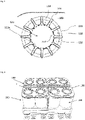
- the pressing member 100 comprises a plate-shaped portion 102 and several leaf springs 110.
- Each leaf spring 110 has a first end 111 which is integral with the plate-shaped portion 102.
- a second end 112 of the leaf spring 110 is distal to the first end 111 and is intended to bear against a body 150 on which the pressing member 100 exerts a force.
- the plate-shaped portion 102 comprises a first through-opening 121 whose edges are entirely formed by the leaf springs 110.
- the leaf springs 110 are juxtaposed one beside the other all along the edge of the opening 121.
- the spring blades 16 are connected by a straight portion of the edge of the opening 14.
- Two spring blades 16 are at a distance from one another.
- the edges of the through opening 121 are completely defined by the leaf springs 110.
- the through opening 121 comprises more leaf springs compared to the prior art. This makes it possible to reduce the individual force exerted by a leaf spring and thus to preserve the surface of the body 150 pressed by the pressing member 100.
- the leaf springs 110 are defined by a succession of convex arcs 113 and concave arcs 114. These arcs 113, 114 are for example defined in the portion 102 in the form of a plate. In particular, all of the second ends 112 of the leaf springs 110 define a central free zone 121a around which they are evenly distributed. For example, the portion 102 in the form of a plate undergoes a cut by which material is removed to define the central part 121a of the opening 121, the spring blades 11 being formed all around this central zone 121a by the definition of the arcs convex 113 and concave 114.
- the central free zone 121a makes it possible in particular to leave a portion of the face of the body 150 free of any support, as will be explained later.
- the leaf springs 110 extend radially from the central free zone 121a from their second end 112 towards their first end 111. Once mounted on the body 150, the second ends 112 bear all around the central free zone 121a, thus allowing a support at most of the central free zone 121a.
- first through openings 121 can be regularly distributed in the plate-shaped portion 102, in particular to allow support around several central free zones 121a.
- the pressing member 100 comprises a second through opening 122, the edges of which comprise spring blades 116.
- These spring blades 116 can be staggered, so that in a top view, for example as in figure 2 , the second opening 122 forms in the plate-shaped portion 102 an alternately concave and convex loop in one direction.
- This second opening 122 completes the pressing force exerted by the leaf springs 110 of the first openings 121.
- the second through opening 122 is located between the first openings. 121, in order to allow a plating between the first openings 121.
- the first openings 121 can be distributed over the vertices of a quadrilateral.
- the second opening 122 is then for example located in a middle zone of said quadrilateral. This configuration can be particularly advantageous when the pressing member 100 presses an electrical device 150 as illustrated in figure 4 to 6 , which will be described later.
- the pressing member 100 may further comprise leaf springs 118 located on the periphery of the portion 102 in the form of a plate. These leaf springs 118 are for example located on one edge of the portion 102 in the form of a plate. In particular, the leaf springs 118 extend from the plate-shaped portion 102 away from each other along one direction. These blades 118 located on the periphery also contribute to the force exerted by the pressing member on the body 150.
- leaf springs 110, 116, 118 are distributed over the portion 102 in the form of a plate in order to leave areas of the body 150 free of any support and to multiply the areas of support on the body 150.
- the plating member 100 is obtained from a cut plate. Thanks to its higher number of leaf springs than in the prior art, the pressing member 100 can be formed in a plate having a smaller thickness.
- the thickness of the plate is between 0.4 and 0.5 mm whereas in the prior art the thickness of the plate is between 0.8 and 1 mm.
- the thickness of the plate from which the plating member 100 is obtained can be divided by 2.
- the figure 4 illustrates an assembly 200 according to an example of the invention.
- the assembly 200 comprises an electrical device 150 for example as illustrated in figure 5 .
- the electrical device 150 includes electronic components 152.154. Electrical conductors 160p, 160n are attached to the electronic components 152,154 to connect them electrically.
- the electronic components 152,154 and the electrical conductors 160p, 160n are connected to each other at the level of zones Zf, called fixing zones, visible in figure 6 Where 7 .
- These attachment zones Zf may have a variable height from one zone to another. This is particularly the case when the conductors 160p, 160n are soldered to terminals of the electronic components 152,154.
- the thickness of the welds at the attachment zones Zf may vary from one attachment zone Zf to another.
- These attachment zones Zf can also form protrusions relative to the rest of the portion 102 in the form of a plate.
- the pressing member 100 is positioned on a face F, called the pressing face, of the electrical device 150. By pressing on this pressing face F, the pressing member 100 is configured to press the electrical device 150 against a surface.
- This plating face comprises in particular said attachment zones Zf.
- the pressing member does not take into account the variability of the height of the attachment zones Zf. In doing so, the prior art pressing member can exert a greater force on an attachment zone Zf that is higher than the others. That leads to differentiated wear between the fixing zones.
- each attachment zone Zf comes into a first opening 121 of the pressing member 100.
- the pressing member 100 does not exert any force directly on the attachment zone Zf, and thereby avoids differentiated wear of these attachment zones Zf.
- attachment zones Zf form protrusions relative to the rest of the portion 102 in the form of a plate, this makes it possible to avoid excessive force on these attachment zones Zf relative to the rest of the portion 102 in the form of of plate.
- the second ends 122 of the leaf springs 110 come all around the attachment zone Zf, in particular to evenly distribute the pressing force around the respective attachment zone Zf.
- Each electronic component 152, 154 can comprise two terminals 152p, 154n of the same polarity in the same plane, as for example illustrated in figure 6 .
- the terminals 152p, 154n of an electronic component 152, 154 are at a distance from each other.
- the two corresponding attachment zones Zf are at a distance from each other, for example as illustrated in the figures.
- the pressing member 100 comprises two first openings 121 at a distance from each other which each surround a respective attachment zone Zf.
- the second through-opening 122 is located equidistant between the first openings 121.
- the second opening 122 presses against a middle part of an electronic component 152, 154 so as to improve the pressing of the electronic component 152, 154.
- the components electronics 152, 154 are in particular arranged in line one beside the other, so that all of the electrical terminals are distributed over two parallel planes which are opposite each other. In the figures, the terminals 154p, 154n located in one of these planes are shown.
- the plating face F can comprise a positive polarity and a negative polarity of the electrical device 150.
- the electronic components 152 on a first side of the row of electronic components are head to tail with respect to the electronic components 154 of a second side of the row.
- the first side of the row comprises terminals of opposite polarity to that of the terminals of the second side of the row of electronic components 152, 154.
- An electrical insulation sheet 170p, 170n is interposed in particular between the plating member 100 and the plating face F in order to isolate the plating member 100 from the electrical device 150.
- a plate of Sufficiently thick insulation is necessary to protect the facing face F from the force exerted by the leaf springs.
- the spring blades 110, 116 each exert a lower force compared to the prior art, which makes it possible to use an electrical insulation sheet instead of a plaque.
- Such a sheet is flexible while the insulation plate is rigid.
- the electrical insulation sheet has a thickness of 0.5 mm and is in particular made of polyurethane.
- the electrical insulation plate has a thickness of 2 mm and is in particular made of an epoxy resin composite.
- the assembly 200 comprises an electrical insulation sheet, in particular when a single plating member 100' is used to plate the electrical device 150.
- the plating member is for example such as that illustrated in figure 8 .
- the pressing member 100' is otherwise similar to the pressing member 100 illustrated in the other figures and is used in the same way. way. However, one or more sheets of electrical insulation 170p, 170n can be used in the event that two plating members 100 are used to plate the electrical device 150, for example as illustrated in figure 4 .
- a first part of the plating face F comprises the positive terminals 152p of first electronic components 152 and a second part of the plating face F comprises negative terminals 154n of second electronic components 154.
- the first part of the plating face F is therefore located in the first side of the row of electronic components, and the second part of the plating plate F is located in the second side of the row of electronic components.
- One of the conductors called positive conductor 160p, is connected to the positive terminals 152p of the first electronic components 152.
- a second electrical conductor, called negative conductor 160n is connected to the negative terminals 154n of the second electronic components 154.
- Each electrical conductor 160p, 160n comprises an arm which extends between the first electronic components 152 on the one hand and the second electronic components 154 on the other hand. facing.
- the positive conductor arm 160p connects to the positive terminals of the second electronic components 154.
- the negative conductor arm 160n connects to the negative terminals of the first electronic components 152.
- a first sheet of electrical insulation 170p can be sandwiched between the plating member 100 and the first part of the plating face F and a second sheet of electrical insulation 170n can be interposed between the plating member 100 and the second part of the plating face F.
- the first sheet of electrical insulation 170p can then extend along the arm of the negative conductor 160n and the second sheet of electrical insulation 170n can then extend along the arm of the positive conductor 160p.
- These electrical insulation sheets 170p, 170n contribute to the electrical insulation of the electrical conductors 170p, 170n at the place where these conductors 160p, 160n are closest, that is to say between the first 152 and the second 154 electronic components.
- the first electrical insulation sheet 170p provides electrical insulation between the portion of the positive conductor 160p included in the plating face F and the arm of the negative conductor 160n.
- the second sheet of electrical insulation 170n provides electrical insulation between the portion of the negative conductor 160n included in the plating face F and the arm of the positive conductor 160p.
- the electrical insulation sheets 170n, 170p are therefore integrated into the electronic device 150. To ensure electrical insulation in the plating members 100 and the electrical device 150, these sheets 170n, 170p are therefore used, which are already provided to insulate the conductors 160p, 160n between them. Thus, the integration of the assembly 200 is improved.
- the assembly 200 comprises two plating members 100.
- an electrical insulation sheet is interposed between the plating members 100 and the plating face F; in the example shown in figure 7 , the pressing members 100 come directly against the pressing face F of the electrical device 150.
- Each pressing member 100 is in contact with a respective polarity of the pressing face F.
- the pressing members 100 are insulated electrically from each other, for example by a distance separating them. Such electrical insulation could be obtained by an insulating material interposed between them.
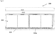
- the figure 9 represents electrical equipment 300 comprising an assembly 200 according to an example of the invention.
- the assembly 200 is mounted on a frame 310 of the electrical equipment 300.
- the pressing member 100 is held in compression between a surface 310a of said frame 310 and the electrical device 150 so as to press the electrical device 150 against a circuit cooling circuit 312 of the electrical equipment 300.
- This cooling circuit 312 comprises in particular a channel 313 through which circulates a fluid intended to drain the heat from the electrical device 150.
- the cooling circuit 312 comes in particular against a face of the electrical device 150, said face being opposite the facing face F.
- the electrical equipment 300 is for example an on-board inverter in a vehicle and configured to supply a motor of the vehicle from a battery.
- the electrical equipment 200 may be a DC-DC voltage converter configured to exchange energy between a high voltage battery and a low voltage battery of the vehicle, or an electrical charger configured to charge a high voltage battery of the vehicle from an electrical network external to the vehicle
- the electrical device is in particular a capacitive block 150 in which the electronic components are capacitors 152, 154.
- the electrical device 150 illustrated could comprise other electronic components, for example in others resistors, or coils inductive.
- the illustrated example comprises several electronic components 152, 154 and two electrical conductors 160p, 160n fixed on the plating face F.
- this example could comprise a single electronic component 152, 154 and a single electrical conductor 160p, 160n fixed on the tackle face F.
Landscapes
- Engineering & Computer Science (AREA)
- Microelectronics & Electronic Packaging (AREA)
- Physics & Mathematics (AREA)
- Thermal Sciences (AREA)
- Structures For Mounting Electric Components On Printed Circuit Boards (AREA)
- Electroplating Methods And Accessories (AREA)
- Connection Of Batteries Or Terminals (AREA)
- Springs (AREA)
Claims (14)
- Presselement (100, 100') zum Pressen einer elektrischen Vorrichtung (150) gegen eine Oberfläche, wobei das Presselement (100, 100') einen plattenförmigen Abschnitt (102) und eine Vielzahl von Federblättern (110) beinhaltet, wobei jedes Federblatt (110) ein erstes Ende (111), das mit dem plattenförmigen Abschnitt (102) einstückig ausgebildet ist, und ein zweites Ende (112), das in Bezug auf das erste Ende (111) distal angeordnet ist, aufweist, wobei das zweite Ende (112) dazu bestimmt ist, an der elektrischen Vorrichtung (150), auf die das Presselement (100, 100') eine Kraft ausübt, zur Anlage zu kommen, wobei der plattenförmige Abschnitt (102) mindestens eine erste Durchgangsöffnung (121) beinhaltet, wobei das Presselement (100, 100') dadurch gekennzeichnet ist, dass die Ränder der ersten Durchgangsöffnung (121) vollständig durch die Vielzahl von Federblättern (110) gebildet sind.
- Presselement (100, 100') nach Anspruch 1, wobei die Federblätter (110) aus einer Folge von konkaven (114) und konvexen (113) Bögen gebildet sind, die insbesondere in dem plattenförmigen Abschnitt (102) definiert sind.
- Presselement (100, 100') nach Anspruch 1 oder 2, wobei die zweiten Enden (112) der Federblätter (110) einen mittigen freien Bereich (121a) definieren, um den herum sie regelmäßig verteilt sind.
- Presselement (100, 100') nach einem der vorhergehenden Ansprüche, das eine Vielzahl der ersten Durchgangsöffnung (121) beinhaltet, deren Ränder jeweils vollständig durch eine Vielzahl von Federblättern (110) gebildet sind.
- Presselement (100, 100') nach einem der vorhergehenden Ansprüche, das mindestens eine zweite Durchgangsöffnung (122) beinhaltet, deren Ränder Federblätter (116) beinhalten.
- Presselement (100, 100') nach den Ansprüchen 4 und 5, wobei sich die mindestens eine zweite Durchgangsöffnung (122) in dem plattenförmigen Abschnitt (102) zwischen den ersten Öffnungen (121) befindet.
- Presselement (100, 100') nach dem vorhergehenden Anspruch, wobei die ersten Öffnungen (121) so angeordnet sind, dass sie sich in den Spitzen eines Vierecks befinden, wobei sich die mindestens eine zweite Öffnung (122) in einem mittleren Bereich des Vierecks befindet.
- Anordnung (200), die eine elektrische Vorrichtung (150) und mindestens ein Presselement (100, 100') nach einem der vorhergehenden Ansprüche beinhaltet, wobei in der Anordnung (200):- die elektrische Vorrichtung (150) mindestens eine elektronische Komponente (152, 154) und mindestens einen elektrischen Leiter (160p, 160n), der an der elektronischen Komponente (152, 154) befestigt ist, um diese elektrisch zu verbinden, beinhaltet, wobei die elektronische Komponente (152, 154) und der elektrische Leiter (160p, 160n) in einem Bereich, der als Befestigungsbereich bezeichnet wird, miteinander verbunden sind,- das Presselement (100, 100') dazu konfiguriert ist, die elektrische Vorrichtung (150) gegen eine Oberfläche zu pressen, indem es gegen eine Fläche (F), die als Pressfläche bezeichnet wird, der elektrischen Vorrichtung (150) drückt, die den Befestigungsbereich beinhaltet,wobei der Befestigungsbereich beim Pressen der elektrischen Vorrichtung (150) durch das Presselement (100, 100') in der ersten Öffnung des Presselements (100, 100') zu liegen kommt.
- Anordnung (200) nach Anspruch 8, die ein Presselement (100, 100') nach den Ansprüchen 4 und 6 beinhaltet, und wobei:- die Pressfläche (F) zwei voneinander beabstandete Befestigungsbereiche beinhaltet,- das Presselement (100, 100') zwei voneinander beabstandete erste Öffnungen beinhaltet, sodass sie jeweils einen Befestigungsbereich umgeben, wobei sich die zweite Durchgangsöffnung gleich weit entfernt zwischen den ersten Öffnungen befindet.
- Anordnung (200) nach Anspruch 8 oder 9, wobei die Pressfläche (F) der elektrischen Vorrichtung (150) eine positive Polarität und eine negative Polarität der elektrischen Vorrichtung (150) beinhaltet.
- Anordnung (200) nach einem der Ansprüche 9 bis 10, wobei mindestens eine elektrische Isolationsfolie zwischen das Presselement (100') und die Pressfläche (F) eingefügt ist.
- Anordnung (200) nach den Ansprüchen 10 und 11, wobei die elektrische Vorrichtung (150) Folgendes umfasst:- mindestens zwei elektronische Komponenten (152, 154), sodass ein erster Teil der Pressfläche (F) eine positive Klemme (152p) einer ersten elektronischen Komponente (152) beinhaltet und ein zweiter Teil der Pressfläche (F) eine negative Klemme (154n) einer zweiten elektronischen Komponente (154) beinhaltet,- einen ersten elektrischen Leiter (160p), der mit der positiven Klemme (152p) der ersten elektronischen Komponente (152) verbunden ist, und einen zweiten elektrischen Leiter (160n), der mit der negativen Klemme (154n) der zweiten elektronischen Komponente (154) verbunden ist, wobei der erste (160p) und der zweite (160n) elektrische Leiter jeweils einen Arm umfassen, der sich zwischen der ersten (152) und der zweiten (154) elektronischen Komponente erstreckt, um sich mit einer positiven Klemme der zweiten elektronischen Komponenten (154) bzw. mit einer negativen Klemme der ersten elektronischen Komponente (152) zu verbinden, wobei die Arme nebeneinander angeordnet sind,wobei die Anordnung (200) eine erste elektrische Isolationsfolie (170p), die zwischen das Presselement (100, 100') und den ersten Teil der Pressfläche (F) eingefügt ist, und eine zweite elektrische Isolationsfolie (170n), die zwischen das Presselement (100, 100') und den zweiten Teil der Pressfläche (F) eingefügt ist, beinhaltet, wobei sich die erste (170p) und die zweite (170n) elektrische Isolationsfolie entlang des Arms (20) des zweiten elektrischen Leiters (160n) bzw. des Arms des ersten elektrischen Leiters (160p) erstrecken, um die elektrischen Leiter (160p, 160n) elektrisch voneinander zu isolieren.
- Anordnung (200) nach Anspruch 10, die zwei Presselemente (100) nach einem der Ansprüche 1 bis 7 beinhaltet, wobei jedes Presselement (100) direkt mit einer jeweiligen Polarität in Kontakt ist, wobei die Presselemente (100) elektrisch voneinander isoliert sind.
- Elektrische Ausrüstung (300), die ein Gestell (310) und eine Anordnung (200) nach einem der Ansprüche 8 bis 13 beinhaltet, wobei das Presselement (100, 100') zwischen einer Oberfläche (310a) des Gestells (310) und der elektrischen Vorrichtung (150) eingeklemmt ist, um die elektrische Vorrichtung (150) gegen einen Kühlkreis (312) der elektrischen Ausrüstung zu pressen.
Applications Claiming Priority (1)
| Application Number | Priority Date | Filing Date | Title |
|---|---|---|---|
| FR1873801A FR3091013B1 (fr) | 2018-12-21 | 2018-12-21 | Organe de plaquage, ensemble et équipement électrique |
Publications (2)
| Publication Number | Publication Date |
|---|---|
| EP3672382A1 EP3672382A1 (de) | 2020-06-24 |
| EP3672382B1 true EP3672382B1 (de) | 2022-08-03 |
Family
ID=66641086
Family Applications (1)
| Application Number | Title | Priority Date | Filing Date |
|---|---|---|---|
| EP19213473.2A Active EP3672382B1 (de) | 2018-12-21 | 2019-12-04 | Presselement, montage und elektrische ausrüstung |
Country Status (3)
| Country | Link |
|---|---|
| EP (1) | EP3672382B1 (de) |
| CN (1) | CN111356334A (de) |
| FR (1) | FR3091013B1 (de) |
Family Cites Families (7)
| Publication number | Priority date | Publication date | Assignee | Title |
|---|---|---|---|---|
| JP3330893B2 (ja) * | 1999-02-04 | 2002-09-30 | シャープ株式会社 | 金属筐体に囲まれた電子部品の放熱構造 |
| DE10142987A1 (de) * | 2001-09-01 | 2003-04-03 | Conti Temic Microelectronic | Wärmeableitelement für elektronische Bauteile |
| JP2005116650A (ja) * | 2003-10-06 | 2005-04-28 | Sanyo Electric Co Ltd | 回路装置 |
| FR2995138B1 (fr) | 2012-08-29 | 2018-02-23 | Valeo Systemes De Controle Moteur | Organe de plaquage d'une piece sur une surface |
| DE102013104949B3 (de) * | 2013-05-14 | 2014-04-24 | Semikron Elektronik Gmbh & Co. Kg | Leistungselektronische Schalteinrichtung und Anordnung hiermit |
| US9564697B2 (en) * | 2014-11-13 | 2017-02-07 | Lear Corporation | Press fit electrical terminal having a solder tab shorter than PCB thickness and method of using same |
| FR3046904B1 (fr) * | 2016-01-20 | 2018-03-02 | Valeo Systemes De Controle Moteur | Equipement electrique, notamment pour vehicule automobile |
-
2018
- 2018-12-21 FR FR1873801A patent/FR3091013B1/fr active Active
-
2019
- 2019-12-04 EP EP19213473.2A patent/EP3672382B1/de active Active
- 2019-12-17 CN CN201911301236.8A patent/CN111356334A/zh active Pending
Also Published As
| Publication number | Publication date |
|---|---|
| EP3672382A1 (de) | 2020-06-24 |
| FR3091013A1 (fr) | 2020-06-26 |
| FR3091013B1 (fr) | 2021-01-15 |
| CN111356334A (zh) | 2020-06-30 |
Similar Documents
| Publication | Publication Date | Title |
|---|---|---|
| EP1886401B1 (de) | Elektronikmodul für eine elektrische drehmaschine | |
| EP3871296B1 (de) | Verbindungsvorrichtung für ein mit einem temperatursensor ausgestattetes fahrzeug | |
| EP1908136B1 (de) | Elektrisches auschlussterminals für eine elektrische stromspeicherzelle | |
| FR2886476A1 (fr) | Piece d'interconnexion de puissance pour machine electrique tournante | |
| WO2006129030A1 (fr) | Piece d'interconnexion de signal pour machine electrique tournante | |
| EP2286492B1 (de) | Bürstenhaltereinrichtung und verwendung dafür zur herstellung eines kraftfahrzeuganlassers | |
| EP1269604B1 (de) | Elektrischer verbinder mit mehrfachkontaktelementen und drehende elektrische maschine mit einem solchen verbinder | |
| EP2891178B1 (de) | Körper zum pressen eines teils auf eine oberfläche | |
| EP3840557A1 (de) | Elektrisches gerät mit einer elektrischen anschlussleiste, die von zwei seiten eines kühlkörpers gekühlt wird | |
| FR3097095A1 (fr) | Équipement electrique comprenant un élément élastique de fixation | |
| EP3614817B1 (de) | Elektrische einheit | |
| EP3672382B1 (de) | Presselement, montage und elektrische ausrüstung | |
| EP2536261B1 (de) | Elektronisches Leistungsmodul mit integrierter Kapazität | |
| EP2745661B1 (de) | Elektrische verbindungsvorrichtung, anordnung mit einer solchen vorrichtung und elektronikplatine sowie verfahren zum elektrischen anschluss einer elektronikplatine | |
| FR2959609A1 (fr) | Ensemble accumulateur pour batterie de vehicule electrique ou hybride | |
| EP1933425B1 (de) | Gesicherter elektrischer Kontakt | |
| EP2438651A1 (de) | Einrichtung zum verbinden eines elektrischen verbinders und eines abgeschirmten elektrischen koaxialkabels und entsprechender elektrischer verbinder | |
| FR3060901B1 (fr) | Module electronique de puissance | |
| WO2024121480A1 (fr) | Guide de connecteurs pour onduleur comportant un organe de plaquage | |
| EP3672383B1 (de) | Einheit, die eine elektrische vorrichtung, ein plattierorgan und ein halteelement des plattierorgans umfasst | |
| FR3076063A1 (fr) | Barre de fixation monobloc electriquement isolante pour equipement electrique de vehicule | |
| EP1371113B1 (de) | Stromverbinder für eine gedruckte schaltung | |
| FR2928784A1 (fr) | Dispositif de raccordement electrique notamment pour panneau solaire electrique | |
| EP3109943A1 (de) | Elektrische verbindungsvorrichtung für eine elektrogerät | |
| FR2836773A1 (fr) | Dispositif de connexion d'un conducteur electrique a une carte a circuit imprime |
Legal Events
| Date | Code | Title | Description |
|---|---|---|---|
| PUAI | Public reference made under article 153(3) epc to a published international application that has entered the european phase |
Free format text: ORIGINAL CODE: 0009012 |
|
| STAA | Information on the status of an ep patent application or granted ep patent |
Free format text: STATUS: THE APPLICATION HAS BEEN PUBLISHED |
|
| AK | Designated contracting states |
Kind code of ref document: A1 Designated state(s): AL AT BE BG CH CY CZ DE DK EE ES FI FR GB GR HR HU IE IS IT LI LT LU LV MC MK MT NL NO PL PT RO RS SE SI SK SM TR |
|
| AX | Request for extension of the european patent |
Extension state: BA ME |
|
| STAA | Information on the status of an ep patent application or granted ep patent |
Free format text: STATUS: REQUEST FOR EXAMINATION WAS MADE |
|
| 17P | Request for examination filed |
Effective date: 20201216 |
|
| RBV | Designated contracting states (corrected) |
Designated state(s): AL AT BE BG CH CY CZ DE DK EE ES FI FR GB GR HR HU IE IS IT LI LT LU LV MC MK MT NL NO PL PT RO RS SE SI SK SM TR |
|
| GRAP | Despatch of communication of intention to grant a patent |
Free format text: ORIGINAL CODE: EPIDOSNIGR1 |
|
| STAA | Information on the status of an ep patent application or granted ep patent |
Free format text: STATUS: GRANT OF PATENT IS INTENDED |
|
| INTG | Intention to grant announced |
Effective date: 20220225 |
|
| GRAS | Grant fee paid |
Free format text: ORIGINAL CODE: EPIDOSNIGR3 |
|
| GRAA | (expected) grant |
Free format text: ORIGINAL CODE: 0009210 |
|
| STAA | Information on the status of an ep patent application or granted ep patent |
Free format text: STATUS: THE PATENT HAS BEEN GRANTED |
|
| AK | Designated contracting states |
Kind code of ref document: B1 Designated state(s): AL AT BE BG CH CY CZ DE DK EE ES FI FR GB GR HR HU IE IS IT LI LT LU LV MC MK MT NL NO PL PT RO RS SE SI SK SM TR |
|
| RIN1 | Information on inventor provided before grant (corrected) |
Inventor name: POUILLY, AURELIEN Inventor name: LEGENDRE, ALEXANDRE |
|
| REG | Reference to a national code |
Ref country code: AT Ref legal event code: REF Ref document number: 1509804 Country of ref document: AT Kind code of ref document: T Effective date: 20220815 Ref country code: CH Ref legal event code: EP |
|
| REG | Reference to a national code |
Ref country code: DE Ref legal event code: R096 Ref document number: 602019017730 Country of ref document: DE |
|
| REG | Reference to a national code |
Ref country code: IE Ref legal event code: FG4D Free format text: LANGUAGE OF EP DOCUMENT: FRENCH |
|
| RAP4 | Party data changed (patent owner data changed or rights of a patent transferred) |
Owner name: VALEO EAUTOMOTIVE FRANCE SAS |
|
| REG | Reference to a national code |
Ref country code: LT Ref legal event code: MG9D |
|
| REG | Reference to a national code |
Ref country code: NL Ref legal event code: MP Effective date: 20220803 |
|
| PG25 | Lapsed in a contracting state [announced via postgrant information from national office to epo] |
Ref country code: SE Free format text: LAPSE BECAUSE OF FAILURE TO SUBMIT A TRANSLATION OF THE DESCRIPTION OR TO PAY THE FEE WITHIN THE PRESCRIBED TIME-LIMIT Effective date: 20220803 Ref country code: RS Free format text: LAPSE BECAUSE OF FAILURE TO SUBMIT A TRANSLATION OF THE DESCRIPTION OR TO PAY THE FEE WITHIN THE PRESCRIBED TIME-LIMIT Effective date: 20220803 Ref country code: PT Free format text: LAPSE BECAUSE OF FAILURE TO SUBMIT A TRANSLATION OF THE DESCRIPTION OR TO PAY THE FEE WITHIN THE PRESCRIBED TIME-LIMIT Effective date: 20221205 Ref country code: NO Free format text: LAPSE BECAUSE OF FAILURE TO SUBMIT A TRANSLATION OF THE DESCRIPTION OR TO PAY THE FEE WITHIN THE PRESCRIBED TIME-LIMIT Effective date: 20221103 Ref country code: NL Free format text: LAPSE BECAUSE OF FAILURE TO SUBMIT A TRANSLATION OF THE DESCRIPTION OR TO PAY THE FEE WITHIN THE PRESCRIBED TIME-LIMIT Effective date: 20220803 Ref country code: LV Free format text: LAPSE BECAUSE OF FAILURE TO SUBMIT A TRANSLATION OF THE DESCRIPTION OR TO PAY THE FEE WITHIN THE PRESCRIBED TIME-LIMIT Effective date: 20220803 Ref country code: LT Free format text: LAPSE BECAUSE OF FAILURE TO SUBMIT A TRANSLATION OF THE DESCRIPTION OR TO PAY THE FEE WITHIN THE PRESCRIBED TIME-LIMIT Effective date: 20220803 Ref country code: FI Free format text: LAPSE BECAUSE OF FAILURE TO SUBMIT A TRANSLATION OF THE DESCRIPTION OR TO PAY THE FEE WITHIN THE PRESCRIBED TIME-LIMIT Effective date: 20220803 Ref country code: ES Free format text: LAPSE BECAUSE OF FAILURE TO SUBMIT A TRANSLATION OF THE DESCRIPTION OR TO PAY THE FEE WITHIN THE PRESCRIBED TIME-LIMIT Effective date: 20220803 |
|
| REG | Reference to a national code |
Ref country code: AT Ref legal event code: MK05 Ref document number: 1509804 Country of ref document: AT Kind code of ref document: T Effective date: 20220803 |
|
| PG25 | Lapsed in a contracting state [announced via postgrant information from national office to epo] |
Ref country code: PL Free format text: LAPSE BECAUSE OF FAILURE TO SUBMIT A TRANSLATION OF THE DESCRIPTION OR TO PAY THE FEE WITHIN THE PRESCRIBED TIME-LIMIT Effective date: 20220803 Ref country code: IS Free format text: LAPSE BECAUSE OF FAILURE TO SUBMIT A TRANSLATION OF THE DESCRIPTION OR TO PAY THE FEE WITHIN THE PRESCRIBED TIME-LIMIT Effective date: 20221203 Ref country code: HR Free format text: LAPSE BECAUSE OF FAILURE TO SUBMIT A TRANSLATION OF THE DESCRIPTION OR TO PAY THE FEE WITHIN THE PRESCRIBED TIME-LIMIT Effective date: 20220803 Ref country code: GR Free format text: LAPSE BECAUSE OF FAILURE TO SUBMIT A TRANSLATION OF THE DESCRIPTION OR TO PAY THE FEE WITHIN THE PRESCRIBED TIME-LIMIT Effective date: 20221104 |
|
| PG25 | Lapsed in a contracting state [announced via postgrant information from national office to epo] |
Ref country code: SM Free format text: LAPSE BECAUSE OF FAILURE TO SUBMIT A TRANSLATION OF THE DESCRIPTION OR TO PAY THE FEE WITHIN THE PRESCRIBED TIME-LIMIT Effective date: 20220803 Ref country code: RO Free format text: LAPSE BECAUSE OF FAILURE TO SUBMIT A TRANSLATION OF THE DESCRIPTION OR TO PAY THE FEE WITHIN THE PRESCRIBED TIME-LIMIT Effective date: 20220803 Ref country code: DK Free format text: LAPSE BECAUSE OF FAILURE TO SUBMIT A TRANSLATION OF THE DESCRIPTION OR TO PAY THE FEE WITHIN THE PRESCRIBED TIME-LIMIT Effective date: 20220803 Ref country code: CZ Free format text: LAPSE BECAUSE OF FAILURE TO SUBMIT A TRANSLATION OF THE DESCRIPTION OR TO PAY THE FEE WITHIN THE PRESCRIBED TIME-LIMIT Effective date: 20220803 Ref country code: AT Free format text: LAPSE BECAUSE OF FAILURE TO SUBMIT A TRANSLATION OF THE DESCRIPTION OR TO PAY THE FEE WITHIN THE PRESCRIBED TIME-LIMIT Effective date: 20220803 |
|
| REG | Reference to a national code |
Ref country code: DE Ref legal event code: R097 Ref document number: 602019017730 Country of ref document: DE |
|
| PG25 | Lapsed in a contracting state [announced via postgrant information from national office to epo] |
Ref country code: SK Free format text: LAPSE BECAUSE OF FAILURE TO SUBMIT A TRANSLATION OF THE DESCRIPTION OR TO PAY THE FEE WITHIN THE PRESCRIBED TIME-LIMIT Effective date: 20220803 Ref country code: EE Free format text: LAPSE BECAUSE OF FAILURE TO SUBMIT A TRANSLATION OF THE DESCRIPTION OR TO PAY THE FEE WITHIN THE PRESCRIBED TIME-LIMIT Effective date: 20220803 |
|
| PLBE | No opposition filed within time limit |
Free format text: ORIGINAL CODE: 0009261 |
|
| STAA | Information on the status of an ep patent application or granted ep patent |
Free format text: STATUS: NO OPPOSITION FILED WITHIN TIME LIMIT |
|
| PG25 | Lapsed in a contracting state [announced via postgrant information from national office to epo] |
Ref country code: AL Free format text: LAPSE BECAUSE OF FAILURE TO SUBMIT A TRANSLATION OF THE DESCRIPTION OR TO PAY THE FEE WITHIN THE PRESCRIBED TIME-LIMIT Effective date: 20220803 |
|
| 26N | No opposition filed |
Effective date: 20230504 |
|
| REG | Reference to a national code |
Ref country code: CH Ref legal event code: PL |
|
| P01 | Opt-out of the competence of the unified patent court (upc) registered |
Effective date: 20230629 |
|
| REG | Reference to a national code |
Ref country code: BE Ref legal event code: MM Effective date: 20221231 |
|
| PG25 | Lapsed in a contracting state [announced via postgrant information from national office to epo] |
Ref country code: SI Free format text: LAPSE BECAUSE OF FAILURE TO SUBMIT A TRANSLATION OF THE DESCRIPTION OR TO PAY THE FEE WITHIN THE PRESCRIBED TIME-LIMIT Effective date: 20220803 Ref country code: LU Free format text: LAPSE BECAUSE OF NON-PAYMENT OF DUE FEES Effective date: 20221204 |
|
| PG25 | Lapsed in a contracting state [announced via postgrant information from national office to epo] |
Ref country code: LI Free format text: LAPSE BECAUSE OF NON-PAYMENT OF DUE FEES Effective date: 20221231 Ref country code: IE Free format text: LAPSE BECAUSE OF NON-PAYMENT OF DUE FEES Effective date: 20221204 Ref country code: CH Free format text: LAPSE BECAUSE OF NON-PAYMENT OF DUE FEES Effective date: 20221231 |
|
| PG25 | Lapsed in a contracting state [announced via postgrant information from national office to epo] |
Ref country code: BE Free format text: LAPSE BECAUSE OF NON-PAYMENT OF DUE FEES Effective date: 20221231 |
|
| PG25 | Lapsed in a contracting state [announced via postgrant information from national office to epo] |
Ref country code: HU Free format text: LAPSE BECAUSE OF FAILURE TO SUBMIT A TRANSLATION OF THE DESCRIPTION OR TO PAY THE FEE WITHIN THE PRESCRIBED TIME-LIMIT; INVALID AB INITIO Effective date: 20191204 |
|
| PG25 | Lapsed in a contracting state [announced via postgrant information from national office to epo] |
Ref country code: CY Free format text: LAPSE BECAUSE OF FAILURE TO SUBMIT A TRANSLATION OF THE DESCRIPTION OR TO PAY THE FEE WITHIN THE PRESCRIBED TIME-LIMIT Effective date: 20220803 |
|
| PG25 | Lapsed in a contracting state [announced via postgrant information from national office to epo] |
Ref country code: MK Free format text: LAPSE BECAUSE OF FAILURE TO SUBMIT A TRANSLATION OF THE DESCRIPTION OR TO PAY THE FEE WITHIN THE PRESCRIBED TIME-LIMIT Effective date: 20220803 Ref country code: IT Free format text: LAPSE BECAUSE OF FAILURE TO SUBMIT A TRANSLATION OF THE DESCRIPTION OR TO PAY THE FEE WITHIN THE PRESCRIBED TIME-LIMIT Effective date: 20220803 |
|
| PG25 | Lapsed in a contracting state [announced via postgrant information from national office to epo] |
Ref country code: MC Free format text: LAPSE BECAUSE OF FAILURE TO SUBMIT A TRANSLATION OF THE DESCRIPTION OR TO PAY THE FEE WITHIN THE PRESCRIBED TIME-LIMIT Effective date: 20220803 |
|
| PG25 | Lapsed in a contracting state [announced via postgrant information from national office to epo] |
Ref country code: MC Free format text: LAPSE BECAUSE OF FAILURE TO SUBMIT A TRANSLATION OF THE DESCRIPTION OR TO PAY THE FEE WITHIN THE PRESCRIBED TIME-LIMIT Effective date: 20220803 |
|
| PG25 | Lapsed in a contracting state [announced via postgrant information from national office to epo] |
Ref country code: BG Free format text: LAPSE BECAUSE OF FAILURE TO SUBMIT A TRANSLATION OF THE DESCRIPTION OR TO PAY THE FEE WITHIN THE PRESCRIBED TIME-LIMIT Effective date: 20220803 |
|
| PG25 | Lapsed in a contracting state [announced via postgrant information from national office to epo] |
Ref country code: MT Free format text: LAPSE BECAUSE OF FAILURE TO SUBMIT A TRANSLATION OF THE DESCRIPTION OR TO PAY THE FEE WITHIN THE PRESCRIBED TIME-LIMIT Effective date: 20220803 |
|
| PGFP | Annual fee paid to national office [announced via postgrant information from national office to epo] |
Ref country code: DE Payment date: 20241211 Year of fee payment: 6 |
|
| PG25 | Lapsed in a contracting state [announced via postgrant information from national office to epo] |
Ref country code: TR Free format text: LAPSE BECAUSE OF FAILURE TO SUBMIT A TRANSLATION OF THE DESCRIPTION OR TO PAY THE FEE WITHIN THE PRESCRIBED TIME-LIMIT Effective date: 20220803 |
|
| PGFP | Annual fee paid to national office [announced via postgrant information from national office to epo] |
Ref country code: GB Payment date: 20251229 Year of fee payment: 7 |
|
| PGFP | Annual fee paid to national office [announced via postgrant information from national office to epo] |
Ref country code: FR Payment date: 20251230 Year of fee payment: 7 |