EP3672382B1 - Pressing element, assembly and electrical equipment - Google Patents
Pressing element, assembly and electrical equipment Download PDFInfo
- Publication number
- EP3672382B1 EP3672382B1 EP19213473.2A EP19213473A EP3672382B1 EP 3672382 B1 EP3672382 B1 EP 3672382B1 EP 19213473 A EP19213473 A EP 19213473A EP 3672382 B1 EP3672382 B1 EP 3672382B1
- Authority
- EP
- European Patent Office
- Prior art keywords
- pressing member
- electrical
- pressing
- assembly
- electrical device
- Prior art date
- Legal status (The legal status is an assumption and is not a legal conclusion. Google has not performed a legal analysis and makes no representation as to the accuracy of the status listed.)
- Active
Links
- 239000004020 conductor Substances 0.000 claims description 37
- 238000010292 electrical insulation Methods 0.000 claims description 28
- 238000001816 cooling Methods 0.000 claims description 9
- 238000007747 plating Methods 0.000 description 44
- 238000005253 cladding Methods 0.000 description 3
- 238000002955 isolation Methods 0.000 description 3
- 239000003990 capacitor Substances 0.000 description 2
- 230000006835 compression Effects 0.000 description 2
- 238000007906 compression Methods 0.000 description 2
- 238000009413 insulation Methods 0.000 description 2
- 230000015556 catabolic process Effects 0.000 description 1
- 239000002131 composite material Substances 0.000 description 1
- 238000006731 degradation reaction Methods 0.000 description 1
- 230000000694 effects Effects 0.000 description 1
- 239000003822 epoxy resin Substances 0.000 description 1
- 239000012530 fluid Substances 0.000 description 1
- 230000001939 inductive effect Effects 0.000 description 1
- 239000011810 insulating material Substances 0.000 description 1
- 230000010354 integration Effects 0.000 description 1
- 239000000463 material Substances 0.000 description 1
- 229920000647 polyepoxide Polymers 0.000 description 1
- 239000004814 polyurethane Substances 0.000 description 1
- 229920002635 polyurethane Polymers 0.000 description 1
- 239000002344 surface layer Substances 0.000 description 1
Images


Classifications
-
- H—ELECTRICITY
- H05—ELECTRIC TECHNIQUES NOT OTHERWISE PROVIDED FOR
- H05K—PRINTED CIRCUITS; CASINGS OR CONSTRUCTIONAL DETAILS OF ELECTRIC APPARATUS; MANUFACTURE OF ASSEMBLAGES OF ELECTRICAL COMPONENTS
- H05K7/00—Constructional details common to different types of electric apparatus
- H05K7/20—Modifications to facilitate cooling, ventilating, or heating
- H05K7/2039—Modifications to facilitate cooling, ventilating, or heating characterised by the heat transfer by conduction from the heat generating element to a dissipating body
- H05K7/20436—Inner thermal coupling elements in heat dissipating housings, e.g. protrusions or depressions integrally formed in the housing
- H05K7/2049—Pressing means used to urge contact, e.g. springs
-
- H—ELECTRICITY
- H05—ELECTRIC TECHNIQUES NOT OTHERWISE PROVIDED FOR
- H05K—PRINTED CIRCUITS; CASINGS OR CONSTRUCTIONAL DETAILS OF ELECTRIC APPARATUS; MANUFACTURE OF ASSEMBLAGES OF ELECTRICAL COMPONENTS
- H05K7/00—Constructional details common to different types of electric apparatus
- H05K7/20—Modifications to facilitate cooling, ventilating, or heating
- H05K7/2089—Modifications to facilitate cooling, ventilating, or heating for power electronics, e.g. for inverters for controlling motor
- H05K7/209—Heat transfer by conduction from internal heat source to heat radiating structure
Definitions
- the present invention relates to a plating member, an assembly comprising such a plating member and an electronic device, and electrical equipment comprising such an assembly, for example embedded in a motor vehicle.
- electrical equipment can be an inverter, a voltage converter or an electrical battery charger.
- the electrical equipment used in particular for the traction of the vehicle, can, during operation of the vehicle, have high voltages, for example between 200V and 800V.
- Such electrical equipment comprises for example an inverter, a voltage converter or an on-board electrical charger.
- the generation of heat by Joule effect in the electronic components of this equipment can then become significant at the risk of damaging the electronic component.
- a cooling system of the electronic components is necessary. It is known to use a pressing member to press the electronic component against a surface of the cooling system to improve its cooling.
- a pressing member 11 is known, illustrated in figure 1 , by patent application publication WO2014033382 .
- the pressing member 11 comes against a power electronic module 30 to press it against a surface of a cooling system for the electrical equipment.
- the pressing member 11 comprises a portion in the form of a plate 12 which has openings 14 from which leaf springs 16 extend. In each opening 14 extends a blade 16 or two blades 16 located vis-à-vis.
- the spring plate typically exerts a force of 100 kg on the electronic component 30 via the spring blades 16.
- Each spring blade 16 must therefore exert a force of 12.5 kg on the component 30
- this force exerted by a blade 16 can damage the surface of the component 30, for example a surface layer of the component 30.
- it is known to introduce a second plate interposed between the electronic component 30 and the spring plate 10 However, this additional plate increases the height of the assembly and complicates its assembly.
- What is therefore sought is a system for plating electronic components that makes it possible to limit damage to the surface of the electronic component in a simple and effective manner.
- the present invention relates to a pressing member comprising a plate-shaped portion and a plurality of leaf springs, each leaf spring having a first end integral with the plate-shaped portion and a second end distal with respect to the first end intended to bear against a body on which the pressing member exerts a force.
- the portion in the form of plate comprises at least a first through opening whose edges are integrally formed by said plurality of leaf springs.
- all the edges of the through-opening comprise a leaf spring, which makes it possible to increase the quantity of leaf springs of the pressing member relative to the pressing member of the prior art.
- the pressing force on the body is better distributed between the spring blades, which makes it possible to avoid damage to the surface of the electronic component.
- the leaf springs are formed by a succession of concave and convex arcs, in particular defined in said plate-shaped portion.
- the second ends of the leaf springs define a central free zone around which they are regularly distributed.
- the pressing member comprises a plurality of said first through opening, the edges of each of which are integrally formed by a plurality of leaf springs.
- the pressing member comprises at least one second through-opening, the edges of which comprise leaf springs.
- said at least one second through-opening is located in the plate-shaped portion between said first openings.
- the first openings are arranged so as to be at the vertices of a quadrilateral, the at least one second opening being located in a middle zone of said quadrilateral.
- said cladding face comprises two attachment zones at a distance from each other and the cladding member comprises two first openings at a distance from each other so as to each surround a zone fixing, a second through opening being located equidistant between said first openings.
- the plating face of said electrical device comprises a positive polarity and a negative polarity of said electrical device.
- At least one electrical insulation sheet is interposed between the plating member and the plating face.
- the assembly comprises two plating members, each plating member being directly in contact with a respective polarity, said plating members being electrically isolated from each other.
- the electrical device is a capacitive block and the electronic components are capacitors.
- the invention further relates to electrical equipment comprising a chassis and an assembly according to the invention, in which said pressing member is held in compression between a surface of said chassis and the electrical device, so as to press the electrical device against a circuit cooling of electrical equipment.
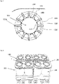
- the pressing member 100 comprises a plate-shaped portion 102 and several leaf springs 110.
- Each leaf spring 110 has a first end 111 which is integral with the plate-shaped portion 102.
- a second end 112 of the leaf spring 110 is distal to the first end 111 and is intended to bear against a body 150 on which the pressing member 100 exerts a force.
- the plate-shaped portion 102 comprises a first through-opening 121 whose edges are entirely formed by the leaf springs 110.
- the leaf springs 110 are juxtaposed one beside the other all along the edge of the opening 121.
- the spring blades 16 are connected by a straight portion of the edge of the opening 14.
- Two spring blades 16 are at a distance from one another.
- the edges of the through opening 121 are completely defined by the leaf springs 110.
- the through opening 121 comprises more leaf springs compared to the prior art. This makes it possible to reduce the individual force exerted by a leaf spring and thus to preserve the surface of the body 150 pressed by the pressing member 100.
- the leaf springs 110 are defined by a succession of convex arcs 113 and concave arcs 114. These arcs 113, 114 are for example defined in the portion 102 in the form of a plate. In particular, all of the second ends 112 of the leaf springs 110 define a central free zone 121a around which they are evenly distributed. For example, the portion 102 in the form of a plate undergoes a cut by which material is removed to define the central part 121a of the opening 121, the spring blades 11 being formed all around this central zone 121a by the definition of the arcs convex 113 and concave 114.
- the central free zone 121a makes it possible in particular to leave a portion of the face of the body 150 free of any support, as will be explained later.
- the leaf springs 110 extend radially from the central free zone 121a from their second end 112 towards their first end 111. Once mounted on the body 150, the second ends 112 bear all around the central free zone 121a, thus allowing a support at most of the central free zone 121a.
- first through openings 121 can be regularly distributed in the plate-shaped portion 102, in particular to allow support around several central free zones 121a.
- the pressing member 100 comprises a second through opening 122, the edges of which comprise spring blades 116.
- These spring blades 116 can be staggered, so that in a top view, for example as in figure 2 , the second opening 122 forms in the plate-shaped portion 102 an alternately concave and convex loop in one direction.
- This second opening 122 completes the pressing force exerted by the leaf springs 110 of the first openings 121.
- the second through opening 122 is located between the first openings. 121, in order to allow a plating between the first openings 121.
- the first openings 121 can be distributed over the vertices of a quadrilateral.
- the second opening 122 is then for example located in a middle zone of said quadrilateral. This configuration can be particularly advantageous when the pressing member 100 presses an electrical device 150 as illustrated in figure 4 to 6 , which will be described later.
- the pressing member 100 may further comprise leaf springs 118 located on the periphery of the portion 102 in the form of a plate. These leaf springs 118 are for example located on one edge of the portion 102 in the form of a plate. In particular, the leaf springs 118 extend from the plate-shaped portion 102 away from each other along one direction. These blades 118 located on the periphery also contribute to the force exerted by the pressing member on the body 150.
- leaf springs 110, 116, 118 are distributed over the portion 102 in the form of a plate in order to leave areas of the body 150 free of any support and to multiply the areas of support on the body 150.
- the plating member 100 is obtained from a cut plate. Thanks to its higher number of leaf springs than in the prior art, the pressing member 100 can be formed in a plate having a smaller thickness.
- the thickness of the plate is between 0.4 and 0.5 mm whereas in the prior art the thickness of the plate is between 0.8 and 1 mm.
- the thickness of the plate from which the plating member 100 is obtained can be divided by 2.
- the figure 4 illustrates an assembly 200 according to an example of the invention.
- the assembly 200 comprises an electrical device 150 for example as illustrated in figure 5 .
- the electrical device 150 includes electronic components 152.154. Electrical conductors 160p, 160n are attached to the electronic components 152,154 to connect them electrically.
- the electronic components 152,154 and the electrical conductors 160p, 160n are connected to each other at the level of zones Zf, called fixing zones, visible in figure 6 Where 7 .
- These attachment zones Zf may have a variable height from one zone to another. This is particularly the case when the conductors 160p, 160n are soldered to terminals of the electronic components 152,154.
- the thickness of the welds at the attachment zones Zf may vary from one attachment zone Zf to another.
- These attachment zones Zf can also form protrusions relative to the rest of the portion 102 in the form of a plate.
- the pressing member 100 is positioned on a face F, called the pressing face, of the electrical device 150. By pressing on this pressing face F, the pressing member 100 is configured to press the electrical device 150 against a surface.
- This plating face comprises in particular said attachment zones Zf.
- the pressing member does not take into account the variability of the height of the attachment zones Zf. In doing so, the prior art pressing member can exert a greater force on an attachment zone Zf that is higher than the others. That leads to differentiated wear between the fixing zones.
- each attachment zone Zf comes into a first opening 121 of the pressing member 100.
- the pressing member 100 does not exert any force directly on the attachment zone Zf, and thereby avoids differentiated wear of these attachment zones Zf.
- attachment zones Zf form protrusions relative to the rest of the portion 102 in the form of a plate, this makes it possible to avoid excessive force on these attachment zones Zf relative to the rest of the portion 102 in the form of of plate.
- the second ends 122 of the leaf springs 110 come all around the attachment zone Zf, in particular to evenly distribute the pressing force around the respective attachment zone Zf.
- Each electronic component 152, 154 can comprise two terminals 152p, 154n of the same polarity in the same plane, as for example illustrated in figure 6 .
- the terminals 152p, 154n of an electronic component 152, 154 are at a distance from each other.
- the two corresponding attachment zones Zf are at a distance from each other, for example as illustrated in the figures.
- the pressing member 100 comprises two first openings 121 at a distance from each other which each surround a respective attachment zone Zf.
- the second through-opening 122 is located equidistant between the first openings 121.
- the second opening 122 presses against a middle part of an electronic component 152, 154 so as to improve the pressing of the electronic component 152, 154.
- the components electronics 152, 154 are in particular arranged in line one beside the other, so that all of the electrical terminals are distributed over two parallel planes which are opposite each other. In the figures, the terminals 154p, 154n located in one of these planes are shown.
- the plating face F can comprise a positive polarity and a negative polarity of the electrical device 150.
- the electronic components 152 on a first side of the row of electronic components are head to tail with respect to the electronic components 154 of a second side of the row.
- the first side of the row comprises terminals of opposite polarity to that of the terminals of the second side of the row of electronic components 152, 154.
- An electrical insulation sheet 170p, 170n is interposed in particular between the plating member 100 and the plating face F in order to isolate the plating member 100 from the electrical device 150.
- a plate of Sufficiently thick insulation is necessary to protect the facing face F from the force exerted by the leaf springs.
- the spring blades 110, 116 each exert a lower force compared to the prior art, which makes it possible to use an electrical insulation sheet instead of a plaque.
- Such a sheet is flexible while the insulation plate is rigid.
- the electrical insulation sheet has a thickness of 0.5 mm and is in particular made of polyurethane.
- the electrical insulation plate has a thickness of 2 mm and is in particular made of an epoxy resin composite.
- the assembly 200 comprises an electrical insulation sheet, in particular when a single plating member 100' is used to plate the electrical device 150.
- the plating member is for example such as that illustrated in figure 8 .
- the pressing member 100' is otherwise similar to the pressing member 100 illustrated in the other figures and is used in the same way. way. However, one or more sheets of electrical insulation 170p, 170n can be used in the event that two plating members 100 are used to plate the electrical device 150, for example as illustrated in figure 4 .
- a first part of the plating face F comprises the positive terminals 152p of first electronic components 152 and a second part of the plating face F comprises negative terminals 154n of second electronic components 154.
- the first part of the plating face F is therefore located in the first side of the row of electronic components, and the second part of the plating plate F is located in the second side of the row of electronic components.
- One of the conductors called positive conductor 160p, is connected to the positive terminals 152p of the first electronic components 152.
- a second electrical conductor, called negative conductor 160n is connected to the negative terminals 154n of the second electronic components 154.
- Each electrical conductor 160p, 160n comprises an arm which extends between the first electronic components 152 on the one hand and the second electronic components 154 on the other hand. facing.
- the positive conductor arm 160p connects to the positive terminals of the second electronic components 154.
- the negative conductor arm 160n connects to the negative terminals of the first electronic components 152.
- a first sheet of electrical insulation 170p can be sandwiched between the plating member 100 and the first part of the plating face F and a second sheet of electrical insulation 170n can be interposed between the plating member 100 and the second part of the plating face F.
- the first sheet of electrical insulation 170p can then extend along the arm of the negative conductor 160n and the second sheet of electrical insulation 170n can then extend along the arm of the positive conductor 160p.
- These electrical insulation sheets 170p, 170n contribute to the electrical insulation of the electrical conductors 170p, 170n at the place where these conductors 160p, 160n are closest, that is to say between the first 152 and the second 154 electronic components.
- the first electrical insulation sheet 170p provides electrical insulation between the portion of the positive conductor 160p included in the plating face F and the arm of the negative conductor 160n.
- the second sheet of electrical insulation 170n provides electrical insulation between the portion of the negative conductor 160n included in the plating face F and the arm of the positive conductor 160p.
- the electrical insulation sheets 170n, 170p are therefore integrated into the electronic device 150. To ensure electrical insulation in the plating members 100 and the electrical device 150, these sheets 170n, 170p are therefore used, which are already provided to insulate the conductors 160p, 160n between them. Thus, the integration of the assembly 200 is improved.
- the assembly 200 comprises two plating members 100.
- an electrical insulation sheet is interposed between the plating members 100 and the plating face F; in the example shown in figure 7 , the pressing members 100 come directly against the pressing face F of the electrical device 150.
- Each pressing member 100 is in contact with a respective polarity of the pressing face F.
- the pressing members 100 are insulated electrically from each other, for example by a distance separating them. Such electrical insulation could be obtained by an insulating material interposed between them.
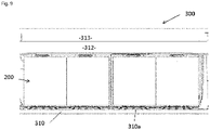
- the figure 9 represents electrical equipment 300 comprising an assembly 200 according to an example of the invention.
- the assembly 200 is mounted on a frame 310 of the electrical equipment 300.
- the pressing member 100 is held in compression between a surface 310a of said frame 310 and the electrical device 150 so as to press the electrical device 150 against a circuit cooling circuit 312 of the electrical equipment 300.
- This cooling circuit 312 comprises in particular a channel 313 through which circulates a fluid intended to drain the heat from the electrical device 150.
- the cooling circuit 312 comes in particular against a face of the electrical device 150, said face being opposite the facing face F.
- the electrical equipment 300 is for example an on-board inverter in a vehicle and configured to supply a motor of the vehicle from a battery.
- the electrical equipment 200 may be a DC-DC voltage converter configured to exchange energy between a high voltage battery and a low voltage battery of the vehicle, or an electrical charger configured to charge a high voltage battery of the vehicle from an electrical network external to the vehicle
- the electrical device is in particular a capacitive block 150 in which the electronic components are capacitors 152, 154.
- the electrical device 150 illustrated could comprise other electronic components, for example in others resistors, or coils inductive.
- the illustrated example comprises several electronic components 152, 154 and two electrical conductors 160p, 160n fixed on the plating face F.
- this example could comprise a single electronic component 152, 154 and a single electrical conductor 160p, 160n fixed on the tackle face F.
Description
La présente invention concerne un organe de plaquage, un ensemble comportant un tel organe de plaquage et un dispositif électronique, et un équipement électrique comprenant un tel ensemble, par exemple embarqué dans un véhicule automobile. Un tel équipement électrique peut être un onduleur, un convertisseur de tension ou un chargeur électrique de batterie.The present invention relates to a plating member, an assembly comprising such a plating member and an electronic device, and electrical equipment comprising such an assembly, for example embedded in a motor vehicle. Such electrical equipment can be an inverter, a voltage converter or an electrical battery charger.
Typiquement, dans des applications de véhicule électrique ou hybride, les équipements électriques, utilisés notamment pour la traction du véhicule, peuvent, au cours du fonctionnement du véhicule, présenter des tensions élevées, par exemple compris entre 200V et 800V. De tels équipements électriques comprennent par exemple un onduleur, un convertisseur de tension ou un chargeur électrique embarqué. La génération de chaleur par effet joule dans les composants électroniques de ces équipements peut alors devenir importante au risque d'endommager le composant électronique. Afin d'éviter toute dégradation par la chaleur, un système de refroidissement des composants électroniques est nécessaire. Il est connu d'utiliser un organe de plaquage pour plaquer le composant électronique contre une surface du système de refroidissement pour améliorer son refroidissement. On connaît un tel organe de plaquage 11, illustré en
Il est donc recherché un système de plaquage des composants électroniques permettant de limiter un dommage de la surface du composant électronique de manière simple et efficace.What is therefore sought is a system for plating electronic components that makes it possible to limit damage to the surface of the electronic component in a simple and effective manner.
À cet effet, la présente invention concerne un organe de plaquage comprenant une portion en forme de plaque et une pluralité de lames ressort, chaque lame ressort ayant une première extrémité intégrale avec la portion en forme de plaque et une deuxième extrémité distale par rapport à la première extrémité destinée à venir en appui contre un corps sur lequel l'organe de plaquage exerce un effort. Dans l'organe de plaquage selon l'invention, la portion en forme de plaque comprend au moins une première ouverture traversante dont les bords sont intégralement formés par ladite pluralité de lames ressort.To this end, the present invention relates to a pressing member comprising a plate-shaped portion and a plurality of leaf springs, each leaf spring having a first end integral with the plate-shaped portion and a second end distal with respect to the first end intended to bear against a body on which the pressing member exerts a force. In the pressing member according to the invention, the portion in the form of plate comprises at least a first through opening whose edges are integrally formed by said plurality of leaf springs.
Ainsi, contrairement à l'art antérieur, tous les bords de l'ouverture traversante comprennent une lame ressort, ce qui permet d'augmenter la quantité de lames ressort de l'organe de plaquage par rapport à l'organe de plaquage de l'art antérieur. Ainsi, l'effort de plaquage sur le corps est mieux réparti entre les lames ressort, ce qui permet d'éviter un endommagement de la surface du composant électronique.Thus, unlike the prior art, all the edges of the through-opening comprise a leaf spring, which makes it possible to increase the quantity of leaf springs of the pressing member relative to the pressing member of the prior art. Thus, the pressing force on the body is better distributed between the spring blades, which makes it possible to avoid damage to the surface of the electronic component.
Selon un mode de réalisation, les lames ressort sont formées par une succession d'arc concaves et convexes, notamment définis dans ladite portion en forme de plaque.According to one embodiment, the leaf springs are formed by a succession of concave and convex arcs, in particular defined in said plate-shaped portion.
Selon un mode de réalisation, les deuxièmes extrémités des lames ressort définissent une zone libre centrale autour de laquelle elles sont régulièrement réparties.According to one embodiment, the second ends of the leaf springs define a central free zone around which they are regularly distributed.
Selon un mode de réalisation, l'organe de plaquage comprend une pluralité de ladite première ouverture traversante, dont les bords de chacune sont intégralement formés par une pluralité de lames ressort.According to one embodiment, the pressing member comprises a plurality of said first through opening, the edges of each of which are integrally formed by a plurality of leaf springs.
Selon un mode de réalisation, l'organe de plaquage comprend au moins une seconde ouverture traversante, dont les bords comprennent des lames ressort.According to one embodiment, the pressing member comprises at least one second through-opening, the edges of which comprise leaf springs.
Selon une variante, ladite au moins une seconde ouverture traversante est située dans la portion en forme de plaque entre lesdites premières ouvertures.According to a variant, said at least one second through-opening is located in the plate-shaped portion between said first openings.
Selon une variante particulière, les premières ouvertures sont agencées de sorte à être aux sommets d'un quadrilatère, l'au moins une deuxième ouverture étant située dans une zone médiane dudit quadrilatère.According to a particular variant, the first openings are arranged so as to be at the vertices of a quadrilateral, the at least one second opening being located in a middle zone of said quadrilateral.
L'invention concerne également un ensemble comprenant un dispositif électrique et au moins un organe de plaquage selon l'invention, ensemble dans lequel :
- ledit dispositif électrique comprend au moins un composant électronique et au moins un conducteur électrique fixé sur ledit composant électronique pour le connecter électriquement, ledit composant électronique et ledit conducteur électrique étant connectés l'un à l'autre au niveau d'une zone, dite zone de fixation,
- l'organe de plaquage est configuré pour plaquer ledit dispositif électrique contre une surface, en venant contre une face, dit face de plaquage, dudit dispositif électrique comprenant ladite zone de fixation ,
- said electrical device comprises at least one electronic component and at least one electrical conductor attached to said electronic component to connect it electrically, said electronic component and said electrical conductor being connected to each other at the level of a zone, called zone of fixation,
- the pressing member is configured to press said electrical device against a surface, coming against a face, called pressing face, of said electrical device comprising said fixing zone,
Selon un mode de réalisation, ladite face de plaquage comprend deux zones de fixation à distance l'une de l'autre et l'organe de plaquage comprend deux premières ouvertures à distance l'une de l'autre de manière à entourer chacune une zone de fixation, une seconde ouverture traversante étant située à équidistance entre lesdites premières ouvertures.According to one embodiment, said cladding face comprises two attachment zones at a distance from each other and the cladding member comprises two first openings at a distance from each other so as to each surround a zone fixing, a second through opening being located equidistant between said first openings.
Selon un mode de réalisation, la face de plaquage dudit dispositif électrique comprend une polarité positive et une polarité négative dudit dispositif électrique.According to one embodiment, the plating face of said electrical device comprises a positive polarity and a negative polarity of said electrical device.
Selon un mode de réalisation, au moins une feuille d'isolation électrique est intercalée entre l'organe de plaquage et la face de plaquage.According to one embodiment, at least one electrical insulation sheet is interposed between the plating member and the plating face.
Selon un mode de réalisation, ledit dispositif électrique comporte :
- au moins deux composants électroniques, tels qu'une première partie de la face de plaquage comprend une borne positive d'un premier composant électronique et une deuxième partie de la face de plaquage comprend une borne négative d'un deuxième composant électronique,
- un premier conducteur électrique, connecté à la borne positive du premier composant électronique et un deuxième conducteur électrique connecté à la borne négative du deuxième composant électronique, le premier et le deuxième conducteur électrique comportant chacun un bras s'étendant entre le premier et le deuxième composant électronique pour se connecter respectivement à une borne positive du deuxième composant électronique et à une borne négative du premier composant électronique, lesdits bras étant agencés l'un à côté de l'autre l'ensemble comprenant une première feuille d'isolation électrique intercalée entre l'organe de plaquage et la première partie de la face de plaquage et une deuxième feuille d'isolation électrique intercalée entre l'organe de plaquage et la deuxième partie de la face de plaquage, la première et la deuxième feuille d'isolation électrique s'étendant respectivement le long du bras du deuxième conducteur électrique et du bras du premier conducteur électrique.de manière à isoler électriquement les conducteurs électriques entre eux.
- at least two electronic components, such that a first part of the plating face comprises a positive terminal of a first electronic component and a second part of the plating face comprises a negative terminal of a second electronic component,
- a first electrical conductor, connected to the positive terminal of the first electronic component and a second electrical conductor connected to the negative terminal of the second electronic component, the first and the second electrical conductor each comprising an arm extending between the first and the second component electronics to connect respectively to a positive terminal of the second electronic component and to a negative terminal of the first electronic component, said arms being arranged one beside the other, the assembly comprising a first sheet of electrical insulation inserted between the 'plating member and the first part of the plating face and a second electrical insulation sheet interposed between the plating member and the second part of the plating face, the first and the second electrical insulation sheet are respectively extending along the arm of the second electrical conductor and the arm of the first electrical conductor. nier to electrically insulate the electrical conductors between them.
Selon un mode de réalisation, l'ensemble comprend deux organes de plaquage, chaque organe de plaquage étant directement en contact avec une polarité respective, lesdits organes de plaquage étant isolés électriquement l'un de l'autre.According to one embodiment, the assembly comprises two plating members, each plating member being directly in contact with a respective polarity, said plating members being electrically isolated from each other.
Selon un mode de réalisation, le dispositif électrique est un bloc capacitif et les composants électroniques sont des condensateurs.According to one embodiment, the electrical device is a capacitive block and the electronic components are capacitors.
L'invention concerne en outre un équipement électrique comprenant un châssis et un ensemble selon l'invention, dans lequel ledit organe de plaquage est pris en compression entre une surface dudit châssis et le dispositif électrique, de manière à plaquer le dispositif électrique contre un circuit de refroidissement de l'équipement électrique.The invention further relates to electrical equipment comprising a chassis and an assembly according to the invention, in which said pressing member is held in compression between a surface of said chassis and the electrical device, so as to press the electrical device against a circuit cooling of electrical equipment.
L'invention sera mieux comprise et d'autres détails, caractéristiques et avantages de l'invention apparaîtront à la lecture de la description suivante faite à titre d'exemple non limitatif en référence aux figures annexées dans lesquelles :
-
Fig. 1 , déjà décrite, présente un organe de plaquage de l'art antérieur ; -
Fig. 2 présente un organe de plaquage selon un exemple de l'invention ; -
Fig. 3 présente une vue agrandie de l'organe de plaquage de lafigure 2 ; -
Fig. 4 présente un ensemble selon un exemple de l'invention ; -
Fig. 5 présente un dispositif électrique d'un ensemble selon un exemple de l'invention ; -
Fig. 6 présente un dispositif électrique d'un ensemble selon un exemple de l'invention ; -
Fig. 7 présente une vue de dessus d'un ensemble selon un exemple de l'invention ; -
Fig. 8 présente un organe de plaquage selon un exemple de l'invention ; -
Fig. 9 présente un équipement électrique selon un exemple de l'invention.
-
Fig. 1 , already described, has a plating member of the prior art; -
Fig. 2 presents a pressing member according to an example of the invention; -
Fig. 3 presents an enlarged view of the plating member of thefigure 2 ; -
Fig. 4 presents an assembly according to an example of the invention; -
Fig. 5 presents an electrical device of an assembly according to an example of the invention; -
Fig. 6 presents an electrical device of an assembly according to an example of the invention; -
Fig. 7 presents a top view of an assembly according to an example of the invention; -
Fig. 8 presents a pressing member according to an example of the invention; -
Fig. 9 presents electrical equipment according to an example of the invention.
Un exemple d'organe de plaquage 100 va être décrit en faisant référence aux
En particulier, les lames ressort 110 sont définies par une succession d'arcs convexes 113 et d'arcs concaves 114. Ces arcs 113, 114 sont par exemple définis dans la portion 102 en forme de plaque. Notamment, l'ensemble des deuxièmes extrémités 112 des lames ressort 110 définissent une zone libre centrale 121a autour de laquelle elles sont régulièrement réparties. Par exemple, la portion 102 en forme de plaque subit une découpe par laquelle on enlève de la matière pour définir la partie centrale 121a de l'ouverture 121, les lames ressort 11 étant formées tout autour de cette zone centrale 121a par la définition des arcs convexes 113 et concaves 114. La zone libre centrale 121a permet notamment de laisser une portion de la face du corps 150 libre de tout appui comme cela sera expliqué plus loin. Les lames ressort 110 s'étendent radialement depuis la zone libre centrale 121a depuis leur deuxième extrémité 112 vers leur première extrémité 111. Une fois montées sur le corps 150, les deuxièmes extrémités 112 appuient tout autour de la zone libre centrale 121a, permettant ainsi un appui au plus de la zone libre centrale 121a.In particular, the
Plusieurs premières ouvertures traversantes 121 peuvent être régulièrement réparties dans la portion en forme de plaque 102, notamment pour permettre un appui autour de plusieurs zones libres centrales 121a.Several first through
Selon une variante, l'organe de plaquage 100 comprend une seconde ouverture traversante 122, dont les bords comprennent des lames ressort 116. Ces lames ressort 116 peuvent être agencées en quinconce, de sorte que dans une vue de dessus, par exemple comme en
Comme illustré sur les figures, les premières ouvertures 121 peuvent être réparties sur les sommets d'un quadrilatère. La seconde ouverture 122 est alors par exemple située dans une zone médiane dudit quadrilatère. Cette configuration peut être particulièrement avantageuse lorsque l'organe de plaquage 100 plaque un dispositif électrique 150 tel qu'illustré en
L'organe de plaquage 100 peut comprendre en outre des lames ressort 118 situées en périphérie de la portion 102 en forme de plaque. Ces lames ressort 118 sont par exemple situées sur un bord de la portion 102 en forme de plaque. Notamment, les lames ressort 118 s'étendent depuis la portion en forme de plaque 102 en s'éloignant l'une de l'autre le long d'une direction. Ces lames 118 situées en périphérie contribuent également à l'effort exercé par l'organe de plaquage sur le corps 150.The pressing
Globalement, l'ensemble des lames ressort 110, 116, 118 sont réparties sur la portion 102 en forme de plaque afin de laisser libre de tout appui des zones du corps 150 et de multiplier les zones d'appui sur le corps 150.Overall, all of the
Par exemple, l'organe de plaquage 100 est obtenu à partir d'une plaque découpée. Grâce à son nombre de lames ressort plus élevé que dans l'art antérieur, l'organe de plaquage 100 peut être formé dans une plaque ayant une épaisseur plus faible. Par exemple, l'épaisseur de la plaque est comprise entre 0,4 et 0,5 mm alors que dans l'art antérieur l'épaisseur de la plaque est comprise entre 0,8 et 1mm. Ainsi, l'épaisseur de la plaque à partir de laquelle l'organe de plaquage 100 est obtenue peut être divisée par 2.For example, the plating
La
L'organe de plaquage 100 est positionné sur une face F, dite face de plaquage, du dispositif électrique 150. En appuyant sur cette face de plaquage F, l'organe de plaquage 100 est configuré pour plaquer le dispositif électrique 150 contre une surface. Cette face de plaquage comprend notamment lesdites zones de fixation Zf.The pressing
Dans une solution de l'art antérieur, l'organe de plaquage ne prend pas en compte la variabilté de la hauteur des zones de fixation Zf. Ce faisant, l'organe de plaquage de l'art antérieur peut exercer un effort plus important sur une zone de fixation Zf plus haute que les autres. Cela entraine une usure différenciée entre les zones de fixation. Dans l'ensemble 200 selon un exemple de l'invention, chaque zone de fixation Zf vient dans une première ouverture 121 de l'organe de plaquage 100. Ainsi, l'organe de plaquage 100 n'exerce pas d'effort directement sur les zone de fixation Zf, et évite de la sorte une usure différenciée de ces zones de fixation Zf. En outre, lorsque ces zones de fixation Zf forment des excroissances par rapport au reste de la portion 102 en forme de plaque, cela permet d'éviter un effort trop important sur ces zones de fixation Zf par rapport au reste de la portion 102 en forme de plaque. Les deuxièmes extrémités 122 des lames ressort 110 viennent tout autour de la zone de fixation Zf, pour notamment répartir régulièrement l'effort de plaquage autour la zone de fixation Zf respective.In a solution of the prior art, the pressing member does not take into account the variability of the height of the attachment zones Zf. In doing so, the prior art pressing member can exert a greater force on an attachment zone Zf that is higher than the others. That leads to differentiated wear between the fixing zones. In the
Chaque composant électronique 152, 154 peut comprendre deux bornes 152p, 154n de même polarité dans un même plan, comme par exemple illustré en
La face de plaquage F peut comprendre une polarité positive et une polarité négative du dispositif électrique 150. Par exemple, les composants électroniques 152 d'un premier côté de la rangée de composants électronique sont tête-bêche par rapport aux composants électroniques 154 d'un deuxième côté de la rangée. Ainsi, vu de la face de plaquage F, le premier côté de la rangée comprend des bornes de polarité opposée à celle des bornes du deuxième côté de la rangée de composants électroniques 152, 154.The plating face F can comprise a positive polarity and a negative polarity of the
Une feuille d'isolation électrique 170p, 170n est notamment intercalée entre l'organe de plaquage 100 et la face de plaquage F afin d'isoler l'organe de plaquage 100 du dispositif électrique 150. Dans l'art antérieur, une plaque d'isolation suffisamment épaisse est nécessaire pour protéger la face de plaquage F de l'effort exercé par les lames ressort. Dans l'ensemble 200 selon l'exemple de l'invention, les lames ressort 110, 116 exercent chacune un effort inférieur par rapport à l'art antérieur, ce qui permet d'utiliser une feuille d'isolation électrique au lieu d'une plaque. Une telle feuille est souple alors que la plaque d'isolation est rigide. Par exemple, la feuille d'isolation électrique a une épaisseur de 0,5mm et est notamment en polyuréthane. Alors que dans l'art antérieur la plaque d'isolation électrique a une épaisseur de 2mm et est notamment en un composite résiné epoxy.An
L'ensemble 200 comprend une feuille d'isolation électrique en particulier lorsqu'un seul organe de plaquage 100' est utilisé pour plaquer le dispositif électrique 150. L'organe de plaquage est par exemple tel que celui illustré en
En particulier, en
Ces feuilles d'isolation électriques 170p, 170n contribuent à l'isolation électrique des conducteurs électriques 170p, 170n à l'endroit où ces conducteurs 160p, 160n sont les plus proches, c'est-à-dire entre les premiers 152 et le deuxièmes 154 composants électroniques. Notamment, la première feuille d'isolation électrique 170p assure une isolation électrique entre la portion du conducteur positif 160p comprise dans la face de plaquage F et le bras du conducteur négatif 160n. De même, la deuxième feuille d'isolation électrique 170n assure une isolation électrique entre la portion du conducteur négatif 160n comprise dans la face de plaquage F et le bras du conducteur positif 160p. Les feuilles d'isolation électriques 170n, 170p sont donc intégrées dans le dispositif électronique 150. Pour assurer l'isolation électrique en les organes de plaquage 100 et le dispositif électrique 150, on utilise donc ces feuilles 170n, 170p qui sont déjà prévues pour isoler les conducteurs 160p, 160n entre eux. Ainsi, l'intégration de l'ensemble 200 est amélioré.These
Dans la variante de l'ensemble 200 illustrée en
La
L'équipement électrique 300 est par exemple un onduleur embarqué dans un véhicule et configuré pour alimenter un moteur du véhicule à partir d'une batterie. Alternativement, l'équipement électrique 200 peut être un convertisseur de tension continu-continu configuré pour échanger de l'énergie entre une batterie haute tension et une batterie basse tension du véhicule, ou un chargeur électrique configuré pour charger une batterie haute tension du véhicule depuis un réseau électrique extérieur au véhiculeThe
Dans les figures, le dispositif électrique est notamment un bloc capacitif 150 dans lequel les composants électroniques sont des condensateurs 152, 154. Cependant, le dispositif électrique 150 illustré pourrait comprendre d'autres composants électroniques, par exemple en autres des résistances, ou des bobines inductives.In the figures, the electrical device is in particular a
L'exemple illustré comprend plusieurs composants électroniques 152, 154 et deux conducteurs électriques 160p, 160n fixés sur la face de plaquage F. Cependant, cet exemple pourrait comprendre un seul composant électronique 152, 154 et un seul conducteur électrique 160p, 160n fixé sur la face de plaquage F.The illustrated example comprises several
Claims (14)
- Pressing member (100, 100') for pressing an electrical device (150) against a surface, the pressing member (100, 100') comprising a portion (102) in the form of a plate and a plurality of spring leaves (110), each spring leaf (110) having a first end (111) integral with the portion (102) in the form of a plate and a second distal end (112) with respect to the first end (111), said second end (112) being intended to bear against the electrical device (150) on which the pressing member (100, 100') exerts a force, said portion (102) in the form of a plate comprising at least one first through-opening (121), the pressing member (100, 100') being characterized in that the edges of the first through-opening (121) are entirely formed by said plurality of spring leaves (110).
- Pressing member (100, 100') according to Claim 1, wherein the spring leaves (110) are formed by a succession of concave (114) and convex (113) arcs, in particular defined in said portion (102) in the form of a plate.
- Pressing member (100, 100') according to Claim 1 or 2, wherein the second ends (112) of the spring leaves (110) define a central free region (121a) about which they are regularly distributed.
- Pressing member (100, 100') according to one of the preceding claims, comprising a plurality of said first through-openings (121), the edges of each of which are entirely formed by a plurality of spring leaves (110).
- Pressing member (100, 100') according to one of the preceding claims, comprising at least one second through-opening (122), the edges of which comprise spring leaves (116).
- Pressing member (100, 100') according to Claims 4 and 5, wherein said at least one second through-opening (122) is situated in the portion (102) in the form of a plate between said first openings (121) .
- Pressing member (100, 100') according to the preceding claim, wherein the first openings (121) are arranged so as to be at the apexes of a quadrilateral, the at least one second opening (122) being situated in a median region of said quadrilateral.
- Assembly (200) comprising an electrical device (150) and at least one pressing member (100, 100') according to one of the preceding claims, in which assembly (200):- said electrical device (150) comprises at least one electronic component (152, 154) and at least one electrical conductor (160p, 160n) fastened to said electronic component (152, 154) in order to connect it electrically, said electronic component (152, 154) and said electrical conductor (160p, 160n) being connected to one another at a region, termed fastening region,- the pressing member (100, 100') is configured to press said electrical device (150) against a surface, coming against a face (F), termed pressing face, of said electrical device (150) comprising said fastening region, said fastening region coming into the first opening of the pressing member (100, 100') during the pressing of said electrical device (150) by the pressing member (100, 100').
- Assembly (200) according to Claim 8, comprising a pressing member (100, 100') according to Claims 4 and 6, and wherein:- said pressing face (F) comprises two fastening regions at a distance from one another,- the pressing member (100, 100') comprises two first openings at a distance from one another so as to each surround a fastening region, the second through-opening being situated equidistantly between said first openings.
- Assembly (200) according to Claim 8 or 9, wherein the pressing face (F) of said electrical device (150) comprises a positive polarity and a negative polarity of said electrical device (150).
- Assembly (200) according to either of Claims 9 and 10, wherein at least one electrical insulation sheet is interposed between the pressing member (100') and the pressing face (F).
- Assembly (200) according to Claims 10 and 11, wherein said electrical device (150) comprises:- at least two electronic components (152, 154) such that a first part of the pressing face (F) comprises a positive terminal (152p) of a first electronic component (152) and a second part of the pressing face (F) comprises a negative terminal (154n) of a second electronic component (154),- a first electrical conductor (160p) connected to the positive terminal (152p) of the first electronic component (152) and a second electrical conductor (160n) connected to the negative terminal (154n) of the second electronic component (154), the first (160p) and the second (160n) electrical conductor each comprising an arm extended between the first (152) and the second (154) electronic component in order to be respectively connected to a positive terminal of the second electronic component (154) and to a negative terminal of the first electronic component (152), said arms being arranged one beside the other,the assembly (200) comprising a first electrical insulation sheet (170p) interposed between the pressing member (100, 100') and the first part of the pressing face (F) and a second electrical insulation sheet (170n) interposed between the pressing member (100, 100') and the second part of the pressing face (F), the first (170p) and the second (170n) electrical insulation sheet respectively extending along the arm (20) of the second electrical conductor (160n) and along the arm of the first electrical conductor (160p) so as to electrically insulate the electrical conductors (160p, 160n) from one another.
- Assembly (200) according to Claim 10, comprising two pressing members (100) according to one of Claims 1 to 7, each pressing member (100) being directly in contact with a respective polarity, said pressing members (100) being electrically insulated from one another.
- Electrical equipment item (300) comprising a chassis (310) and an assembly (200) according to one of Claims 8 to 13, wherein said pressing member (100, 100') is compressed between a surface (310a) of said chassis (310) and the electrical device (150) so as to press the electrical device (150) against a cooling circuit (312) of the electrical equipment item.
Applications Claiming Priority (1)
| Application Number | Priority Date | Filing Date | Title |
|---|---|---|---|
| FR1873801A FR3091013B1 (en) | 2018-12-21 | 2018-12-21 | Plating unit, assembly and electrical equipment |
Publications (2)
| Publication Number | Publication Date |
|---|---|
| EP3672382A1 EP3672382A1 (en) | 2020-06-24 |
| EP3672382B1 true EP3672382B1 (en) | 2022-08-03 |
Family
ID=66641086
Family Applications (1)
| Application Number | Title | Priority Date | Filing Date |
|---|---|---|---|
| EP19213473.2A Active EP3672382B1 (en) | 2018-12-21 | 2019-12-04 | Pressing element, assembly and electrical equipment |
Country Status (3)
| Country | Link |
|---|---|
| EP (1) | EP3672382B1 (en) |
| CN (1) | CN111356334A (en) |
| FR (1) | FR3091013B1 (en) |
Family Cites Families (7)
| Publication number | Priority date | Publication date | Assignee | Title |
|---|---|---|---|---|
| JP3330893B2 (en) * | 1999-02-04 | 2002-09-30 | シャープ株式会社 | Heat dissipation structure for electronic components surrounded by a metal housing |
| DE10142987A1 (en) * | 2001-09-01 | 2003-04-03 | Conti Temic Microelectronic | Heat dissipation element for electronic components |
| JP2005116650A (en) * | 2003-10-06 | 2005-04-28 | Sanyo Electric Co Ltd | Circuit device |
| FR2995138B1 (en) | 2012-08-29 | 2018-02-23 | Valeo Systemes De Controle Moteur | BODY FOR PLACING A PIECE ON A SURFACE |
| DE102013104949B3 (en) * | 2013-05-14 | 2014-04-24 | Semikron Elektronik Gmbh & Co. Kg | Power electronic switching device and arrangement hereby |
| US9564697B2 (en) * | 2014-11-13 | 2017-02-07 | Lear Corporation | Press fit electrical terminal having a solder tab shorter than PCB thickness and method of using same |
| FR3046904B1 (en) * | 2016-01-20 | 2018-03-02 | Valeo Systemes De Controle Moteur | ELECTRICAL EQUIPMENT, IN PARTICULAR FOR MOTOR VEHICLE |
-
2018
- 2018-12-21 FR FR1873801A patent/FR3091013B1/en active Active
-
2019
- 2019-12-04 EP EP19213473.2A patent/EP3672382B1/en active Active
- 2019-12-17 CN CN201911301236.8A patent/CN111356334A/en active Pending
Also Published As
| Publication number | Publication date |
|---|---|
| CN111356334A (en) | 2020-06-30 |
| FR3091013A1 (en) | 2020-06-26 |
| FR3091013B1 (en) | 2021-01-15 |
| EP3672382A1 (en) | 2020-06-24 |
Similar Documents
| Publication | Publication Date | Title |
|---|---|---|
| EP1886401B1 (en) | Electronic module for rotating electrical machine | |
| FR2886476A1 (en) | POWER INTERCONNECTION PIECE FOR ROTATING ELECTRIC MACHINE | |
| EP1886395A1 (en) | Signal interconnecting part for electrical rotating machine | |
| EP2286492B1 (en) | Brush holder device, and use thereof for producing a motor vehicle starter | |
| FR3098078A1 (en) | Printed circuit and method for measuring the temperature in an electrical power connector | |
| EP1269604B1 (en) | Multicontact electrical connector and rotating electrical machine bearing same | |
| FR3087584A1 (en) | CONNECTION DEVICE FOR VEHICLE HAVING A TEMPERATURE SENSOR | |
| EP3672382B1 (en) | Pressing element, assembly and electrical equipment | |
| EP2745661B1 (en) | Electrical connection device, assembly including such a device and an electronic board, and method for electrically connecting an electronic board | |
| EP1912261A1 (en) | Electrical connection device, in particular for an electric solar panel | |
| EP2891178B1 (en) | Body for pressing a part against a surface | |
| EP2536261B1 (en) | Electronic power module with integrated capacitance | |
| EP1933425B1 (en) | Secured power socket | |
| WO2010139886A1 (en) | Device for connecting an electric connector and a shielded electric coaxial cable, and corresponding electric connector | |
| FR3097095A1 (en) | ELECTRICAL EQUIPMENT INCLUDING AN ELASTIC FIXING ELEMENT | |
| EP3840557B1 (en) | Electrical equipment comprising an electrical connection bar cooled by two surfaces of a heat sink | |
| EP3672383B1 (en) | Assembly comprising an electrical device, a cladding member and a part for maintaining the cladding member | |
| FR3076063A1 (en) | ELECTRICALLY INSULATING MONOBLOCK FIXING BAR FOR VEHICLE ELECTRICAL EQUIPMENT | |
| FR3060901B1 (en) | ELECTRONIC POWER MODULE | |
| WO2020002113A1 (en) | Electrical connection system comprising a primary connection device and a secondary connection device | |
| EP1371113B1 (en) | Power connector for a printed circuit | |
| EP3331336B1 (en) | Compact power electronics system for electric powertrain | |
| EP3223398B1 (en) | Electrical supercharger comprising a device for electrical connection | |
| FR2928784A1 (en) | Electric connection device for electric solar panel, has printed circuit board carrying electronic components such as diodes, where board is connected electrically on connection elements that are forcibly connected with conductors | |
| EP3109943A1 (en) | Electric connection device for an electrical appliance |
Legal Events
| Date | Code | Title | Description |
|---|---|---|---|
| PUAI | Public reference made under article 153(3) epc to a published international application that has entered the european phase |
Free format text: ORIGINAL CODE: 0009012 |
|
| STAA | Information on the status of an ep patent application or granted ep patent |
Free format text: STATUS: THE APPLICATION HAS BEEN PUBLISHED |
|
| AK | Designated contracting states |
Kind code of ref document: A1 Designated state(s): AL AT BE BG CH CY CZ DE DK EE ES FI FR GB GR HR HU IE IS IT LI LT LU LV MC MK MT NL NO PL PT RO RS SE SI SK SM TR |
|
| AX | Request for extension of the european patent |
Extension state: BA ME |
|
| STAA | Information on the status of an ep patent application or granted ep patent |
Free format text: STATUS: REQUEST FOR EXAMINATION WAS MADE |
|
| 17P | Request for examination filed |
Effective date: 20201216 |
|
| RBV | Designated contracting states (corrected) |
Designated state(s): AL AT BE BG CH CY CZ DE DK EE ES FI FR GB GR HR HU IE IS IT LI LT LU LV MC MK MT NL NO PL PT RO RS SE SI SK SM TR |
|
| GRAP | Despatch of communication of intention to grant a patent |
Free format text: ORIGINAL CODE: EPIDOSNIGR1 |
|
| STAA | Information on the status of an ep patent application or granted ep patent |
Free format text: STATUS: GRANT OF PATENT IS INTENDED |
|
| INTG | Intention to grant announced |
Effective date: 20220225 |
|
| GRAS | Grant fee paid |
Free format text: ORIGINAL CODE: EPIDOSNIGR3 |
|
| GRAA | (expected) grant |
Free format text: ORIGINAL CODE: 0009210 |
|
| STAA | Information on the status of an ep patent application or granted ep patent |
Free format text: STATUS: THE PATENT HAS BEEN GRANTED |
|
| AK | Designated contracting states |
Kind code of ref document: B1 Designated state(s): AL AT BE BG CH CY CZ DE DK EE ES FI FR GB GR HR HU IE IS IT LI LT LU LV MC MK MT NL NO PL PT RO RS SE SI SK SM TR |
|
| RIN1 | Information on inventor provided before grant (corrected) |
Inventor name: POUILLY, AURELIEN Inventor name: LEGENDRE, ALEXANDRE |
|
| REG | Reference to a national code |
Ref country code: AT Ref legal event code: REF Ref document number: 1509804 Country of ref document: AT Kind code of ref document: T Effective date: 20220815 Ref country code: CH Ref legal event code: EP |
|
| REG | Reference to a national code |
Ref country code: DE Ref legal event code: R096 Ref document number: 602019017730 Country of ref document: DE |
|
| REG | Reference to a national code |
Ref country code: IE Ref legal event code: FG4D Free format text: LANGUAGE OF EP DOCUMENT: FRENCH |
|
| RAP4 | Party data changed (patent owner data changed or rights of a patent transferred) |
Owner name: VALEO EAUTOMOTIVE FRANCE SAS |
|
| REG | Reference to a national code |
Ref country code: LT Ref legal event code: MG9D |
|
| REG | Reference to a national code |
Ref country code: NL Ref legal event code: MP Effective date: 20220803 |
|
| PG25 | Lapsed in a contracting state [announced via postgrant information from national office to epo] |
Ref country code: SE Free format text: LAPSE BECAUSE OF FAILURE TO SUBMIT A TRANSLATION OF THE DESCRIPTION OR TO PAY THE FEE WITHIN THE PRESCRIBED TIME-LIMIT Effective date: 20220803 Ref country code: RS Free format text: LAPSE BECAUSE OF FAILURE TO SUBMIT A TRANSLATION OF THE DESCRIPTION OR TO PAY THE FEE WITHIN THE PRESCRIBED TIME-LIMIT Effective date: 20220803 Ref country code: PT Free format text: LAPSE BECAUSE OF FAILURE TO SUBMIT A TRANSLATION OF THE DESCRIPTION OR TO PAY THE FEE WITHIN THE PRESCRIBED TIME-LIMIT Effective date: 20221205 Ref country code: NO Free format text: LAPSE BECAUSE OF FAILURE TO SUBMIT A TRANSLATION OF THE DESCRIPTION OR TO PAY THE FEE WITHIN THE PRESCRIBED TIME-LIMIT Effective date: 20221103 Ref country code: NL Free format text: LAPSE BECAUSE OF FAILURE TO SUBMIT A TRANSLATION OF THE DESCRIPTION OR TO PAY THE FEE WITHIN THE PRESCRIBED TIME-LIMIT Effective date: 20220803 Ref country code: LV Free format text: LAPSE BECAUSE OF FAILURE TO SUBMIT A TRANSLATION OF THE DESCRIPTION OR TO PAY THE FEE WITHIN THE PRESCRIBED TIME-LIMIT Effective date: 20220803 Ref country code: LT Free format text: LAPSE BECAUSE OF FAILURE TO SUBMIT A TRANSLATION OF THE DESCRIPTION OR TO PAY THE FEE WITHIN THE PRESCRIBED TIME-LIMIT Effective date: 20220803 Ref country code: FI Free format text: LAPSE BECAUSE OF FAILURE TO SUBMIT A TRANSLATION OF THE DESCRIPTION OR TO PAY THE FEE WITHIN THE PRESCRIBED TIME-LIMIT Effective date: 20220803 Ref country code: ES Free format text: LAPSE BECAUSE OF FAILURE TO SUBMIT A TRANSLATION OF THE DESCRIPTION OR TO PAY THE FEE WITHIN THE PRESCRIBED TIME-LIMIT Effective date: 20220803 |
|
| REG | Reference to a national code |
Ref country code: AT Ref legal event code: MK05 Ref document number: 1509804 Country of ref document: AT Kind code of ref document: T Effective date: 20220803 |
|
| PG25 | Lapsed in a contracting state [announced via postgrant information from national office to epo] |
Ref country code: PL Free format text: LAPSE BECAUSE OF FAILURE TO SUBMIT A TRANSLATION OF THE DESCRIPTION OR TO PAY THE FEE WITHIN THE PRESCRIBED TIME-LIMIT Effective date: 20220803 Ref country code: IS Free format text: LAPSE BECAUSE OF FAILURE TO SUBMIT A TRANSLATION OF THE DESCRIPTION OR TO PAY THE FEE WITHIN THE PRESCRIBED TIME-LIMIT Effective date: 20221203 Ref country code: HR Free format text: LAPSE BECAUSE OF FAILURE TO SUBMIT A TRANSLATION OF THE DESCRIPTION OR TO PAY THE FEE WITHIN THE PRESCRIBED TIME-LIMIT Effective date: 20220803 Ref country code: GR Free format text: LAPSE BECAUSE OF FAILURE TO SUBMIT A TRANSLATION OF THE DESCRIPTION OR TO PAY THE FEE WITHIN THE PRESCRIBED TIME-LIMIT Effective date: 20221104 |
|
| PG25 | Lapsed in a contracting state [announced via postgrant information from national office to epo] |
Ref country code: SM Free format text: LAPSE BECAUSE OF FAILURE TO SUBMIT A TRANSLATION OF THE DESCRIPTION OR TO PAY THE FEE WITHIN THE PRESCRIBED TIME-LIMIT Effective date: 20220803 Ref country code: RO Free format text: LAPSE BECAUSE OF FAILURE TO SUBMIT A TRANSLATION OF THE DESCRIPTION OR TO PAY THE FEE WITHIN THE PRESCRIBED TIME-LIMIT Effective date: 20220803 Ref country code: DK Free format text: LAPSE BECAUSE OF FAILURE TO SUBMIT A TRANSLATION OF THE DESCRIPTION OR TO PAY THE FEE WITHIN THE PRESCRIBED TIME-LIMIT Effective date: 20220803 Ref country code: CZ Free format text: LAPSE BECAUSE OF FAILURE TO SUBMIT A TRANSLATION OF THE DESCRIPTION OR TO PAY THE FEE WITHIN THE PRESCRIBED TIME-LIMIT Effective date: 20220803 Ref country code: AT Free format text: LAPSE BECAUSE OF FAILURE TO SUBMIT A TRANSLATION OF THE DESCRIPTION OR TO PAY THE FEE WITHIN THE PRESCRIBED TIME-LIMIT Effective date: 20220803 |
|
| REG | Reference to a national code |
Ref country code: DE Ref legal event code: R097 Ref document number: 602019017730 Country of ref document: DE |
|
| PG25 | Lapsed in a contracting state [announced via postgrant information from national office to epo] |
Ref country code: SK Free format text: LAPSE BECAUSE OF FAILURE TO SUBMIT A TRANSLATION OF THE DESCRIPTION OR TO PAY THE FEE WITHIN THE PRESCRIBED TIME-LIMIT Effective date: 20220803 Ref country code: EE Free format text: LAPSE BECAUSE OF FAILURE TO SUBMIT A TRANSLATION OF THE DESCRIPTION OR TO PAY THE FEE WITHIN THE PRESCRIBED TIME-LIMIT Effective date: 20220803 |
|
| PLBE | No opposition filed within time limit |
Free format text: ORIGINAL CODE: 0009261 |
|
| STAA | Information on the status of an ep patent application or granted ep patent |
Free format text: STATUS: NO OPPOSITION FILED WITHIN TIME LIMIT |
|
| PG25 | Lapsed in a contracting state [announced via postgrant information from national office to epo] |
Ref country code: AL Free format text: LAPSE BECAUSE OF FAILURE TO SUBMIT A TRANSLATION OF THE DESCRIPTION OR TO PAY THE FEE WITHIN THE PRESCRIBED TIME-LIMIT Effective date: 20220803 |
|
| 26N | No opposition filed |
Effective date: 20230504 |
|
| REG | Reference to a national code |
Ref country code: CH Ref legal event code: PL |
|
| P01 | Opt-out of the competence of the unified patent court (upc) registered |
Effective date: 20230629 |
|
| REG | Reference to a national code |
Ref country code: BE Ref legal event code: MM Effective date: 20221231 |
|
| PG25 | Lapsed in a contracting state [announced via postgrant information from national office to epo] |
Ref country code: SI Free format text: LAPSE BECAUSE OF FAILURE TO SUBMIT A TRANSLATION OF THE DESCRIPTION OR TO PAY THE FEE WITHIN THE PRESCRIBED TIME-LIMIT Effective date: 20220803 Ref country code: LU Free format text: LAPSE BECAUSE OF NON-PAYMENT OF DUE FEES Effective date: 20221204 |
|
| PG25 | Lapsed in a contracting state [announced via postgrant information from national office to epo] |
Ref country code: LI Free format text: LAPSE BECAUSE OF NON-PAYMENT OF DUE FEES Effective date: 20221231 Ref country code: IE Free format text: LAPSE BECAUSE OF NON-PAYMENT OF DUE FEES Effective date: 20221204 Ref country code: CH Free format text: LAPSE BECAUSE OF NON-PAYMENT OF DUE FEES Effective date: 20221231 |
|
| PG25 | Lapsed in a contracting state [announced via postgrant information from national office to epo] |
Ref country code: BE Free format text: LAPSE BECAUSE OF NON-PAYMENT OF DUE FEES Effective date: 20221231 |
|
| PGFP | Annual fee paid to national office [announced via postgrant information from national office to epo] |
Ref country code: GB Payment date: 20231221 Year of fee payment: 5 |
|
| PGFP | Annual fee paid to national office [announced via postgrant information from national office to epo] |
Ref country code: FR Payment date: 20231220 Year of fee payment: 5 Ref country code: DE Payment date: 20231208 Year of fee payment: 5 |
|
| PG25 | Lapsed in a contracting state [announced via postgrant information from national office to epo] |
Ref country code: HU Free format text: LAPSE BECAUSE OF FAILURE TO SUBMIT A TRANSLATION OF THE DESCRIPTION OR TO PAY THE FEE WITHIN THE PRESCRIBED TIME-LIMIT; INVALID AB INITIO Effective date: 20191204 |