EP3672382A1 - Presselement, montage und elektrische ausrüstung - Google Patents
Presselement, montage und elektrische ausrüstung Download PDFInfo
- Publication number
- EP3672382A1 EP3672382A1 EP19213473.2A EP19213473A EP3672382A1 EP 3672382 A1 EP3672382 A1 EP 3672382A1 EP 19213473 A EP19213473 A EP 19213473A EP 3672382 A1 EP3672382 A1 EP 3672382A1
- Authority
- EP
- European Patent Office
- Prior art keywords
- plating
- electrical
- plating member
- assembly
- electronic component
- Prior art date
- Legal status (The legal status is an assumption and is not a legal conclusion. Google has not performed a legal analysis and makes no representation as to the accuracy of the status listed.)
- Granted
Links
- 238000007747 plating Methods 0.000 claims abstract description 122
- 239000004020 conductor Substances 0.000 claims description 38
- 238000010292 electrical insulation Methods 0.000 claims description 28
- 238000001816 cooling Methods 0.000 claims description 9
- 230000006835 compression Effects 0.000 claims description 3
- 238000007906 compression Methods 0.000 claims description 3
- 238000002955 isolation Methods 0.000 description 3
- 239000003990 capacitor Substances 0.000 description 2
- 238000009413 insulation Methods 0.000 description 2
- 230000015556 catabolic process Effects 0.000 description 1
- 239000002131 composite material Substances 0.000 description 1
- 238000006731 degradation reaction Methods 0.000 description 1
- 230000000694 effects Effects 0.000 description 1
- 239000003822 epoxy resin Substances 0.000 description 1
- 239000012530 fluid Substances 0.000 description 1
- 230000001939 inductive effect Effects 0.000 description 1
- 239000011810 insulating material Substances 0.000 description 1
- 230000010354 integration Effects 0.000 description 1
- 239000000463 material Substances 0.000 description 1
- 229920000647 polyepoxide Polymers 0.000 description 1
- 239000004814 polyurethane Substances 0.000 description 1
- 229920002635 polyurethane Polymers 0.000 description 1
- 238000005476 soldering Methods 0.000 description 1
- 239000002344 surface layer Substances 0.000 description 1
Images


Classifications
-
- H—ELECTRICITY
- H05—ELECTRIC TECHNIQUES NOT OTHERWISE PROVIDED FOR
- H05K—PRINTED CIRCUITS; CASINGS OR CONSTRUCTIONAL DETAILS OF ELECTRIC APPARATUS; MANUFACTURE OF ASSEMBLAGES OF ELECTRICAL COMPONENTS
- H05K7/00—Constructional details common to different types of electric apparatus
- H05K7/20—Modifications to facilitate cooling, ventilating, or heating
- H05K7/2039—Modifications to facilitate cooling, ventilating, or heating characterised by the heat transfer by conduction from the heat generating element to a dissipating body
- H05K7/20436—Inner thermal coupling elements in heat dissipating housings, e.g. protrusions or depressions integrally formed in the housing
- H05K7/2049—Pressing means used to urge contact, e.g. springs
-
- H—ELECTRICITY
- H05—ELECTRIC TECHNIQUES NOT OTHERWISE PROVIDED FOR
- H05K—PRINTED CIRCUITS; CASINGS OR CONSTRUCTIONAL DETAILS OF ELECTRIC APPARATUS; MANUFACTURE OF ASSEMBLAGES OF ELECTRICAL COMPONENTS
- H05K7/00—Constructional details common to different types of electric apparatus
- H05K7/20—Modifications to facilitate cooling, ventilating, or heating
- H05K7/2089—Modifications to facilitate cooling, ventilating, or heating for power electronics, e.g. for inverters for controlling motor
- H05K7/209—Heat transfer by conduction from internal heat source to heat radiating structure
Definitions
- the present invention relates to a plating member, an assembly comprising such a plating member and an electronic device, and electrical equipment comprising such an assembly, for example on board a motor vehicle.
- electrical equipment can be an inverter, a voltage converter or an electric battery charger.
- the electrical equipment used in particular for traction of the vehicle, can, during the operation of the vehicle, have high voltages, for example between 200V and 800V.
- Such electrical equipment includes, for example, an inverter, a voltage converter or an on-board electrical charger.
- the generation of heat by Joule effect in the electronic components of this equipment can then become significant at the risk of damaging the electronic component.
- a cooling system of the electronic components is necessary. It is known to use a plating member to press the electronic component against a surface of the cooling system to improve its cooling.
- a plating member 11 is known, illustrated in figure 1 , by publication of patent application WO2014033382 .
- the plating member 11 comes against an electronic power module 30 to press it against a surface of a cooling system of the electrical equipment.
- the plating member 11 comprises a plate-shaped portion 12 which has openings 14 from which spring blades 16 extend. In each opening 14 extends a blade 16 or two blades 16 located opposite.
- the spring plate typically exerts a force of 100 kg on the electronic component 30 by means of the spring blades 16.
- Each leaf spring 16 must therefore exert a force of 12.5 kg on the component 30
- this force exerted by a blade 16 can damage the surface of the component 30, for example a surface layer of the component 30.
- it is known to introduce a second plate interposed between the electronic component 30 and the spring plate 10 However, this additional plate increases the height of the assembly and complicates its assembly.
- a plating system for electronic components is therefore sought, making it possible to limit damage to the surface of the electronic component in a simple and effective manner.
- the present invention relates to a plating member comprising a plate-shaped portion and a plurality of spring blades, each spring blade having a first end integral with the plate-shaped portion and a second end distal to the first end intended to come into abutment against a body on which the plating member exerts a force.
- the portion in the form of plate includes at least a first through opening whose edges are integrally formed by said plurality of spring blades.
- all of the edges of the through opening comprise a leaf spring, which makes it possible to increase the quantity of leaf spring of the plating member relative to the plating member of the prior art.
- the pressing force on the body is better distributed between the spring blades, which prevents damage to the surface of the electronic component.
- the spring blades are formed by a succession of concave and convex arcs, in particular defined in said plate-shaped portion.
- the second ends of the spring blades define a central free zone around which they are regularly distributed.
- the plating member comprises a plurality of said first through opening, the edges of each of which are integrally formed by a plurality of spring blades.
- the plating member comprises at least a second through opening, the edges of which include spring blades.
- said at least one second through opening is located in the plate-shaped portion between said first openings.
- the first openings are arranged so as to be at the vertices of a quadrilateral, the at least one second opening being located in a median zone of said quadrilateral.
- said plating face comprises two fixing zones at a distance from each other and the plating member comprises two first openings at a distance from each other so as to each surround a zone fixing, a second through opening being located equidistant between said first openings.
- the plating face of said electrical device comprises a positive polarity and a negative polarity of said electrical device.
- At least one sheet of electrical insulation is interposed between the plating member and the plating face.
- the assembly comprises two plating members, each plating member being directly in contact with a respective polarity, said plating members being electrically isolated from one another.
- the electrical device is a capacitive block and the electronic components are capacitors.
- the invention further relates to electrical equipment comprising a chassis and an assembly according to the invention, in which said plating member is taken in compression between a surface of said chassis and the electrical device, so as to press the electrical device against a circuit. cooling equipment.
- the plating member 100 comprises a plate-shaped portion 102 and several spring blades 110.
- Each spring blade 110 has a first end 111 which is integral with the plate-shaped portion 102.
- a second end 112 of the spring blade 110 is distal to the first end 111 and is intended to bear against a body 150 on which the pressing member 100 exerts a force.
- the plate-shaped portion 102 comprises a first through opening 121 whose edges are integrally formed by the spring blades 110.
- the spring blades 110 are juxtaposed one next to the other all along the edge of the opening 121.
- the spring blades 16 are connected by a straight portion of the edge of the opening 14.
- the edges of the through opening 121 are completely defined by the spring blades 110.
- the through opening 121 comprises more spring blades compared to the prior art. This makes it possible to reduce the individual force exerted by a spring blade and thus to preserve the surface of the body 150 pressed by the pressing member 100.
- the spring blades 110 are defined by a succession of convex arcs 113 and concave arcs 114. These arcs 113, 114 are for example defined in the portion 102 in the form of a plate.
- all of the second ends 112 of the spring blades 110 define a central free area 121a around which they are regularly distributed.
- the plate-shaped portion 102 undergoes a cut through which material is removed to define the central part 121a of the opening 121, the spring blades 11 being formed all around this central zone 121a by the definition of the arcs convex 113 and concave 114.
- the central free zone 121a makes it possible in particular to leave a portion of the face of the body 150 free from any support as will be explained below.
- the spring blades 110 extend radially from the central free area 121a from their second end 112 to their first end 111. Once mounted on the body 150, the second ends 112 press all around the central free area 121a, thus allowing a support at most of the central free zone 121a.
- first through openings 121 can be regularly distributed in the plate-shaped portion 102, in particular to allow support around several central free zones 121a.
- the pressing member 100 comprises a second through opening 122, the edges of which include spring blades 116.
- These spring blades 116 can be arranged in staggered rows, so that in a top view, for example as in figure 2 , the second opening 122 forms in the plate-shaped portion 102 an alternately concave and convex loop in a direction.
- This second opening 122 completes the pressing force exerted by the spring blades 110 of the first openings 121.
- the second through opening 122 is located between the first openings. 121, in order to allow a plating between the first openings 121.
- the first openings 121 can be distributed over the vertices of a quadrilateral.
- the second opening 122 is then for example located in a median zone of said quadrilateral. This configuration can be particularly advantageous when the plating member 100 plates an electrical device 150 as illustrated in figure 4 to 6 , which will be described later.
- the plating member 100 may further comprise spring blades 118 situated on the periphery of the plate-shaped portion 102. These spring blades 118 are for example located on an edge of the plate-shaped portion 102. In particular, the spring blades 118 extend from the plate-shaped portion 102 away from one another along a direction. These blades 118 located at the periphery also contribute to the force exerted by the plating member on the body 150.
- the set of spring blades 110, 116, 118 are distributed over the plate-shaped portion 102 in order to leave the areas of the body 150 free to press and to multiply the bearing areas on the body 150.
- the plating member 100 is obtained from a cut plate. Thanks to its higher number of spring blades than in the prior art, the plating member 100 can be formed in a plate having a smaller thickness.
- the thickness of the plate is between 0.4 and 0.5 mm while in the prior art the thickness of the plate is between 0.8 and 1mm.
- the thickness of the plate from which the plating member 100 is obtained can be divided by 2.
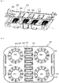
- the figure 4 illustrates an assembly 200 according to an example of the invention.
- the assembly 200 comprises an electrical device 150 for example as illustrated in figure 5 .
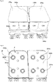
- the electrical device 150 includes electronic components 152,154. Electrical conductors 160p, 160n are fixed on the electronic components 152,154 to connect them electrically.
- the electronic components 152,154 and the electrical conductors 160p, 160n are connected to each other at the level of zones Zf, called fixing zones, visible at figures 6 or 7 .
- These fixing zones Zf may have a height that varies from one zone to another. This is in particular the case when the conductors 160p, 160n are soldered by soldering to the terminals of the electronic components 152,154.
- the thickness of the welds at the Zf fixing zones can vary from one Zf fixing zone to another.
- These fixing zones Zf can also form protrusions relative to the rest of the plate-shaped portion 102.
- the plating member 100 is positioned on a face F, called the plating face, of the electrical device 150. By pressing this plating face F, the plating member 100 is configured to press the electrical device 150 against a surface.
- This plating face comprises in particular said fixing zones Zf.
- the plating member does not take into account the variability of the height of the fixing zones Zf. In doing so, the plating member of the prior art can exert a greater force on a fixing area Zf higher than the others. That causes differentiated wear between the fixing zones.
- each fixing zone Zf comes into a first opening 121 of the plating member 100.
- the plating member 100 does not exert any force directly on the Zf fixing zone, and thus avoids differentiated wear of these Zf fixing zones.
- Each electronic component 152, 154 may comprise two terminals 152p, 154n of the same polarity in the same plane, as for example illustrated in figure 6 .
- the terminals 152p, 154n of an electronic component 152, 154 are at a distance from each other.
- the two corresponding fixing zones Zf are at a distance from each other, for example as illustrated in the figures.
- the plating member 100 comprises two first openings 121 at a distance from each other which each surround a respective fixing zone Zf.
- the second through opening 122 is located equidistant between the first openings 121.
- the second opening 122 comes to press on a middle part of an electronic component 152, 154 so as to improve the plating of the electronic component 152, 154.
- the components electronic 152, 154 are in particular arranged in line one next to the other, so that all of the electrical terminals are distributed on two parallel planes which are opposite. In the figures, the terminals 154p, 154n located in one of these planes are shown.
- the plating face F may include a positive polarity and a negative polarity of the electrical device 150.
- the electronic components 152 on a first side of the row of electronic components are upside down with respect to the electronic components 154 of a second side of the row.
- the first side of the row comprises terminals of opposite polarity to that of the terminals of the second side of the row of electronic components 152, 154.
- An electrical insulation sheet 170p, 170n is notably interposed between the plating member 100 and the plating face F in order to isolate the plating member 100 from the electrical device 150.
- a plate Sufficiently thick insulation is necessary to protect the plating face F from the force exerted by the spring blades.
- the spring blades 110, 116 each exert a lower force compared to the prior art, which makes it possible to use an electrical insulation sheet instead of a plate.
- Such a sheet is flexible while the insulation plate is rigid.
- the electrical insulation sheet has a thickness of 0.5 mm and is in particular made of polyurethane. While in the prior art the electrical insulation plate has a thickness of 2mm and is in particular made of an epoxy resin composite.
- the assembly 200 comprises an electrical insulation sheet, in particular when a single plating member 100 ′ is used to clamp the electrical device 150.
- the plating member is for example such as that illustrated in figure 8 .
- the plating member 100 ' is also similar to the plating member 100 illustrated in the other figures and is used in the same way way.
- one or more electrical insulation sheets 170p, 170n can be used in the case where two tacking members 100 are used to tackle the electrical device 150, for example as illustrated in figure 4 .
- a first part of the plating face F comprises the positive terminals 152p of first electronic components 152 and a second part of the plating face F comprises negative terminals 154n of second electronic components 154.
- the first part of the plating face F is therefore located in the first side of the row of electronic components, and the second part of the plating plate F is located in the second side of the row of electronic components.
- One of the conductors, said positive conductor 160p is connected to the positive terminals 152p of the first electronic components 152.
- a second electrical conductor, said negative conductor 160n is connected to the negative terminals 154n of the second electronic components 154.
- Each electric conductor 160p, 160n comprises an arm which extends between on the one hand the first electronic components 152 and on the other hand the second electronic components 154. These arms are arranged one next to the other, the edges of the electrical conductors 170, 170n are facing.
- the arm of the positive conductor 160p connects to the positive terminals of the second electronic components 154.
- the arm of the negative conductor 160n connects to the negative terminals of the first electronic components 152.
- a first sheet of electrical insulation 170p can be interposed between the plating member 100 and the first part of the plating face F and a second sheet of electrical insulation 170n can be interposed between the plating member 100 and the second part of the plating face F.
- the first sheet of electrical insulation 170p can then extend along the arm of the negative conductor 160n and the second sheet of electrical insulation 170n can then extend along the arm of the positive conductor 160p.
- These electrical insulation sheets 170p, 170n contribute to the electrical insulation of the electrical conductors 170p, 170n at the place where these conductors 160p, 160n are closest, that is to say between the first 152 and the second 154 electronic components.
- the first electrical insulation sheet 170p provides electrical insulation between the portion of the positive conductor 160p included in the plating face F and the arm of the negative conductor 160n.
- the second electrical insulation sheet 170n provides electrical insulation between the portion of the negative conductor 160n included in the plating face F and the arm of the positive conductor 160p.
- the electrical insulation sheets 170n, 170p are therefore integrated into the electronic device 150. To ensure electrical insulation in the plating members 100 and the electrical device 150, these sheets 170n, 170p which are already provided for insulating are therefore used. 160p conductors, 160n between them. Thus, the integration of the assembly 200 is improved.
- the assembly 200 comprises two plating members 100.
- an electrical insulation sheet is interposed between the plating members 100 and the plating face F; in the example illustrated in figure 7 , the plating members 100 come directly against the plating face F of the electrical device 150.
- Each plating member 100 is in contact with a respective polarity of the plating face F.
- the plating members 100 are isolated electrically from each other, for example by a distance between them. Such electrical insulation could be obtained by an insulating material interposed between them.
- the figure 9 represents an electrical equipment 300 comprising an assembly 200 according to an example of the invention.
- the assembly 200 is mounted on a chassis 310 of the electrical equipment 300.
- the plating member 100 is taken in compression between a surface 310a of said chassis 310 and the electrical device 150 so as to press the electrical device 150 against a circuit 312 for cooling the electrical equipment 300.
- This cooling circuit 312 in particular comprises a channel 313 through which a fluid intended to drain the heat from the electrical device 150 circulates.
- the cooling circuit 312 comes in particular against one face of the electrical device 150, said face being opposite to the pressing face F.
- the electrical equipment 300 is for example an inverter on board a vehicle and configured to supply a vehicle engine from a battery.
- the electrical equipment 200 may be a DC-DC voltage converter configured to exchange energy between a high-voltage battery and a low-voltage vehicle battery, or an electric charger configured to charge a high-voltage battery from the vehicle from an electrical network outside the vehicle
- the electrical device is in particular a capacitive block 150 in which the electronic components are capacitors 152, 154.
- the illustrated electrical device 150 could include other electronic components, for example other resistors, or coils inductive.
- the example illustrated comprises several electronic components 152, 154 and two electrical conductors 160p, 160n fixed on the facing face F.
- this example could include a single electronic component 152, 154 and a single electrical conductor 160p, 160n fixed on the plating side F.
Landscapes
- Engineering & Computer Science (AREA)
- Microelectronics & Electronic Packaging (AREA)
- Physics & Mathematics (AREA)
- Thermal Sciences (AREA)
- Structures For Mounting Electric Components On Printed Circuit Boards (AREA)
- Electroplating Methods And Accessories (AREA)
- Connection Of Batteries Or Terminals (AREA)
- Springs (AREA)
Applications Claiming Priority (1)
| Application Number | Priority Date | Filing Date | Title |
|---|---|---|---|
| FR1873801A FR3091013B1 (fr) | 2018-12-21 | 2018-12-21 | Organe de plaquage, ensemble et équipement électrique |
Publications (2)
| Publication Number | Publication Date |
|---|---|
| EP3672382A1 true EP3672382A1 (de) | 2020-06-24 |
| EP3672382B1 EP3672382B1 (de) | 2022-08-03 |
Family
ID=66641086
Family Applications (1)
| Application Number | Title | Priority Date | Filing Date |
|---|---|---|---|
| EP19213473.2A Active EP3672382B1 (de) | 2018-12-21 | 2019-12-04 | Presselement, montage und elektrische ausrüstung |
Country Status (3)
| Country | Link |
|---|---|
| EP (1) | EP3672382B1 (de) |
| CN (1) | CN111356334A (de) |
| FR (1) | FR3091013B1 (de) |
Citations (5)
| Publication number | Priority date | Publication date | Assignee | Title |
|---|---|---|---|---|
| JP2000223630A (ja) * | 1999-02-04 | 2000-08-11 | Sharp Corp | 金属筐体に囲まれた電子部品の放熱構造 |
| DE10142987A1 (de) * | 2001-09-01 | 2003-04-03 | Conti Temic Microelectronic | Wärmeableitelement für elektronische Bauteile |
| JP2005116650A (ja) * | 2003-10-06 | 2005-04-28 | Sanyo Electric Co Ltd | 回路装置 |
| WO2014033382A1 (fr) | 2012-08-29 | 2014-03-06 | Valeo Systemes De Controle Moteur | Organe de plaquage d'une piece sur une surface |
| EP3197035A1 (de) * | 2016-01-20 | 2017-07-26 | Valeo Systemes de Controle Moteur | Elektrische ausstattung, insbesondere für kraftfahrzeug |
Family Cites Families (2)
| Publication number | Priority date | Publication date | Assignee | Title |
|---|---|---|---|---|
| DE102013104949B3 (de) * | 2013-05-14 | 2014-04-24 | Semikron Elektronik Gmbh & Co. Kg | Leistungselektronische Schalteinrichtung und Anordnung hiermit |
| US9564697B2 (en) * | 2014-11-13 | 2017-02-07 | Lear Corporation | Press fit electrical terminal having a solder tab shorter than PCB thickness and method of using same |
-
2018
- 2018-12-21 FR FR1873801A patent/FR3091013B1/fr active Active
-
2019
- 2019-12-04 EP EP19213473.2A patent/EP3672382B1/de active Active
- 2019-12-17 CN CN201911301236.8A patent/CN111356334A/zh active Pending
Patent Citations (5)
| Publication number | Priority date | Publication date | Assignee | Title |
|---|---|---|---|---|
| JP2000223630A (ja) * | 1999-02-04 | 2000-08-11 | Sharp Corp | 金属筐体に囲まれた電子部品の放熱構造 |
| DE10142987A1 (de) * | 2001-09-01 | 2003-04-03 | Conti Temic Microelectronic | Wärmeableitelement für elektronische Bauteile |
| JP2005116650A (ja) * | 2003-10-06 | 2005-04-28 | Sanyo Electric Co Ltd | 回路装置 |
| WO2014033382A1 (fr) | 2012-08-29 | 2014-03-06 | Valeo Systemes De Controle Moteur | Organe de plaquage d'une piece sur une surface |
| EP3197035A1 (de) * | 2016-01-20 | 2017-07-26 | Valeo Systemes de Controle Moteur | Elektrische ausstattung, insbesondere für kraftfahrzeug |
Also Published As
| Publication number | Publication date |
|---|---|
| FR3091013B1 (fr) | 2021-01-15 |
| CN111356334A (zh) | 2020-06-30 |
| FR3091013A1 (fr) | 2020-06-26 |
| EP3672382B1 (de) | 2022-08-03 |
Similar Documents
| Publication | Publication Date | Title |
|---|---|---|
| EP1886401B1 (de) | Elektronikmodul für eine elektrische drehmaschine | |
| FR2886476A1 (fr) | Piece d'interconnexion de puissance pour machine electrique tournante | |
| EP1886395A1 (de) | Signalverbindungsteil für eine elektrische drehmaschine | |
| FR3098078A1 (fr) | Circuit imprimé et procédé pour la mesure de la température dans un connecteur électrique de puissance | |
| FR3062956A1 (fr) | Ensemble de connexion electrique femelle | |
| FR2932318A1 (fr) | Embout de porte-balai et son application a la realisation d'un demarreur pour vehicule automobile | |
| FR3087584A1 (fr) | Dispositif de connexion pour vehicule equipe d'un capteur de temperature | |
| EP3177123B1 (de) | Halterung für elektronische karte, einheit einer solchen elektronischen karte und einer solchen halterung, spannungswandler, der sie umfasst, und elektrische maschine für kraftfahrzeug, die sie umfasst | |
| EP2745661B1 (de) | Elektrische verbindungsvorrichtung, anordnung mit einer solchen vorrichtung und elektronikplatine sowie verfahren zum elektrischen anschluss einer elektronikplatine | |
| EP1912261A1 (de) | Elektrische Anschlussvorrichtung, insbesondere für elektrischen Sonnenkollektor | |
| EP3672382B1 (de) | Presselement, montage und elektrische ausrüstung | |
| EP2891178B1 (de) | Körper zum pressen eines teils auf eine oberfläche | |
| FR3097095A1 (fr) | Équipement electrique comprenant un élément élastique de fixation | |
| EP1933425B1 (de) | Gesicherter elektrischer Kontakt | |
| EP2438651A1 (de) | Einrichtung zum verbinden eines elektrischen verbinders und eines abgeschirmten elektrischen koaxialkabels und entsprechender elektrischer verbinder | |
| FR3089067A1 (fr) | Coffre de batterie et systeme de batterie modulaire | |
| FR3084970A1 (fr) | Equipement electrique | |
| EP3840557B1 (de) | Elektrisches gerät mit einer elektrischen anschlussleiste, die von zwei seiten eines kühlkörpers gekühlt wird | |
| EP2748914A1 (de) | Erdungsschaltung für kohlebürste | |
| FR3060901B1 (fr) | Module electronique de puissance | |
| FR3078149A1 (fr) | Echangeur de chaleur pour composant electrique de vehicule automobile et systeme de regulation thermique associe | |
| WO2023126433A1 (fr) | Ensemble et procédé d'interconnexion électrique | |
| FR2928784A1 (fr) | Dispositif de raccordement electrique notamment pour panneau solaire electrique | |
| EP3331336B1 (de) | Kompaktes leistungselektroniksystem für elektrische motorantriebsanlage | |
| EP3223398B1 (de) | Elektrischer auflader mit einer vorrichtung zur elektrischen verbindung |
Legal Events
| Date | Code | Title | Description |
|---|---|---|---|
| PUAI | Public reference made under article 153(3) epc to a published international application that has entered the european phase |
Free format text: ORIGINAL CODE: 0009012 |
|
| STAA | Information on the status of an ep patent application or granted ep patent |
Free format text: STATUS: THE APPLICATION HAS BEEN PUBLISHED |
|
| AK | Designated contracting states |
Kind code of ref document: A1 Designated state(s): AL AT BE BG CH CY CZ DE DK EE ES FI FR GB GR HR HU IE IS IT LI LT LU LV MC MK MT NL NO PL PT RO RS SE SI SK SM TR |
|
| AX | Request for extension of the european patent |
Extension state: BA ME |
|
| STAA | Information on the status of an ep patent application or granted ep patent |
Free format text: STATUS: REQUEST FOR EXAMINATION WAS MADE |
|
| 17P | Request for examination filed |
Effective date: 20201216 |
|
| RBV | Designated contracting states (corrected) |
Designated state(s): AL AT BE BG CH CY CZ DE DK EE ES FI FR GB GR HR HU IE IS IT LI LT LU LV MC MK MT NL NO PL PT RO RS SE SI SK SM TR |
|
| GRAP | Despatch of communication of intention to grant a patent |
Free format text: ORIGINAL CODE: EPIDOSNIGR1 |
|
| STAA | Information on the status of an ep patent application or granted ep patent |
Free format text: STATUS: GRANT OF PATENT IS INTENDED |
|
| INTG | Intention to grant announced |
Effective date: 20220225 |
|
| GRAS | Grant fee paid |
Free format text: ORIGINAL CODE: EPIDOSNIGR3 |
|
| GRAA | (expected) grant |
Free format text: ORIGINAL CODE: 0009210 |
|
| STAA | Information on the status of an ep patent application or granted ep patent |
Free format text: STATUS: THE PATENT HAS BEEN GRANTED |
|
| AK | Designated contracting states |
Kind code of ref document: B1 Designated state(s): AL AT BE BG CH CY CZ DE DK EE ES FI FR GB GR HR HU IE IS IT LI LT LU LV MC MK MT NL NO PL PT RO RS SE SI SK SM TR |
|
| RIN1 | Information on inventor provided before grant (corrected) |
Inventor name: POUILLY, AURELIEN Inventor name: LEGENDRE, ALEXANDRE |
|
| REG | Reference to a national code |
Ref country code: AT Ref legal event code: REF Ref document number: 1509804 Country of ref document: AT Kind code of ref document: T Effective date: 20220815 Ref country code: CH Ref legal event code: EP |
|
| REG | Reference to a national code |
Ref country code: DE Ref legal event code: R096 Ref document number: 602019017730 Country of ref document: DE |
|
| REG | Reference to a national code |
Ref country code: IE Ref legal event code: FG4D Free format text: LANGUAGE OF EP DOCUMENT: FRENCH |
|
| RAP4 | Party data changed (patent owner data changed or rights of a patent transferred) |
Owner name: VALEO EAUTOMOTIVE FRANCE SAS |
|
| REG | Reference to a national code |
Ref country code: LT Ref legal event code: MG9D |
|
| REG | Reference to a national code |
Ref country code: NL Ref legal event code: MP Effective date: 20220803 |
|
| PG25 | Lapsed in a contracting state [announced via postgrant information from national office to epo] |
Ref country code: SE Free format text: LAPSE BECAUSE OF FAILURE TO SUBMIT A TRANSLATION OF THE DESCRIPTION OR TO PAY THE FEE WITHIN THE PRESCRIBED TIME-LIMIT Effective date: 20220803 Ref country code: RS Free format text: LAPSE BECAUSE OF FAILURE TO SUBMIT A TRANSLATION OF THE DESCRIPTION OR TO PAY THE FEE WITHIN THE PRESCRIBED TIME-LIMIT Effective date: 20220803 Ref country code: PT Free format text: LAPSE BECAUSE OF FAILURE TO SUBMIT A TRANSLATION OF THE DESCRIPTION OR TO PAY THE FEE WITHIN THE PRESCRIBED TIME-LIMIT Effective date: 20221205 Ref country code: NO Free format text: LAPSE BECAUSE OF FAILURE TO SUBMIT A TRANSLATION OF THE DESCRIPTION OR TO PAY THE FEE WITHIN THE PRESCRIBED TIME-LIMIT Effective date: 20221103 Ref country code: NL Free format text: LAPSE BECAUSE OF FAILURE TO SUBMIT A TRANSLATION OF THE DESCRIPTION OR TO PAY THE FEE WITHIN THE PRESCRIBED TIME-LIMIT Effective date: 20220803 Ref country code: LV Free format text: LAPSE BECAUSE OF FAILURE TO SUBMIT A TRANSLATION OF THE DESCRIPTION OR TO PAY THE FEE WITHIN THE PRESCRIBED TIME-LIMIT Effective date: 20220803 Ref country code: LT Free format text: LAPSE BECAUSE OF FAILURE TO SUBMIT A TRANSLATION OF THE DESCRIPTION OR TO PAY THE FEE WITHIN THE PRESCRIBED TIME-LIMIT Effective date: 20220803 Ref country code: FI Free format text: LAPSE BECAUSE OF FAILURE TO SUBMIT A TRANSLATION OF THE DESCRIPTION OR TO PAY THE FEE WITHIN THE PRESCRIBED TIME-LIMIT Effective date: 20220803 Ref country code: ES Free format text: LAPSE BECAUSE OF FAILURE TO SUBMIT A TRANSLATION OF THE DESCRIPTION OR TO PAY THE FEE WITHIN THE PRESCRIBED TIME-LIMIT Effective date: 20220803 |
|
| REG | Reference to a national code |
Ref country code: AT Ref legal event code: MK05 Ref document number: 1509804 Country of ref document: AT Kind code of ref document: T Effective date: 20220803 |
|
| PG25 | Lapsed in a contracting state [announced via postgrant information from national office to epo] |
Ref country code: PL Free format text: LAPSE BECAUSE OF FAILURE TO SUBMIT A TRANSLATION OF THE DESCRIPTION OR TO PAY THE FEE WITHIN THE PRESCRIBED TIME-LIMIT Effective date: 20220803 Ref country code: IS Free format text: LAPSE BECAUSE OF FAILURE TO SUBMIT A TRANSLATION OF THE DESCRIPTION OR TO PAY THE FEE WITHIN THE PRESCRIBED TIME-LIMIT Effective date: 20221203 Ref country code: HR Free format text: LAPSE BECAUSE OF FAILURE TO SUBMIT A TRANSLATION OF THE DESCRIPTION OR TO PAY THE FEE WITHIN THE PRESCRIBED TIME-LIMIT Effective date: 20220803 Ref country code: GR Free format text: LAPSE BECAUSE OF FAILURE TO SUBMIT A TRANSLATION OF THE DESCRIPTION OR TO PAY THE FEE WITHIN THE PRESCRIBED TIME-LIMIT Effective date: 20221104 |
|
| PG25 | Lapsed in a contracting state [announced via postgrant information from national office to epo] |
Ref country code: SM Free format text: LAPSE BECAUSE OF FAILURE TO SUBMIT A TRANSLATION OF THE DESCRIPTION OR TO PAY THE FEE WITHIN THE PRESCRIBED TIME-LIMIT Effective date: 20220803 Ref country code: RO Free format text: LAPSE BECAUSE OF FAILURE TO SUBMIT A TRANSLATION OF THE DESCRIPTION OR TO PAY THE FEE WITHIN THE PRESCRIBED TIME-LIMIT Effective date: 20220803 Ref country code: DK Free format text: LAPSE BECAUSE OF FAILURE TO SUBMIT A TRANSLATION OF THE DESCRIPTION OR TO PAY THE FEE WITHIN THE PRESCRIBED TIME-LIMIT Effective date: 20220803 Ref country code: CZ Free format text: LAPSE BECAUSE OF FAILURE TO SUBMIT A TRANSLATION OF THE DESCRIPTION OR TO PAY THE FEE WITHIN THE PRESCRIBED TIME-LIMIT Effective date: 20220803 Ref country code: AT Free format text: LAPSE BECAUSE OF FAILURE TO SUBMIT A TRANSLATION OF THE DESCRIPTION OR TO PAY THE FEE WITHIN THE PRESCRIBED TIME-LIMIT Effective date: 20220803 |
|
| REG | Reference to a national code |
Ref country code: DE Ref legal event code: R097 Ref document number: 602019017730 Country of ref document: DE |
|
| PG25 | Lapsed in a contracting state [announced via postgrant information from national office to epo] |
Ref country code: SK Free format text: LAPSE BECAUSE OF FAILURE TO SUBMIT A TRANSLATION OF THE DESCRIPTION OR TO PAY THE FEE WITHIN THE PRESCRIBED TIME-LIMIT Effective date: 20220803 Ref country code: EE Free format text: LAPSE BECAUSE OF FAILURE TO SUBMIT A TRANSLATION OF THE DESCRIPTION OR TO PAY THE FEE WITHIN THE PRESCRIBED TIME-LIMIT Effective date: 20220803 |
|
| PLBE | No opposition filed within time limit |
Free format text: ORIGINAL CODE: 0009261 |
|
| STAA | Information on the status of an ep patent application or granted ep patent |
Free format text: STATUS: NO OPPOSITION FILED WITHIN TIME LIMIT |
|
| PG25 | Lapsed in a contracting state [announced via postgrant information from national office to epo] |
Ref country code: AL Free format text: LAPSE BECAUSE OF FAILURE TO SUBMIT A TRANSLATION OF THE DESCRIPTION OR TO PAY THE FEE WITHIN THE PRESCRIBED TIME-LIMIT Effective date: 20220803 |
|
| 26N | No opposition filed |
Effective date: 20230504 |
|
| REG | Reference to a national code |
Ref country code: CH Ref legal event code: PL |
|
| P01 | Opt-out of the competence of the unified patent court (upc) registered |
Effective date: 20230629 |
|
| REG | Reference to a national code |
Ref country code: BE Ref legal event code: MM Effective date: 20221231 |
|
| PG25 | Lapsed in a contracting state [announced via postgrant information from national office to epo] |
Ref country code: SI Free format text: LAPSE BECAUSE OF FAILURE TO SUBMIT A TRANSLATION OF THE DESCRIPTION OR TO PAY THE FEE WITHIN THE PRESCRIBED TIME-LIMIT Effective date: 20220803 Ref country code: LU Free format text: LAPSE BECAUSE OF NON-PAYMENT OF DUE FEES Effective date: 20221204 |
|
| PG25 | Lapsed in a contracting state [announced via postgrant information from national office to epo] |
Ref country code: LI Free format text: LAPSE BECAUSE OF NON-PAYMENT OF DUE FEES Effective date: 20221231 Ref country code: IE Free format text: LAPSE BECAUSE OF NON-PAYMENT OF DUE FEES Effective date: 20221204 Ref country code: CH Free format text: LAPSE BECAUSE OF NON-PAYMENT OF DUE FEES Effective date: 20221231 |
|
| PG25 | Lapsed in a contracting state [announced via postgrant information from national office to epo] |
Ref country code: BE Free format text: LAPSE BECAUSE OF NON-PAYMENT OF DUE FEES Effective date: 20221231 |
|
| PGFP | Annual fee paid to national office [announced via postgrant information from national office to epo] |
Ref country code: GB Payment date: 20231221 Year of fee payment: 5 |
|
| PGFP | Annual fee paid to national office [announced via postgrant information from national office to epo] |
Ref country code: FR Payment date: 20231220 Year of fee payment: 5 Ref country code: DE Payment date: 20231208 Year of fee payment: 5 |
|
| PG25 | Lapsed in a contracting state [announced via postgrant information from national office to epo] |
Ref country code: HU Free format text: LAPSE BECAUSE OF FAILURE TO SUBMIT A TRANSLATION OF THE DESCRIPTION OR TO PAY THE FEE WITHIN THE PRESCRIBED TIME-LIMIT; INVALID AB INITIO Effective date: 20191204 |
|
| PG25 | Lapsed in a contracting state [announced via postgrant information from national office to epo] |
Ref country code: CY Free format text: LAPSE BECAUSE OF FAILURE TO SUBMIT A TRANSLATION OF THE DESCRIPTION OR TO PAY THE FEE WITHIN THE PRESCRIBED TIME-LIMIT Effective date: 20220803 |