EP3671960A1 - Leiteranschlusskontakt und leiterplattenanordnung - Google Patents
Leiteranschlusskontakt und leiterplattenanordnung Download PDFInfo
- Publication number
- EP3671960A1 EP3671960A1 EP20157193.2A EP20157193A EP3671960A1 EP 3671960 A1 EP3671960 A1 EP 3671960A1 EP 20157193 A EP20157193 A EP 20157193A EP 3671960 A1 EP3671960 A1 EP 3671960A1
- Authority
- EP
- European Patent Office
- Prior art keywords
- connection
- contact
- conductor
- circuit board
- printed circuit
- Prior art date
- Legal status (The legal status is an assumption and is not a legal conclusion. Google has not performed a legal analysis and makes no representation as to the accuracy of the status listed.)
- Withdrawn
Links
Images






Classifications
-
- H—ELECTRICITY
- H01—ELECTRIC ELEMENTS
- H01R—ELECTRICALLY-CONDUCTIVE CONNECTIONS; STRUCTURAL ASSOCIATIONS OF A PLURALITY OF MUTUALLY-INSULATED ELECTRICAL CONNECTING ELEMENTS; COUPLING DEVICES; CURRENT COLLECTORS
- H01R4/00—Electrically-conductive connections between two or more conductive members in direct contact, i.e. touching one another; Means for effecting or maintaining such contact; Electrically-conductive connections having two or more spaced connecting locations for conductors and using contact members penetrating insulation
- H01R4/28—Clamped connections, spring connections
- H01R4/48—Clamped connections, spring connections utilising a spring, clip, or other resilient member
- H01R4/4809—Clamped connections, spring connections utilising a spring, clip, or other resilient member using a leaf spring to bias the conductor toward the busbar
- H01R4/48185—Clamped connections, spring connections utilising a spring, clip, or other resilient member using a leaf spring to bias the conductor toward the busbar adapted for axial insertion of a wire end
-
- F—MECHANICAL ENGINEERING; LIGHTING; HEATING; WEAPONS; BLASTING
- F21—LIGHTING
- F21V—FUNCTIONAL FEATURES OR DETAILS OF LIGHTING DEVICES OR SYSTEMS THEREOF; STRUCTURAL COMBINATIONS OF LIGHTING DEVICES WITH OTHER ARTICLES, NOT OTHERWISE PROVIDED FOR
- F21V23/00—Arrangement of electric circuit elements in or on lighting devices
- F21V23/06—Arrangement of electric circuit elements in or on lighting devices the elements being coupling devices, e.g. connectors
-
- H—ELECTRICITY
- H01—ELECTRIC ELEMENTS
- H01R—ELECTRICALLY-CONDUCTIVE CONNECTIONS; STRUCTURAL ASSOCIATIONS OF A PLURALITY OF MUTUALLY-INSULATED ELECTRICAL CONNECTING ELEMENTS; COUPLING DEVICES; CURRENT COLLECTORS
- H01R12/00—Structural associations of a plurality of mutually-insulated electrical connecting elements, specially adapted for printed circuits, e.g. printed circuit boards [PCB], flat or ribbon cables, or like generally planar structures, e.g. terminal strips, terminal blocks; Coupling devices specially adapted for printed circuits, flat or ribbon cables, or like generally planar structures; Terminals specially adapted for contact with, or insertion into, printed circuits, flat or ribbon cables, or like generally planar structures
- H01R12/50—Fixed connections
- H01R12/51—Fixed connections for rigid printed circuits or like structures
- H01R12/53—Fixed connections for rigid printed circuits or like structures connecting to cables except for flat or ribbon cables
-
- H—ELECTRICITY
- H01—ELECTRIC ELEMENTS
- H01R—ELECTRICALLY-CONDUCTIVE CONNECTIONS; STRUCTURAL ASSOCIATIONS OF A PLURALITY OF MUTUALLY-INSULATED ELECTRICAL CONNECTING ELEMENTS; COUPLING DEVICES; CURRENT COLLECTORS
- H01R12/00—Structural associations of a plurality of mutually-insulated electrical connecting elements, specially adapted for printed circuits, e.g. printed circuit boards [PCB], flat or ribbon cables, or like generally planar structures, e.g. terminal strips, terminal blocks; Coupling devices specially adapted for printed circuits, flat or ribbon cables, or like generally planar structures; Terminals specially adapted for contact with, or insertion into, printed circuits, flat or ribbon cables, or like generally planar structures
- H01R12/50—Fixed connections
- H01R12/51—Fixed connections for rigid printed circuits or like structures
- H01R12/55—Fixed connections for rigid printed circuits or like structures characterised by the terminals
- H01R12/57—Fixed connections for rigid printed circuits or like structures characterised by the terminals surface mounting terminals
-
- H—ELECTRICITY
- H01—ELECTRIC ELEMENTS
- H01R—ELECTRICALLY-CONDUCTIVE CONNECTIONS; STRUCTURAL ASSOCIATIONS OF A PLURALITY OF MUTUALLY-INSULATED ELECTRICAL CONNECTING ELEMENTS; COUPLING DEVICES; CURRENT COLLECTORS
- H01R12/00—Structural associations of a plurality of mutually-insulated electrical connecting elements, specially adapted for printed circuits, e.g. printed circuit boards [PCB], flat or ribbon cables, or like generally planar structures, e.g. terminal strips, terminal blocks; Coupling devices specially adapted for printed circuits, flat or ribbon cables, or like generally planar structures; Terminals specially adapted for contact with, or insertion into, printed circuits, flat or ribbon cables, or like generally planar structures
- H01R12/70—Coupling devices
- H01R12/7005—Guiding, mounting, polarizing or locking means; Extractors
- H01R12/7011—Locking or fixing a connector to a PCB
- H01R12/707—Soldering or welding
-
- H—ELECTRICITY
- H01—ELECTRIC ELEMENTS
- H01R—ELECTRICALLY-CONDUCTIVE CONNECTIONS; STRUCTURAL ASSOCIATIONS OF A PLURALITY OF MUTUALLY-INSULATED ELECTRICAL CONNECTING ELEMENTS; COUPLING DEVICES; CURRENT COLLECTORS
- H01R12/00—Structural associations of a plurality of mutually-insulated electrical connecting elements, specially adapted for printed circuits, e.g. printed circuit boards [PCB], flat or ribbon cables, or like generally planar structures, e.g. terminal strips, terminal blocks; Coupling devices specially adapted for printed circuits, flat or ribbon cables, or like generally planar structures; Terminals specially adapted for contact with, or insertion into, printed circuits, flat or ribbon cables, or like generally planar structures
- H01R12/70—Coupling devices
- H01R12/71—Coupling devices for rigid printing circuits or like structures
- H01R12/72—Coupling devices for rigid printing circuits or like structures coupling with the edge of the rigid printed circuits or like structures
- H01R12/722—Coupling devices for rigid printing circuits or like structures coupling with the edge of the rigid printed circuits or like structures coupling devices mounted on the edge of the printed circuits
- H01R12/728—Coupling devices without an insulating housing provided on the edge of the PCB
-
- H—ELECTRICITY
- H01—ELECTRIC ELEMENTS
- H01R—ELECTRICALLY-CONDUCTIVE CONNECTIONS; STRUCTURAL ASSOCIATIONS OF A PLURALITY OF MUTUALLY-INSULATED ELECTRICAL CONNECTING ELEMENTS; COUPLING DEVICES; CURRENT COLLECTORS
- H01R12/00—Structural associations of a plurality of mutually-insulated electrical connecting elements, specially adapted for printed circuits, e.g. printed circuit boards [PCB], flat or ribbon cables, or like generally planar structures, e.g. terminal strips, terminal blocks; Coupling devices specially adapted for printed circuits, flat or ribbon cables, or like generally planar structures; Terminals specially adapted for contact with, or insertion into, printed circuits, flat or ribbon cables, or like generally planar structures
- H01R12/70—Coupling devices
- H01R12/71—Coupling devices for rigid printing circuits or like structures
- H01R12/72—Coupling devices for rigid printing circuits or like structures coupling with the edge of the rigid printed circuits or like structures
- H01R12/73—Coupling devices for rigid printing circuits or like structures coupling with the edge of the rigid printed circuits or like structures connecting to other rigid printed circuits or like structures
- H01R12/732—Printed circuits being in the same plane
-
- H—ELECTRICITY
- H01—ELECTRIC ELEMENTS
- H01R—ELECTRICALLY-CONDUCTIVE CONNECTIONS; STRUCTURAL ASSOCIATIONS OF A PLURALITY OF MUTUALLY-INSULATED ELECTRICAL CONNECTING ELEMENTS; COUPLING DEVICES; CURRENT COLLECTORS
- H01R4/00—Electrically-conductive connections between two or more conductive members in direct contact, i.e. touching one another; Means for effecting or maintaining such contact; Electrically-conductive connections having two or more spaced connecting locations for conductors and using contact members penetrating insulation
- H01R4/02—Soldered or welded connections
- H01R4/023—Soldered or welded connections between cables or wires and terminals
-
- H—ELECTRICITY
- H01—ELECTRIC ELEMENTS
- H01R—ELECTRICALLY-CONDUCTIVE CONNECTIONS; STRUCTURAL ASSOCIATIONS OF A PLURALITY OF MUTUALLY-INSULATED ELECTRICAL CONNECTING ELEMENTS; COUPLING DEVICES; CURRENT COLLECTORS
- H01R4/00—Electrically-conductive connections between two or more conductive members in direct contact, i.e. touching one another; Means for effecting or maintaining such contact; Electrically-conductive connections having two or more spaced connecting locations for conductors and using contact members penetrating insulation
- H01R4/24—Connections using contact members penetrating or cutting insulation or cable strands
- H01R4/2416—Connections using contact members penetrating or cutting insulation or cable strands the contact members having insulation-cutting edges, e.g. of tuning fork type
- H01R4/242—Connections using contact members penetrating or cutting insulation or cable strands the contact members having insulation-cutting edges, e.g. of tuning fork type the contact members being plates having a single slot
-
- H—ELECTRICITY
- H01—ELECTRIC ELEMENTS
- H01R—ELECTRICALLY-CONDUCTIVE CONNECTIONS; STRUCTURAL ASSOCIATIONS OF A PLURALITY OF MUTUALLY-INSULATED ELECTRICAL CONNECTING ELEMENTS; COUPLING DEVICES; CURRENT COLLECTORS
- H01R4/00—Electrically-conductive connections between two or more conductive members in direct contact, i.e. touching one another; Means for effecting or maintaining such contact; Electrically-conductive connections having two or more spaced connecting locations for conductors and using contact members penetrating insulation
- H01R4/24—Connections using contact members penetrating or cutting insulation or cable strands
- H01R4/2416—Connections using contact members penetrating or cutting insulation or cable strands the contact members having insulation-cutting edges, e.g. of tuning fork type
- H01R4/242—Connections using contact members penetrating or cutting insulation or cable strands the contact members having insulation-cutting edges, e.g. of tuning fork type the contact members being plates having a single slot
- H01R4/2425—Flat plates, e.g. multi-layered flat plates
-
- H—ELECTRICITY
- H01—ELECTRIC ELEMENTS
- H01R—ELECTRICALLY-CONDUCTIVE CONNECTIONS; STRUCTURAL ASSOCIATIONS OF A PLURALITY OF MUTUALLY-INSULATED ELECTRICAL CONNECTING ELEMENTS; COUPLING DEVICES; CURRENT COLLECTORS
- H01R4/00—Electrically-conductive connections between two or more conductive members in direct contact, i.e. touching one another; Means for effecting or maintaining such contact; Electrically-conductive connections having two or more spaced connecting locations for conductors and using contact members penetrating insulation
- H01R4/28—Clamped connections, spring connections
- H01R4/48—Clamped connections, spring connections utilising a spring, clip, or other resilient member
-
- H—ELECTRICITY
- H01—ELECTRIC ELEMENTS
- H01R—ELECTRICALLY-CONDUCTIVE CONNECTIONS; STRUCTURAL ASSOCIATIONS OF A PLURALITY OF MUTUALLY-INSULATED ELECTRICAL CONNECTING ELEMENTS; COUPLING DEVICES; CURRENT COLLECTORS
- H01R4/00—Electrically-conductive connections between two or more conductive members in direct contact, i.e. touching one another; Means for effecting or maintaining such contact; Electrically-conductive connections having two or more spaced connecting locations for conductors and using contact members penetrating insulation
- H01R4/28—Clamped connections, spring connections
- H01R4/48—Clamped connections, spring connections utilising a spring, clip, or other resilient member
- H01R4/4809—Clamped connections, spring connections utilising a spring, clip, or other resilient member using a leaf spring to bias the conductor toward the busbar
- H01R4/48185—Clamped connections, spring connections utilising a spring, clip, or other resilient member using a leaf spring to bias the conductor toward the busbar adapted for axial insertion of a wire end
- H01R4/4819—Clamped connections, spring connections utilising a spring, clip, or other resilient member using a leaf spring to bias the conductor toward the busbar adapted for axial insertion of a wire end the spring shape allowing insertion of the conductor end when the spring is unbiased
- H01R4/4823—Multiblade spring
-
- H—ELECTRICITY
- H01—ELECTRIC ELEMENTS
- H01R—ELECTRICALLY-CONDUCTIVE CONNECTIONS; STRUCTURAL ASSOCIATIONS OF A PLURALITY OF MUTUALLY-INSULATED ELECTRICAL CONNECTING ELEMENTS; COUPLING DEVICES; CURRENT COLLECTORS
- H01R4/00—Electrically-conductive connections between two or more conductive members in direct contact, i.e. touching one another; Means for effecting or maintaining such contact; Electrically-conductive connections having two or more spaced connecting locations for conductors and using contact members penetrating insulation
- H01R4/28—Clamped connections, spring connections
- H01R4/50—Clamped connections, spring connections utilising a cam, wedge, cone or ball also combined with a screw
- H01R4/5083—Clamped connections, spring connections utilising a cam, wedge, cone or ball also combined with a screw using a wedge
Definitions
- the invention relates to a conductor connection contact with a solder connection surface for connection to a printed circuit board and a plug contact connection with a spring clamp element.
- the invention further relates to a circuit board arrangement with a circuit board, a conductor connection contact being soldered to the circuit board with its soldering areas.
- Printed circuit boards with electrical / electronic components mounted on them have conductor connection contacts for the electrically conductive connection of conductors or for connecting adjacent printed circuit boards to one another. These are soldered onto the PCB in a push-through or surface mounting and connected to it electrically and mechanically.
- DE 200 01 510 U1 shows a connection device for electrical conductors with insulation displacement contact connections soldered onto a circuit board.
- a contact element is designed as a sheet metal stamped / bent part and has two mutually parallel pairs of contact cutting edges that widen in the manner of an opening in their end region to cut open the insulation of an electrical conductor to be clamped on.
- the contact blades of each pair of contact blades are separated from one another by slots.
- the two pairs of contact blades are connected to one another via lateral webs.
- Several such cutting contact elements are connected to one another in a band-like manner for assembly on the printed circuit board.
- EP 0 043 165 A1 shows an insulation displacement contact with two conductor connection areas aligned transversely to one another.
- the conductor connection areas are each formed by clamping slots on opposite walls, the walls being folded over into a box.
- DE 10 2006 052 119 A1 discloses an insulation displacement connection with a first insulation displacement element attached to a first component and a second insulation displacement element attached to a second component.
- the two insulation displacement elements can be pushed into one another in the joining direction and can be displaced relative to one another transversely to the joining direction.
- DE 196 17 259 A1 discloses an electrical terminal with an upwardly open insulation displacement contact and further plug contacts which are arranged in the lower part of the terminal.
- the clamp is made in one piece from a band-shaped metal strip, one end piece of the strip material being divided into several tongues, one of which, as an anchor end piece, stabilizes the shape of the clamp and the other, as leaf spring end pieces, form the insulation displacement contacts .
- Printed circuit board solder pins protrude from a bottom surface which connects the insulation displacement contact and the leaf spring end piece.
- DE 195 12 221 A1 shows an electrical terminal block for printed circuit boards with a bridging rail which can be plugged onto solder connection pins.
- the bridging rail is designed as an essentially planar, flat bridging band which has push-through slots which are formed by two resilient tongues punched out of the bridging band.
- connection surface has a plug opening and at least one spring-elastic clamping tongue to form the spring clamping element. This enables the simple connection of an electrical conductor which is inserted through the plug-in opening and clamped to the connection surface of the plug-in contact connection by means of the spring-elastic clamping tongue.
- connection area then merges into a foot region, which is in each case connected to a solder connection area or has a solder connection area on its side facing away from the connection area.
- connection area is stably supported at a distance from the plane of the printed circuit board with the aid of the foot regions.
- the solder connection areas adjoining the foot areas ensure that the plug contact connection is kept stable on the solder connection areas when the solder connection contact is soldered to a printed circuit board.
- the current flow then goes through the foot areas directly to the solder connection surface, so that the current-conducting cross-sections and paths are optimized.
- resilient clamping tongues can be bent out to point towards each other.
- the freely movable ends of the clamping tongues then form clamping edges for clamping an electrical conductor or contact pin inserted into the insertion opening.
- An electrical conductor or contact pin can thus be connected very reliably with an extremely simple construction of the conductor connection contact.
- the current paths then lead the shortest way over the clamping tongues and the foot sections to the solder connection areas.
- An insulation displacement contact connection can also be present on the conductor connection contact.
- a solder connection surface can be arranged between an insulation displacement contact connection and a web leading to the connection level. This has the advantage that the insulation displacement contact connection and the connection surface are connected to one another via the common solder connection surface, the current paths between insulation displacement connection contact terminal and plug contact connection being short and the insulation displacement contact connection and the plug contact connection via the common solder connection surface are mechanically stabilized.
- the insulation displacement contact connection can have two spaced-apart contact fingers which are connected to one another in a common root section.
- the root section then merges into the foot section or forms the foot section. It is conceivable that the root section merges into one of the solder connection surfaces. This then leads to a very compact structure of the solder connection contact.
- the direction of extension of a wire bridge clamped to the insulation displacement contact connection in the clamping region on the insulation displacement contact connection can be oriented transversely to the direction of insertion of the plug contact connection.
- the direction of extension of the wire bridge at the insulation displacement contact connection in the region of the clamping point, in which a wire bridge is guided to the clamping point between the contact fingers, runs in the plugging direction of the plug contact connection.
- the plane spanned by contact fingers of the cutting plug contact connection or a slotted wall to form the cutting plug contact connection is thus oriented transversely to the plane of the connection surface.
- Transversal means an orientation in the angular range of 90 ° +/- 20 ° and preferably 90 ° +/- 5 °.
- the direction of extension of the wire bridge clamped to the insulation displacement contact connection in the clamping region of this insulation displacement contact connection can be in the direction of extension of the connection surface or also transverse to the direction of extension of the connection surface. However, it is also conceivable that it is oriented obliquely to the direction of extension of the connection surface.
- the circuit board arrangement has a circuit board in which such a conductor connection contact is soldered onto the circuit board with its soldering areas. The circuit board then has a conductor lead-through opening below the plug-in opening, so that an electrical conductor can be inserted through the conductor lead-through opening into the plug-in opening and clamped on the plug contact connection. This enables a very compact connection of an electrical conductor to the circuit board with a plug-in direction perpendicular to the circuit board.
- connection area of the conductor connection contact can extend parallel to the plane of the circuit board. A section of the conductor connection contact having the insulation displacement contact connection then protrudes from the plane of the circuit board.
- a material flap can be spaced from the connection surface to one of the solder connection surfaces, e.g. protrude in the direction of an insulation displacement contact connection.
- the connection area adjacent to the plug contact connection is thus enlarged.
- This material flap also known as a flap
- the clamping spring tongues can have a kink or a bend in an area upstream of the respective clamping edge.
- the clamping tongues bent out toward one another are oriented at a greater angle to one another in the regions adjacent to the connection surface than in the region adjacent to the clamping edge. Due to the kink or the bend, the surfaces of the opposing clamping tongues adjoining the clamping edges are thus arranged at an acute angle to one another.
- the direction of insertion for inserting an electrical conductor into the plug contact connection is substantially perpendicular to the spatial extent of at least one of the solder connection surfaces. In this way, the electrical conductor can be conveniently inserted into the plug contact connection transversely to the spatial extent of the printed circuit board from the top or the bottom.
- a resilient clamping tongue is arranged on an edge of the plug-in opening and a conductor insertion tongue is arranged on an edge of the plug-in opening opposite this edge, the clamping tongue and the conductor insertion tongue being bent away from each other.
- the conductor insertion tongue can form a conductor insertion slope for the simplified insertion of an electrical conductor to a clamping point formed with a freely movable end of the clamping tongue.
- the conductor insertion tongue is not necessarily part of the clamping point itself or does not necessarily have to form a counter bearing when the electrical conductor is clamped by the clamping tongue.
- the counter bearing can e.g. be formed by the connection surface of the conductor connection contact.
- the conductor connection contact has a further plug contact connection, the insertion direction of which for inserting a conductor into the further plug connection is essentially orthogonal to an insertion direction of the plug contact connection formed on the connection surface.
- the further plug contact connection can e.g. be formed on a foot section of the conductor connection contact.
- the conductor connection contact can also have a plurality of further plug contact connections with the mentioned orthogonal insertion direction, e.g. one or more such plug contact connections in each of the foot sections. In this way e.g. looping through an electrical potential can be realized from one circuit board to the next circuit board.
- circuit boards By combining a vertical and a horizontal conductor connection on one and the same conductor connection contact, e.g. an SMD terminal, circuit boards can be wired both vertically (from the back of the circuit board) and horizontally (on the top of the circuit board). This means that no circuit boards for the respective application need to be manufactured with specially shaped conductor connection contacts. Instead, a circuit board can be manufactured and used for both types of wiring. For example, luminaire manufacturers can use a single LED module with such a conductor connection contact for luminaires wired on the front and rear.
- the insertion direction of the first-mentioned plug contact connection which is formed on the connection surface of the conductor connection contact, can optionally point towards the front or the back of the circuit board, i.e. from the side of the conductor connection contact on which the foot sections protrude from the connection area, or from the opposite side of the connection area. Wiring can thus also be made possible for both contacting directions on the top side of the printed circuit board.
- the further plug contact connection can permit wiring on the top side of the printed circuit board or on the underside of the printed circuit board, depending on which side the solder connection surface is formed on.
- the conductor connection contact can also be provided with solder connection surfaces on both sides be formed so that either the conductor connection contact protrudes from one side of the circuit board and is not passed through an opening in the circuit board, or is passed through an opening in the circuit board and protrudes on the opposite side of the circuit board.
- the circuit board arrangement can have a plurality of circuit boards which are arranged adjacent to one another.
- the conductor connection contacts are then arranged diagonally offset from one another on opposite edge regions of the printed circuit board.
- the adjacent circuit boards can thus be connected to one another in an electrically conductive manner by means of wire bridges, which extend between the conductor connection contacts lying opposite one another.
- the diagonally offset arrangement of the conductor connection contacts then leads the wire bridges over several bends, so that sufficient tolerance compensation for thermal expansion is ensured. Due to the diagonally offset arrangement of the conductor connection contacts, a point or mirror symmetrical arrangement of the conductor connection contacts on a circuit board is also possible. For example, conductor terminal contacts are arranged symmetrically and diagonally offset from one another on opposite edge regions of a printed circuit board.
- a wire bridge in the sense of the present invention is understood to mean an electrical line that can be clamped into the insulation displacement contact connection, such as in particular a non-insulated wire piece, an insulated electrical conductor (rigid or flexible) or also a conductor rail piece with e.g. rectangular cross section.
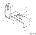
- Figure 1a shows a perspective view of a first embodiment of a conductor connection contact 1, which is formed in one piece from a piece of sheet material as a stamped and bent part.
- the conductor connection contact 1 has an insulation displacement contact connection 2 at one end.
- This insulation displacement contact connection 2 is formed from two contact fingers 3, which are aligned parallel to one another with an intermediate clamping slot 4 on a common plane and are connected to one another via a common root region 5.
- the free end sections of the contact fingers 3 are formed in a funnel-shaped manner toward the root region 5, for example by an inlet slope 6, so that the insertion of a wire bridge into the clamping slot 4 is facilitated.
- the mutually facing inner edges 7 of the contact fingers 3 clamp a wire bridge between them due to the spring force of the contact fingers 3 and the adjacent root section 5. They are designed as cut contacts at least to such an extent that the contact fingers 3 dig into the surface of an inserted wire bridge. However, they can also be sharp-edged in order to cut open an insulating jacket of a wire bridge, for example an insulated rigid or flexible electrical conductor, when inserted into the insulation displacement contact 2, in order in this way to expose the electrically conductive part of the wire bridge and to conduct it electrically to contact the contact fingers 3.
- connection contact 1 has a plug contact connection 8 on a connection surface 9.
- This connection surface 9 has a plug opening 10 and spring-elastic clamping tongues 11, which from the level of Pad 9 and out of the plug opening 10 and protrude towards each other.
- the clamping tongues 11 are cut or punched out of the sheet metal material of the connection surface 9 and protrude from opposite edge edges of the insertion opening 10.
- the insertion opening 10 is then delimited by opposite side webs 12.
- the conductor connection contact 1 has two solder connection surfaces 13a, 13b. It can be seen that the connection surface 9 lies on a level above the plane spanned by the solder connection surfaces 13a, 13b. Between the connection surface 9 and the solder connection surfaces 13a, 13b, foot sections 14 are provided, which connect to the connection surface 9 and lead to a respective solder connection surface 13a, 13b. In the exemplary embodiment shown, these foot sections 14 are designed as webs folded over from the connection surface 9. These are bent approximately at right angles from the connection surface 9.
- solder connection surfaces 13a, 13b can be formed at the end of the foot sections 14 or, as in the case of the solder connection surface 13a, merge from the foot section 14 into a solder connection surface 13a after a further bend.
- connection surface 13a merges into the insulation displacement contact connection 2 or its root section 5.
- This root section 5 with the adjoining contact fingers 3 extends approximately parallel to the foot section 14, so that the insulation displacement contact connection 2 and the foot section 14 are approximately perpendicular to the solder connection surface connecting the insulation displacement contact connection 2 to the foot section 14 13a stand.
- the connection surface 9, on the other hand, lies on a plane that lies transversely to the plane of extent of the insulation displacement contact connection 2.
- the insulation displacement contact connection 2 is thus aligned on a level that is perpendicular to the level of the connection surface 9.
- the plane of the connection surface 9 is at an angle of 90 ° +/- 45 ° to the plane of the insulation displacement contact connection 2.
- the conductor connection contact 1 can be stably soldered onto a circuit board. With the help of the transition from the first soldering connection surface 13a to the insulation displacement contact connection 2 projecting therefrom, this is also stably connected to a printed circuit board with short current paths.
- Figure 1b shows a compared to the embodiment of Figure 1a ) somewhat modified variant of the conductor connection contact 1.
- a material flap 3 is provided on the connection surface 9 at a distance from the horizontal solder connection surface 13a, which is cut free from the bend which merges into the foot section 14 and enlarges the flat surface of the connection surface 9 in the region of the bend. This increases the suction area for the automatic handling and assembly of the conductor connection contact 1.
- the material tab 33 is provided on the side of the insulation displacement contact connection 2 and extends in the direction of this insulation displacement contact connection 2.
- such a material tab 33 on the opposite side at a distance from the solder connection surface 13b) is present or that such cloths are provided on both sides. This also depends specifically on the position of the plug opening 10 on the connection surface 9.
- solder connection surface 13b) merges into a bend on the right side from the foot section 14 and provides a flat support.
- This solder connection surface 13b) is therefore not as in FIG Figure 1a ) formed only by the lower edge of the foot section 14, but by a surface section extending transversely from the foot section 14 after a bend.
- the insulation displacement contact connection 2 is also made in comparison to the embodiment Figure 1a ) slightly modified. It becomes clear that the outer edges of the contact fingers 3, which are each opposite the clamping slot 4, are concavely curved toward the clamping slot. This is the width of the insulation displacement contact connection 2 in the area of the contact slot is lower than in the area of the inlet slopes 6. In this way, the spring force of the contact fingers 3 can be improved.
- connection area 9 is spaced from the plane of the solder connection areas 13a, 13b, which is achieved by the foot areas 14. It can also be seen that the insulation displacement contact connection 2 lies on a plane which is transverse to the plane of the connection surface 9.
- the clamping tongues 11 of the spring clamping element are bent toward one another out of the plane of the connection surface 9 and away from the plane of the solder connection surfaces 13a, 13b.
- the freely movable ends of the resilient clamping tongues 11 have clamping edges 15 to form a plug contact in order to clamp an electrical conductor or contact pin inserted between them in the plug-in opening 10 in the plug-in direction S and thus to make electrical contact therewith.
- Figure 2b omits a side view of the modified conductor connection contact 1 Figure 1b ) detect. It is clear here that the material flap 33 extends at a distance from the soldering connection surface 13a on the level of the connection surface 9 in the direction of the insulation displacement contact connection 2, so as to enlarge the suction surface for an automatic handling machine.
- solder connection surface 13b is not simply formed from the lower edge of the foot section 4, but rather from a surface section which extends away from the foot section 4.
- the contact fingers 3 of the insulation displacement connection taper conically in terms of their width towards the free end. This means that the material thickness of the contact fingers 3 decreases towards their free end.
- Figure 3 omits a front view of the conductor connection contact 1 Figures 1a and 2a detect. It becomes clear that the contact fingers 3 are formed from the sheet metal material while leaving an intermediate clamping slot 4 and merge into a common root area 5. The contact fingers 3 taper towards the free end, the inner edges there forming an insertion funnel on an inclined surface 6.
- the insulation displacement contact connection 2 is thus designed in the manner of a fork contact in order to insert a wire bridge inserted into the clamping slot 4 in the form of a non-insulated rod with a round cross section, an insulated rigid or flexible electrical conductor or a round, rectangular or cross section otherwise to be connected as a suitable conductor rail.
- connection surface 9 has a plug opening 10, from the opposite edge regions of which the spring-elastic clamping tongues 11 project to form a spring clamping element. An electrical conductor can thus be inserted from the bottom through the plug opening 10 and clamped with the spring-elastic clamping tongues 11.
- the insulation displacement contact connection 2 on the left side of the conductor connection contact 1 in the figure extends on a plane that is perpendicular to the plane of the conductor connection surface 9.
- the contact fingers 3 of the insulation displacement contact connection 2 lie on a plane that is transverse to the longitudinal direction of the conductor connection contact 1 and its connection surface 9. The direction of longitudinal extension is the direction from the insulation displacement contact connection 2 to the plug contact connection 8.
- Figure 5 reveals a second embodiment of a conductor connection contact 1. In principle, this is constructed similarly to the first embodiment. Only the insulation displacement contact connection 2 is rotated relative to the direction of extension of the conductor connection contact 1. It can be seen that the contact fingers 3 now lie on a common plane, which extends transversely to the plane of the connection surface 9 and in the longitudinal direction of the connection surface 9, ie towards the plug contact connection 8. Thus, the direction of extension of a wire bridge clamped to the insulation displacement contact connection 2 lies in the clamping region transversely to the direction of longitudinal extension of the conductor connection contact 1, while the direction of extension of the insulation displacement contact contact 2 is oriented in the longitudinal direction of extension of the conductor connection contact 1 in the first embodiment.
- connection surface 9 does not necessarily have to be a flat surface, as shown. It can also be a curved surface which merges into adjoining curved or straight foot sections 14. However, it is also conceivable for the connection surface 9 to have a pointed roof in cross section, with foot sections 9 extending obliquely to the level of the printed circuit board.
- FIG 6a shows a perspective cutout view of a circuit board arrangement 16.
- This circuit board arrangement 16 has at least two circuit boards 17a, 17b arranged next to one another, on each of which at least one conductor connection contact 1 is soldered. It can be seen that the connection surface 9 with the plug contact connection 8 is supported on the level of the printed circuit board 17a, 17b by means of the mutually opposite foot sections 14 or is spaced apart from the plane of the printed circuit board 17a, 17b. Furthermore, it is clear that a conductor lead-through opening 18 is made in the printed circuit board below the plug opening 10 of the plug contact connection 8.
- the conductor feed-through opening 18 is aligned with the plug-in opening 10 such that its center of gravity is preferably on a common vertical of the printed circuit board 17b, so that an electrical conductor can be guided through the conductor feed-through opening 18 into the plug-in opening 10 in order to be clamped there at the plug contact connection 8.
- a common main section 21 is bent from the mutually opposite end sections 20a, 20b of the wire bridge 19, which extends transversely to the longitudinal direction of the conductor connection contacts 1 and thus also transversely to the direction of extension of the gap between the two printed circuit boards 17a, 17b.
- the wire bridge 19 would then simply have to be inserted rotated by 90 °, so that the main section 21 extends in the direction of extension of the conductor connection contacts 1 and the adjacent edge edges or the space between the printed circuit boards 17a, 17b.
- the end sections 20a, 20b would then be clamped to the respective insulation displacement contact connection 2 in their direction of extension transverse to the direction of longitudinal extension of the conductor connection contacts 1.
- Figure 6b shows one compared to the Figure 6a ) slightly modified perspective cut-out view of a circuit board arrangement 16, in which the insulation displacement contact connections 2 are aligned in such a way that the planes spanned by the contact fingers 3 face each other, that is to say assign them to one another. These levels are aligned parallel to each other. Therefore, the end sections 20a, 20b inserted into the clamping slots 4 are each oriented towards the opposite printed circuit board 17a, 17b.
- an embodiment wound through a loop-like section 34 is used. This ensures tolerance compensation in the event of a shift in the position of the printed circuit board arrangement 16.
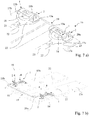
- Figure 7a reveals the opposite side of the printed circuit board 17b with an additional printed circuit board 17c of the printed circuit board arrangement 16 adjoining it.
- the printed circuit boards 17b, 17c lying next to one another on their longitudinal edge are now connected to one another in an electrically conductive manner.
- a wire bridge is again provided, which is designed as a non-curved, straight rod or electrical conductor.
- the free end sections 20a, 20b can be bent transversely to the plane without further bending of the wire bridge 19 the insulation displacement contact connections 2 are clamped to it.
- the printed circuit boards 17a, 17b, 17c carry electrical or electronic components 22, such as in particular light-emitting diodes.
- This circuit board arrangement 16 can thus be used for a lamp.
- the circuit boards 17a, 17b, 17c carry conductor tracks 23, which are soldered to the respective solder connection surfaces 13a, 13b with a respective conductor connection contact 1. Electrical energy can thus be supplied to the electrical / electronic components 22 to be supplied via the conductor connection contacts 1.
- Figure 7b shows a modified embodiment of a circuit board arrangement 16, in which the interconnected insulation displacement contact connections 2 are aligned such that the clamping slots 4 are not as in the exemplary embodiment according to FIG Figure 7a ) are aligned to each other. Therefore, the end sections 20a, 20b of the wire bridge 19 extend approximately parallel to one another in the same main direction of extension. The two end sections 20a, 20b are connected to one another by a cross bar 35.
- the wire bridge 19 is designed in the manner of a U-shaped element.
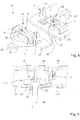
- Figure 8 shows a perspective detail view of the circuit board arrangement 16 in an area where electrical conductors 24 are each guided through a conductor lead-through opening 18 in the circuit board and the plug-in opening 10 of the conductor connection contact 1 lying above it.
- the free stripped end of an electrical conductor 24 is then clamped to the clamping edges of the spring-elastic clamping tongues 11 and contacted there in an electrically conductive manner and held mechanically firmly.
- a voltage potential can thus be applied to the printed circuit board arrangement 16 in order to supply the electrical / electronic components 22 with electrical power.
- the insulation displacement contact connections 2 are not assigned, as shown, when the electrical / electronic components 22 and their circuit boards 17a, 17b, 17c, 17d, 17e are connected in series.
- the insulation displacement contact connections 2 also carry a wire bridge 19 in order not only to transmit the electrical power via the conductor tracks 23 to the opposite conductor connection terminal 1 of the same printed circuit board 17a, 17b, 17c, 17d, 17e, but directly to an adjacent circuit board 17a, 17b, 17c, 17d, 17e.
- Figure 9 omits a sectional view of the circuit board arrangement 16 Figure 8 recognize with electrical conductor 24 clamped to it.
- the printed circuit board 17d is supported on a carrier element 25.
- This carrier element 25 can, for example, be a sheet metal housing of a lamp.
- a through opening 26 is introduced into the carrier element 25 in alignment with the conductor lead-through opening 18 of the printed circuit board 17 d and is closed with a lead-through seal 27.
- the electrical conductor 24 is then passed through the opening of the lead-through seal 27 in order to be contacted in an electrically conductive manner at a plug contact connection 8 as shown.
- a lens element 28 for example made of transparent plastic, is placed on the carrier element 25 in order to cover the lamp arrangement and to emit light emitted by the electronic components 22 in the form of light-emitting diodes as uniformly or as focused as possible.
- webs 29 of the lens element 28 in the region of the Protect insulation displacement contact connections 2. These webs 29 accommodate, for example, an insulation displacement contact connection 2 on both sides in a groove in a web 29.
- a slot is then present in the web 29 in the region of the intermediate space between the clamping fingers 3 in order to lead a wire bridge 19 through the web 29 and to clamp it on the assigned insulation displacement contact connection 2.
- the wire bridges 19 can be inserted into these webs 29, so that by placing the carrier element 25 with the preassembled printed circuit boards 17a, 17b, 17c, 17d on the lens element 28, the wire bridge 19 into the clamping slots 4 of the insulation displacement contact connections 2 are introduced.
- Figure 10 omits a perspective view of a section of a lamp arrangement 30 with the carrier element 25 Figure 9 and recognize strip-shaped printed circuit boards 17a, 17b, 17c, 17d installed therein. It becomes clear that each printed circuit board 17a, 17b, 17c, 17d carries conductor connection contacts 1 at their opposite ends adjacent to the narrow edges. These are arranged symmetrically with respect to one another, so that the insulation displacement contact connections 2 of such a pair of conductor connection contacts 1 each point to the other longitudinal edge or are arranged adjacent to the respective other longitudinal edge 31a, 31b.
- electrical conductors 24 are inserted from the underside of the carrier element 25 transversely to the plane of the printed circuit boards 17d, 17c in order to be clamped to the plug contact connections of these conductor connection contacts 1.
- the carrier element 25 is closed with an end cap 32, which is attached to the profile of the carrier element 25.
- Figure 11 shows a perspective view of a further embodiment of a conductor connection contact 1. This differs from the conductor connection contacts 1 described above in that there is no insulation displacement contact connection 2 for connecting an additional electrical conductor or a wire bridge. These conductor connection contacts 1 are provided, in particular, for the end connections of a lamp arrangement 30 to which energy supply / discharge lines are connected.
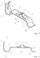
- Figure 12 reveals a modified embodiment of a conductor connection contact 1, in which the clamping tongues 11 are provided with a further bend 36 or a kink.
- the clamping tongues 11 are arranged at a greater angle to one another in their region which adjoins the connection surface 9 (ie at a flatter angle) than in the region adjoining the clamping edges 15.
- the section of the clamping tongues 11 adjoining the clamping edges 15 is thus steeper than the area of the clamping tongues 11 which merges into the connecting surface 9. This leads to a reduction in the insertion forces for the insertion of an electrical conductor and a loosening of a connected electrical conductor Conductor by turning and pulling is possible.
- This configuration of the clamping tongues 11 is in Figure 13 even clearer from the page display.
- the sections of the clamping tongues 11 adjoining the clamping edges 15 are arranged at an acute angle in the rest position without an inserted electrical conductor, while the sections of the clamping tongues 11 adjoining the connection surface 9 are aligned at an obtuse angle to one another are. This does not change even when an electrical conductor is clamped in, since both angles decrease due to the further raising of the clamping tongues 11, the relationship between obtuse angle and acute angle is still maintained.
- Figure 14 omits a perspective view of the modified embodiment Figures 12 and 13 detect.
- these bends 36 can also be made from other configurations of the conductor connection contacts 1, in particular the conductor connection contacts 1 Figure 1a ) and Figure 11 equally be provided.
- the clamping tongues are bent obliquely out of the connection surface 9 so that they point towards one another. Due to the bends 26 or a kink, the angle between the opposite sections of the clamping tongues 11 is reduced. As a result, the insertion forces for an electrical conductor inserted through the plug opening 10 are reduced and the conductor can be removed from the plug connection 8 by rotating and pulling.
- connection contact similar to that previously based on the Figure 11 explained conductor connection contact, a plug contact connection 8a in the connection surface 9.
- Two spring-elastic clamping tongues 11a are bent out of the material of the conductor connection contact 1, so that a plug opening 10a is formed there.
- the connection area 9 is also spaced apart from the plane of the solder connection areas 13a, 13b in that the ends of the conductor connection contact 1, which have the solder connection areas 13a, 13b, are connected to the connection area 9 via foot sections 14, which may run essentially vertically to the connection area 9, for example are.
- foot sections 14 in this embodiment can be somewhat extended compared to the embodiment of FIG Figure 11 be trained.
- a further plug contact connection 8b can, for example, be formed in one or in both foot sections 14.
- the Figures 15 and 16 each show only one further plug contact connection 8b in a foot section 14.
- the further plug contact connection 8b is formed by protruding a spring-elastic clamping tongue 11b from the material of the foot section 14, so that a plug opening 10b is formed there.
- the resilient clamping tongue 11b has a clamping edge. An electrical conductor can then be clamped between the underside of the connection surface 9 facing the clamping tongue 11b and this clamping edge.
- the plug contact connection 8a formed in the connection surface 9 has an insertion direction S which runs essentially perpendicular to the connection surface 9.
- the insertion direction S can, as in Figure 16 shown, run from bottom to top, or in the opposite direction if the spring-elastic clamping tongues 11a are bent out (downward) to the other side of the connection surface 9.
- the further plug contact connection 8b has a conductor insertion direction W which is essentially perpendicular to the conductor insertion direction S.
- an electrical conductor to be inserted can be inserted either horizontally (conductor insertion direction W) or vertically (conductor insertion direction S) to the connection surface 9 and accordingly to the circuit board parallel to it. If necessary, respective electrical conductors can also be plugged into both plug contact connections 8a, 8b.
- a conductor insertion tongue 110 is bent out in the opposite direction from the material of the conductor connection contact 1 on the opposite edge of the plug opening 10b, at which the spring-elastic clamping tongue 11b is not bent out, i.e. the conductor insertion tongue 110 points to the right in the opposite direction of the conductor insertion W.
- This forms a funnel-shaped conductor insertion which facilitates the insertion of an electrical conductor into the further plug contact connection 8b.
- the Figures 17 and 18 show a circuit board 17 with attached conductor connection contact according to the Figures 15 to 16 . It can be seen in particular in the Figure 18 the possibility of inserting an electrical conductor 24a vertically to the printed circuit board 17, and optionally or additionally an electrical conductor 24b horizontally to the printed circuit board 17.
- the conductor connection contact 1 projects according to the illustration in FIG Figures 17 and 18 through an opening in the printed circuit board 17 so that the overall height is reduced compared to the arrangement of the conductor connection contact 1 on the printed circuit board, as is shown, for example, in FIG Figure 8 is shown.
Landscapes
- Engineering & Computer Science (AREA)
- General Engineering & Computer Science (AREA)
- Coupling Device And Connection With Printed Circuit (AREA)
Applications Claiming Priority (4)
| Application Number | Priority Date | Filing Date | Title |
|---|---|---|---|
| DE102015120979 | 2015-12-02 | ||
| DE202016106235.7U DE202016106235U1 (de) | 2015-12-02 | 2016-11-08 | Leiteranschlusskontakt und Leiterplattenanordnung |
| EP16801757.2A EP3384561B1 (de) | 2015-12-02 | 2016-11-24 | Leiteranschlusskontakt und leiterplattenanordnung |
| PCT/EP2016/078689 WO2017093119A1 (de) | 2015-12-02 | 2016-11-24 | Leiteranschlusskontakt und leiterplattenanordnung |
Related Parent Applications (1)
| Application Number | Title | Priority Date | Filing Date |
|---|---|---|---|
| EP16801757.2A Division EP3384561B1 (de) | 2015-12-02 | 2016-11-24 | Leiteranschlusskontakt und leiterplattenanordnung |
Publications (1)
| Publication Number | Publication Date |
|---|---|
| EP3671960A1 true EP3671960A1 (de) | 2020-06-24 |
Family
ID=58405739
Family Applications (2)
| Application Number | Title | Priority Date | Filing Date |
|---|---|---|---|
| EP20157193.2A Withdrawn EP3671960A1 (de) | 2015-12-02 | 2016-11-24 | Leiteranschlusskontakt und leiterplattenanordnung |
| EP16801757.2A Active EP3384561B1 (de) | 2015-12-02 | 2016-11-24 | Leiteranschlusskontakt und leiterplattenanordnung |
Family Applications After (1)
| Application Number | Title | Priority Date | Filing Date |
|---|---|---|---|
| EP16801757.2A Active EP3384561B1 (de) | 2015-12-02 | 2016-11-24 | Leiteranschlusskontakt und leiterplattenanordnung |
Country Status (5)
| Country | Link |
|---|---|
| EP (2) | EP3671960A1 (pl) |
| CN (3) | CN111509413B (pl) |
| DE (2) | DE202016106235U1 (pl) |
| PL (1) | PL3384561T3 (pl) |
| WO (1) | WO2017093119A1 (pl) |
Families Citing this family (8)
| Publication number | Priority date | Publication date | Assignee | Title |
|---|---|---|---|---|
| AT519780B1 (de) * | 2017-03-20 | 2020-02-15 | Zkw Group Gmbh | Verfahren zum Herstellen von Bondverbindungen |
| FR3084972B1 (fr) * | 2018-08-13 | 2021-12-10 | Valeo Siemens Eautomotive France Sas | Ensemble electrique |
| CN109681823B (zh) * | 2018-11-16 | 2024-05-28 | 上海悟城智能系统集成有限公司 | 背插式一体型led模块化路灯 |
| DE102019207582A1 (de) * | 2019-05-23 | 2020-11-26 | Siemens Schweiz Ag | SMD-fähige THT-Aufnahme |
| AU2021292753B2 (en) | 2020-06-18 | 2023-12-21 | Ideal Industries, Inc. | Conductor terminal |
| DE102022211669A1 (de) * | 2022-11-04 | 2024-05-08 | Robert Bosch Gesellschaft mit beschränkter Haftung | Steuergerät, Antriebseinheit mit einem Steuergerät und Verfahren zur Herstellung einer Antriebseinheit |
| DE102024201384B3 (de) | 2024-02-15 | 2025-06-12 | Robert Bosch Gesellschaft mit beschränkter Haftung | Leiterplatte mit zumindest einem Kontaktelement, Gehäuse mit einer solchen Leiterplatte und Verfahren zum Herstellen einer niederohmigen elektrischen Verbindung |
| DE102024117834A1 (de) | 2024-06-25 | 2024-09-05 | Bayerische Motoren Werke Aktiengesellschaft | Stecker zum Einzeladerabgriff für ein eine Mehrzahl von Adern aufweisendes Flachbandkabel einer Energiespeichervorrichtung eines Kraftfahrzeugs, Flachbandkabelanordnung, Energiespeichervorrichtung, Kraftfahrzeug |
Citations (9)
| Publication number | Priority date | Publication date | Assignee | Title |
|---|---|---|---|---|
| EP0043165A1 (en) | 1980-06-26 | 1982-01-06 | E.I. Du Pont De Nemours And Company | Box connector |
| DE4412300C1 (de) * | 1994-04-09 | 1995-05-24 | Broekelmann Jaeger & Busse | Elektrischer Kontakt zum Anschluß von mindestens zwei Leitern |
| DE19512221A1 (de) | 1995-03-22 | 1996-09-26 | Wago Verwaltungs Gmbh | Elektr. Klemmenleiste für Leiterplatten |
| DE19617259A1 (de) | 1996-04-18 | 1997-10-23 | Wago Verwaltungs Gmbh | Elektr. Klemme mit einem nach oben offenen Schneidklemmkontakt |
| DE20001510U1 (de) | 2000-01-27 | 2001-06-13 | Weidmüller Interface GmbH & Co, 32760 Detmold | Anschlußvorrichtung für elektrische Leiter mit Schneidkontaktelementen |
| DE102006052119A1 (de) | 2006-11-06 | 2008-05-08 | Robert Bosch Gmbh | Schneid-Klemm-Verbindung, sowie Verfahren zur Verbindung zweier Bauteile |
| DE202014101012U1 (de) * | 2014-03-07 | 2015-06-11 | Zumtobel Lighting Gmbh | Elektrische Verbindungsmittel zum Anschließen eines elektrischen Verbrauchers an eine elektrische Leiterbahn, sowie System mit elektrischen Einheiten |
| CN204632931U (zh) * | 2015-04-02 | 2015-09-09 | 厦门广泓工贸有限公司 | 一种头箍型金属母端连接器及其应用的led灯 |
| DE212014000059U1 (de) * | 2014-03-19 | 2015-11-03 | Bingshui Chen | Kronenförmiger Verbinder und Leuchtdiodenlampe mit diesem kronenförmigen Verbinder |
Family Cites Families (1)
| Publication number | Priority date | Publication date | Assignee | Title |
|---|---|---|---|---|
| CN103367963A (zh) * | 2012-03-29 | 2013-10-23 | 朴振雨 | 接触器 |
-
2016
- 2016-11-08 DE DE202016106235.7U patent/DE202016106235U1/de active Active
- 2016-11-24 WO PCT/EP2016/078689 patent/WO2017093119A1/de not_active Ceased
- 2016-11-24 EP EP20157193.2A patent/EP3671960A1/de not_active Withdrawn
- 2016-11-24 CN CN201911409795.0A patent/CN111509413B/zh active Active
- 2016-11-24 DE DE202016008612.0U patent/DE202016008612U1/de active Active
- 2016-11-24 EP EP16801757.2A patent/EP3384561B1/de active Active
- 2016-11-24 PL PL16801757T patent/PL3384561T3/pl unknown
- 2016-11-24 CN CN201680070413.4A patent/CN108292810B/zh active Active
- 2016-11-24 CN CN201911417669.XA patent/CN111509414B/zh active Active
Patent Citations (9)
| Publication number | Priority date | Publication date | Assignee | Title |
|---|---|---|---|---|
| EP0043165A1 (en) | 1980-06-26 | 1982-01-06 | E.I. Du Pont De Nemours And Company | Box connector |
| DE4412300C1 (de) * | 1994-04-09 | 1995-05-24 | Broekelmann Jaeger & Busse | Elektrischer Kontakt zum Anschluß von mindestens zwei Leitern |
| DE19512221A1 (de) | 1995-03-22 | 1996-09-26 | Wago Verwaltungs Gmbh | Elektr. Klemmenleiste für Leiterplatten |
| DE19617259A1 (de) | 1996-04-18 | 1997-10-23 | Wago Verwaltungs Gmbh | Elektr. Klemme mit einem nach oben offenen Schneidklemmkontakt |
| DE20001510U1 (de) | 2000-01-27 | 2001-06-13 | Weidmüller Interface GmbH & Co, 32760 Detmold | Anschlußvorrichtung für elektrische Leiter mit Schneidkontaktelementen |
| DE102006052119A1 (de) | 2006-11-06 | 2008-05-08 | Robert Bosch Gmbh | Schneid-Klemm-Verbindung, sowie Verfahren zur Verbindung zweier Bauteile |
| DE202014101012U1 (de) * | 2014-03-07 | 2015-06-11 | Zumtobel Lighting Gmbh | Elektrische Verbindungsmittel zum Anschließen eines elektrischen Verbrauchers an eine elektrische Leiterbahn, sowie System mit elektrischen Einheiten |
| DE212014000059U1 (de) * | 2014-03-19 | 2015-11-03 | Bingshui Chen | Kronenförmiger Verbinder und Leuchtdiodenlampe mit diesem kronenförmigen Verbinder |
| CN204632931U (zh) * | 2015-04-02 | 2015-09-09 | 厦门广泓工贸有限公司 | 一种头箍型金属母端连接器及其应用的led灯 |
Also Published As
| Publication number | Publication date |
|---|---|
| DE202016106235U1 (de) | 2017-03-03 |
| PL3384561T3 (pl) | 2020-07-27 |
| CN111509413B (zh) | 2022-03-15 |
| EP3384561B1 (de) | 2020-02-26 |
| CN111509414A (zh) | 2020-08-07 |
| DE202016008612U1 (de) | 2018-08-22 |
| CN111509414B (zh) | 2021-11-19 |
| CN108292810A (zh) | 2018-07-17 |
| CN108292810B (zh) | 2020-02-04 |
| WO2017093119A1 (de) | 2017-06-08 |
| CN111509413A (zh) | 2020-08-07 |
| EP3384561A1 (de) | 2018-10-10 |
Similar Documents
| Publication | Publication Date | Title |
|---|---|---|
| EP3384561B1 (de) | Leiteranschlusskontakt und leiterplattenanordnung | |
| EP2092813B1 (de) | Elektrische leiterplatte mit einer anschlussklemme | |
| DE102006028814A1 (de) | Kontaktelement zum Anschließen eines elektrischen Leiters | |
| EP3375048B1 (de) | Steckkontakt | |
| EP3114734B1 (de) | Anschluss- oder verbindungsklemme | |
| EP0800233A1 (de) | Kontaktfeder, insbesondere für einen elektrischen Steckverbinder | |
| EP2608322A1 (de) | Leiteranschlussklemme | |
| DE102017124594A1 (de) | Vorrichtung zur elektrischen Kontaktierung | |
| DE202006000380U1 (de) | Leiterplatte mit einem Verbindungselement | |
| DE102012016281A1 (de) | Elektrische Verbindungsanordnung und deren Bauteile | |
| DE19731411A1 (de) | Haltevorrichtung für elektrische Lüfter, insbesondere Kleinstlüfter | |
| DE102014114352B3 (de) | Stiftleiste | |
| DE102010043495B4 (de) | Elektrisches Bauteil zur Oberflächenmontage | |
| DE4406200C1 (de) | Stiftförmiges Kontaktelement | |
| DE202013104811U1 (de) | Elektrische Kontaktvorrichtung, insbesondere elektrische Printklemme und/oder Grundleiste | |
| DE102015120980B4 (de) | Leiterplattenanordnung und Leuchtenanordnung | |
| DE19611422C2 (de) | Verbinder für die elektrische Verbindung von zwei Leiterplatten miteinander | |
| DE102012105995B4 (de) | Oberflächenmontierbare elektrische Einrichtung | |
| DE102004031949B4 (de) | Elektrischer Steckverbinder | |
| DE19614988A1 (de) | Elektrische Anschlußvorrichtung und elektrisches Verbindungselement zur Verwendung in einer elektrischen Anschlußvorrichtung | |
| DE102008046567B3 (de) | Steckverbinder zum Anschließen eines elektrischen Leiters an eine Leiterplatte | |
| DE102013003389B4 (de) | Baugruppe bestehend aus mindestens zwei benachbart zueinander angeordneten elektrischen Anschlussklemmen und einem Querverbinder | |
| WO2002073746A1 (de) | Leitungsverbinder | |
| DE102024123164A1 (de) | Leiteranschlussklemmen-Anordnung und Brückerelement dafür | |
| EP1168510B1 (de) | Elektrische Verbindungsvorrichtung |
Legal Events
| Date | Code | Title | Description |
|---|---|---|---|
| PUAI | Public reference made under article 153(3) epc to a published international application that has entered the european phase |
Free format text: ORIGINAL CODE: 0009012 |
|
| STAA | Information on the status of an ep patent application or granted ep patent |
Free format text: STATUS: REQUEST FOR EXAMINATION WAS MADE |
|
| 17P | Request for examination filed |
Effective date: 20200213 |
|
| AC | Divisional application: reference to earlier application |
Ref document number: 3384561 Country of ref document: EP Kind code of ref document: P |
|
| AK | Designated contracting states |
Kind code of ref document: A1 Designated state(s): AL AT BE BG CH CY CZ DE DK EE ES FI FR GB GR HR HU IE IS IT LI LT LU LV MC MK MT NL NO PL PT RO RS SE SI SK SM TR |
|
| GRAP | Despatch of communication of intention to grant a patent |
Free format text: ORIGINAL CODE: EPIDOSNIGR1 |
|
| STAA | Information on the status of an ep patent application or granted ep patent |
Free format text: STATUS: GRANT OF PATENT IS INTENDED |
|
| RIC1 | Information provided on ipc code assigned before grant |
Ipc: H01R 12/70 20110101ALI20200729BHEP Ipc: H01R 12/57 20110101ALI20200729BHEP Ipc: H01R 4/50 20060101ALI20200729BHEP Ipc: H01R 12/53 20110101ALI20200729BHEP Ipc: H01R 4/48 20060101ALI20200729BHEP Ipc: F21V 23/06 20060101ALN20200729BHEP Ipc: H01R 12/72 20110101ALN20200729BHEP Ipc: H01R 12/73 20110101ALN20200729BHEP Ipc: H01R 4/2425 20180101AFI20200729BHEP |
|
| RIC1 | Information provided on ipc code assigned before grant |
Ipc: H01R 12/57 20110101ALI20200804BHEP Ipc: H01R 4/50 20060101ALI20200804BHEP Ipc: H01R 12/72 20110101ALN20200804BHEP Ipc: H01R 4/2425 20180101AFI20200804BHEP Ipc: H01R 12/70 20110101ALI20200804BHEP Ipc: F21V 23/06 20060101ALN20200804BHEP Ipc: H01R 12/73 20110101ALN20200804BHEP Ipc: H01R 12/53 20110101ALI20200804BHEP Ipc: H01R 4/48 20060101ALI20200804BHEP |
|
| INTG | Intention to grant announced |
Effective date: 20200818 |
|
| GRAJ | Information related to disapproval of communication of intention to grant by the applicant or resumption of examination proceedings by the epo deleted |
Free format text: ORIGINAL CODE: EPIDOSDIGR1 |
|
| STAA | Information on the status of an ep patent application or granted ep patent |
Free format text: STATUS: REQUEST FOR EXAMINATION WAS MADE |
|
| GRAS | Grant fee paid |
Free format text: ORIGINAL CODE: EPIDOSNIGR3 |
|
| STAA | Information on the status of an ep patent application or granted ep patent |
Free format text: STATUS: GRANT OF PATENT IS INTENDED |
|
| GRAP | Despatch of communication of intention to grant a patent |
Free format text: ORIGINAL CODE: EPIDOSNIGR1 |
|
| INTC | Intention to grant announced (deleted) | ||
| RIC1 | Information provided on ipc code assigned before grant |
Ipc: H01R 4/48 20060101ALI20201116BHEP Ipc: F21V 23/06 20060101ALN20201116BHEP Ipc: H01R 12/53 20110101ALI20201116BHEP Ipc: H01R 12/72 20110101ALN20201116BHEP Ipc: H01R 4/50 20060101ALI20201116BHEP Ipc: H01R 12/70 20110101ALI20201116BHEP Ipc: H01R 4/2425 20180101AFI20201116BHEP Ipc: H01R 12/57 20110101ALI20201116BHEP Ipc: H01R 12/73 20110101ALN20201116BHEP |
|
| INTG | Intention to grant announced |
Effective date: 20201130 |
|
| STAA | Information on the status of an ep patent application or granted ep patent |
Free format text: STATUS: THE APPLICATION IS DEEMED TO BE WITHDRAWN |
|
| 18D | Application deemed to be withdrawn |
Effective date: 20210413 |