EP3671960A1 - Wire connection contact and circuit board assembly - Google Patents
Wire connection contact and circuit board assembly Download PDFInfo
- Publication number
- EP3671960A1 EP3671960A1 EP20157193.2A EP20157193A EP3671960A1 EP 3671960 A1 EP3671960 A1 EP 3671960A1 EP 20157193 A EP20157193 A EP 20157193A EP 3671960 A1 EP3671960 A1 EP 3671960A1
- Authority
- EP
- European Patent Office
- Prior art keywords
- connection
- contact
- conductor
- circuit board
- printed circuit
- Prior art date
- Legal status (The legal status is an assumption and is not a legal conclusion. Google has not performed a legal analysis and makes no representation as to the accuracy of the status listed.)
- Withdrawn
Links
- 239000004020 conductor Substances 0.000 claims abstract description 192
- 229910000679 solder Inorganic materials 0.000 claims abstract description 50
- 238000009413 insulation Methods 0.000 claims description 70
- 238000006073 displacement reaction Methods 0.000 claims description 69
- 238000003780 insertion Methods 0.000 claims description 35
- 230000037431 insertion Effects 0.000 claims description 35
- 239000000463 material Substances 0.000 claims description 16
- 238000005476 soldering Methods 0.000 claims description 5
- 210000002105 tongue Anatomy 0.000 description 44
- 230000001154 acute effect Effects 0.000 description 3
- 239000002184 metal Substances 0.000 description 3
- 238000010276 construction Methods 0.000 description 2
- 230000007423 decrease Effects 0.000 description 2
- 239000007769 metal material Substances 0.000 description 2
- 238000005452 bending Methods 0.000 description 1
- 230000005484 gravity Effects 0.000 description 1
- 239000011159 matrix material Substances 0.000 description 1
- 229920003023 plastic Polymers 0.000 description 1
- 230000007704 transition Effects 0.000 description 1
- 238000011144 upstream manufacturing Methods 0.000 description 1
Images


Classifications
-
- H—ELECTRICITY
- H01—ELECTRIC ELEMENTS
- H01R—ELECTRICALLY-CONDUCTIVE CONNECTIONS; STRUCTURAL ASSOCIATIONS OF A PLURALITY OF MUTUALLY-INSULATED ELECTRICAL CONNECTING ELEMENTS; COUPLING DEVICES; CURRENT COLLECTORS
- H01R4/00—Electrically-conductive connections between two or more conductive members in direct contact, i.e. touching one another; Means for effecting or maintaining such contact; Electrically-conductive connections having two or more spaced connecting locations for conductors and using contact members penetrating insulation
- H01R4/28—Clamped connections, spring connections
- H01R4/48—Clamped connections, spring connections utilising a spring, clip, or other resilient member
- H01R4/4809—Clamped connections, spring connections utilising a spring, clip, or other resilient member using a leaf spring to bias the conductor toward the busbar
- H01R4/48185—Clamped connections, spring connections utilising a spring, clip, or other resilient member using a leaf spring to bias the conductor toward the busbar adapted for axial insertion of a wire end
-
- F—MECHANICAL ENGINEERING; LIGHTING; HEATING; WEAPONS; BLASTING
- F21—LIGHTING
- F21V—FUNCTIONAL FEATURES OR DETAILS OF LIGHTING DEVICES OR SYSTEMS THEREOF; STRUCTURAL COMBINATIONS OF LIGHTING DEVICES WITH OTHER ARTICLES, NOT OTHERWISE PROVIDED FOR
- F21V23/00—Arrangement of electric circuit elements in or on lighting devices
- F21V23/06—Arrangement of electric circuit elements in or on lighting devices the elements being coupling devices, e.g. connectors
-
- H—ELECTRICITY
- H01—ELECTRIC ELEMENTS
- H01R—ELECTRICALLY-CONDUCTIVE CONNECTIONS; STRUCTURAL ASSOCIATIONS OF A PLURALITY OF MUTUALLY-INSULATED ELECTRICAL CONNECTING ELEMENTS; COUPLING DEVICES; CURRENT COLLECTORS
- H01R12/00—Structural associations of a plurality of mutually-insulated electrical connecting elements, specially adapted for printed circuits, e.g. printed circuit boards [PCB], flat or ribbon cables, or like generally planar structures, e.g. terminal strips, terminal blocks; Coupling devices specially adapted for printed circuits, flat or ribbon cables, or like generally planar structures; Terminals specially adapted for contact with, or insertion into, printed circuits, flat or ribbon cables, or like generally planar structures
- H01R12/50—Fixed connections
- H01R12/51—Fixed connections for rigid printed circuits or like structures
- H01R12/53—Fixed connections for rigid printed circuits or like structures connecting to cables except for flat or ribbon cables
-
- H—ELECTRICITY
- H01—ELECTRIC ELEMENTS
- H01R—ELECTRICALLY-CONDUCTIVE CONNECTIONS; STRUCTURAL ASSOCIATIONS OF A PLURALITY OF MUTUALLY-INSULATED ELECTRICAL CONNECTING ELEMENTS; COUPLING DEVICES; CURRENT COLLECTORS
- H01R12/00—Structural associations of a plurality of mutually-insulated electrical connecting elements, specially adapted for printed circuits, e.g. printed circuit boards [PCB], flat or ribbon cables, or like generally planar structures, e.g. terminal strips, terminal blocks; Coupling devices specially adapted for printed circuits, flat or ribbon cables, or like generally planar structures; Terminals specially adapted for contact with, or insertion into, printed circuits, flat or ribbon cables, or like generally planar structures
- H01R12/50—Fixed connections
- H01R12/51—Fixed connections for rigid printed circuits or like structures
- H01R12/55—Fixed connections for rigid printed circuits or like structures characterised by the terminals
- H01R12/57—Fixed connections for rigid printed circuits or like structures characterised by the terminals surface mounting terminals
-
- H—ELECTRICITY
- H01—ELECTRIC ELEMENTS
- H01R—ELECTRICALLY-CONDUCTIVE CONNECTIONS; STRUCTURAL ASSOCIATIONS OF A PLURALITY OF MUTUALLY-INSULATED ELECTRICAL CONNECTING ELEMENTS; COUPLING DEVICES; CURRENT COLLECTORS
- H01R12/00—Structural associations of a plurality of mutually-insulated electrical connecting elements, specially adapted for printed circuits, e.g. printed circuit boards [PCB], flat or ribbon cables, or like generally planar structures, e.g. terminal strips, terminal blocks; Coupling devices specially adapted for printed circuits, flat or ribbon cables, or like generally planar structures; Terminals specially adapted for contact with, or insertion into, printed circuits, flat or ribbon cables, or like generally planar structures
- H01R12/70—Coupling devices
- H01R12/7005—Guiding, mounting, polarizing or locking means; Extractors
- H01R12/7011—Locking or fixing a connector to a PCB
- H01R12/707—Soldering or welding
-
- H—ELECTRICITY
- H01—ELECTRIC ELEMENTS
- H01R—ELECTRICALLY-CONDUCTIVE CONNECTIONS; STRUCTURAL ASSOCIATIONS OF A PLURALITY OF MUTUALLY-INSULATED ELECTRICAL CONNECTING ELEMENTS; COUPLING DEVICES; CURRENT COLLECTORS
- H01R12/00—Structural associations of a plurality of mutually-insulated electrical connecting elements, specially adapted for printed circuits, e.g. printed circuit boards [PCB], flat or ribbon cables, or like generally planar structures, e.g. terminal strips, terminal blocks; Coupling devices specially adapted for printed circuits, flat or ribbon cables, or like generally planar structures; Terminals specially adapted for contact with, or insertion into, printed circuits, flat or ribbon cables, or like generally planar structures
- H01R12/70—Coupling devices
- H01R12/71—Coupling devices for rigid printing circuits or like structures
- H01R12/72—Coupling devices for rigid printing circuits or like structures coupling with the edge of the rigid printed circuits or like structures
- H01R12/722—Coupling devices for rigid printing circuits or like structures coupling with the edge of the rigid printed circuits or like structures coupling devices mounted on the edge of the printed circuits
- H01R12/728—Coupling devices without an insulating housing provided on the edge of the PCB
-
- H—ELECTRICITY
- H01—ELECTRIC ELEMENTS
- H01R—ELECTRICALLY-CONDUCTIVE CONNECTIONS; STRUCTURAL ASSOCIATIONS OF A PLURALITY OF MUTUALLY-INSULATED ELECTRICAL CONNECTING ELEMENTS; COUPLING DEVICES; CURRENT COLLECTORS
- H01R12/00—Structural associations of a plurality of mutually-insulated electrical connecting elements, specially adapted for printed circuits, e.g. printed circuit boards [PCB], flat or ribbon cables, or like generally planar structures, e.g. terminal strips, terminal blocks; Coupling devices specially adapted for printed circuits, flat or ribbon cables, or like generally planar structures; Terminals specially adapted for contact with, or insertion into, printed circuits, flat or ribbon cables, or like generally planar structures
- H01R12/70—Coupling devices
- H01R12/71—Coupling devices for rigid printing circuits or like structures
- H01R12/72—Coupling devices for rigid printing circuits or like structures coupling with the edge of the rigid printed circuits or like structures
- H01R12/73—Coupling devices for rigid printing circuits or like structures coupling with the edge of the rigid printed circuits or like structures connecting to other rigid printed circuits or like structures
- H01R12/732—Printed circuits being in the same plane
-
- H—ELECTRICITY
- H01—ELECTRIC ELEMENTS
- H01R—ELECTRICALLY-CONDUCTIVE CONNECTIONS; STRUCTURAL ASSOCIATIONS OF A PLURALITY OF MUTUALLY-INSULATED ELECTRICAL CONNECTING ELEMENTS; COUPLING DEVICES; CURRENT COLLECTORS
- H01R4/00—Electrically-conductive connections between two or more conductive members in direct contact, i.e. touching one another; Means for effecting or maintaining such contact; Electrically-conductive connections having two or more spaced connecting locations for conductors and using contact members penetrating insulation
- H01R4/02—Soldered or welded connections
- H01R4/023—Soldered or welded connections between cables or wires and terminals
-
- H—ELECTRICITY
- H01—ELECTRIC ELEMENTS
- H01R—ELECTRICALLY-CONDUCTIVE CONNECTIONS; STRUCTURAL ASSOCIATIONS OF A PLURALITY OF MUTUALLY-INSULATED ELECTRICAL CONNECTING ELEMENTS; COUPLING DEVICES; CURRENT COLLECTORS
- H01R4/00—Electrically-conductive connections between two or more conductive members in direct contact, i.e. touching one another; Means for effecting or maintaining such contact; Electrically-conductive connections having two or more spaced connecting locations for conductors and using contact members penetrating insulation
- H01R4/24—Connections using contact members penetrating or cutting insulation or cable strands
- H01R4/2416—Connections using contact members penetrating or cutting insulation or cable strands the contact members having insulation-cutting edges, e.g. of tuning fork type
- H01R4/242—Connections using contact members penetrating or cutting insulation or cable strands the contact members having insulation-cutting edges, e.g. of tuning fork type the contact members being plates having a single slot
- H01R4/2425—Flat plates, e.g. multi-layered flat plates
-
- H—ELECTRICITY
- H01—ELECTRIC ELEMENTS
- H01R—ELECTRICALLY-CONDUCTIVE CONNECTIONS; STRUCTURAL ASSOCIATIONS OF A PLURALITY OF MUTUALLY-INSULATED ELECTRICAL CONNECTING ELEMENTS; COUPLING DEVICES; CURRENT COLLECTORS
- H01R4/00—Electrically-conductive connections between two or more conductive members in direct contact, i.e. touching one another; Means for effecting or maintaining such contact; Electrically-conductive connections having two or more spaced connecting locations for conductors and using contact members penetrating insulation
- H01R4/28—Clamped connections, spring connections
- H01R4/48—Clamped connections, spring connections utilising a spring, clip, or other resilient member
-
- H—ELECTRICITY
- H01—ELECTRIC ELEMENTS
- H01R—ELECTRICALLY-CONDUCTIVE CONNECTIONS; STRUCTURAL ASSOCIATIONS OF A PLURALITY OF MUTUALLY-INSULATED ELECTRICAL CONNECTING ELEMENTS; COUPLING DEVICES; CURRENT COLLECTORS
- H01R4/00—Electrically-conductive connections between two or more conductive members in direct contact, i.e. touching one another; Means for effecting or maintaining such contact; Electrically-conductive connections having two or more spaced connecting locations for conductors and using contact members penetrating insulation
- H01R4/28—Clamped connections, spring connections
- H01R4/50—Clamped connections, spring connections utilising a cam, wedge, cone or ball also combined with a screw
- H01R4/5083—Clamped connections, spring connections utilising a cam, wedge, cone or ball also combined with a screw using a wedge
Definitions
- the invention relates to a conductor connection contact with a solder connection surface for connection to a printed circuit board and a plug contact connection with a spring clamp element.
- the invention further relates to a circuit board arrangement with a circuit board, a conductor connection contact being soldered to the circuit board with its soldering areas.
- Printed circuit boards with electrical / electronic components mounted on them have conductor connection contacts for the electrically conductive connection of conductors or for connecting adjacent printed circuit boards to one another. These are soldered onto the PCB in a push-through or surface mounting and connected to it electrically and mechanically.
- DE 200 01 510 U1 shows a connection device for electrical conductors with insulation displacement contact connections soldered onto a circuit board.
- a contact element is designed as a sheet metal stamped / bent part and has two mutually parallel pairs of contact cutting edges that widen in the manner of an opening in their end region to cut open the insulation of an electrical conductor to be clamped on.
- the contact blades of each pair of contact blades are separated from one another by slots.
- the two pairs of contact blades are connected to one another via lateral webs.
- Several such cutting contact elements are connected to one another in a band-like manner for assembly on the printed circuit board.
- EP 0 043 165 A1 shows an insulation displacement contact with two conductor connection areas aligned transversely to one another.
- the conductor connection areas are each formed by clamping slots on opposite walls, the walls being folded over into a box.
- DE 10 2006 052 119 A1 discloses an insulation displacement connection with a first insulation displacement element attached to a first component and a second insulation displacement element attached to a second component.
- the two insulation displacement elements can be pushed into one another in the joining direction and can be displaced relative to one another transversely to the joining direction.
- DE 196 17 259 A1 discloses an electrical terminal with an upwardly open insulation displacement contact and further plug contacts which are arranged in the lower part of the terminal.
- the clamp is made in one piece from a band-shaped metal strip, one end piece of the strip material being divided into several tongues, one of which, as an anchor end piece, stabilizes the shape of the clamp and the other, as leaf spring end pieces, form the insulation displacement contacts .
- Printed circuit board solder pins protrude from a bottom surface which connects the insulation displacement contact and the leaf spring end piece.
- DE 195 12 221 A1 shows an electrical terminal block for printed circuit boards with a bridging rail which can be plugged onto solder connection pins.
- the bridging rail is designed as an essentially planar, flat bridging band which has push-through slots which are formed by two resilient tongues punched out of the bridging band.
- connection surface has a plug opening and at least one spring-elastic clamping tongue to form the spring clamping element. This enables the simple connection of an electrical conductor which is inserted through the plug-in opening and clamped to the connection surface of the plug-in contact connection by means of the spring-elastic clamping tongue.
- connection area then merges into a foot region, which is in each case connected to a solder connection area or has a solder connection area on its side facing away from the connection area.
- connection area is stably supported at a distance from the plane of the printed circuit board with the aid of the foot regions.
- the solder connection areas adjoining the foot areas ensure that the plug contact connection is kept stable on the solder connection areas when the solder connection contact is soldered to a printed circuit board.
- the current flow then goes through the foot areas directly to the solder connection surface, so that the current-conducting cross-sections and paths are optimized.
- resilient clamping tongues can be bent out to point towards each other.
- the freely movable ends of the clamping tongues then form clamping edges for clamping an electrical conductor or contact pin inserted into the insertion opening.
- An electrical conductor or contact pin can thus be connected very reliably with an extremely simple construction of the conductor connection contact.
- the current paths then lead the shortest way over the clamping tongues and the foot sections to the solder connection areas.
- An insulation displacement contact connection can also be present on the conductor connection contact.
- a solder connection surface can be arranged between an insulation displacement contact connection and a web leading to the connection level. This has the advantage that the insulation displacement contact connection and the connection surface are connected to one another via the common solder connection surface, the current paths between insulation displacement connection contact terminal and plug contact connection being short and the insulation displacement contact connection and the plug contact connection via the common solder connection surface are mechanically stabilized.
- the insulation displacement contact connection can have two spaced-apart contact fingers which are connected to one another in a common root section.
- the root section then merges into the foot section or forms the foot section. It is conceivable that the root section merges into one of the solder connection surfaces. This then leads to a very compact structure of the solder connection contact.
- the direction of extension of a wire bridge clamped to the insulation displacement contact connection in the clamping region on the insulation displacement contact connection can be oriented transversely to the direction of insertion of the plug contact connection.
- the direction of extension of the wire bridge at the insulation displacement contact connection in the region of the clamping point, in which a wire bridge is guided to the clamping point between the contact fingers, runs in the plugging direction of the plug contact connection.
- the plane spanned by contact fingers of the cutting plug contact connection or a slotted wall to form the cutting plug contact connection is thus oriented transversely to the plane of the connection surface.
- Transversal means an orientation in the angular range of 90 ° +/- 20 ° and preferably 90 ° +/- 5 °.
- the direction of extension of the wire bridge clamped to the insulation displacement contact connection in the clamping region of this insulation displacement contact connection can be in the direction of extension of the connection surface or also transverse to the direction of extension of the connection surface. However, it is also conceivable that it is oriented obliquely to the direction of extension of the connection surface.
- the circuit board arrangement has a circuit board in which such a conductor connection contact is soldered onto the circuit board with its soldering areas. The circuit board then has a conductor lead-through opening below the plug-in opening, so that an electrical conductor can be inserted through the conductor lead-through opening into the plug-in opening and clamped on the plug contact connection. This enables a very compact connection of an electrical conductor to the circuit board with a plug-in direction perpendicular to the circuit board.
- connection area of the conductor connection contact can extend parallel to the plane of the circuit board. A section of the conductor connection contact having the insulation displacement contact connection then protrudes from the plane of the circuit board.
- a material flap can be spaced from the connection surface to one of the solder connection surfaces, e.g. protrude in the direction of an insulation displacement contact connection.
- the connection area adjacent to the plug contact connection is thus enlarged.
- This material flap also known as a flap
- the clamping spring tongues can have a kink or a bend in an area upstream of the respective clamping edge.
- the clamping tongues bent out toward one another are oriented at a greater angle to one another in the regions adjacent to the connection surface than in the region adjacent to the clamping edge. Due to the kink or the bend, the surfaces of the opposing clamping tongues adjoining the clamping edges are thus arranged at an acute angle to one another.
- the direction of insertion for inserting an electrical conductor into the plug contact connection is substantially perpendicular to the spatial extent of at least one of the solder connection surfaces. In this way, the electrical conductor can be conveniently inserted into the plug contact connection transversely to the spatial extent of the printed circuit board from the top or the bottom.
- a resilient clamping tongue is arranged on an edge of the plug-in opening and a conductor insertion tongue is arranged on an edge of the plug-in opening opposite this edge, the clamping tongue and the conductor insertion tongue being bent away from each other.
- the conductor insertion tongue can form a conductor insertion slope for the simplified insertion of an electrical conductor to a clamping point formed with a freely movable end of the clamping tongue.
- the conductor insertion tongue is not necessarily part of the clamping point itself or does not necessarily have to form a counter bearing when the electrical conductor is clamped by the clamping tongue.
- the counter bearing can e.g. be formed by the connection surface of the conductor connection contact.
- the conductor connection contact has a further plug contact connection, the insertion direction of which for inserting a conductor into the further plug connection is essentially orthogonal to an insertion direction of the plug contact connection formed on the connection surface.
- the further plug contact connection can e.g. be formed on a foot section of the conductor connection contact.
- the conductor connection contact can also have a plurality of further plug contact connections with the mentioned orthogonal insertion direction, e.g. one or more such plug contact connections in each of the foot sections. In this way e.g. looping through an electrical potential can be realized from one circuit board to the next circuit board.
- circuit boards By combining a vertical and a horizontal conductor connection on one and the same conductor connection contact, e.g. an SMD terminal, circuit boards can be wired both vertically (from the back of the circuit board) and horizontally (on the top of the circuit board). This means that no circuit boards for the respective application need to be manufactured with specially shaped conductor connection contacts. Instead, a circuit board can be manufactured and used for both types of wiring. For example, luminaire manufacturers can use a single LED module with such a conductor connection contact for luminaires wired on the front and rear.
- the insertion direction of the first-mentioned plug contact connection which is formed on the connection surface of the conductor connection contact, can optionally point towards the front or the back of the circuit board, i.e. from the side of the conductor connection contact on which the foot sections protrude from the connection area, or from the opposite side of the connection area. Wiring can thus also be made possible for both contacting directions on the top side of the printed circuit board.
- the further plug contact connection can permit wiring on the top side of the printed circuit board or on the underside of the printed circuit board, depending on which side the solder connection surface is formed on.
- the conductor connection contact can also be provided with solder connection surfaces on both sides be formed so that either the conductor connection contact protrudes from one side of the circuit board and is not passed through an opening in the circuit board, or is passed through an opening in the circuit board and protrudes on the opposite side of the circuit board.
- the circuit board arrangement can have a plurality of circuit boards which are arranged adjacent to one another.
- the conductor connection contacts are then arranged diagonally offset from one another on opposite edge regions of the printed circuit board.
- the adjacent circuit boards can thus be connected to one another in an electrically conductive manner by means of wire bridges, which extend between the conductor connection contacts lying opposite one another.
- the diagonally offset arrangement of the conductor connection contacts then leads the wire bridges over several bends, so that sufficient tolerance compensation for thermal expansion is ensured. Due to the diagonally offset arrangement of the conductor connection contacts, a point or mirror symmetrical arrangement of the conductor connection contacts on a circuit board is also possible. For example, conductor terminal contacts are arranged symmetrically and diagonally offset from one another on opposite edge regions of a printed circuit board.
- a wire bridge in the sense of the present invention is understood to mean an electrical line that can be clamped into the insulation displacement contact connection, such as in particular a non-insulated wire piece, an insulated electrical conductor (rigid or flexible) or also a conductor rail piece with e.g. rectangular cross section.
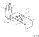
- Figure 1a shows a perspective view of a first embodiment of a conductor connection contact 1, which is formed in one piece from a piece of sheet material as a stamped and bent part.
- the conductor connection contact 1 has an insulation displacement contact connection 2 at one end.
- This insulation displacement contact connection 2 is formed from two contact fingers 3, which are aligned parallel to one another with an intermediate clamping slot 4 on a common plane and are connected to one another via a common root region 5.
- the free end sections of the contact fingers 3 are formed in a funnel-shaped manner toward the root region 5, for example by an inlet slope 6, so that the insertion of a wire bridge into the clamping slot 4 is facilitated.
- the mutually facing inner edges 7 of the contact fingers 3 clamp a wire bridge between them due to the spring force of the contact fingers 3 and the adjacent root section 5. They are designed as cut contacts at least to such an extent that the contact fingers 3 dig into the surface of an inserted wire bridge. However, they can also be sharp-edged in order to cut open an insulating jacket of a wire bridge, for example an insulated rigid or flexible electrical conductor, when inserted into the insulation displacement contact 2, in order in this way to expose the electrically conductive part of the wire bridge and to conduct it electrically to contact the contact fingers 3.
- connection contact 1 has a plug contact connection 8 on a connection surface 9.
- This connection surface 9 has a plug opening 10 and spring-elastic clamping tongues 11, which from the level of Pad 9 and out of the plug opening 10 and protrude towards each other.
- the clamping tongues 11 are cut or punched out of the sheet metal material of the connection surface 9 and protrude from opposite edge edges of the insertion opening 10.
- the insertion opening 10 is then delimited by opposite side webs 12.
- the conductor connection contact 1 has two solder connection surfaces 13a, 13b. It can be seen that the connection surface 9 lies on a level above the plane spanned by the solder connection surfaces 13a, 13b. Between the connection surface 9 and the solder connection surfaces 13a, 13b, foot sections 14 are provided, which connect to the connection surface 9 and lead to a respective solder connection surface 13a, 13b. In the exemplary embodiment shown, these foot sections 14 are designed as webs folded over from the connection surface 9. These are bent approximately at right angles from the connection surface 9.
- solder connection surfaces 13a, 13b can be formed at the end of the foot sections 14 or, as in the case of the solder connection surface 13a, merge from the foot section 14 into a solder connection surface 13a after a further bend.
- connection surface 13a merges into the insulation displacement contact connection 2 or its root section 5.
- This root section 5 with the adjoining contact fingers 3 extends approximately parallel to the foot section 14, so that the insulation displacement contact connection 2 and the foot section 14 are approximately perpendicular to the solder connection surface connecting the insulation displacement contact connection 2 to the foot section 14 13a stand.
- the connection surface 9, on the other hand, lies on a plane that lies transversely to the plane of extent of the insulation displacement contact connection 2.
- the insulation displacement contact connection 2 is thus aligned on a level that is perpendicular to the level of the connection surface 9.
- the plane of the connection surface 9 is at an angle of 90 ° +/- 45 ° to the plane of the insulation displacement contact connection 2.
- the conductor connection contact 1 can be stably soldered onto a circuit board. With the help of the transition from the first soldering connection surface 13a to the insulation displacement contact connection 2 projecting therefrom, this is also stably connected to a printed circuit board with short current paths.
- Figure 1b shows a compared to the embodiment of Figure 1a ) somewhat modified variant of the conductor connection contact 1.
- a material flap 3 is provided on the connection surface 9 at a distance from the horizontal solder connection surface 13a, which is cut free from the bend which merges into the foot section 14 and enlarges the flat surface of the connection surface 9 in the region of the bend. This increases the suction area for the automatic handling and assembly of the conductor connection contact 1.
- the material tab 33 is provided on the side of the insulation displacement contact connection 2 and extends in the direction of this insulation displacement contact connection 2.
- such a material tab 33 on the opposite side at a distance from the solder connection surface 13b) is present or that such cloths are provided on both sides. This also depends specifically on the position of the plug opening 10 on the connection surface 9.
- solder connection surface 13b) merges into a bend on the right side from the foot section 14 and provides a flat support.
- This solder connection surface 13b) is therefore not as in FIG Figure 1a ) formed only by the lower edge of the foot section 14, but by a surface section extending transversely from the foot section 14 after a bend.
- the insulation displacement contact connection 2 is also made in comparison to the embodiment Figure 1a ) slightly modified. It becomes clear that the outer edges of the contact fingers 3, which are each opposite the clamping slot 4, are concavely curved toward the clamping slot. This is the width of the insulation displacement contact connection 2 in the area of the contact slot is lower than in the area of the inlet slopes 6. In this way, the spring force of the contact fingers 3 can be improved.
- connection area 9 is spaced from the plane of the solder connection areas 13a, 13b, which is achieved by the foot areas 14. It can also be seen that the insulation displacement contact connection 2 lies on a plane which is transverse to the plane of the connection surface 9.
- the clamping tongues 11 of the spring clamping element are bent toward one another out of the plane of the connection surface 9 and away from the plane of the solder connection surfaces 13a, 13b.
- the freely movable ends of the resilient clamping tongues 11 have clamping edges 15 to form a plug contact in order to clamp an electrical conductor or contact pin inserted between them in the plug-in opening 10 in the plug-in direction S and thus to make electrical contact therewith.
- Figure 2b omits a side view of the modified conductor connection contact 1 Figure 1b ) detect. It is clear here that the material flap 33 extends at a distance from the soldering connection surface 13a on the level of the connection surface 9 in the direction of the insulation displacement contact connection 2, so as to enlarge the suction surface for an automatic handling machine.
- solder connection surface 13b is not simply formed from the lower edge of the foot section 4, but rather from a surface section which extends away from the foot section 4.
- the contact fingers 3 of the insulation displacement connection taper conically in terms of their width towards the free end. This means that the material thickness of the contact fingers 3 decreases towards their free end.
- Figure 3 omits a front view of the conductor connection contact 1 Figures 1a and 2a detect. It becomes clear that the contact fingers 3 are formed from the sheet metal material while leaving an intermediate clamping slot 4 and merge into a common root area 5. The contact fingers 3 taper towards the free end, the inner edges there forming an insertion funnel on an inclined surface 6.
- the insulation displacement contact connection 2 is thus designed in the manner of a fork contact in order to insert a wire bridge inserted into the clamping slot 4 in the form of a non-insulated rod with a round cross section, an insulated rigid or flexible electrical conductor or a round, rectangular or cross section otherwise to be connected as a suitable conductor rail.
- connection surface 9 has a plug opening 10, from the opposite edge regions of which the spring-elastic clamping tongues 11 project to form a spring clamping element. An electrical conductor can thus be inserted from the bottom through the plug opening 10 and clamped with the spring-elastic clamping tongues 11.
- the insulation displacement contact connection 2 on the left side of the conductor connection contact 1 in the figure extends on a plane that is perpendicular to the plane of the conductor connection surface 9.
- the contact fingers 3 of the insulation displacement contact connection 2 lie on a plane that is transverse to the longitudinal direction of the conductor connection contact 1 and its connection surface 9. The direction of longitudinal extension is the direction from the insulation displacement contact connection 2 to the plug contact connection 8.
- Figure 5 reveals a second embodiment of a conductor connection contact 1. In principle, this is constructed similarly to the first embodiment. Only the insulation displacement contact connection 2 is rotated relative to the direction of extension of the conductor connection contact 1. It can be seen that the contact fingers 3 now lie on a common plane, which extends transversely to the plane of the connection surface 9 and in the longitudinal direction of the connection surface 9, ie towards the plug contact connection 8. Thus, the direction of extension of a wire bridge clamped to the insulation displacement contact connection 2 lies in the clamping region transversely to the direction of longitudinal extension of the conductor connection contact 1, while the direction of extension of the insulation displacement contact contact 2 is oriented in the longitudinal direction of extension of the conductor connection contact 1 in the first embodiment.
- connection surface 9 does not necessarily have to be a flat surface, as shown. It can also be a curved surface which merges into adjoining curved or straight foot sections 14. However, it is also conceivable for the connection surface 9 to have a pointed roof in cross section, with foot sections 9 extending obliquely to the level of the printed circuit board.
- FIG 6a shows a perspective cutout view of a circuit board arrangement 16.
- This circuit board arrangement 16 has at least two circuit boards 17a, 17b arranged next to one another, on each of which at least one conductor connection contact 1 is soldered. It can be seen that the connection surface 9 with the plug contact connection 8 is supported on the level of the printed circuit board 17a, 17b by means of the mutually opposite foot sections 14 or is spaced apart from the plane of the printed circuit board 17a, 17b. Furthermore, it is clear that a conductor lead-through opening 18 is made in the printed circuit board below the plug opening 10 of the plug contact connection 8.
- the conductor feed-through opening 18 is aligned with the plug-in opening 10 such that its center of gravity is preferably on a common vertical of the printed circuit board 17b, so that an electrical conductor can be guided through the conductor feed-through opening 18 into the plug-in opening 10 in order to be clamped there at the plug contact connection 8.
- a common main section 21 is bent from the mutually opposite end sections 20a, 20b of the wire bridge 19, which extends transversely to the longitudinal direction of the conductor connection contacts 1 and thus also transversely to the direction of extension of the gap between the two printed circuit boards 17a, 17b.
- the wire bridge 19 would then simply have to be inserted rotated by 90 °, so that the main section 21 extends in the direction of extension of the conductor connection contacts 1 and the adjacent edge edges or the space between the printed circuit boards 17a, 17b.
- the end sections 20a, 20b would then be clamped to the respective insulation displacement contact connection 2 in their direction of extension transverse to the direction of longitudinal extension of the conductor connection contacts 1.
- Figure 6b shows one compared to the Figure 6a ) slightly modified perspective cut-out view of a circuit board arrangement 16, in which the insulation displacement contact connections 2 are aligned in such a way that the planes spanned by the contact fingers 3 face each other, that is to say assign them to one another. These levels are aligned parallel to each other. Therefore, the end sections 20a, 20b inserted into the clamping slots 4 are each oriented towards the opposite printed circuit board 17a, 17b.
- an embodiment wound through a loop-like section 34 is used. This ensures tolerance compensation in the event of a shift in the position of the printed circuit board arrangement 16.
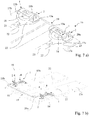
- Figure 7a reveals the opposite side of the printed circuit board 17b with an additional printed circuit board 17c of the printed circuit board arrangement 16 adjoining it.
- the printed circuit boards 17b, 17c lying next to one another on their longitudinal edge are now connected to one another in an electrically conductive manner.
- a wire bridge is again provided, which is designed as a non-curved, straight rod or electrical conductor.
- the free end sections 20a, 20b can be bent transversely to the plane without further bending of the wire bridge 19 the insulation displacement contact connections 2 are clamped to it.
- the printed circuit boards 17a, 17b, 17c carry electrical or electronic components 22, such as in particular light-emitting diodes.
- This circuit board arrangement 16 can thus be used for a lamp.
- the circuit boards 17a, 17b, 17c carry conductor tracks 23, which are soldered to the respective solder connection surfaces 13a, 13b with a respective conductor connection contact 1. Electrical energy can thus be supplied to the electrical / electronic components 22 to be supplied via the conductor connection contacts 1.
- Figure 7b shows a modified embodiment of a circuit board arrangement 16, in which the interconnected insulation displacement contact connections 2 are aligned such that the clamping slots 4 are not as in the exemplary embodiment according to FIG Figure 7a ) are aligned to each other. Therefore, the end sections 20a, 20b of the wire bridge 19 extend approximately parallel to one another in the same main direction of extension. The two end sections 20a, 20b are connected to one another by a cross bar 35.
- the wire bridge 19 is designed in the manner of a U-shaped element.
- Figure 8 shows a perspective detail view of the circuit board arrangement 16 in an area where electrical conductors 24 are each guided through a conductor lead-through opening 18 in the circuit board and the plug-in opening 10 of the conductor connection contact 1 lying above it.
- the free stripped end of an electrical conductor 24 is then clamped to the clamping edges of the spring-elastic clamping tongues 11 and contacted there in an electrically conductive manner and held mechanically firmly.
- a voltage potential can thus be applied to the printed circuit board arrangement 16 in order to supply the electrical / electronic components 22 with electrical power.
- the insulation displacement contact connections 2 are not assigned, as shown, when the electrical / electronic components 22 and their circuit boards 17a, 17b, 17c, 17d, 17e are connected in series.
- the insulation displacement contact connections 2 also carry a wire bridge 19 in order not only to transmit the electrical power via the conductor tracks 23 to the opposite conductor connection terminal 1 of the same printed circuit board 17a, 17b, 17c, 17d, 17e, but directly to an adjacent circuit board 17a, 17b, 17c, 17d, 17e.
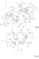
- Figure 9 omits a sectional view of the circuit board arrangement 16 Figure 8 recognize with electrical conductor 24 clamped to it.
- the printed circuit board 17d is supported on a carrier element 25.
- This carrier element 25 can, for example, be a sheet metal housing of a lamp.
- a through opening 26 is introduced into the carrier element 25 in alignment with the conductor lead-through opening 18 of the printed circuit board 17 d and is closed with a lead-through seal 27.
- the electrical conductor 24 is then passed through the opening of the lead-through seal 27 in order to be contacted in an electrically conductive manner at a plug contact connection 8 as shown.
- a lens element 28 for example made of transparent plastic, is placed on the carrier element 25 in order to cover the lamp arrangement and to emit light emitted by the electronic components 22 in the form of light-emitting diodes as uniformly or as focused as possible.
- webs 29 of the lens element 28 in the region of the Protect insulation displacement contact connections 2. These webs 29 accommodate, for example, an insulation displacement contact connection 2 on both sides in a groove in a web 29.
- a slot is then present in the web 29 in the region of the intermediate space between the clamping fingers 3 in order to lead a wire bridge 19 through the web 29 and to clamp it on the assigned insulation displacement contact connection 2.
- the wire bridges 19 can be inserted into these webs 29, so that by placing the carrier element 25 with the preassembled printed circuit boards 17a, 17b, 17c, 17d on the lens element 28, the wire bridge 19 into the clamping slots 4 of the insulation displacement contact connections 2 are introduced.
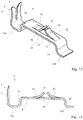
- Figure 10 omits a perspective view of a section of a lamp arrangement 30 with the carrier element 25 Figure 9 and recognize strip-shaped printed circuit boards 17a, 17b, 17c, 17d installed therein. It becomes clear that each printed circuit board 17a, 17b, 17c, 17d carries conductor connection contacts 1 at their opposite ends adjacent to the narrow edges. These are arranged symmetrically with respect to one another, so that the insulation displacement contact connections 2 of such a pair of conductor connection contacts 1 each point to the other longitudinal edge or are arranged adjacent to the respective other longitudinal edge 31a, 31b.
- electrical conductors 24 are inserted from the underside of the carrier element 25 transversely to the plane of the printed circuit boards 17d, 17c in order to be clamped to the plug contact connections of these conductor connection contacts 1.
- the carrier element 25 is closed with an end cap 32, which is attached to the profile of the carrier element 25.
- Figure 11 shows a perspective view of a further embodiment of a conductor connection contact 1. This differs from the conductor connection contacts 1 described above in that there is no insulation displacement contact connection 2 for connecting an additional electrical conductor or a wire bridge. These conductor connection contacts 1 are provided, in particular, for the end connections of a lamp arrangement 30 to which energy supply / discharge lines are connected.
- Figure 12 reveals a modified embodiment of a conductor connection contact 1, in which the clamping tongues 11 are provided with a further bend 36 or a kink.
- the clamping tongues 11 are arranged at a greater angle to one another in their region which adjoins the connection surface 9 (ie at a flatter angle) than in the region adjoining the clamping edges 15.
- the section of the clamping tongues 11 adjoining the clamping edges 15 is thus steeper than the area of the clamping tongues 11 which merges into the connecting surface 9. This leads to a reduction in the insertion forces for the insertion of an electrical conductor and a loosening of a connected electrical conductor Conductor by turning and pulling is possible.
- This configuration of the clamping tongues 11 is in Figure 13 even clearer from the page display.
- the sections of the clamping tongues 11 adjoining the clamping edges 15 are arranged at an acute angle in the rest position without an inserted electrical conductor, while the sections of the clamping tongues 11 adjoining the connection surface 9 are aligned at an obtuse angle to one another are. This does not change even when an electrical conductor is clamped in, since both angles decrease due to the further raising of the clamping tongues 11, the relationship between obtuse angle and acute angle is still maintained.
- Figure 14 omits a perspective view of the modified embodiment Figures 12 and 13 detect.
- these bends 36 can also be made from other configurations of the conductor connection contacts 1, in particular the conductor connection contacts 1 Figure 1a ) and Figure 11 equally be provided.
- the clamping tongues are bent obliquely out of the connection surface 9 so that they point towards one another. Due to the bends 26 or a kink, the angle between the opposite sections of the clamping tongues 11 is reduced. As a result, the insertion forces for an electrical conductor inserted through the plug opening 10 are reduced and the conductor can be removed from the plug connection 8 by rotating and pulling.
- connection contact similar to that previously based on the Figure 11 explained conductor connection contact, a plug contact connection 8a in the connection surface 9.
- Two spring-elastic clamping tongues 11a are bent out of the material of the conductor connection contact 1, so that a plug opening 10a is formed there.
- the connection area 9 is also spaced apart from the plane of the solder connection areas 13a, 13b in that the ends of the conductor connection contact 1, which have the solder connection areas 13a, 13b, are connected to the connection area 9 via foot sections 14, which may run essentially vertically to the connection area 9, for example are.
- foot sections 14 in this embodiment can be somewhat extended compared to the embodiment of FIG Figure 11 be trained.
- a further plug contact connection 8b can, for example, be formed in one or in both foot sections 14.
- the Figures 15 and 16 each show only one further plug contact connection 8b in a foot section 14.
- the further plug contact connection 8b is formed by protruding a spring-elastic clamping tongue 11b from the material of the foot section 14, so that a plug opening 10b is formed there.
- the resilient clamping tongue 11b has a clamping edge. An electrical conductor can then be clamped between the underside of the connection surface 9 facing the clamping tongue 11b and this clamping edge.
- the plug contact connection 8a formed in the connection surface 9 has an insertion direction S which runs essentially perpendicular to the connection surface 9.
- the insertion direction S can, as in Figure 16 shown, run from bottom to top, or in the opposite direction if the spring-elastic clamping tongues 11a are bent out (downward) to the other side of the connection surface 9.
- the further plug contact connection 8b has a conductor insertion direction W which is essentially perpendicular to the conductor insertion direction S.
- an electrical conductor to be inserted can be inserted either horizontally (conductor insertion direction W) or vertically (conductor insertion direction S) to the connection surface 9 and accordingly to the circuit board parallel to it. If necessary, respective electrical conductors can also be plugged into both plug contact connections 8a, 8b.
- a conductor insertion tongue 110 is bent out in the opposite direction from the material of the conductor connection contact 1 on the opposite edge of the plug opening 10b, at which the spring-elastic clamping tongue 11b is not bent out, i.e. the conductor insertion tongue 110 points to the right in the opposite direction of the conductor insertion W.
- This forms a funnel-shaped conductor insertion which facilitates the insertion of an electrical conductor into the further plug contact connection 8b.
- the Figures 17 and 18 show a circuit board 17 with attached conductor connection contact according to the Figures 15 to 16 . It can be seen in particular in the Figure 18 the possibility of inserting an electrical conductor 24a vertically to the printed circuit board 17, and optionally or additionally an electrical conductor 24b horizontally to the printed circuit board 17.
- the conductor connection contact 1 projects according to the illustration in FIG Figures 17 and 18 through an opening in the printed circuit board 17 so that the overall height is reduced compared to the arrangement of the conductor connection contact 1 on the printed circuit board, as is shown, for example, in FIG Figure 8 is shown.
Abstract
Ein Leiteranschlusskontakt (1) mit einer Lötanschlussfläche (13a, 13b) zur Anbindung an eine Leiterplatte (17a, 17b, 17c, 17d, 17e), und einem Steckkontaktanschluss (8) mit mindestens einem Federklemmelement wird beschrieben.Der Steckkontaktanschluss (8) ist an einer Anschlussebene (9) des Leiteranschlusskontaktes (1) gebildet, die von der Ebene der Lötanschlussflächen (13a, 13b) beabstandet ist und eine Stecköffnung (10) und mindestens eine federelastische Klemmzunge (11) zur Bildung des Federklemmelementes hat. Die Anschlussfläche (9) geht in Fußabschnitte (14) über, die jeweils mit einer Lötanschlussfläche (13a, 13b) verbunden sind oder eine Lötanschlussfläche (13a, 13b) an ihrer, der Anschlussfläche (9) abgewandten Seite haben.A conductor connection contact (1) with a solder connection surface (13a, 13b) for connection to a printed circuit board (17a, 17b, 17c, 17d, 17e) and a plug contact connection (8) with at least one spring clamp element is described. The plug contact connection (8) is on a connection plane (9) of the conductor connection contact (1) is formed, which is spaced from the plane of the solder connection surfaces (13a, 13b) and has a plug opening (10) and at least one spring-elastic clamping tongue (11) to form the spring clamping element. The connection surface (9) merges into foot sections (14), which are each connected to a solder connection surface (13a, 13b) or have a solder connection surface (13a, 13b) on their side facing away from the connection surface (9).
Description
Die Erfindung betrifft einen Leiteranschlusskontakt mit einer Lötanschlussfläche zur Anbindung an eine Leiterplatte und einem Steckkontaktanschluss mit einem Federklemmelement.The invention relates to a conductor connection contact with a solder connection surface for connection to a printed circuit board and a plug contact connection with a spring clamp element.
Die Erfindung betrifft weiterhin eine Leiterplattenanordnung mit einer Leiterplatte, wobei ein Leiteranschlusskontakt mit seinen Lötflächen auf der Leiterplatte aufgelötet ist.The invention further relates to a circuit board arrangement with a circuit board, a conductor connection contact being soldered to the circuit board with its soldering areas.
Leiterplatten mit darauf aufgebrachten elektrischen/elektronischen Bauelementen haben zur elektrisch leitfähigen Verbindung von Leitern oder zur Verbindung benachbarter Leiterplatten miteinander Leiteranschlusskontakte. Diese werden in Durchsteckmontage oder Oberflächenmontage auf die Leiterplatte aufgelötet und mit dieser elektrisch und mechanisch verbunden.Printed circuit boards with electrical / electronic components mounted on them have conductor connection contacts for the electrically conductive connection of conductors or for connecting adjacent printed circuit boards to one another. These are soldered onto the PCB in a push-through or surface mounting and connected to it electrically and mechanically.
Ausgehend hiervon ist es Aufgabe der vorliegenden Erfindung, einen verbesserten Leiteranschlusskontakt und eine verbesserte Leiterplattenanordnung zu schaffen, wobei der Leiteranschlusskontakt möglichst kompakt, gut handhabbar und stabil ist und dabei einen zuverlässigen elektrischen Kontakt sicherstellt.Proceeding from this, it is an object of the present invention to provide an improved conductor connection contact and an improved printed circuit board arrangement, the conductor connection contact being as compact as possible, easy to handle and stable, and thereby ensuring reliable electrical contact.
Die Aufgabe wird mit dem Leiteranschlusskontakt mit den Merkmalen des Anspruchs 1 sowie der Leiterplattenanordnung mit einem solchen Leiteranschlusskontakt mit den Merkmalen des Anspruchs 9 gelöst. Vorteilhafte Ausführungsformen sind in den Unteransprüchen beschrieben.The object is achieved with the conductor connection contact with the features of
Dadurch, dass der Steckkontaktanschluss an einer Anschlussfläche des Leiteranschlusskontaktes gebildet ist, die von der Ebene der Lötanschlussfläche beabstandet ist, kann bei kompakten Aufbau die Einhaltung von notwendigen Luft- und Kriechstrecken sichergestellt werden. Dabei hat die Anschlussfläche eine Stecköffnung und mindestens eine federelastische Klemmzunge zur Bildung des Federklemmelementes. Dies ermöglicht das einfache Anklemmen eines elektrischen Leiters, der durch die Stecköffnung hindurchgesteckt und mittels der federelastischen Klemmzunge an der Anschlussfläche des Steckkontaktanschlusses festgeklemmt wird.Because the plug contact connection is formed on a connection surface of the conductor connection contact which is spaced from the plane of the solder connection surface, the necessary clearance and creepage distances can be ensured with a compact construction. The connection surface has a plug opening and at least one spring-elastic clamping tongue to form the spring clamping element. This enables the simple connection of an electrical conductor which is inserted through the plug-in opening and clamped to the connection surface of the plug-in contact connection by means of the spring-elastic clamping tongue.
Die Anschlussfläche geht dann in einen Fußbereich über, der jeweils mit einer Lötanschlussfläche verbunden ist oder eine Lötanschlussfläche an seiner der Anschlussfläche abgewandten Seite hat. Auf diese Weise wird die Anschlussfläche beabstandet von der Ebene der Leiterplatte mit Hilfe der Fußbereiche stabil gelagert. Die an die Fußbereiche angrenzenden Lötanschlussflächen stellen dabei sicher, dass der Steckkontaktanschluss bei Verlöten des Lötanschlusskontaktes auf einer Leiterplatte an den Lötanschlussflächen stabil gehalten wird. Der Stromfluss geht dann über die Fußbereiche direkt zur Lötanschlussfläche, sodass die stromleitenden Querschnitte und Wege optimiert sind.The connection area then merges into a foot region, which is in each case connected to a solder connection area or has a solder connection area on its side facing away from the connection area. In this way, the connection area is stably supported at a distance from the plane of the printed circuit board with the aid of the foot regions. The solder connection areas adjoining the foot areas ensure that the plug contact connection is kept stable on the solder connection areas when the solder connection contact is soldered to a printed circuit board. The current flow then goes through the foot areas directly to the solder connection surface, so that the current-conducting cross-sections and paths are optimized.
An den einander gegenüberliegenden Randkanten der Stecköffnung können federelastische Klemmzungen aufeinander zu weisend herausgebogen sein. Die freibeweglichen Enden der Klemmzungen bilden dann Klemmkanten zum Anklemmen eines in die Stecköffnung eingesteckten elektrischen Leiters oder Kontaktstiftes. Damit kann ein elektrischer Leiter oder Kontaktstift bei überaus einfachem Aufbau des Leiteranschlusskontaktes sehr zuverlässig angeklemmt werden. Die Stromwege führen dann auf kürzestem Wege über die Klemmzungen und die Fußabschnitte zu den Lötanschlussflächen.At the opposite edge of the plug-in opening, resilient clamping tongues can be bent out to point towards each other. The freely movable ends of the clamping tongues then form clamping edges for clamping an electrical conductor or contact pin inserted into the insertion opening. An electrical conductor or contact pin can thus be connected very reliably with an extremely simple construction of the conductor connection contact. The current paths then lead the shortest way over the clamping tongues and the foot sections to the solder connection areas.
An den Leiteranschlusskontakt kann weiterhin ein Schneid-Klemm-Kontaktanschluss vorhanden sein.An insulation displacement contact connection can also be present on the conductor connection contact.
Eine Lötanschlussfläche kann zwischen einem Schneid-Klemm-Kontaktanschluss und einem zur Anschlussebene führenden Steg angeordnet sein. Dies hat den Vorteil, dass der Schneid-Klemm-Kontaktanschluss und die Anschlussfläche über die gemeinsame Lötanschlussfläche miteinander verbunden sind, wobei die Stromwege zwischen Schneid-Klemm-Kontaktanschluss und Steckkontaktanschluss kurz sind und der Schneid-Klemm-Kontaktanschluss und der Steckkontaktanschluss über die gemeinsame Lötanschlussfläche mechanisch stabilisiert sind.A solder connection surface can be arranged between an insulation displacement contact connection and a web leading to the connection level. This has the advantage that the insulation displacement contact connection and the connection surface are connected to one another via the common solder connection surface, the current paths between insulation displacement connection contact terminal and plug contact connection being short and the insulation displacement contact connection and the plug contact connection via the common solder connection surface are mechanically stabilized.
Der Schneid-Klemm-Kontaktanschluss kann zwei voneinander beabstandete Kontaktfinger haben, die in einem gemeinsamen Wurzelabschnitt miteinander verbunden sind. Der Wurzelabschnitt geht dann in den Fußabschnitt über oder bildet den Fußabschnitt. So ist denkbar, dass der Wurzelabschnitt in eine der Lötanschlussflächen übergeht. Dies führt dann zu einem sehr kompakten Aufbau des Lötanschlusskontaktes.The insulation displacement contact connection can have two spaced-apart contact fingers which are connected to one another in a common root section. The root section then merges into the foot section or forms the foot section. It is conceivable that the root section merges into one of the solder connection surfaces. This then leads to a very compact structure of the solder connection contact.
Die Erstreckungsrichtung einer an dem Schneid-Klemm-Kontaktanschlusses angeklemmten Drahtbrücke im Klemmbereich an dem Schneid-Klemm-Kontaktanschluss kann quer zur Steckrichtung des Steckkontaktanschlusses ausgerichtet sein. Die Erstreckungsrichtung der Drahtbrücke an dem Schneid-Klemm-Kontaktanschluss im Bereich der Klemmstelle, in der eine Drahtbrücke zur Klemmstelle zwischen die Kontaktfinger geführt wird, verläuft hingegen in Steckrichtung des Steckkontaktanschlusses. Die von Kontaktfingern des Schneid-Steckkontaktanschlusses oder einer geschlitzten Wand zur Bildung des Schneid-Steck-Kontaktanschlusses aufgespannte Ebene ist somit quer zur Ebene der Anschlussfläche ausgerichtet. Unter "quer" wird eine Ausrichtung im Winkelbereich von 90° +/- 20° und bevorzugt 90° +/- 5° verstanden.The direction of extension of a wire bridge clamped to the insulation displacement contact connection in the clamping region on the insulation displacement contact connection can be oriented transversely to the direction of insertion of the plug contact connection. The direction of extension of the wire bridge at the insulation displacement contact connection in the region of the clamping point, in which a wire bridge is guided to the clamping point between the contact fingers, runs in the plugging direction of the plug contact connection. The plane spanned by contact fingers of the cutting plug contact connection or a slotted wall to form the cutting plug contact connection is thus oriented transversely to the plane of the connection surface. "Transversal" means an orientation in the angular range of 90 ° +/- 20 ° and preferably 90 ° +/- 5 °.
Die Erstreckungsrichtung der an dem Schneid-Klemm-Kontaktanschluss angeklemmten Drahtbrücke im Klemmbereich dieses Schneid-Klemm-Kontaktanschlusses kann dabei in Erstreckungsrichtung der Anschlussfläche oder auch quer zur Erstreckungsrichtung der Anschlussfläche sein. Denkbar ist aber auch, dass sie schräg zur Erstreckungsrichtung der Anschlussfläche ausgerichtet ist. Die Leiterplattenanordnung hat eine Leiterplatte, bei der ein solcher Leiteranschlusskontakt mit seinen Lötflächen auf der Leiterplatte aufgelötet ist. Die Leiterplatte hat dann unterhalb von der Stecköffnung eine Leiterdurchführungsöffnung, sodass ein elektrischer Leiter durch die Leiterdurchführungsöffnung in die Stecköffnung eingesteckt und an dem Steckkontaktanschluss angeklemmt werden kann. Dies ermöglicht eine sehr kompakte Anbindung eines elektrischen Leiters an die Leiterplatte mit einer Steckrichtung lotrecht zur Leiterplatte.The direction of extension of the wire bridge clamped to the insulation displacement contact connection in the clamping region of this insulation displacement contact connection can be in the direction of extension of the connection surface or also transverse to the direction of extension of the connection surface. However, it is also conceivable that it is oriented obliquely to the direction of extension of the connection surface. The circuit board arrangement has a circuit board in which such a conductor connection contact is soldered onto the circuit board with its soldering areas. The circuit board then has a conductor lead-through opening below the plug-in opening, so that an electrical conductor can be inserted through the conductor lead-through opening into the plug-in opening and clamped on the plug contact connection. This enables a very compact connection of an electrical conductor to the circuit board with a plug-in direction perpendicular to the circuit board.
Die Anschlussfläche des Leiteranschlusskontaktes kann sich dabei parallel zur Ebene der Leiterplatte erstrecken. Ein den Schneid-Klemm-Kontaktanaschluss aufweisender Abschnitt des Leiteranschlusskontaktes ragt dann von der Ebene der Leiterplatte ab.The connection area of the conductor connection contact can extend parallel to the plane of the circuit board. A section of the conductor connection contact having the insulation displacement contact connection then protrudes from the plane of the circuit board.
Von der Anschlussfläche kann ein Materiallappen im Abstand zu einem der Lötanschlussflächen, z.B. in Richtung eines Schneid-Klemm-Kontaktanschlusses abragen. Damit wird die Anschlussfläche benachbart zu dem Steckkontaktanschluss vergrößert. Dieser Materiallappen (auch als Lasche bezeichnet) dient der Bereitstellung einer vergrößerten Ansaugfläche für eine automatisierte Handhabung und Montage der Leiteranschlusskontakte.A material flap can be spaced from the connection surface to one of the solder connection surfaces, e.g. protrude in the direction of an insulation displacement contact connection. The connection area adjacent to the plug contact connection is thus enlarged. This material flap (also known as a flap) is used to provide an enlarged suction surface for automated handling and assembly of the conductor connection contacts.
Die Klemmfederzungen können in einem der jeweiligen Klemmkante vorgelagerten Bereich einen Knick oder eine Biegung haben. Die aufeinander zuweisend herausgebogenen Klemmzungen sind hierdurch in dem an die Anschlussfläche angrenzenden Bereichen in einem größeren Winkel zueinander ausgerichtet, als in dem an die Klemmkante angrenzenden Bereich. Durch den Knick oder die Biegung sind die an den Klemmkanten angrenzenden Flächen der einander gegenüberliegenden Klemmzungen somit in einem spitzeren Winkel zueinander angeordnet. Diese zusätzlichen Biegungen bzw. Knicke führen zu einer Verringerung der Einsteckkräfte und ermöglichen das Lösen eines angeschlossenen Leiters durch Drehen und Ziehen des angeklemmten Leiters.The clamping spring tongues can have a kink or a bend in an area upstream of the respective clamping edge. As a result, the clamping tongues bent out toward one another are oriented at a greater angle to one another in the regions adjacent to the connection surface than in the region adjacent to the clamping edge. Due to the kink or the bend, the surfaces of the opposing clamping tongues adjoining the clamping edges are thus arranged at an acute angle to one another. These additional bends or kinks lead to a reduction in the insertion forces and enable a connected conductor to be released by rotating and pulling the clamped conductor.
Gemäß einer vorteilhaften Weiterbildung der Erfindung ist vorgesehen, dass die Einsteckrichtung zum Einstecken eines elektrischen Leiters in den Steckkontaktanschluss im Wesentlichen senkrecht zur räumlichen Erstreckung wenigstens einer der Lötanschlussflächen verläuft. Auf diese Weise kann der elektrische Leiter bequem quer zur räumlichen Erstreckung der Leiterplatte von der Oberseite oder der Unterseite in den Steckkontaktanschluss eingesteckt werden.According to an advantageous development of the invention, it is provided that the direction of insertion for inserting an electrical conductor into the plug contact connection is substantially perpendicular to the spatial extent of at least one of the solder connection surfaces. In this way, the electrical conductor can be conveniently inserted into the plug contact connection transversely to the spatial extent of the printed circuit board from the top or the bottom.
Gemäß einer vorteilhaften Weiterbildung der Erfindung ist vorgesehen, dass an einer Randkante der Stecköffnung eine federelastische Klemmzunge und an einer dieser Randkante gegenüberliegenden Randkante der Stecköffnung eine Leitereinführzunge angeordnet ist, wobei die Klemmzunge und die Leitereinführzunge voneinander fortweisend herausgebogen sind. Auf diese Weise kann die Leitereinführzunge eine Leitereinführschräge zum vereinfachten Einführen eines elektrischen Leiters zu einer mit einem frei beweglichen Ende der Klemmzunge gebildeten Klemmstelle bilden. Die Leitereinführzunge ist dabei nicht unbedingt selbst Teil der Klemmstelle oder muss auch nicht zwangsläufig ein Gegenlager bei der Klemmung des elektrischen Leiters durch die Klemmzunge bilden. Das Gegenlager kann z.B. durch die Anschlussfläche des Leiteranschlusskontaktes gebildet sein.According to an advantageous development of the invention, it is provided that a resilient clamping tongue is arranged on an edge of the plug-in opening and a conductor insertion tongue is arranged on an edge of the plug-in opening opposite this edge, the clamping tongue and the conductor insertion tongue being bent away from each other. In this way, the conductor insertion tongue can form a conductor insertion slope for the simplified insertion of an electrical conductor to a clamping point formed with a freely movable end of the clamping tongue. The conductor insertion tongue is not necessarily part of the clamping point itself or does not necessarily have to form a counter bearing when the electrical conductor is clamped by the clamping tongue. The counter bearing can e.g. be formed by the connection surface of the conductor connection contact.
Gemäß einer vorteilhaften Weiterbildung der Erfindung ist vorgesehen, dass der Leiteranschlusskontakt einen weiteren Steckkontaktanschluss aufweist, dessen Einsteckrichtung zum Einstecken eines Leiters in den weiteren Steckanschluss im Wesentlichen orthogonal zu einer Einsteckrichtung des an der Anschlussfläche gebildeten Steckkontaktanschlusses verläuft. Dies hat den Vorteil, dass die Verdrahtungsrichtung von in dem Leiteranschlusskontakt einzusteckenden elektrischen Leitern im Nachhinein ausgewählt werden kann, z.B. bei bereits an einer elektrischen Leiterplatte befestigtem Leiteranschlusskontakt. Es kann somit wahlweise ein elektrischer Leiter senkrecht zur elektrischen Leiterplatte eingesteckt werden (in den Steckkontaktanschluss an der Anschlussfläche) oder waagerecht zur Leiterplatte (in den Steckanschluss in zumindest einem der Fußabschnitte). Somit muss bei dem erfindungsgemäßen Leiteranschlusskontakt nicht von vornherein festgelegt werden, ob die Leiterplatten, z.B. LED-Module, auf der Leiterplattenoberseite oder der Leiterplattenunterseite verdrahtet werden. Es sind vielmehr beide Möglichkeiten weiterhin gegeben.According to an advantageous development of the invention, it is provided that the conductor connection contact has a further plug contact connection, the insertion direction of which for inserting a conductor into the further plug connection is essentially orthogonal to an insertion direction of the plug contact connection formed on the connection surface. This has the advantage that the wiring direction of electrical conductors to be inserted in the conductor connection contact can be selected afterwards, for example if the conductor connection contact is already attached to an electrical circuit board. An electrical conductor can thus either be inserted perpendicular to the electrical circuit board (in the plug contact connection on the connection surface) or horizontally to the circuit board (in the plug connection in at least one of the foot sections). Thus, with the conductor connection contact according to the invention, it does not have to be determined from the outset whether the printed circuit boards, for example LED modules, are on the upper side of the printed circuit board or the underside of the PCB. Rather, both options are still available.
Der weitere Steckkontaktanschluss kann z.B. an einem Fußabschnitt des Leiteranschlusskontaktes gebildet sein. Der Leiteranschlusskontakt kann auch mehrere weitere Steckkontaktanschlüsse mit der genannten orthogonalen Einsteckrichtung aufweisen, z.B. in jedem der Fußabschnitte einen solchen Steckkontaktanschluss oder mehrere solche Steckkontaktanschlüsse. Auf diese Weise kann z.B. ein Durchschleifen eines elektrischen Potenzials von einer Leiterplatte zur nächsten Leiterplatte realisiert werden.The further plug contact connection can e.g. be formed on a foot section of the conductor connection contact. The conductor connection contact can also have a plurality of further plug contact connections with the mentioned orthogonal insertion direction, e.g. one or more such plug contact connections in each of the foot sections. In this way e.g. looping through an electrical potential can be realized from one circuit board to the next circuit board.
Durch die Kombination eines vertikalen und eines horizontalen Leiteranschlusses an ein und demselben Leiteranschlusskontakt, z.B. einer SMD-Klemme, können Leiterplatten sowohl vertikal (von der Rückseite der Leiterplatte) als auch horizontal (auf der Oberseite der Leiterplatte) verdrahtet werden. Somit müssen keine Leiterplatten für den jeweiligen Anwendungszweck mit speziell geformten Leiteranschlusskontakten hergestellt werden. Stattdessen kann eine Leiterplatte für beide Verdrahtungsarten hergestellt und eingesetzt werden. Zum Beispiel können Leuchtenhersteller ein einziges LED-Modul mit einem solchen Leiteranschlusskontakt für vorderseitig und rückseitig verdrahtete Leuchten einsetzen.By combining a vertical and a horizontal conductor connection on one and the same conductor connection contact, e.g. an SMD terminal, circuit boards can be wired both vertically (from the back of the circuit board) and horizontally (on the top of the circuit board). This means that no circuit boards for the respective application need to be manufactured with specially shaped conductor connection contacts. Instead, a circuit board can be manufactured and used for both types of wiring. For example, luminaire manufacturers can use a single LED module with such a conductor connection contact for luminaires wired on the front and rear.
Die Einsteckrichtung des erstgenannten Steckkontaktanschlusses, der an der Anschlussfläche des Leiteranschlusskontaktes gebildet ist, kann wahlweise zu der Vorderseite oder der Rückseite der Leiterplatte hin weisen, d.h. von der Seite des Leiteranschlusskontakts, an der die Fußabschnitte von der Anschlussfläche abragen, oder von der gegenüberliegenden Seite der Anschlussfläche. Somit kann auch für beide Kontaktierungsrichtungen auf der Leiterplattenoberseite eine Verdrahtung ermöglicht werden.The insertion direction of the first-mentioned plug contact connection, which is formed on the connection surface of the conductor connection contact, can optionally point towards the front or the back of the circuit board, i.e. from the side of the conductor connection contact on which the foot sections protrude from the connection area, or from the opposite side of the connection area. Wiring can thus also be made possible for both contacting directions on the top side of the printed circuit board.
Der weitere Steckkontaktanschluss kann je nach Formgebung des Leiteranschlusskontaktes eine Verdrahtung auf der Leiterplattenoberseite oder der Leiterplattenunterseite erlauben, je nachdem, auf welcher Seite die Lötanschlussfläche gebildet ist. Der Leiteranschlusskontakt kann auch mit beidseitigen Lötanschlussflächen ausgebildet sein, sodass wahlweise der Leiteranschlusskontakt von der einen Leiterplattenseite abragt und nicht durch eine Öffnung der Leiterplatte hindurchgeführt ist, oder durch eine Öffnung in der Leiterplatte hindurchgeführt ist und an der gegenüberliegenden Leiterplattenseite abragt.Depending on the shape of the conductor connection contact, the further plug contact connection can permit wiring on the top side of the printed circuit board or on the underside of the printed circuit board, depending on which side the solder connection surface is formed on. The conductor connection contact can also be provided with solder connection surfaces on both sides be formed so that either the conductor connection contact protrudes from one side of the circuit board and is not passed through an opening in the circuit board, or is passed through an opening in the circuit board and protrudes on the opposite side of the circuit board.
Die Leiterplattenanordnung kann mehrere Leiterplatten haben, die benachbart voneinander angeordnet sind. Die Leiteranschlusskontakte sind dann an einander gegenüberliegenden Randbereichen der Leiterplatte diagonal versetzt zueinander angeordnet. Damit können die benachbarten Leiterplatten mittels Drahtbrücken elektrisch leitend miteinander verbunden werden, die sich zwischen den einander gegenüberliegenden Leiteranschlusskontakten erstrecken. Durch die diagonal versetzte Anordnung der Leiteranschlusskontakte werden die Drahtbrücken dann über mehrere Biegungen geführt, sodass ein ausreichender Toleranzausgleich von Wärmeausdehnungen sichergestellt ist. Durch das diagonal versetzte Anordnen der Leiteranschlusskontakte ist zudem eine punkt- oder spiegelsymmetrische Anordnung der Leiteranschlusskontakte auf einer Leiterplatte möglich. So können z.B. an einander gegenüberliegenden Randbereichen einer Leiterplatte Leiteranschlusskontakte punktsymmetrisch diagonal versetzt zueinander angeordnet sind.The circuit board arrangement can have a plurality of circuit boards which are arranged adjacent to one another. The conductor connection contacts are then arranged diagonally offset from one another on opposite edge regions of the printed circuit board. The adjacent circuit boards can thus be connected to one another in an electrically conductive manner by means of wire bridges, which extend between the conductor connection contacts lying opposite one another. The diagonally offset arrangement of the conductor connection contacts then leads the wire bridges over several bends, so that sufficient tolerance compensation for thermal expansion is ensured. Due to the diagonally offset arrangement of the conductor connection contacts, a point or mirror symmetrical arrangement of the conductor connection contacts on a circuit board is also possible. For example, conductor terminal contacts are arranged symmetrically and diagonally offset from one another on opposite edge regions of a printed circuit board.
Unter einer Drahtbrücke im Sinne der vorliegenden Erfindung wird eine in den Schneid-Klemm-Kontaktanschluss anklemmbare elektrische Leitung verstanden, wie insbesondere ein nicht isoliertes Drahtstück, ein isolierter elektrischer Leiter (starr oder flexibel) oder auch ein Stromschienenstück mit z.B. rechteckförmigen Querschnitt.A wire bridge in the sense of the present invention is understood to mean an electrical line that can be clamped into the insulation displacement contact connection, such as in particular a non-insulated wire piece, an insulated electrical conductor (rigid or flexible) or also a conductor rail piece with e.g. rectangular cross section.
Der unbestimmte Begriff "ein" ist im Sinne der vorliegenden Erfindung nicht als Zahlwort, sondern im Sinne von "mindestens ein" zu verstehen.For the purposes of the present invention, the indefinite term “a” is not to be understood as a numerical word, but rather as “at least one”.
Die Erfindung wird nachfolgend anhand von Ausführungsbeispielen mit den beigefügten Zeichnungen näher erläutert. Es zeigen:
- Figur 1a)
- - perspektivische Ansicht einer ersten Ausführungsform eines Leiteranschlusskontaktes;
- Figur 1b)
- - perspektivische Ansicht einer modifizierten Ausführungsform des Leiteranschlusskontaktes aus
Figur 1a ); - Figur 2a)
- - Seitenansicht des Leiteranschlusskontaktes aus
Figur 1 ; - Figur 2b)
- - Seitenansicht einer modifizierten Ausführungsform des Leiteranschlusskontaktes aus
Figur 2a ); Figur 3- - Frontansicht des Leiteranschlusskontaktes aus
Figur 1 und2 ; Figur 4- - Draufsicht auf den
Leiteranschlusskontakt aus Figur 1 ;bis 3 Figur 5- - perspektivische Ansicht einer zweiten Ausführungsform eines Leiteranschlusskontaktes;
- Figur 6a)
- - perspektivische Ausschnittsansicht einer Leiterplattenanordnung mit zwei über eine Drahtbrücke elektrisch leitend verbundenen, benachbarten Leiterplatten;
- Figur 6b)
- - perspektivische Ansicht einer Leiterplattenanordnung mit zwei über eine gewendelte Drahtbrücke elektrisch leitend verbundenen, benachbarten Leiterplatten;
- Figur 7a)
- - perspektivische Ausschnittsansicht einer Leiterplattenanordnung mit zwei nebeneinander angeordneten und über eine Drahtbrücke elektrisch leitend verbundenen Leiterplatten;
- Figur 7b)
- - perspektivische Ansicht einer Leiterplattenanordnung mit zwei nebeneinander angeordneten und über eine abgewinkelte Drahtbrücke elektrisch leitend verbundenen Leiterplatten;
Figur 8- - perspektivische Ausschnittsansicht einer Leiterplattenanordnung mit in dem Steckkontaktanschluss der Leiteranschlusskontakte angeklemmten elektrischen Leitern;
Figur 9- - Seiten-Schnittansicht einer Leiterplattenanordnung im Ausschnitt mit angeklemmten elektrischen Leiter;
Figur 10- - perspektivische Ausschnittsansicht einer Leiterplattenanordnung für eine Leuchte;
Figur 11- - perspektivische Ansicht einer dritten Ausführungsform eines Leiteranschlusskontaktes;
Figur 12- - perspektivische Ansicht einer vierten Ausführungsform eines Leiteranschlusskontaktes;
Figur 13- - Seitenansicht des Leiteranschlusskontaktes aus
Figur 12 ; Figur 14- - perspektivische Rückseitenansicht des Leiteranschlusskontaktes aus
Figur 12 ;und 13 Figur 15- - eine perspektivische Ansicht einer weiteren Ausführungsform eines Leiteranschlusskontaktes;
Figur 16- - der Leiteranschlusskontakt gemäß
Figur 15 in Seitenansicht; Figur 17- - eine mit dem Leiteranschlusskontakt
gemäß den Figuren 15 gebildete Leiterplattenanordnung in perspektivischer Darstellung;bis 16 Figur 18- - die
Leiterplattenanordnung gemäß Figur 17 in Seitenansicht.
- Figure 1a)
- - Perspective view of a first embodiment of a conductor connection contact;
- Figure 1b)
- - Perspective view of a modified embodiment of the conductor connection contact
Figure 1a ); - Figure 2a)
- - Side view of the conductor connection contact
Figure 1 ; - Figure 2b)
- - Side view of a modified embodiment of the conductor connection contact
Figure 2a ); - Figure 3
- - Front view of the conductor connection contact
Figure 1 and2nd ; - Figure 4
- - Top view of the conductor connection contact
Figure 1 to 3 ; - Figure 5
- - Perspective view of a second embodiment of a conductor connection contact;
- Figure 6a)
- - Perspective cutout view of a circuit board arrangement with two adjacent circuit boards electrically connected via a wire bridge;
- Figure 6b)
- - Perspective view of a circuit board arrangement with two adjacent circuit boards electrically conductively connected via a coiled wire bridge;
- Figure 7a)
- - Perspective cut-out view of a circuit board arrangement with two circuit boards arranged next to one another and electrically conductively connected via a wire bridge;
- Figure 7b)
- - Perspective view of a circuit board arrangement with two circuit boards arranged next to one another and electrically conductively connected via an angled wire bridge;
- Figure 8
- - perspective detail view of a circuit board arrangement with electrical conductors clamped in the plug contact connection of the conductor connection contacts;
- Figure 9
- - Side sectional view of a circuit board arrangement in the cutout with the electrical conductor clamped;
- Figure 10
- - Perspective detail view of a circuit board arrangement for a lamp;
- Figure 11
- - Perspective view of a third embodiment of a conductor connection contact;
- Figure 12
- - Perspective view of a fourth embodiment of a conductor connection contact;
- Figure 13
- - Side view of the conductor connection contact
Figure 12 ; - Figure 14
- - Perspective rear view of the conductor connection contact
Figures 12 and 13 ; - Figure 15
- - A perspective view of a further embodiment of a conductor connection contact;
- Figure 16
- - the conductor connection contact according to
Figure 15 in side view; - Figure 17
- - one with the conductor connection contact according to
Figures 15 to 16 PCB arrangement formed in a perspective view; - Figure 18
- - The PCB arrangement according to
Figure 17 in side view.
Die einander zugewandten Innenkanten 7 der Kontaktfinger 3 klemmen durch die Federkraft der Kontaktfinger 3 und des angrenzenden Wurzelabschnitts 5 eine Drahtbrücke zwischen sich ein. Sie sind zumindest soweit als Schneidkontakte ausgebildet, dass sich die Kontaktfinger 3 in die Oberfläche einer eingesteckten Drahtbrücke eingraben. Sie können aber auch scharfkantig sein, um einen Isolierstoffmantel einer Drahtbrücke, bspw. eines isolierten starren oder flexiblen elektrischen Leiters, beim Einstecken in den Schneid-Klemm-Kontakt 2 aufzuschneiden, um auf diese Weise den elektrisch leitfähigen Teil der Drahtbrücke freizulegen und elektrisch leitend mit den Kontaktfingern 3 zu kontaktieren.The mutually facing
Deutlich wird weiterhin, dass der Leiteranschlusskontakt 1 einen Steckkontaktanschluss 8 auf einer Anschlussfläche 9 aufweist. Diese Anschlussfläche 9 hat eine Stecköffnung 10 sowie federelastische Klemmzungen 11, die von der Ebene der Anschlussfläche 9 und aus der Stecköffnung 10 weg und aufeinander zu ragen. Die Klemmzungen 11 sind aus dem Blechmaterial der Anschlussfläche 9 herausgeschnitten oder herausgestanzt und ragen von einander gegenüberliegenden Randkanten der Stecköffnung 10 ab. Die Stecköffnung 10 wird dann noch durch einander gegenüberliegende Seitenstege 12 begrenzt.It is also clear that the
Weiterhin hat der Leiteranschlusskontakt 1 zwei Lötanschlussflächen 13a, 13b. Erkennbar ist, dass die Anschlussfläche 9 auf einer Ebene oberhalb der durch die Lötanschlussflächen 13a, 13b aufgespannten Ebene liegt. Zwischen der Anschlussfläche 9 und den Lötanschlussflächen 13a, 13b sind Fußabschnitte 14 vorgesehen, die sich an die Anschlussfläche 9 anschließen und zu einer jeweiligen Lötanschlussfläche 13a, 13b führen. Diese Fußabschnitte 14 sind in dem dargestellten Ausführungsbeispiel als von der Anschlussfläche 9 abgefaltete Stege ausgebildet. Diese sind in etwa rechtwinklig von der Anschlussfläche 9 abgebogen.Furthermore, the
Die Lötanschlussflächen 13a, 13b können an dem Ende der Fußabschnitte 14 ausgebildet sein oder wie im Fall der Lötanschlussfläche 13a nach einer weiteren Umbiegung von dem Fußabschnitt 14 in eine Lötanschlussfläche 13a übergehen.The
Deutlich wird, dass die horizontale Lötanschlussfläche 13a in den Schneid-Klemm-Kontaktanschluss 2 bzw. dessen Wurzelabschnitt 5 übergeht. Dieser Wurzelabschnitt 5 mit den sich daran anschließenden Kontaktfingern 3 erstreckt sich dabei annähernd parallel zu dem Fußabschnitt 14, sodass der Schneid-Klemm-Kontaktanschluss 2 und der Fußabschnitt 14 in etwa lotrecht zu der den Schneid-Klemm-Kontaktanschluss 2 mit dem Fußabschnitt 14 verbindenden Lötanschlussfläche 13a stehen. Die Anschlussfläche 9 hingegen liegt auf einer Ebene, die quer zur Erstreckungsebene des Schneid-Klemm-Kontaktanschlusses 2 liegt. Der Schneid-Klemm-Kontaktanschluss 2 ist somit auf einer Ebene ausgerichtet, die lotrecht zur Ebene der Anschlussfläche 9 steht. Denkbar ist aber auch, dass die Ebene der Anschlussfläche 9 in einem Winkel von 90° +/- 45° zur Ebene des Schneid-Klemm-Kontaktanschlusses 2 steht.It becomes clear that the horizontal
Durch die beiden Fußabschnitte 14 an den einander gegenüberliegenden Enden der Anschlussfläche 9 kann der Leiteranschlusskontakt 1 stabil auf einer Leiterplatte aufgelötet werden. Mit Hilfe des Übergangs von der ersten Lötanschlussfläche 13a zum davon abragenden Schneid-Klemm-Kontaktanschluss 2 ist auch dieser bei kurzen Stromwegen stabil an einer Leiterplatte angebunden.Due to the two
Weiterhin ist erkennbar, dass die Lötanschlussfläche 13b) auf der rechten Seite von dem Fußabschnitt 14 in einer Biegung übergeht und eine flächige Auflagerung bereitstellt. Diese Lötanschlussfläche 13b) wird somit nicht wie in
Auch der Schneid-Klemm-Kontaktanschluss 2 ist im Vergleich zur Ausführungsform aus
Die Klemmzungen 11 des Federklemmelementes sind aufeinander zu weisend aus der Ebene der Anschlussfläche 9 und von der Ebene der Lötanschlussflächen 13a, 13b weg weisend abgebogen. Die freibeweglichen Enden der federelastischen Klemmzungen 11 haben dabei Klemmkanten 15 zur Bildung eines Stecckontaktes, um einen in die darunter liegende Stecköffnung 10 in Steckrichtung S eingesteckten elektrischen Leiter oder Kontaktstift zwischen sich anzuklemmen und damit elektrisch leitend zu kontaktieren.The clamping
Deutlich wird weiterhin, dass die rechte Lötanschlussfläche 13b) nicht einfach nur aus unteren Randkante des Fußabschnitts 4, sondern aus einem sich von dem Fußabschnitt 4 weg erstreckenden Flächenabschnitt gebildet ist.It also becomes clear that the right
Erkennbar ist weiterhin, dass die Kontaktfinger 3 des Schneid-Klemmanschlusses zum freien Ende hin hinsichtlich ihrer Breite konisch zulaufen. Das heißt, dass die Materialstärke der Kontaktfinger 3 zu ihrem freien Ende hin abnimmt.It can also be seen that the
Der Schneid-Klemm-Kontaktanschluss 2 ist somit in der Art eines Gabelkontaktes ausgebildet, um eine in den Klemmschlitz 4 eingesteckte Drahtbrücke in Form eines nicht isolierten, im Querschnitt runden Stabes, eines isolierten starren oder flexiblen elektrischen Leiters oder eine im Querschnitt runde, rechteckige oder sonst wie geeignete Stromschiene anzuklemmen.The insulation
Der Schneid-Klemm-Kontaktanschluss 2 auf der im Bild linken Seite des Leiteranschlusskontaktes 1 erstreckt sich hingegen auf einer Ebene, die senkrecht zur Ebene der Leiteranschlussfläche 9 liegt. Die Kontaktfinger 3 des Schneid-Klemm-Kontaktanschlusses 2 liegen dabei auf einer Ebene, die quer zur Längserstreckungsrichtung des Leiteranschlusskontaktes 1 und dessen Anschlussfläche 9 ist. Die Längserstreckungsrichtung ist die Richtung von dem Schneid-Klemm-Kontaktanschlusses 2 zum Steckkontaktanschluss 8.The insulation
Die Anschlussfläche 9 muss nicht zwingend, wie dargestellt, eine ebene Fläche sein. Sie kann auch eine gekrümmte Fläche sein, die in sich daran anschließende gekrümmte oder gerade Fußabschnitte 14 übergeht. Denkbar ist aber auch eine im Querschnitt spitzdachförmige Ausbildung der Anschlussfläche 9 mit schräg zur Ebene der Leiterplatte verlaufenden Fußabschnitten 9.The
Deutlich wird weiterhin, dass die Leiteranschlusskontakte 1 der benachbarten Leiterplatten 17a, 17b, die aneinander angrenzen, diagonal versetzt und relativ zueinander verdreht angeordnet sind. Dadurch sind die Schneid-Klemm-Kontaktanschlüsse 2 der beiden benachbart zueinander angeordneten Leiteranschlusskontakte 1 über die Länge der Leiteranschlusskontakte 1 versetzt zueinander angeordnet. Eine Drahtbrücke 19 kann somit mit seinen einander gegenüberliegenden freien Endabschnitten 20a, 20b jeweils an einen zugeordneten Schneid-Klemm-Kontaktanschluss 2 angeklemmt werden. Die Klemmrichtung und damit die Erstreckungsrichtung dieser Endabschnitte 20a, 20b der Drahtbrücke 19 verläuft dabei quer zur Ebene des Schneid-Klemm-Kontaktanschlusses 2 in Haupterstreckungsrichtung der Leiteranschlusskontakte 1 und der daran angrenzenden Randkante der jeweiligen Leiterplatte 17a, 17b. Von den einander gegenüberliegenden Endabschnitten 20a, 20b der Drahtbrücke 19 ist jeweils ein gemeinsamer Hauptabschnitt 21 abgebogen, der sich quer zur Längserstreckungsrichtung der Leiteranschlusskontakte 1 und damit auch quer zur Erstreckungsrichtung des Spaltes zwischen den beiden Leiterplatten 17a, 17b erstreckt.It also becomes clear that the
Im Falle der Nutzung eines Leiteranschlusskontaktes 1 gemäß der zweiten Ausführungsform in
Erkennbar ist weiterhin, dass die Leiterplatten 17a, 17b, 17c elektrische oder elektronische Bauelemente 22 tragen, wie insbesondere Leuchtdioden. Diese Leiterplattenanordnung 16 kann somit für eine Leuchte eingesetzt werden. Die Leiterplatten 17a, 17b, 17c tragen Leiterbahnen 23, die an den Lötanschlussflächen 13a, 13b mit einem jeweiligen Leiteranschlusskontakt 1 verlötet sind. Damit kann elektrische Energie über die Leiteranschlusskontakte 1 den zu versorgenden elektrischen/elektronischen Bauelementen 22 zugeführt werden.It can also be seen that the printed
Gegenüberliegend des Trägerelementes 25 ist ein Linsenelement 28 z.B. aus transparenten Kunststoff auf das Trägerelement 25 aufgesetzt, um so die Leuchtenanordnung abzudecken und von den elektronischen Bauelementen 22 in Form von Leuchtdioden abgestrahltes Licht möglichst gleichmäßig oder fokussiert abzustrahlen. Erkennbar ist, dass von dem Linsenelement 28 Stege 29 im Bereich der Schneid-Klemm-Kontaktanschlüsse 2 abragen. Diese Stege 29 nehmen z.B. einen Schneid-Klemm-Kontaktanschluss 2 beidseitig in einer Nut eines Steges 29 auf. In dem Steg 29 ist dann ein Schlitz im Bereich des Zwischenraums zwischen den Klemmfingern 3 vorhanden, um eine Drahtbrücke 19 durch den Steg 29 hindurchzuführen und an dem zugeordneten Schneid-Klemm-Kontaktanschluss 2 anzuklemmen.Opposite the
Für die Montage können die Drahtbrücken 19 in diese Stege 29 eingelegt werden, so dass durch ein Aufsetzen des Trägerelements 25 mit den vormontierten Leiterplatten 17a, 17b, 17c, 17d auf das Linsenelement 28 die Drahtbrücke 19 in die Klemmschlitze 4 der Schneid-Klemm-Kontaktanschlüsse 2 eingeführt werden.For assembly, the wire bridges 19 can be inserted into these
Damit werden die Luft- und Kriechstrecken vergrößert und es wird ein Auflager für das Trägerelement 28 geschaffen.This increases the clearance and creepage distances and creates a support for the
Deutlich wird auch, dass elektrische Leiter 24 von der Unterseite des Trägerelementes 25 quer zur Ebene der Leiterplatten 17d, 17c eingeführt sind, um an den Steckkontaktanschlüssen dieser Leiteranschlusskontakte 1 angeklemmt zu werden.It is also clear that
Am stirnseitigen Ende ist das Trägerelement 25 mit einer Endkappe 32 abgeschlossen, die auf das Profil des Trägerelementes 25 aufgesteckt ist.At the front end, the
Für den weiteren Aufbau kann auf die Beschreibung des Ausführungsbeispiels zur
Diese Ausgestaltung der Klemmzungen 11 ist in
Der in den
Wie erkennbar ist, ist der weitere Steckkontaktanschluss 8b durch Herausstellen einer federelastischen Klemmzunge 11b aus dem Material des Fußabschnitts 14 gebildet, sodass dort eine Stecköffnung 10b gebildet ist. An einem freien Ende weist die federelastische Klemmzunge 11b eine Klemmkante auf. Ein elektrischer Leiter kann dann zwischen der zur Klemmzunge 11b weisenden Unterseite der Anschlussfläche 9 und dieser Klemmkante festgeklemmt werden.As can be seen, the further
Wie insbesondere in der
Der weitere Steckkontaktanschluss 8b weist eine Leitereinsteckrichtung W auf, die im Wesentlichen senkrecht zur Leitereinsteckrichtung S verläuft. Auf diese Weise kann ein einzusteckender elektrischer Leiter wahlweise waagerecht (Leitereinsteckrichtung W) oder senkrecht (Leitereinsteckrichtung S) zur Anschlussfläche 9 und dementsprechend zu der dazu parallelen Leiterplatte eingesteckt werden. Bei Bedarf können auch jeweilige elektrische Leiter in beide Steckkontaktanschlüsse 8a, 8b eingesteckt werden.The further
Zur Vereinfachung des Einsteckens eines elektrischen Leiters in der Leitereinsteckrichtung W in den weiteren Steckkontaktanschluss 8b ist aus dem Material des Leiteranschlusskontaktes 1 an der gegenüberliegenden Randkante der Stecköffnung 10b, an der nicht die federelastische Klemmzunge 11b herausgebogen ist, eine Leitereinführzunge 110 in entgegengesetzter Richtung herausgebogen, d.h. die Leitereinführzunge 110 weist nach rechts entgegen der Leitereinsteckrichtung W. Hierdurch wird eine trichterförmige Leitereinführung gebildet, die das Einstecken eines elektrischen Leiters in den weiteren Steckkontaktanschluss 8b erleichtert.To simplify the insertion of an electrical conductor in the conductor insertion direction W into the further
Die
In den
Der Leiteranschlusskontakt 1 ragt entsprechend der Darstellung der
Claims (11)
dadurch gekennzeichnet, dass der Leiteranschlusskontakt (1) einen Schneid-Klemm-Kontaktanschluss (2) aufweist.Conductor connection contact (1) according to one of the preceding claims,
characterized in that the conductor connection contact (1) has an insulation displacement contact connection (2).
Applications Claiming Priority (4)
| Application Number | Priority Date | Filing Date | Title |
|---|---|---|---|
| DE102015120979 | 2015-12-02 | ||
| DE202016106235.7U DE202016106235U1 (en) | 2015-12-02 | 2016-11-08 | Conductor connection contact and circuit board arrangement |
| PCT/EP2016/078689 WO2017093119A1 (en) | 2015-12-02 | 2016-11-24 | Conductor connection contact and circuit board assembly |
| EP16801757.2A EP3384561B1 (en) | 2015-12-02 | 2016-11-24 | Wire connector contact and circuit board arrangement |
Related Parent Applications (1)
| Application Number | Title | Priority Date | Filing Date |
|---|---|---|---|
| EP16801757.2A Division EP3384561B1 (en) | 2015-12-02 | 2016-11-24 | Wire connector contact and circuit board arrangement |
Publications (1)
| Publication Number | Publication Date |
|---|---|
| EP3671960A1 true EP3671960A1 (en) | 2020-06-24 |
Family
ID=58405739
Family Applications (2)
| Application Number | Title | Priority Date | Filing Date |
|---|---|---|---|
| EP16801757.2A Active EP3384561B1 (en) | 2015-12-02 | 2016-11-24 | Wire connector contact and circuit board arrangement |
| EP20157193.2A Withdrawn EP3671960A1 (en) | 2015-12-02 | 2016-11-24 | Wire connection contact and circuit board assembly |
Family Applications Before (1)
| Application Number | Title | Priority Date | Filing Date |
|---|---|---|---|
| EP16801757.2A Active EP3384561B1 (en) | 2015-12-02 | 2016-11-24 | Wire connector contact and circuit board arrangement |
Country Status (5)
| Country | Link |
|---|---|
| EP (2) | EP3384561B1 (en) |
| CN (3) | CN111509414B (en) |
| DE (2) | DE202016106235U1 (en) |
| PL (1) | PL3384561T3 (en) |
| WO (1) | WO2017093119A1 (en) |
Families Citing this family (4)
| Publication number | Priority date | Publication date | Assignee | Title |
|---|---|---|---|---|
| AT519780B1 (en) * | 2017-03-20 | 2020-02-15 | Zkw Group Gmbh | Process for making bond connections |
| FR3084972B1 (en) * | 2018-08-13 | 2021-12-10 | Valeo Siemens Eautomotive France Sas | ELECTRICAL ASSEMBLY |
| CN109681823A (en) * | 2018-11-16 | 2019-04-26 | 上海悟城智能系统集成有限公司 | It carries on the back and inserts the one-piece type LED module street lamp of formula |
| DE102019207582A1 (en) * | 2019-05-23 | 2020-11-26 | Siemens Schweiz Ag | SMD-compatible THT holder |
Citations (9)
| Publication number | Priority date | Publication date | Assignee | Title |
|---|---|---|---|---|
| EP0043165A1 (en) | 1980-06-26 | 1982-01-06 | E.I. Du Pont De Nemours And Company | Box connector |
| DE4412300C1 (en) * | 1994-04-09 | 1995-05-24 | Broekelmann Jaeger & Busse | Electrical terminal contact for use with at least two wires |
| DE19512221A1 (en) | 1995-03-22 | 1996-09-26 | Wago Verwaltungs Gmbh | Electrical multitier terminal strip for circuit boards |
| DE19617259A1 (en) | 1996-04-18 | 1997-10-23 | Wago Verwaltungs Gmbh | Electrical insulation piercing terminal clamp for two electrical conductors |
| DE20001510U1 (en) | 2000-01-27 | 2001-06-13 | Weidmueller Interface | Connection device for electrical conductors with cutting contact elements |
| DE102006052119A1 (en) | 2006-11-06 | 2008-05-08 | Robert Bosch Gmbh | Cutting-clamp connection, as well as method for connecting two components |
| DE202014101012U1 (en) * | 2014-03-07 | 2015-06-11 | Zumtobel Lighting Gmbh | Electrical connection means for connecting an electrical load to an electrical trace, as well as system with electrical units |
| CN204632931U (en) * | 2015-04-02 | 2015-09-09 | 厦门广泓工贸有限公司 | The LED of a kind of head hoop type metal terminative connector and application thereof |
| DE212014000059U1 (en) * | 2014-03-19 | 2015-11-03 | Bingshui Chen | Crown-shaped connector and light-emitting diode lamp with this crown-shaped connector |
Family Cites Families (1)
| Publication number | Priority date | Publication date | Assignee | Title |
|---|---|---|---|---|
| CN103367963A (en) * | 2012-03-29 | 2013-10-23 | 朴振雨 | Contactor |
-
2016
- 2016-11-08 DE DE202016106235.7U patent/DE202016106235U1/en active Active
- 2016-11-24 CN CN201911417669.XA patent/CN111509414B/en active Active
- 2016-11-24 DE DE202016008612.0U patent/DE202016008612U1/en active Active
- 2016-11-24 CN CN201911409795.0A patent/CN111509413B/en active Active
- 2016-11-24 EP EP16801757.2A patent/EP3384561B1/en active Active
- 2016-11-24 CN CN201680070413.4A patent/CN108292810B/en active Active
- 2016-11-24 WO PCT/EP2016/078689 patent/WO2017093119A1/en active Application Filing
- 2016-11-24 EP EP20157193.2A patent/EP3671960A1/en not_active Withdrawn
- 2016-11-24 PL PL16801757T patent/PL3384561T3/en unknown
Patent Citations (9)
| Publication number | Priority date | Publication date | Assignee | Title |
|---|---|---|---|---|
| EP0043165A1 (en) | 1980-06-26 | 1982-01-06 | E.I. Du Pont De Nemours And Company | Box connector |
| DE4412300C1 (en) * | 1994-04-09 | 1995-05-24 | Broekelmann Jaeger & Busse | Electrical terminal contact for use with at least two wires |
| DE19512221A1 (en) | 1995-03-22 | 1996-09-26 | Wago Verwaltungs Gmbh | Electrical multitier terminal strip for circuit boards |
| DE19617259A1 (en) | 1996-04-18 | 1997-10-23 | Wago Verwaltungs Gmbh | Electrical insulation piercing terminal clamp for two electrical conductors |
| DE20001510U1 (en) | 2000-01-27 | 2001-06-13 | Weidmueller Interface | Connection device for electrical conductors with cutting contact elements |
| DE102006052119A1 (en) | 2006-11-06 | 2008-05-08 | Robert Bosch Gmbh | Cutting-clamp connection, as well as method for connecting two components |
| DE202014101012U1 (en) * | 2014-03-07 | 2015-06-11 | Zumtobel Lighting Gmbh | Electrical connection means for connecting an electrical load to an electrical trace, as well as system with electrical units |
| DE212014000059U1 (en) * | 2014-03-19 | 2015-11-03 | Bingshui Chen | Crown-shaped connector and light-emitting diode lamp with this crown-shaped connector |
| CN204632931U (en) * | 2015-04-02 | 2015-09-09 | 厦门广泓工贸有限公司 | The LED of a kind of head hoop type metal terminative connector and application thereof |
Also Published As
| Publication number | Publication date |
|---|---|
| CN111509414A (en) | 2020-08-07 |
| CN111509414B (en) | 2021-11-19 |
| CN111509413B (en) | 2022-03-15 |
| EP3384561B1 (en) | 2020-02-26 |
| CN108292810A (en) | 2018-07-17 |
| CN108292810B (en) | 2020-02-04 |
| DE202016008612U1 (en) | 2018-08-22 |
| CN111509413A (en) | 2020-08-07 |
| DE202016106235U1 (en) | 2017-03-03 |
| PL3384561T3 (en) | 2020-07-27 |
| WO2017093119A1 (en) | 2017-06-08 |
| EP3384561A1 (en) | 2018-10-10 |
Similar Documents
| Publication | Publication Date | Title |
|---|---|---|
| EP2092813B1 (en) | Electrical printed circuit board comprising a terminal connection | |
| EP3384561B1 (en) | Wire connector contact and circuit board arrangement | |
| DE102011056043B4 (en) | Stromschienenabgriffelement | |
| EP3114734B1 (en) | Electrical connector | |
| DE202006000380U1 (en) | Connection element for printed circuit board, has metallic terminal with piercing clamp connection for electrical conductor | |
| EP0800233A1 (en) | Contact spring, specially adapted for an electrical connector | |
| DE102011114936B4 (en) | Electronic module and contact element for this purpose | |
| DE19731411A1 (en) | Holding device for small electric fan | |
| DE3501711C2 (en) | ||
| DE102014114352B3 (en) | pin header | |
| DE102010043495B4 (en) | Surface mount electrical component | |
| DE202013104811U1 (en) | Electrical contact device, in particular electrical pressure terminal and / or base strip | |
| DE102015120980B4 (en) | Circuit board assembly and luminaire assembly | |
| EP2608322A1 (en) | Feeder clamp | |
| DE102017124594A1 (en) | Device for electrical contacting | |
| DE4214711C1 (en) | ||
| DE102005010704B4 (en) | Spring bushing for miniature connectors | |
| DE19611422C2 (en) | Connector for the electrical connection of two printed circuit boards | |
| DE102012105995B4 (en) | Surface mountable electrical device | |
| DE102004031949B4 (en) | Electric pin-and-socket connector for mounting on a printed circuit board has a casing, contact elements formed by contact springs and a counter-contact element | |
| DE19614988A1 (en) | Electrical connector and connector for use in an electrical connector | |
| DE102017112978B4 (en) | Cross connector and cross connector assembly | |
| WO2002073746A1 (en) | Line connector | |
| DE19932120C2 (en) | Electrical connection terminal | |
| DE102022101383A1 (en) | connection device |
Legal Events
| Date | Code | Title | Description |
|---|---|---|---|
| PUAI | Public reference made under article 153(3) epc to a published international application that has entered the european phase |
Free format text: ORIGINAL CODE: 0009012 |
|
| STAA | Information on the status of an ep patent application or granted ep patent |
Free format text: STATUS: REQUEST FOR EXAMINATION WAS MADE |
|
| 17P | Request for examination filed |
Effective date: 20200213 |
|
| AC | Divisional application: reference to earlier application |
Ref document number: 3384561 Country of ref document: EP Kind code of ref document: P |
|
| AK | Designated contracting states |
Kind code of ref document: A1 Designated state(s): AL AT BE BG CH CY CZ DE DK EE ES FI FR GB GR HR HU IE IS IT LI LT LU LV MC MK MT NL NO PL PT RO RS SE SI SK SM TR |
|
| GRAP | Despatch of communication of intention to grant a patent |
Free format text: ORIGINAL CODE: EPIDOSNIGR1 |
|
| STAA | Information on the status of an ep patent application or granted ep patent |
Free format text: STATUS: GRANT OF PATENT IS INTENDED |
|
| RIC1 | Information provided on ipc code assigned before grant |
Ipc: H01R 12/70 20110101ALI20200729BHEP Ipc: H01R 12/57 20110101ALI20200729BHEP Ipc: H01R 4/50 20060101ALI20200729BHEP Ipc: H01R 12/53 20110101ALI20200729BHEP Ipc: H01R 4/48 20060101ALI20200729BHEP Ipc: F21V 23/06 20060101ALN20200729BHEP Ipc: H01R 12/72 20110101ALN20200729BHEP Ipc: H01R 12/73 20110101ALN20200729BHEP Ipc: H01R 4/2425 20180101AFI20200729BHEP |
|
| RIC1 | Information provided on ipc code assigned before grant |
Ipc: H01R 12/57 20110101ALI20200804BHEP Ipc: H01R 4/50 20060101ALI20200804BHEP Ipc: H01R 12/72 20110101ALN20200804BHEP Ipc: H01R 4/2425 20180101AFI20200804BHEP Ipc: H01R 12/70 20110101ALI20200804BHEP Ipc: F21V 23/06 20060101ALN20200804BHEP Ipc: H01R 12/73 20110101ALN20200804BHEP Ipc: H01R 12/53 20110101ALI20200804BHEP Ipc: H01R 4/48 20060101ALI20200804BHEP |
|
| INTG | Intention to grant announced |
Effective date: 20200818 |
|
| GRAJ | Information related to disapproval of communication of intention to grant by the applicant or resumption of examination proceedings by the epo deleted |
Free format text: ORIGINAL CODE: EPIDOSDIGR1 |
|
| STAA | Information on the status of an ep patent application or granted ep patent |
Free format text: STATUS: REQUEST FOR EXAMINATION WAS MADE |
|
| GRAS | Grant fee paid |
Free format text: ORIGINAL CODE: EPIDOSNIGR3 |
|
| STAA | Information on the status of an ep patent application or granted ep patent |
Free format text: STATUS: GRANT OF PATENT IS INTENDED |
|
| GRAP | Despatch of communication of intention to grant a patent |
Free format text: ORIGINAL CODE: EPIDOSNIGR1 |
|
| STAA | Information on the status of an ep patent application or granted ep patent |
Free format text: STATUS: GRANT OF PATENT IS INTENDED |
|
| INTC | Intention to grant announced (deleted) | ||
| RIC1 | Information provided on ipc code assigned before grant |
Ipc: H01R 4/48 20060101ALI20201116BHEP Ipc: F21V 23/06 20060101ALN20201116BHEP Ipc: H01R 12/53 20110101ALI20201116BHEP Ipc: H01R 12/72 20110101ALN20201116BHEP Ipc: H01R 4/50 20060101ALI20201116BHEP Ipc: H01R 12/70 20110101ALI20201116BHEP Ipc: H01R 4/2425 20180101AFI20201116BHEP Ipc: H01R 12/57 20110101ALI20201116BHEP Ipc: H01R 12/73 20110101ALN20201116BHEP |
|
| INTG | Intention to grant announced |
Effective date: 20201130 |
|
| STAA | Information on the status of an ep patent application or granted ep patent |
Free format text: STATUS: THE APPLICATION IS DEEMED TO BE WITHDRAWN |
|
| 18D | Application deemed to be withdrawn |
Effective date: 20210413 |