EP3670081B1 - Disk-shaped glass substrate manufacturing method, glass substrate manufacturing method and light guide plate manufacturing method - Google Patents
Disk-shaped glass substrate manufacturing method, glass substrate manufacturing method and light guide plate manufacturing method Download PDFInfo
- Publication number
- EP3670081B1 EP3670081B1 EP18896269.0A EP18896269A EP3670081B1 EP 3670081 B1 EP3670081 B1 EP 3670081B1 EP 18896269 A EP18896269 A EP 18896269A EP 3670081 B1 EP3670081 B1 EP 3670081B1
- Authority
- EP
- European Patent Office
- Prior art keywords
- disk
- shaped glass
- polishing
- glass substrate
- main surfaces
- Prior art date
- Legal status (The legal status is an assumption and is not a legal conclusion. Google has not performed a legal analysis and makes no representation as to the accuracy of the status listed.)
- Active
Links
Images


Classifications
-
- B—PERFORMING OPERATIONS; TRANSPORTING
- B24—GRINDING; POLISHING
- B24B—MACHINES, DEVICES, OR PROCESSES FOR GRINDING OR POLISHING; DRESSING OR CONDITIONING OF ABRADING SURFACES; FEEDING OF GRINDING, POLISHING, OR LAPPING AGENTS
- B24B1/00—Processes of grinding or polishing; Use of auxiliary equipment in connection with such processes
-
- C—CHEMISTRY; METALLURGY
- C03—GLASS; MINERAL OR SLAG WOOL
- C03C—CHEMICAL COMPOSITION OF GLASSES, GLAZES OR VITREOUS ENAMELS; SURFACE TREATMENT OF GLASS; SURFACE TREATMENT OF FIBRES OR FILAMENTS MADE FROM GLASS, MINERALS OR SLAGS; JOINING GLASS TO GLASS OR OTHER MATERIALS
- C03C19/00—Surface treatment of glass, not in the form of fibres or filaments, by mechanical means
-
- B—PERFORMING OPERATIONS; TRANSPORTING
- B24—GRINDING; POLISHING
- B24B—MACHINES, DEVICES, OR PROCESSES FOR GRINDING OR POLISHING; DRESSING OR CONDITIONING OF ABRADING SURFACES; FEEDING OF GRINDING, POLISHING, OR LAPPING AGENTS
- B24B37/00—Lapping machines or devices; Accessories
- B24B37/04—Lapping machines or devices; Accessories designed for working plane surfaces
- B24B37/07—Lapping machines or devices; Accessories designed for working plane surfaces characterised by the movement of the work or lapping tool
- B24B37/08—Lapping machines or devices; Accessories designed for working plane surfaces characterised by the movement of the work or lapping tool for double side lapping
-
- B—PERFORMING OPERATIONS; TRANSPORTING
- B24—GRINDING; POLISHING
- B24B—MACHINES, DEVICES, OR PROCESSES FOR GRINDING OR POLISHING; DRESSING OR CONDITIONING OF ABRADING SURFACES; FEEDING OF GRINDING, POLISHING, OR LAPPING AGENTS
- B24B7/00—Machines or devices designed for grinding plane surfaces on work, including polishing plane glass surfaces; Accessories therefor
- B24B7/20—Machines or devices designed for grinding plane surfaces on work, including polishing plane glass surfaces; Accessories therefor characterised by a special design with respect to properties of the material of non-metallic articles to be ground
- B24B7/22—Machines or devices designed for grinding plane surfaces on work, including polishing plane glass surfaces; Accessories therefor characterised by a special design with respect to properties of the material of non-metallic articles to be ground for grinding inorganic material, e.g. stone, ceramics, porcelain
- B24B7/24—Machines or devices designed for grinding plane surfaces on work, including polishing plane glass surfaces; Accessories therefor characterised by a special design with respect to properties of the material of non-metallic articles to be ground for grinding inorganic material, e.g. stone, ceramics, porcelain for grinding or polishing glass
- B24B7/241—Methods
-
- B—PERFORMING OPERATIONS; TRANSPORTING
- B24—GRINDING; POLISHING
- B24B—MACHINES, DEVICES, OR PROCESSES FOR GRINDING OR POLISHING; DRESSING OR CONDITIONING OF ABRADING SURFACES; FEEDING OF GRINDING, POLISHING, OR LAPPING AGENTS
- B24B9/00—Machines or devices designed for grinding edges or bevels on work or for removing burrs; Accessories therefor
- B24B9/02—Machines or devices designed for grinding edges or bevels on work or for removing burrs; Accessories therefor characterised by a special design with respect to properties of materials specific to articles to be ground
- B24B9/06—Machines or devices designed for grinding edges or bevels on work or for removing burrs; Accessories therefor characterised by a special design with respect to properties of materials specific to articles to be ground of non-metallic inorganic material, e.g. stone, ceramics, porcelain
- B24B9/08—Machines or devices designed for grinding edges or bevels on work or for removing burrs; Accessories therefor characterised by a special design with respect to properties of materials specific to articles to be ground of non-metallic inorganic material, e.g. stone, ceramics, porcelain of glass
- B24B9/10—Machines or devices designed for grinding edges or bevels on work or for removing burrs; Accessories therefor characterised by a special design with respect to properties of materials specific to articles to be ground of non-metallic inorganic material, e.g. stone, ceramics, porcelain of glass of plate glass
-
- B—PERFORMING OPERATIONS; TRANSPORTING
- B28—WORKING CEMENT, CLAY, OR STONE
- B28D—WORKING STONE OR STONE-LIKE MATERIALS
- B28D1/00—Working stone or stone-like materials, e.g. brick, concrete or glass, not provided for elsewhere; Machines, devices, tools therefor
- B28D1/22—Working stone or stone-like materials, e.g. brick, concrete or glass, not provided for elsewhere; Machines, devices, tools therefor by cutting, e.g. incising
-
- G—PHYSICS
- G02—OPTICS
- G02B—OPTICAL ELEMENTS, SYSTEMS OR APPARATUS
- G02B6/00—Light guides; Structural details of arrangements comprising light guides and other optical elements, e.g. couplings
- G02B6/0001—Light guides; Structural details of arrangements comprising light guides and other optical elements, e.g. couplings specially adapted for lighting devices or systems
- G02B6/0011—Light guides; Structural details of arrangements comprising light guides and other optical elements, e.g. couplings specially adapted for lighting devices or systems the light guides being planar or of plate-like form
- G02B6/0075—Arrangements of multiple light guides
- G02B6/0076—Stacked arrangements of multiple light guides of the same or different cross-sectional area
-
- G—PHYSICS
- G02—OPTICS
- G02B—OPTICAL ELEMENTS, SYSTEMS OR APPARATUS
- G02B6/00—Light guides; Structural details of arrangements comprising light guides and other optical elements, e.g. couplings
- G02B6/0001—Light guides; Structural details of arrangements comprising light guides and other optical elements, e.g. couplings specially adapted for lighting devices or systems
- G02B6/0011—Light guides; Structural details of arrangements comprising light guides and other optical elements, e.g. couplings specially adapted for lighting devices or systems the light guides being planar or of plate-like form
- G02B6/0065—Manufacturing aspects; Material aspects
-
- Y—GENERAL TAGGING OF NEW TECHNOLOGICAL DEVELOPMENTS; GENERAL TAGGING OF CROSS-SECTIONAL TECHNOLOGIES SPANNING OVER SEVERAL SECTIONS OF THE IPC; TECHNICAL SUBJECTS COVERED BY FORMER USPC CROSS-REFERENCE ART COLLECTIONS [XRACs] AND DIGESTS
- Y02—TECHNOLOGIES OR APPLICATIONS FOR MITIGATION OR ADAPTATION AGAINST CLIMATE CHANGE
- Y02P—CLIMATE CHANGE MITIGATION TECHNOLOGIES IN THE PRODUCTION OR PROCESSING OF GOODS
- Y02P40/00—Technologies relating to the processing of minerals
- Y02P40/50—Glass production, e.g. reusing waste heat during processing or shaping
- Y02P40/57—Improving the yield, e-g- reduction of reject rates
Definitions
- the present invention relates to a method for manufacturing a disk-shaped glass substrate, a method for manufacturing a glass substrate, a method for manufacturing a light-guiding plate.
- Some head-mounted displays can provide augmented reality by displaying images overlaid on landscapes.
- a light-guiding body made of light-transmitting glass is used in a display unit thereof.
- a light-guiding body provided with a glass plate is disclosed in PTL1, for example.
- PTL1 there is demand for reducing the weight of a head-mounted display because the head-mounted display is mounted on a head portion, and thus the glass plate to be used in the light-guiding body is desired to have a small substrate thickness.
- glass plates with high surface quality regarding parallelism between two main surfaces of the glass plate and surface roughness thereof are desired, for example.
- thin glass substrate glass substrate
- the size of a glass substrate that is a material of the thin glass substrate also increases.
- a frictional force applied to main surfaces of such a large glass blank that are to be processed in processing such as grinding and polishing is unlikely to be uniform.
- the surface quality and substrate thickness thereof will be ununiform, and it is difficult to precisely process a large glass blank, in particular, to be thin and have high surface quality.
- the glass blank in the case of a large glass blank, it is highly likely that the glass blank will be damaged when the glass blank is handled before and after a processing process is performed, for example, when the glass blank is being installed in an apparatus for performing grinding processing, polishing processing and the like, and when the glass blank is being transferred between these apparatuses.
- the yield obtained when large and thin glass substrates with high surface quality are manufactured is significantly low.
- a thin glass substrate having corner portions such as a rectangular thin glass substrate
- a thin glass substrate with corner portions is manufactured by processing a glass blank having corner portions.
- a frictional force applied to surfaces thereof that are to be processed in processing such as grinding and polishing is unlikely to be uniform.
- the present invention is made in view of the above-described circumstances, and an object thereof is to provide a method for manufacturing a disk-shaped glass substrate with which thin glass substrates with high surface quality and a highly precise substrate thickness can be stably mass produced.
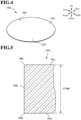
- a disk-shaped glass substrate 100 according to one embodiment of the present invention is a thin plate that has a disk shape and is made of glass, as shown in FIG. 1 showing a perspective view thereof and FIG. 2 showing an enlarged cross-sectional view thereof.
- the disk-shaped glass substrate 100 preferably has a refractive index of 1.60 or more.
- a "thin glass substrate” hereinafter refers to a glass plate having a small plate thickness.
- the disk-shaped glass substrate 100 is an intermediate for cutting out one or more thin glass substrates whose size is smaller than that of the disk-shaped glass substrate 100.
- a cutout thin glass substrate is used as a light-guiding plate, for example, alone, or by combining multiple cutout thin glass substrates as appropriate. If a plurality of cutout thin glass substrates are combined and used as a light-guiding plate, typically, the cutout thin glass substrates are stacked on each other and used as a light-guiding plate.
- a light-guiding body is applied to a display apparatus such as a head-mounted display, for example.
- FIG. 2 is an enlarged view of a cross-section CS1 surrounded by a chain line shown in FIG. 1 when viewed from a front side shown in FIG. 1 .
- the cross-section CS1 is a plane extending in an up-down direction and a right-left direction, and is a cross-section extending in the diameter direction of the main surfaces 101a and 101b. Because the cross-section CS1 shown in FIG. 2 is extremely thin, the cross-section CS1 surrounded by the chain line appears as a substantially thick straight line.
- the two main surfaces 101a and 101b are substantially circular flat surfaces that are arranged side-by-side in the up-down direction.
- the diameter of each of the two main surfaces 101a and 101b is 70 [mm (millimeters)] to 210 [mm], for example.
- the length between the two main surfaces 101a and 101b in the up-down direction that is, the substrate thickness of the disk-shaped glass substrate 100, excluding the outer circumferential edge surface 102a and the chamfering surfaces 103a and 103b, is 50 [ ⁇ m (micrometers)] to 500 [ ⁇ m], for example.
- the substrate thickness of the disk-shaped glass substrate 100, excluding the outer circumferential edge surface 102a and the chamfering surfaces 103a and 103b is preferably 100 [ ⁇ m] to 400 [ ⁇ m], and more preferably 100 [ ⁇ m] to 350 [ ⁇ m].
- the parallelism between the two main surfaces 101a and 101b is less than 1.0 [ ⁇ m], for example, preferably 0.95 [ ⁇ m] or less, and more preferably 0.5 [ ⁇ m] or less.
- the parallelism between the two main surfaces 101a and 101b may be 0.05 [ ⁇ m] or more.
- the "parallelism” refers to a so-called value called TTV (Total Thickness Variation), and indicates the difference between the maximum value and the minimum value of the length of the entire disk-shaped glass substrate 100 measured in the substrate thickness direction (the up-down direction in this embodiment) using one of the main surfaces 101a and 101b as a reference plane.
- TTV Total Thickness Variation
- the roughness (root mean square roughness) Rq of the two main surfaces 101a and 101b is 0.4 [nm] or less, for example.
- the outer circumferential edge surface 102a is a surface forming an end of the disk-shaped glass substrate 100 in the radial direction thereof, and is a curved surface that slightly extends substantially in the up-down direction.
- the outer circumferential edge surface 102a has a substantially circular shape when viewed from above or below, and has an extremely elongated rectangular shape that is short in the up-down direction when viewed from a side.
- a "side" indicates a direction perpendicular to the up-down direction.
- the chamfering surfaces 103a and 103b are surfaces that are respectively inclined between the two main surfaces 101a and 101b and the outer circumferential edge surface 102a and that respectively connect the two main surfaces 101a and 101b and the outer circumferential edge surface 102a, and each have an annular shape when viewed from above or below. That is, the upper chamfering surface 103a is an annular surface that is inclined between an outer edge portion 104a of the upper main surface 101a and an upper end portion 105a of the outer circumferential edge surface 102a and that connects the outer edge portion 104a and the upper end portion 105a.
- the lower chamfering surface 103b is an annular surface that is inclined between an outer edge portion 104b of the lower main surface 101b and a lower end portion 106a of the outer circumferential edge surface 102a and that connects the outer edge portion 104b and the upper end portion 106a.
- the chamfering surfaces 103a and 103b each form a straight line when viewed from a side in this embodiment (see FIG. 2 ). Also, as described above, the chamfering surfaces 103a and 103b are "inclined", and thus intersect the outer circumferential edge surface 102a and intersect the two main surfaces 101a and 101b.
- the chamfering surfaces 103a and 103b according to this embodiment intersect the outer circumferential edge surface 102a and respectively intersect the two main surfaces 101a and 101b at obtuse angles with respect thereto (see FIG. 2 ). Note that the chamfering surfaces 103a and 103b may each form a curved line when viewed from a side.
- the disk-shaped glass substrate 100 is an intermediate for cutting out one or more thin glass substrates.
- the disk-shaped glass substrate 100 has high surface quality and a highly precise substrate thickness, whereby a portion excluding the outer circumferential edge surface 102a and the chamfering surfaces 103a and 103b has a substrate thickness of 100 [ ⁇ m] to 350 [ ⁇ m], and the parallelism between the two main surfaces 101a and 101b is less than 1.0 [ ⁇ m].
- the disk-shaped glass substrate 100 is provided with the chamfering surfaces 103a and 103b.
- the disk-shaped glass substrate 100 is unlikely to be damaged when a thin glass substrate is cut out, and it is possible to cut out thin glass substrates at a yield higher than in a case where no chamfering surfaces 103a and 103b are provided.
- the disk-shaped glass substrate 100 is not only provided with the chamfering surfaces 103a and 103b but also has a disk shape, and thus, as will be described later in detail, even relatively large and thin glass substrates having high surface quality and a highly precise substrate thickness can be stably manufactured at a high yield.
- the disk-shaped glass substrate 100 may have a refractive index of 1.60 or more, and the parallelism between the two main surfaces 101a and 101b may be 0.5 [ ⁇ m] or less. Accordingly, due to the same reasons as above, it is possible to stably mass produce thin glass substrates having high surface quality, a highly precise substrate thickness, and a desired shape.
- a thin glass substrate that is cut out from the disk-shaped glass substrate 100 may be used alone as a light-guiding plate, or a plurality of thin glass substrates that are cut out therefrom may be combined together using a method such as stacking and the combined substrate may be used as a light-guiding plate, for example. Accordingly, due to the same reasons as above, it is possible to stably mass produce light-guiding plates having high surface quality, a highly precise substrate thickness, and a desired shape.
- the method for manufacturing the disk-shaped glass substrate 100 is a method for manufacturing the disk-shaped glass substrate 100 and includes processes shown in the flowchart shown in FIG. 3 , for example.
- a disk-shaped glass blank 107a is prepared (step S1).
- the disk-shaped glass blank 107a is a glass blank that has a disk shape and whose substrate thickness is larger than that of the disk-shaped glass substrate 100 manufactured as an intermediate.
- the disk-shaped glass blank 107a has a substrate thickness t1 of 0.5 [mm] to 1.0 [mm], for example.
- the disk-shaped glass blank 107a preferably has a refractive index of 1.60 or more. The accuracy of the substrate thickness and the surface quality of main surfaces 101c and 101d may be lower than those of the disk-shaped glass substrate 100.
- the disk-shaped glass blank 107a has two main surfaces 101c and 101d, and an outer circumferential edge surface 102b, as shown in FIG. 4 showing a perspective view thereof and FIG. 5 showing an enlarged cross-sectional view thereof.
- FIG. 5 is an enlarged view of a cross-section CS2 surrounded by the chain line shown in FIG. 4 when viewed from a front side shown in FIG. 4 .
- the cross-section CS2 corresponds to the cross-section CS1 shown in FIG. 1 , is a plane extending in the up-down direction and the right-left direction, and extends in the diameter direction of the main surfaces 101c and 101d. Because the cross-section CS2 shown in FIG. 4 is extremely thin, the cross-section CS2 surrounded by the chain line appears as a substantially thick straight line in a manner similar to that for the cross-section CS1 shown in FIG. 1 .
- Such a disk-shaped glass blank 107a is preferably manufactured through appropriate forming processing.
- the disk-shaped glass blank 107a may be manufactured by cutting out a piece of round columnar glass from a prismatic glass mass formed of highly refractive glass and slicing the round columnar glass into a disk shape, for example. Also, the disk-shaped glass blank 107a may be manufactured by cutting a large glass plate formed using a float method or a downdraw method to a predetermined size, for example. Also, the disk-shaped glass blank 107a may be manufactured by press-molding molten glass, using a pair of molds, for example.
- chamfering need not be performed on the outer edge portions 104c and 104d forming outer edges of the main surfaces 101c and 101 d of the disk-shaped glass blank 107a. That is, the main surfaces 101c and 101d of the disk-shaped glass blank 107a and the outer circumferential edge surface 102b intersect respectively at the outer edge portions 104c and 104d.
- the outer edge portions 104c and 104d are respectively substantially linear boundary portions between the main surfaces 101c and 101d of the disk-shaped glass blank 107a and the outer circumferential edge surface 102b, and each form a ridge.
- the main surfaces 101c and 101d and the outer circumferential edge surface 102b intersect at substantially a right angle, when viewed from a side (see FIG. 5 ).
- main surfaces 101c and 101 d are curved or the outer circumferential edge surface 102b is curved in the up-down direction, when viewed from a side, for example, and thus the main surfaces 101c and 101d and the outer circumferential edge surface 102b intersect at a right angle.
- step S2 Chamfering is performed on the disk-shaped glass blank 107a (step S2).
- step S2 the outer edge portions 104c and 104d of the two main surfaces 101c and 101d of the disk-shaped glass blank 107a are chamfered.
- the outer edge portions 104c and 104d which are the boundaries between the main surfaces 101c and 101d of the disk-shaped glass blank 107a and the outer circumferential edge surface 102b, are removed as a result of the chamfering process (step S2) being performed.
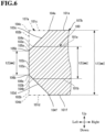
- step S2 As shown in FIG. 6 showing an enlarged cross-sectional view thereof, chamfering surfaces 103c and 103d that connect main surfaces 101e and 101f of a disk-shaped glass blank 107b and an outer circumferential edge surface 102c are formed on the disk-shaped glass blank 107b.
- the upper chamfering surface 103c is an annular surface that is inclined between an outer edge portion 104e of the upper main surface 101 e and an upper end portion 105b of the outer circumferential edge surface 102c and that connects the outer edge portion 104e and the upper end portion 105b.
- the lower chamfering surface 103d is an annular surface that is inclined between an outer edge portion 104f of the lower main surface 101d and a lower end portion 106b of the outer circumferential edge surface 102c and that connects the outer edge portion 104f and the lower end portion 106b.
- the chamfering surfaces 103c and 103d forming straight lines when viewed from a side are formed on the disk-shaped glass blank 107b.
- Such a chamfering process is performed through mechanical processing such as grinding using a grindstone, for example.
- a grinding surface of the grindstone is preferably set to have an inclination angle of 30 to 60 degrees, and more preferably 45 degrees, with respect to each of the two main surfaces 101c and 101d. Accordingly, angles formed between the main surfaces 101e and 101f and the chamfering surfaces 103c and 103d when viewed from a side, and angles formed between the outer circumferential edge surface 102c and the chamfering surfaces 103c and 103d when viewed from a side are formed to be an obtuse angle of 120 to 150 degrees, and more preferably an obtuse angle of 135 degrees.
- FIG. 6 is an enlarged diagram showing a cross-section of the disk-shaped glass blank 107b on which the chamfering process (step S2) has been performed, that is, a cross-section of the chamfered disk-shaped glass blank 107b in the vicinity of the left end thereof when viewed from a front side.
- the cross-section is a plane that extends in the up-down direction and the right-left direction, and is a cross-section that extends in the diameter direction of the main surfaces 101e and 101f.
- the enlarged cross-section of the disk-shaped glass blank 107b is indicated by a solid line.
- an enlarged cross-sectional view (corresponding to the enlarged cross-sectional view shown in FIG. 5 ) of the disk-shaped glass blank 107a that was prepared in step S1 and that has not undergone chamfering is indicated by a chain line.
- the enlarged cross-sectional view (corresponding to the enlarged cross-sectional view shown in FIG. 2 ) of the disk-shaped glass substrate 100 manufactured as an intermediate is indicated by a dotted line.
- FIG. 6 the enlarged views of the disk-shaped glass blanks 107a and 107b and the disk-shaped glass substrate 100 shown in FIG. 6 indicate the cross-sections thereof when viewing, from a front side, substantially the same position and range of the disk-shaped glass blanks 107a and 107b, and the disk-shaped glass substrate 100 overall. That is, FIG.
- FIG. 6 is a diagram showing enlarged cross-sections in a case where the disk-shaped glass blanks 107a and 107b and the disk-shaped glass substrate 100 are disposed such that planes passing through the centers in the up-down direction of the disk-shaped glass blanks 107a and 107b and the disk-shaped glass substrate 100 overlap each other, and the centers of the main surfaces 101a to 101f when viewed in the up-down direction coincide with each other, and the corresponding portions of the disk-shaped glass blanks 107a and 107b and the disk-shaped glass substrate 100 are viewed from a front side.
- the diameters of the main surfaces 101e and 101f of the disk-shaped glass blank 107b and the length of the outer circumferential edge surface 102c in the up-down direction are respectively shorter than the diameters of the main surfaces 101c and 101d of the disk-shaped glass blank 107a prepared in step S1 and the length of the outer circumferential edge surface 102b in the up-down direction as a result of the chamfering process (step S2).
- the outer circumferential edge surface 102c of the disk-shaped glass blank 107b and the upper end portion 105b and the lower end portion 106b thereof respectively substantially coincide with the outer circumferential edge surface 102a of the disk-shaped glass substrate 100, which is an intermediate, and the upper end portion 105a and the lower end portion 106a thereof.
- portions of the upper and lower chamfering surfaces 103c and 103d of the disk-shaped glass blank 107b respectively substantially coincide with the upper and lower chamfering surfaces 103a and 103b of the disk-shaped glass substrate 100, which is an intermediate.
- step S3 Grinding is performed on the two main surfaces 101e and 101f of the chamfered disk-shaped glass blank 107b (step S3).
- the grinding process (step S3) is performed mainly in order to adjust the thickness of the disk-shaped glass blank 107b, and adjust the flatness of the two main surfaces 101e and 101f of the disk-shaped glass blank 107b and parallelism therebetween.
- the machining allowance of the grinding process (step S3) is about 120 [ ⁇ m] to 400 [ ⁇ m], for example.
- the "machining allowance” refers to the length of a portion in the up-down direction to be removed in this process.
- step S3 the two main surfaces 101e and 101f of the chamfered disk-shaped glass blank 107b are ground using a double-side grinding apparatus 108 shown in FIG. 7 simultaneously.
- FIG. 7 shows a configuration of the double-side grinding apparatus 108.
- a method for grinding the main surfaces 101e and 101f of the disk-shaped glass blank 107b in the grinding process (step S3) will be described with reference to FIG. 7 .
- the double-side grinding apparatus 108 has a lower surface plate 109, an upper surface plate 110, an internal gear 111, a sun gear 112, and substantially disk-shaped carriers 113 provided with holding holes.
- a diamond sheet (not shown) is planarly attached to an upper surface of the lower surface plate 109 and a lower surface of the upper surface plate 110.
- the surface of the diamond sheet serves as a grinding surface.
- Fixed abrasive particles have a particle size of about 10 [ ⁇ m], for example.
- the internal gear 111 is a substantially hollow annular member provided with a tooth profile on the inner surface thereof.
- the sun gear 112 is a substantially round columnar member disposed at the center of the internal gear 111, and is provided with a tooth profile on the outer circumferential surface thereof.
- the carriers 113 are holding members for holding the disk-shaped glass blanks 107b in holding holes. Specifically, as shown in FIG. 7 , the disk-shaped glass blanks 107b are held by the carriers 113 as a result of the outer circumferential edge surfaces 102c thereof being housed in the holding holes of the carriers 113 to be in substantially tight contact with wall surfaces forming the holding holes.
- the outer circumferential surfaces of the carriers 113 are provided with teeth.
- the carriers 113 for holding the disk-shaped glass blanks 107b are disposed such that the teeth of the carriers 113 engage with the teeth of the internal gear 111 and the sun gear 112 therebetween.
- FIG. 7 shows an example in which four carriers 113 are disposed between the internal gear 111 and the sun gear 112.
- the number of carriers 113 disposed in the double-side grinding apparatus 108 is not limited to four, and may be 1, 2, 3, 5 or more. Also, the number of disk-shaped glass blanks 107b held by one carrier 113 is not limited to 1, and may be two or more.
- the disk-shaped glass blanks 107b held by the carriers 113 are sandwiched between the lower surface plate 109 and the upper surface plate 110 at a predetermined pressure. Then, either one or both of the upper surface plate 110 and the lower surface plate 109 perform a moving operation. Accordingly, the disk-shaped glass blanks 107b and the surface plates 109 and 110 move relative to each other, and the two main surfaces 101e and 101f of each disk-shaped glass blank 107b are ground simultaneously by fixed abrasive particles included in the above-described diamond sheet.
- the disk-shaped glass blanks 107b can be ground using the same method as in the case of using the above-described fixed abrasive particles using grinding pads instead of the above-described diamond sheet and a grinding slurry containing loose abrasive particles instead of fixed abrasive particles.
- Polishing is performed on two main surfaces of the disk-shaped glass blank (not shown) on which the grinding process (step S3) has been performed, that is, the ground disk-shaped glass blank (step S4).
- the polishing process (step S4) is performed in order to remove blemishes and warping that occur in the grinding, and mirror-polish the glass blank.
- the machining allowance of the polishing process is about 10 [ ⁇ m] to 150 [ ⁇ m], for example, and preferably 20 [ ⁇ m] to 150 [ ⁇ m].
- the polishing process (step S4) is desired to be performed in multiple stages as will be described later as well, and the disk-shaped glass substrate 100 described above with reference to FIGS. 1 and 2 is preferably produced thereby, for example.
- step S4 polishing is performed on two main surfaces of the ground disk-shaped glass blank, using the double-side polishing apparatus, simultaneously, for example.
- the double-side polishing apparatus may have a configuration that is substantially the same as that of the above-described double-side grinding apparatus 108, except that polishing pads are attached to the upper surface of the lower surface plate 109 and the lower surface of the upper surface plate 110, instead of the diamond sheet.
- the polishing pads are flat plate members having an annular shape overall, and are resin polishers, for example. Also, a polishing slurry containing loose abrasive particles is used in the polishing process (step S4).
- step S4 constituent elements of the double-side polishing apparatus utilized in this process (step S4) are given reference numerals of the corresponding constituent elements of the double-side grinding apparatus 108 shown in FIG. 7 .
- the carriers 113 hold the ground disk-shaped glass blanks in a manner similar to that of the above-described double-side grinding apparatus 108.
- the carriers 113 for holding the ground disk-shaped glass blanks are disposed such that the teeth of the carriers 113 engage with the teeth of the internal gear 111 and the sun gear 112 therebetween.
- the disk-shaped glass blanks held by the carriers 113 are sandwiched at a predetermined pressure between the lower surface plate 109 and the upper surface plate 110 provided with the polishing pads. Then, either one or both of the upper surface plate 110 and the lower surface plate 109 performs a moving operation while the polishing slurry is supplied. Accordingly, the ground disk-shaped glass blank and the surface plates 109 and 110 move relative to each other, and the two main surfaces of each disk-shaped glass blank are polished by loose abrasive particles included in the polishing slurry simultaneously.
- the polishing process (step S4) includes a first polishing process (step S41) and a second polishing process (step S42).
- the first polishing process (step S41) is performed mainly in order to remove blemishes and warping remaining on the ground main surfaces, or adjust minute unevenness (microwaviness, roughness, and the like) of the ground main surfaces.
- polishing is performed using the double-side polishing apparatus on the two main surfaces of the disk-shaped glass blank on which the grinding process (step S3) has been performed.
- the machining allowance of the first polishing process (step S41) is about 10 [ ⁇ m] to 100 [ ⁇ m], for example.
- a polishing slurry containing, as loose abrasive particles, cerium oxide abrasive particles, zirconia abrasive particles, or the like having a particle diameter of about 1 [ ⁇ m] to 2 [ ⁇ m] is used, for example.
- step S41 it is preferable to perform polishing in multiple stages with at least one of the polishing pads and the polishing slurry being changed. That is, in this case, a combination of the polishing slurry and the polishing pads applied to the double-side polishing apparatus is preferably changed in the stages of the first polishing process (step S41).
- the parallelism of the disk-shaped glass blank can be adjusted in a range of 0.05 [ ⁇ m] to 0.95 [ ⁇ m] by performing the first polishing process (step S41) in multiple stages in this manner, and as a result, a disk-shaped glass substrate 100 having high surface quality and a highly precise substrate thickness can be obtained.
- the second polishing process (step S42) is performed mainly in order to mirror-polish the main surfaces and reduce roughness thereof.
- polishing is performed using the double-side polishing apparatus on the two main surfaces of the disk-shaped glass blank on which the first polishing process (step S41) has been performed.
- the machining allowance of the second polishing process (step S42) is about 1 [ ⁇ m], for example.
- the second polishing process (step S42) differs from the first polishing process (step S41) in the type and particle size of loose abrasive particles included in the polishing slurry, and the hardness of the resin polishers.
- microparticles having a particle diameter of about 10 [nm (nanometers)] to 50 [nm], such as colloidal silica suspended in a slurry, are used as loose abrasive particles, for example.
- the second polishing process (step S42) differs from the first polishing process (step S41) in at least one of the type and particle size of loose abrasive particles included in the polishing slurry, and the polishing pads. That is, it is preferable that a combination of the polishing slurry and the hardness of the resin polishers applied to the double-side polishing apparatus differs between the first polishing process (step S41) and the second polishing process (step S42).
- the roughness (root mean square roughness) Rq of the main surfaces can be set to 0.4 [nm] by carrying out the second polishing process (step S42).
- the disk-shaped glass substrate 100 having high surface quality can be produced, and thus a thin glass substrate having high surface quality can be produced by being cut out from the disk-shaped glass substrate 100.
- the disk-shaped glass substrate 100 having a highly precise substrate thickness as that shown in FIG. 1 can be produced by performing grinding processing (step S3) and polishing processing (Step S4) on the two main surfaces 101e and 101f of the disk-shaped glass blank 107b.
- the disk-shaped glass substrate 100 to be produced has a substrate thickness t3 of 50 [ ⁇ m] to 500 [ ⁇ m], preferably 100 [ ⁇ m] to 400 [ ⁇ m], and more preferably 100 [ ⁇ m] to 350 [ ⁇ m] in portions excluding the outer circumferential edge surface 102a and the chamfering surfaces 103a and 103b.
- the disk-shaped glass substrate 100 to be produced may have a large diameter of 70 to 210 [mm]. Also, the disk-shaped glass substrate 100 to be produced has high surface quality whereby the parallelism between the two main surfaces 101a and 101b thereof is less than 1.0 [ ⁇ m], and the parallelism therebetween is preferably 0.95 [ ⁇ m] or less, and more preferably 0.5 [ ⁇ m] or less. The parallelism between the two main surfaces 101a and 101b of the disk-shaped glass substrate 100 may be 0.05 [ ⁇ m] or more.
- step S3 the main surfaces of the disk-shaped glass blank are ground and polished with a machining allowance in a range in which at least portions of the chamfering surfaces 103c and 103d formed in the chamfering process (step S2) remain after the processes of step S3 and S4 are performed. Accordingly, the chamfering surfaces 103a and 103b can be reliably provided on the disk-shaped glass substrate 100 to be produced through polishing (step S4).
- the substrate thickness of the chamfered disk-shaped glass blank 107b at the outer circumferential edge surface 102c is t2 [mm]
- the following equation (2) is satisfied.
- the disk-shaped glass substrate 100 is cleaned using a neutral detergent, pure water, IPA (isopropyl alcohol), or the like. Accordingly, the disk-shaped glass substrate 100 shown in FIG. 1 is complete. Note that the shape and size of the disk-shaped glass substrate 100, such as the substrate thickness of the disk-shaped glass substrate 100, usually do not substantially change before and after the cleaning processing (step S5).
- the method for manufacturing the disk-shaped glass substrate 100 according to this embodiment includes the chamfering process (step S2). Damage to the disk-shaped glass blank due to cracks or the like can be suppressed during the subsequent processing processes (steps S3 to S5) or before and after each of the processing processes (steps S3 to S5).
- the grinding process (step S3) and the polishing process (step S4) are performed after the chamfering process (step S2) and objects to be ground and polished have a disk shape, and thus no corner portions are provided. Accordingly, a frictional force applied to the main surfaces 101e and 101f of the disk-shaped glass blank 107b is likely to be uniform in steps S3 and S4. As a result, the disk-shaped glass blank 107b can be processed to have high surface quality and be thin with high accuracy.
- the disk-shaped glass substrate 100 having high surface quality and a highly precise substrate thickness as described above with reference to FIGS. 1 and 2 . That is, the disk-shaped glass substrate 100 has a uniform substrate thickness and uniform and high surface quality, and thus a thin glass substrate having high surface quality and a highly precise substrate thickness, and a desired shape or size can be cut out.
- the chamfering surfaces 103a and 103b are also formed on the produced disk-shaped glass substrate 100 due to the chamfering process (step S2) being included. Accordingly, the disk-shaped glass substrate 100 is unlikely to be damaged when a thin glass substrate is cut out from the disk-shaped glass substrate 100, and it is possible to cut out thin glass substrates at a higher yield than in a case where no chamfering surfaces 103a and 103b are provided.
- the grinding process (step S3) and the polishing process (step S4) are performed after the chamfering process (step S2) and objects to be ground and polished have a disk shape, and thus no corner portions are provided.
- the disk-shaped glass substrates 100 having a large diameter of 70 to 210 mm, and having high surface quality and a highly precise substrate thickness.
- more thin glass substrates can be cut out from a large disk-shaped glass substrate 100 than from a small disk-shaped glass substrate 100.
- stable mass production of thin glass substrates having high surface quality and a highly precise substrate thickness can be facilitated by cutting out thin glass substrates from a large disk-shaped glass substrate 100.
- the method for manufacturing the thin glass substrate 114 according to this embodiment is a method for manufacturing a plurality of thin glass substrates 114 from the disk-shaped glass substrate 100, which is an intermediate, and includes processes shown in the flowchart shown in FIG. 8 , for example.
- step S6 a plurality of rectangular thin glass substrates 114 are cut out from the disk-shaped glass substrate 100.
- the cut-out processing is performed on the disk-shaped glass substrate 100 manufactured using the method for manufacturing the disk-shaped glass substrate 100.
- the disk-shaped glass substrate 100 is cut along dotted straight lines shown in FIG. 9 . Accordingly, a plurality of rectangular thin glass substrates 114 as shown in an enlarged manner in FIG. 9 are cut out from the disk-shaped glass substrate 100.
- the disk-shaped glass substrate 100 having a uniform substrate thickness and uniform and high surface quality can be produced through the processes of steps S1 to S5.
- a plurality of thin glass substrates 114 having high surface quality and a highly precise substrate thickness can be obtained regardless of portions from which the thin glass substrates 114 are cut out.
- the thin glass substrate 114 having high surface quality and a highly precise substrate thickness can be obtained.
- the disk-shaped glass substrate 100 is unlikely to be damaged when the thin glass substrates 114 are cut out from the disk-shaped glass substrate 100 due to this method including the chamfering process (step S2).
- this method including the chamfering process (step S2).
- rectangular thin glass substrates 114 having corner portions as described as an example here can be obtained at a higher yield than in a case where no chamfering surfaces 103a and 103b are provided.
- the number of thin glass substrates 114 to be cut out from the disk-shaped glass substrate 100 may be one.
- the shapes and sizes of one or more thin glass substrates 114 that are cut out from the disk-shaped glass substrate 100 may be changed as appropriate, and the thin glass substrates 114 may have a shape having no corner portions, for example. Accordingly, it is possible to stably mass produce thin glass substrates 114 having high surface quality, a highly precise substrate thickness, and a desired shape.
- a single thin glass substrate 114 manufactured using the method for manufacturing the thin glass substrate 114 described here may be utilized as a light-guiding plate.
- the method for manufacturing the thin glass substrate 114 described here is preferably adopted as a method for manufacturing a light-guiding plate. Accordingly, it is possible to stably mass produce light-guiding plates having high surface quality, a highly precise substrate thickness, and a desired shape.
- the method for manufacturing the light-guiding plate 115 is a method for manufacturing the light-guiding plate 115 by combining a plurality of thin glass substrates 114, and includes processes shown in the flowchart shown in FIG. 10 , for example.
- step S7 the stacking process (step S7) is performed on the thin glass substrates 114 manufactured using the method for manufacturing the thin glass substrate 114.
- steps S1 to S6 in the method for manufacturing the thin glass substrate 114 are not shown in FIG. 10 . That is, steps S1 to S5 in the method for manufacturing the light-guiding plate 115 may respectively be the same as steps S1 to S5 in the method for manufacturing the disk-shaped glass substrate 100.
- step S7 the thin glass substrates 114 are stacked on each other in the up-down direction with adjacent thin glass substrates 114 being fixed to each other, and thus the light-guiding plate 115 as shown in FIG. 11 is produced.
- step S7 the number of thin glass substrates 114 to be stacked in the stacking process may be determined as appropriate.
- the light-guiding plate 115 can be produced by cutting out a plurality of thin glass substrates 114 having high surface quality and a highly precise substrate thickness and stacking the cutout thin glass substrates 114 on each other. As described above, it is possible to stably mass produce thin glass substrates 114 having high surface quality, a highly precise substrate thickness, and corner portions. Thus, it is possible to stably mass produce light-guiding plates 115 having high surface quality, a highly precise substrate thickness, and corner portions.
- thin glass substrates 114 to be cut out from the disk-shaped glass substrate 100 in the cut-out processing may have a desired shape and size. Accordingly, it is possible to stably mass produce light-guiding plates 115 having high surface quality, a highly precise substrate thickness, and a desired shape.
- the present invention can be utilized for mass production of glass substrates with high surface quality and a small substrate thickness, such as glass substrates to be applied to display apparatuses such as head-mounted displays.
Landscapes
- Engineering & Computer Science (AREA)
- Mechanical Engineering (AREA)
- Chemical & Material Sciences (AREA)
- Inorganic Chemistry (AREA)
- Ceramic Engineering (AREA)
- Physics & Mathematics (AREA)
- Optics & Photonics (AREA)
- Chemical Kinetics & Catalysis (AREA)
- General Chemical & Material Sciences (AREA)
- Geochemistry & Mineralogy (AREA)
- Materials Engineering (AREA)
- Organic Chemistry (AREA)
- Life Sciences & Earth Sciences (AREA)
- General Physics & Mathematics (AREA)
- Mining & Mineral Resources (AREA)
- Manufacturing Of Magnetic Record Carriers (AREA)
- Grinding And Polishing Of Tertiary Curved Surfaces And Surfaces With Complex Shapes (AREA)
- Surface Treatment Of Glass (AREA)
- Finish Polishing, Edge Sharpening, And Grinding By Specific Grinding Devices (AREA)
Priority Applications (1)
| Application Number | Priority Date | Filing Date | Title |
|---|---|---|---|
| EP23218195.8A EP4368340A1 (en) | 2017-12-27 | 2018-12-20 | Disk-shaped glass substrate manufacturing method, sheet glass substrate manufacturing method, light guide plate manufacturing method, and disk-shaped glass substrate |
Applications Claiming Priority (2)
| Application Number | Priority Date | Filing Date | Title |
|---|---|---|---|
| JP2017251419A JP6695318B2 (ja) | 2017-12-27 | 2017-12-27 | 円盤状ガラス基板の製造方法、薄板ガラス基板の製造方法、導光板の製造方法及び円盤状ガラス基板 |
| PCT/JP2018/046973 WO2019131431A1 (ja) | 2017-12-27 | 2018-12-20 | 円盤状ガラス基板の製造方法、薄板ガラス基板の製造方法、導光板の製造方法及び円盤状ガラス基板 |
Related Child Applications (2)
| Application Number | Title | Priority Date | Filing Date |
|---|---|---|---|
| EP23218195.8A Division EP4368340A1 (en) | 2017-12-27 | 2018-12-20 | Disk-shaped glass substrate manufacturing method, sheet glass substrate manufacturing method, light guide plate manufacturing method, and disk-shaped glass substrate |
| EP23218195.8A Division-Into EP4368340A1 (en) | 2017-12-27 | 2018-12-20 | Disk-shaped glass substrate manufacturing method, sheet glass substrate manufacturing method, light guide plate manufacturing method, and disk-shaped glass substrate |
Publications (3)
| Publication Number | Publication Date |
|---|---|
| EP3670081A1 EP3670081A1 (en) | 2020-06-24 |
| EP3670081A4 EP3670081A4 (en) | 2021-07-14 |
| EP3670081B1 true EP3670081B1 (en) | 2024-09-25 |
Family
ID=67067318
Family Applications (2)
| Application Number | Title | Priority Date | Filing Date |
|---|---|---|---|
| EP18896269.0A Active EP3670081B1 (en) | 2017-12-27 | 2018-12-20 | Disk-shaped glass substrate manufacturing method, glass substrate manufacturing method and light guide plate manufacturing method |
| EP23218195.8A Pending EP4368340A1 (en) | 2017-12-27 | 2018-12-20 | Disk-shaped glass substrate manufacturing method, sheet glass substrate manufacturing method, light guide plate manufacturing method, and disk-shaped glass substrate |
Family Applications After (1)
| Application Number | Title | Priority Date | Filing Date |
|---|---|---|---|
| EP23218195.8A Pending EP4368340A1 (en) | 2017-12-27 | 2018-12-20 | Disk-shaped glass substrate manufacturing method, sheet glass substrate manufacturing method, light guide plate manufacturing method, and disk-shaped glass substrate |
Country Status (5)
| Country | Link |
|---|---|
| US (1) | US20200270174A1 (https=) |
| EP (2) | EP3670081B1 (https=) |
| JP (1) | JP6695318B2 (https=) |
| CN (2) | CN114918743B (https=) |
| WO (1) | WO2019131431A1 (https=) |
Families Citing this family (4)
| Publication number | Priority date | Publication date | Assignee | Title |
|---|---|---|---|---|
| JP7643454B2 (ja) | 2020-04-23 | 2025-03-11 | Agc株式会社 | ガラス物品およびガラス物品の製造方法 |
| US12486197B2 (en) | 2020-09-04 | 2025-12-02 | Schott Ag | Method of surface structuring a substrate body and substrate body |
| CN117182663A (zh) * | 2023-09-01 | 2023-12-08 | 甘肃旭晶新材料有限公司 | 蓝宝石导光块的加工方法及采用该方法制作的产品 |
| CN118636301B (zh) * | 2024-08-16 | 2024-12-13 | 浙江罗克光电科技股份有限公司 | 一种2.5d微晶玻璃的加工工艺及装置 |
Citations (1)
| Publication number | Priority date | Publication date | Assignee | Title |
|---|---|---|---|---|
| US20140033768A1 (en) * | 2011-04-27 | 2014-02-06 | Hoya Corporation | Method for manufacturing glass blank for magnetic disk, method for manufacturing glass substrate for magnetic disk |
Family Cites Families (28)
| Publication number | Priority date | Publication date | Assignee | Title |
|---|---|---|---|---|
| US20020192421A1 (en) * | 2001-05-22 | 2002-12-19 | Jennings Timothy Allan | Composite glassy carbon disk substrate for a data storage device and method for fabricating same |
| WO2006025572A1 (en) * | 2004-08-30 | 2006-03-09 | Showa Denko K.K. | Glass substrate for magnetic recording medium and magnetic recording medium |
| JP4184384B2 (ja) * | 2006-03-16 | 2008-11-19 | Hoya株式会社 | 磁気記録媒体用ガラス基板、及び磁気記録媒体 |
| CN102086095B (zh) * | 2006-03-24 | 2012-11-28 | Hoya株式会社 | 磁盘用玻璃衬底的制造方法以及磁盘的制造方法 |
| US20100007444A1 (en) * | 2006-04-20 | 2010-01-14 | Anis Nurashikin Nordin | GHz Surface Acoustic Resonators in RF-CMOS |
| JP2008216835A (ja) * | 2007-03-07 | 2008-09-18 | Epson Imaging Devices Corp | 薄型基板の製造方法 |
| JP2009035461A (ja) * | 2007-08-03 | 2009-02-19 | Asahi Glass Co Ltd | 磁気ディスク用ガラス基板の製造方法 |
| JP5056961B2 (ja) * | 2010-02-01 | 2012-10-24 | 旭硝子株式会社 | 磁気記録媒体用ガラス基板及びその製造方法 |
| JP5533355B2 (ja) * | 2010-07-01 | 2014-06-25 | 旭硝子株式会社 | 磁気記録媒体用ガラス基板、両面研磨装置、ガラス基板の研磨方法及びガラス基板の製造方法 |
| KR101638488B1 (ko) * | 2010-12-08 | 2016-07-11 | 니폰 덴키 가라스 가부시키가이샤 | 고굴절률 유리 |
| JP5741157B2 (ja) * | 2011-04-07 | 2015-07-01 | 旭硝子株式会社 | 研磨用キャリア及び該キャリアを用いたガラス基板の研磨方法及びガラス基板の製造方法 |
| CN103764585A (zh) * | 2011-08-29 | 2014-04-30 | 旭硝子株式会社 | 玻璃板及玻璃板的制造方法 |
| JP5661950B2 (ja) * | 2011-12-29 | 2015-01-28 | Hoya株式会社 | 磁気ディスク用ガラス基板の製造方法 |
| JP6110364B2 (ja) * | 2012-03-13 | 2017-04-05 | Hoya株式会社 | 電子機器用カバーガラスのガラス基板、及びその製造方法 |
| US9753317B2 (en) * | 2012-12-21 | 2017-09-05 | Apple Inc. | Methods for trimming polarizers in displays using edge protection structures |
| WO2014103986A1 (ja) * | 2012-12-28 | 2014-07-03 | Hoya株式会社 | 情報記録媒体用ガラス基板およびその製造方法 |
| CN105164752B (zh) * | 2013-04-30 | 2018-09-14 | Hoya株式会社 | 磁盘用玻璃基板的制造方法和磁盘的制造方法、以及磁盘用玻璃基板的端面研磨装置 |
| CN103332860B (zh) * | 2013-06-08 | 2015-06-24 | 鄂尔多斯市紫荆创新研究院 | 一种用煤矸石制造建筑装饰用微晶玻璃板材的方法 |
| JP6129029B2 (ja) * | 2013-08-30 | 2017-05-17 | 株式会社ディスコ | ウェーハの加工方法 |
| JP2015064920A (ja) * | 2013-09-25 | 2015-04-09 | Hoya株式会社 | 磁気ディスク用ガラス基板の製造方法 |
| US10442719B2 (en) * | 2013-12-17 | 2019-10-15 | Corning Incorporated | Edge chamfering methods |
| CN107107568A (zh) * | 2014-12-26 | 2017-08-29 | 旭硝子株式会社 | 玻璃层叠体、电子器件的制造方法、玻璃层叠体的制造方法、玻璃板包装体 |
| JP2015181082A (ja) * | 2015-04-28 | 2015-10-15 | 旭硝子株式会社 | 磁気記録媒体用ガラス基板 |
| JP2016224116A (ja) * | 2015-05-27 | 2016-12-28 | シャープ株式会社 | 表示パネルの製造方法 |
| CN106250800B (zh) * | 2015-06-05 | 2021-08-27 | Agc株式会社 | 一种保护玻璃以及便携式信息终端 |
| CN208378728U (zh) * | 2015-06-12 | 2019-01-15 | Agc株式会社 | 玻璃板和显示装置 |
| JP2017032673A (ja) * | 2015-07-30 | 2017-02-09 | 日本電気硝子株式会社 | 導光板及びこれを用いた積層導光板 |
| JP6106813B1 (ja) * | 2015-09-30 | 2017-04-05 | Hoya株式会社 | 磁気ディスク用ガラス基板、磁気ディスク、ガラス基板中間体、及び磁気ディスク用ガラス基板の製造方法 |
-
2017
- 2017-12-27 JP JP2017251419A patent/JP6695318B2/ja active Active
-
2018
- 2018-12-20 CN CN202210574389.5A patent/CN114918743B/zh active Active
- 2018-12-20 WO PCT/JP2018/046973 patent/WO2019131431A1/ja not_active Ceased
- 2018-12-20 EP EP18896269.0A patent/EP3670081B1/en active Active
- 2018-12-20 US US16/645,741 patent/US20200270174A1/en active Pending
- 2018-12-20 EP EP23218195.8A patent/EP4368340A1/en active Pending
- 2018-12-20 CN CN201880066936.0A patent/CN111246971B/zh active Active
Patent Citations (1)
| Publication number | Priority date | Publication date | Assignee | Title |
|---|---|---|---|---|
| US20140033768A1 (en) * | 2011-04-27 | 2014-02-06 | Hoya Corporation | Method for manufacturing glass blank for magnetic disk, method for manufacturing glass substrate for magnetic disk |
Also Published As
| Publication number | Publication date |
|---|---|
| CN111246971B (zh) | 2023-04-04 |
| EP4368340A1 (en) | 2024-05-15 |
| WO2019131431A1 (ja) | 2019-07-04 |
| EP3670081A4 (en) | 2021-07-14 |
| CN114918743A (zh) | 2022-08-19 |
| EP3670081A1 (en) | 2020-06-24 |
| JP6695318B2 (ja) | 2020-05-20 |
| US20200270174A1 (en) | 2020-08-27 |
| CN111246971A (zh) | 2020-06-05 |
| CN114918743B (zh) | 2024-05-31 |
| JP2019115952A (ja) | 2019-07-18 |
Similar Documents
| Publication | Publication Date | Title |
|---|---|---|
| EP3670081B1 (en) | Disk-shaped glass substrate manufacturing method, glass substrate manufacturing method and light guide plate manufacturing method | |
| US8454852B2 (en) | Chamfering apparatus for silicon wafer, method for producing silicon wafer, and etched silicon wafer | |
| JP5472073B2 (ja) | 半導体ウェーハ及びその製造方法 | |
| CN102441828A (zh) | 玻璃板的端缘部研磨方法 | |
| JP2013198974A (ja) | ガラス基板の端面研削装置、ガラス基板の端面研削方法、及びガラス基板の製造方法 | |
| JP6913295B2 (ja) | ガラス板、及びガラス板の製造方法 | |
| JP2020003547A (ja) | フォトマスク用基板およびその製造方法 | |
| US11361959B2 (en) | Method for manufacturing wafer | |
| JP6236191B1 (ja) | キャリアおよび当該キャリアを用いた基板の製造方法 | |
| JP7397844B2 (ja) | 円盤状ガラス基板の製造方法、薄板ガラス基板の製造方法、導光板の製造方法及び円盤状ガラス基板 | |
| CN102016664A (zh) | 制造微尺寸的光学结构的方法 | |
| JP2015069674A (ja) | 磁気ディスク用ガラス基板の製造方法及び研磨処理用キャリア | |
| TW202306698A (zh) | 半導體晶圓的製造方法 | |
| US12266389B2 (en) | Magnetic disk substrate, magnetic disk, annular-shaped substrate, and method for manufacturing magnetic disk substrate | |
| JP7131724B1 (ja) | 半導体ウェーハの製造方法 | |
| JP5212877B2 (ja) | フラットディスプレイ用ガラス基板梱包体 | |
| KR20200009420A (ko) | 반도체용 기판 및 그의 제조 방법 |
Legal Events
| Date | Code | Title | Description |
|---|---|---|---|
| STAA | Information on the status of an ep patent application or granted ep patent |
Free format text: STATUS: THE INTERNATIONAL PUBLICATION HAS BEEN MADE |
|
| PUAI | Public reference made under article 153(3) epc to a published international application that has entered the european phase |
Free format text: ORIGINAL CODE: 0009012 |
|
| STAA | Information on the status of an ep patent application or granted ep patent |
Free format text: STATUS: REQUEST FOR EXAMINATION WAS MADE |
|
| 17P | Request for examination filed |
Effective date: 20200316 |
|
| AK | Designated contracting states |
Kind code of ref document: A1 Designated state(s): AL AT BE BG CH CY CZ DE DK EE ES FI FR GB GR HR HU IE IS IT LI LT LU LV MC MK MT NL NO PL PT RO RS SE SI SK SM TR |
|
| AX | Request for extension of the european patent |
Extension state: BA ME |
|
| DAV | Request for validation of the european patent (deleted) | ||
| DAX | Request for extension of the european patent (deleted) | ||
| A4 | Supplementary search report drawn up and despatched |
Effective date: 20210615 |
|
| RIC1 | Information provided on ipc code assigned before grant |
Ipc: B24B 37/08 20120101AFI20210609BHEP Ipc: B24B 9/00 20060101ALI20210609BHEP Ipc: C03C 19/00 20060101ALI20210609BHEP Ipc: F21V 8/00 20060101ALI20210609BHEP Ipc: B24B 7/24 20060101ALN20210609BHEP |
|
| STAA | Information on the status of an ep patent application or granted ep patent |
Free format text: STATUS: EXAMINATION IS IN PROGRESS |
|
| 17Q | First examination report despatched |
Effective date: 20220516 |
|
| GRAP | Despatch of communication of intention to grant a patent |
Free format text: ORIGINAL CODE: EPIDOSNIGR1 |
|
| STAA | Information on the status of an ep patent application or granted ep patent |
Free format text: STATUS: GRANT OF PATENT IS INTENDED |
|
| RIC1 | Information provided on ipc code assigned before grant |
Ipc: B24B 7/24 20060101ALN20240403BHEP Ipc: F21V 8/00 20060101ALI20240403BHEP Ipc: C03C 19/00 20060101ALI20240403BHEP Ipc: B24B 9/00 20060101ALI20240403BHEP Ipc: B24B 37/08 20120101AFI20240403BHEP |
|
| INTG | Intention to grant announced |
Effective date: 20240417 |
|
| GRAS | Grant fee paid |
Free format text: ORIGINAL CODE: EPIDOSNIGR3 |
|
| GRAA | (expected) grant |
Free format text: ORIGINAL CODE: 0009210 |
|
| STAA | Information on the status of an ep patent application or granted ep patent |
Free format text: STATUS: THE PATENT HAS BEEN GRANTED |
|
| AK | Designated contracting states |
Kind code of ref document: B1 Designated state(s): AL AT BE BG CH CY CZ DE DK EE ES FI FR GB GR HR HU IE IS IT LI LT LU LV MC MK MT NL NO PL PT RO RS SE SI SK SM TR |
|
| P01 | Opt-out of the competence of the unified patent court (upc) registered |
Free format text: CASE NUMBER: APP_47574/2024 Effective date: 20240819 |
|
| REG | Reference to a national code |
Ref country code: GB Ref legal event code: FG4D |
|
| REG | Reference to a national code |
Ref country code: CH Ref legal event code: EP |
|
| REG | Reference to a national code |
Ref country code: DE Ref legal event code: R096 Ref document number: 602018074822 Country of ref document: DE |
|
| REG | Reference to a national code |
Ref country code: IE Ref legal event code: FG4D |
|
| REG | Reference to a national code |
Ref country code: LT Ref legal event code: MG9D |
|
| PG25 | Lapsed in a contracting state [announced via postgrant information from national office to epo] |
Ref country code: NO Free format text: LAPSE BECAUSE OF FAILURE TO SUBMIT A TRANSLATION OF THE DESCRIPTION OR TO PAY THE FEE WITHIN THE PRESCRIBED TIME-LIMIT Effective date: 20241225 |
|
| PG25 | Lapsed in a contracting state [announced via postgrant information from national office to epo] |
Ref country code: GR Free format text: LAPSE BECAUSE OF FAILURE TO SUBMIT A TRANSLATION OF THE DESCRIPTION OR TO PAY THE FEE WITHIN THE PRESCRIBED TIME-LIMIT Effective date: 20241226 Ref country code: FI Free format text: LAPSE BECAUSE OF FAILURE TO SUBMIT A TRANSLATION OF THE DESCRIPTION OR TO PAY THE FEE WITHIN THE PRESCRIBED TIME-LIMIT Effective date: 20240925 |
|
| PG25 | Lapsed in a contracting state [announced via postgrant information from national office to epo] |
Ref country code: BG Free format text: LAPSE BECAUSE OF FAILURE TO SUBMIT A TRANSLATION OF THE DESCRIPTION OR TO PAY THE FEE WITHIN THE PRESCRIBED TIME-LIMIT Effective date: 20240925 |
|
| PG25 | Lapsed in a contracting state [announced via postgrant information from national office to epo] |
Ref country code: LV Free format text: LAPSE BECAUSE OF FAILURE TO SUBMIT A TRANSLATION OF THE DESCRIPTION OR TO PAY THE FEE WITHIN THE PRESCRIBED TIME-LIMIT Effective date: 20240925 |
|
| PG25 | Lapsed in a contracting state [announced via postgrant information from national office to epo] |
Ref country code: RS Free format text: LAPSE BECAUSE OF FAILURE TO SUBMIT A TRANSLATION OF THE DESCRIPTION OR TO PAY THE FEE WITHIN THE PRESCRIBED TIME-LIMIT Effective date: 20241225 |
|
| REG | Reference to a national code |
Ref country code: NL Ref legal event code: MP Effective date: 20240925 |
|
| PG25 | Lapsed in a contracting state [announced via postgrant information from national office to epo] |
Ref country code: RS Free format text: LAPSE BECAUSE OF FAILURE TO SUBMIT A TRANSLATION OF THE DESCRIPTION OR TO PAY THE FEE WITHIN THE PRESCRIBED TIME-LIMIT Effective date: 20241225 Ref country code: NO Free format text: LAPSE BECAUSE OF FAILURE TO SUBMIT A TRANSLATION OF THE DESCRIPTION OR TO PAY THE FEE WITHIN THE PRESCRIBED TIME-LIMIT Effective date: 20241225 Ref country code: LV Free format text: LAPSE BECAUSE OF FAILURE TO SUBMIT A TRANSLATION OF THE DESCRIPTION OR TO PAY THE FEE WITHIN THE PRESCRIBED TIME-LIMIT Effective date: 20240925 Ref country code: GR Free format text: LAPSE BECAUSE OF FAILURE TO SUBMIT A TRANSLATION OF THE DESCRIPTION OR TO PAY THE FEE WITHIN THE PRESCRIBED TIME-LIMIT Effective date: 20241226 Ref country code: FI Free format text: LAPSE BECAUSE OF FAILURE TO SUBMIT A TRANSLATION OF THE DESCRIPTION OR TO PAY THE FEE WITHIN THE PRESCRIBED TIME-LIMIT Effective date: 20240925 Ref country code: BG Free format text: LAPSE BECAUSE OF FAILURE TO SUBMIT A TRANSLATION OF THE DESCRIPTION OR TO PAY THE FEE WITHIN THE PRESCRIBED TIME-LIMIT Effective date: 20240925 |
|
| REG | Reference to a national code |
Ref country code: AT Ref legal event code: MK05 Ref document number: 1726273 Country of ref document: AT Kind code of ref document: T Effective date: 20240925 |
|
| PG25 | Lapsed in a contracting state [announced via postgrant information from national office to epo] |
Ref country code: NL Free format text: LAPSE BECAUSE OF FAILURE TO SUBMIT A TRANSLATION OF THE DESCRIPTION OR TO PAY THE FEE WITHIN THE PRESCRIBED TIME-LIMIT Effective date: 20240925 |
|
| PG25 | Lapsed in a contracting state [announced via postgrant information from national office to epo] |
Ref country code: IS Free format text: LAPSE BECAUSE OF FAILURE TO SUBMIT A TRANSLATION OF THE DESCRIPTION OR TO PAY THE FEE WITHIN THE PRESCRIBED TIME-LIMIT Effective date: 20250125 Ref country code: PT Free format text: LAPSE BECAUSE OF FAILURE TO SUBMIT A TRANSLATION OF THE DESCRIPTION OR TO PAY THE FEE WITHIN THE PRESCRIBED TIME-LIMIT Effective date: 20250127 |
|
| PG25 | Lapsed in a contracting state [announced via postgrant information from national office to epo] |
Ref country code: RO Free format text: LAPSE BECAUSE OF FAILURE TO SUBMIT A TRANSLATION OF THE DESCRIPTION OR TO PAY THE FEE WITHIN THE PRESCRIBED TIME-LIMIT Effective date: 20240925 Ref country code: SM Free format text: LAPSE BECAUSE OF FAILURE TO SUBMIT A TRANSLATION OF THE DESCRIPTION OR TO PAY THE FEE WITHIN THE PRESCRIBED TIME-LIMIT Effective date: 20240925 |
|
| PG25 | Lapsed in a contracting state [announced via postgrant information from national office to epo] |
Ref country code: ES Free format text: LAPSE BECAUSE OF FAILURE TO SUBMIT A TRANSLATION OF THE DESCRIPTION OR TO PAY THE FEE WITHIN THE PRESCRIBED TIME-LIMIT Effective date: 20240925 |
|
| PG25 | Lapsed in a contracting state [announced via postgrant information from national office to epo] |
Ref country code: EE Free format text: LAPSE BECAUSE OF FAILURE TO SUBMIT A TRANSLATION OF THE DESCRIPTION OR TO PAY THE FEE WITHIN THE PRESCRIBED TIME-LIMIT Effective date: 20240925 Ref country code: AT Free format text: LAPSE BECAUSE OF FAILURE TO SUBMIT A TRANSLATION OF THE DESCRIPTION OR TO PAY THE FEE WITHIN THE PRESCRIBED TIME-LIMIT Effective date: 20240925 |
|
| PG25 | Lapsed in a contracting state [announced via postgrant information from national office to epo] |
Ref country code: CZ Free format text: LAPSE BECAUSE OF FAILURE TO SUBMIT A TRANSLATION OF THE DESCRIPTION OR TO PAY THE FEE WITHIN THE PRESCRIBED TIME-LIMIT Effective date: 20240925 Ref country code: PL Free format text: LAPSE BECAUSE OF FAILURE TO SUBMIT A TRANSLATION OF THE DESCRIPTION OR TO PAY THE FEE WITHIN THE PRESCRIBED TIME-LIMIT Effective date: 20240925 |
|
| PG25 | Lapsed in a contracting state [announced via postgrant information from national office to epo] |
Ref country code: SK Free format text: LAPSE BECAUSE OF FAILURE TO SUBMIT A TRANSLATION OF THE DESCRIPTION OR TO PAY THE FEE WITHIN THE PRESCRIBED TIME-LIMIT Effective date: 20240925 Ref country code: IT Free format text: LAPSE BECAUSE OF FAILURE TO SUBMIT A TRANSLATION OF THE DESCRIPTION OR TO PAY THE FEE WITHIN THE PRESCRIBED TIME-LIMIT Effective date: 20240925 |
|
| REG | Reference to a national code |
Ref country code: DE Ref legal event code: R097 Ref document number: 602018074822 Country of ref document: DE |
|
| PG25 | Lapsed in a contracting state [announced via postgrant information from national office to epo] |
Ref country code: MC Free format text: LAPSE BECAUSE OF FAILURE TO SUBMIT A TRANSLATION OF THE DESCRIPTION OR TO PAY THE FEE WITHIN THE PRESCRIBED TIME-LIMIT Effective date: 20240925 |
|
| PG25 | Lapsed in a contracting state [announced via postgrant information from national office to epo] |
Ref country code: DK Free format text: LAPSE BECAUSE OF FAILURE TO SUBMIT A TRANSLATION OF THE DESCRIPTION OR TO PAY THE FEE WITHIN THE PRESCRIBED TIME-LIMIT Effective date: 20240925 |
|
| REG | Reference to a national code |
Ref country code: CH Ref legal event code: PL |
|
| PLBE | No opposition filed within time limit |
Free format text: ORIGINAL CODE: 0009261 |
|
| STAA | Information on the status of an ep patent application or granted ep patent |
Free format text: STATUS: NO OPPOSITION FILED WITHIN TIME LIMIT |
|
| PG25 | Lapsed in a contracting state [announced via postgrant information from national office to epo] |
Ref country code: LU Free format text: LAPSE BECAUSE OF NON-PAYMENT OF DUE FEES Effective date: 20241220 |
|
| GBPC | Gb: european patent ceased through non-payment of renewal fee |
Effective date: 20241225 |
|
| 26N | No opposition filed |
Effective date: 20250626 |
|
| PG25 | Lapsed in a contracting state [announced via postgrant information from national office to epo] |
Ref country code: SE Free format text: LAPSE BECAUSE OF FAILURE TO SUBMIT A TRANSLATION OF THE DESCRIPTION OR TO PAY THE FEE WITHIN THE PRESCRIBED TIME-LIMIT Effective date: 20240925 |
|
| REG | Reference to a national code |
Ref country code: BE Ref legal event code: MM Effective date: 20241231 |
|
| PG25 | Lapsed in a contracting state [announced via postgrant information from national office to epo] |
Ref country code: GB Free format text: LAPSE BECAUSE OF NON-PAYMENT OF DUE FEES Effective date: 20241225 Ref country code: BE Free format text: LAPSE BECAUSE OF NON-PAYMENT OF DUE FEES Effective date: 20241231 |
|
| PG25 | Lapsed in a contracting state [announced via postgrant information from national office to epo] |
Ref country code: FR Free format text: LAPSE BECAUSE OF NON-PAYMENT OF DUE FEES Effective date: 20241231 |
|
| PG25 | Lapsed in a contracting state [announced via postgrant information from national office to epo] |
Ref country code: CH Free format text: LAPSE BECAUSE OF NON-PAYMENT OF DUE FEES Effective date: 20241231 |
|
| PG25 | Lapsed in a contracting state [announced via postgrant information from national office to epo] |
Ref country code: IE Free format text: LAPSE BECAUSE OF NON-PAYMENT OF DUE FEES Effective date: 20241220 |
|
| PGFP | Annual fee paid to national office [announced via postgrant information from national office to epo] |
Ref country code: DE Payment date: 20251028 Year of fee payment: 8 |
|
| PG25 | Lapsed in a contracting state [announced via postgrant information from national office to epo] |
Ref country code: HR Free format text: LAPSE BECAUSE OF FAILURE TO SUBMIT A TRANSLATION OF THE DESCRIPTION OR TO PAY THE FEE WITHIN THE PRESCRIBED TIME-LIMIT Effective date: 20240925 |