EP3663892B1 - Speichermodul mit bildschirm und hauptplatinenmodul - Google Patents
Speichermodul mit bildschirm und hauptplatinenmodul Download PDFInfo
- Publication number
- EP3663892B1 EP3663892B1 EP19204446.9A EP19204446A EP3663892B1 EP 3663892 B1 EP3663892 B1 EP 3663892B1 EP 19204446 A EP19204446 A EP 19204446A EP 3663892 B1 EP3663892 B1 EP 3663892B1
- Authority
- EP
- European Patent Office
- Prior art keywords
- memory
- screen
- module
- power conversion
- disposed
- Prior art date
- Legal status (The legal status is an assumption and is not a legal conclusion. Google has not performed a legal analysis and makes no representation as to the accuracy of the status listed.)
- Active
Links
Images




Classifications
-
- G—PHYSICS
- G06—COMPUTING OR CALCULATING; COUNTING
- G06F—ELECTRIC DIGITAL DATA PROCESSING
- G06F1/00—Details not covered by groups G06F3/00 - G06F13/00 and G06F21/00
- G06F1/16—Constructional details or arrangements
- G06F1/18—Packaging or power distribution
- G06F1/183—Internal mounting support structures, e.g. for supporting printed circuit boards
-
- G—PHYSICS
- G11—INFORMATION STORAGE
- G11C—STATIC STORES
- G11C5/00—Details of stores covered by group G11C11/00
- G11C5/02—Disposition of storage elements, e.g. in the form of a matrix array
- G11C5/04—Supports for storage elements, e.g. memory modules; Mounting or fixing of storage elements on such supports
-
- G—PHYSICS
- G06—COMPUTING OR CALCULATING; COUNTING
- G06F—ELECTRIC DIGITAL DATA PROCESSING
- G06F1/00—Details not covered by groups G06F3/00 - G06F13/00 and G06F21/00
- G06F1/16—Constructional details or arrangements
- G06F1/1601—Constructional details related to the housing of computer displays, e.g. of CRT monitors, of flat displays
-
- G—PHYSICS
- G06—COMPUTING OR CALCULATING; COUNTING
- G06F—ELECTRIC DIGITAL DATA PROCESSING
- G06F1/00—Details not covered by groups G06F3/00 - G06F13/00 and G06F21/00
- G06F1/16—Constructional details or arrangements
- G06F1/18—Packaging or power distribution
- G06F1/183—Internal mounting support structures, e.g. for supporting printed circuit boards
- G06F1/185—Mounting of expansion boards
-
- G—PHYSICS
- G06—COMPUTING OR CALCULATING; COUNTING
- G06F—ELECTRIC DIGITAL DATA PROCESSING
- G06F1/00—Details not covered by groups G06F3/00 - G06F13/00 and G06F21/00
- G06F1/16—Constructional details or arrangements
- G06F1/18—Packaging or power distribution
- G06F1/183—Internal mounting support structures, e.g. for supporting printed circuit boards
- G06F1/185—Mounting of expansion boards
- G06F1/186—Securing of expansion boards in correspondence to slots provided at the computer enclosure
-
- G—PHYSICS
- G06—COMPUTING OR CALCULATING; COUNTING
- G06F—ELECTRIC DIGITAL DATA PROCESSING
- G06F1/00—Details not covered by groups G06F3/00 - G06F13/00 and G06F21/00
- G06F1/16—Constructional details or arrangements
- G06F1/20—Cooling means
-
- G—PHYSICS
- G06—COMPUTING OR CALCULATING; COUNTING
- G06F—ELECTRIC DIGITAL DATA PROCESSING
- G06F1/00—Details not covered by groups G06F3/00 - G06F13/00 and G06F21/00
- G06F1/26—Power supply means, e.g. regulation thereof
- G06F1/32—Means for saving power
- G06F1/3203—Power management, i.e. event-based initiation of a power-saving mode
- G06F1/3206—Monitoring of events, devices or parameters that trigger a change in power modality
- G06F1/3215—Monitoring of peripheral devices
- G06F1/3225—Monitoring of peripheral devices of memory devices
-
- H—ELECTRICITY
- H05—ELECTRIC TECHNIQUES NOT OTHERWISE PROVIDED FOR
- H05K—PRINTED CIRCUITS; CASINGS OR CONSTRUCTIONAL DETAILS OF ELECTRIC APPARATUS; MANUFACTURE OF ASSEMBLAGES OF ELECTRICAL COMPONENTS
- H05K1/00—Printed circuits
- H05K1/02—Details
- H05K1/0201—Thermal arrangements, e.g. for cooling, heating or preventing overheating
- H05K1/0203—Cooling of mounted components
-
- H—ELECTRICITY
- H05—ELECTRIC TECHNIQUES NOT OTHERWISE PROVIDED FOR
- H05K—PRINTED CIRCUITS; CASINGS OR CONSTRUCTIONAL DETAILS OF ELECTRIC APPARATUS; MANUFACTURE OF ASSEMBLAGES OF ELECTRICAL COMPONENTS
- H05K1/00—Printed circuits
- H05K1/18—Printed circuits structurally associated with non-printed electric components
- H05K1/182—Printed circuits structurally associated with non-printed electric components associated with components mounted in printed circuit boards [PCB], e.g. insert-mounted components [IMC]
-
- H—ELECTRICITY
- H05—ELECTRIC TECHNIQUES NOT OTHERWISE PROVIDED FOR
- H05K—PRINTED CIRCUITS; CASINGS OR CONSTRUCTIONAL DETAILS OF ELECTRIC APPARATUS; MANUFACTURE OF ASSEMBLAGES OF ELECTRICAL COMPONENTS
- H05K7/00—Constructional details common to different types of electric apparatus
- H05K7/14—Mounting supporting structure in casing or on frame or rack
- H05K7/1417—Mounting supporting structure in casing or on frame or rack having securing means for mounting boards, plates or wiring boards
- H05K7/1418—Card guides, e.g. grooves
-
- H—ELECTRICITY
- H01—ELECTRIC ELEMENTS
- H01R—ELECTRICALLY-CONDUCTIVE CONNECTIONS; STRUCTURAL ASSOCIATIONS OF A PLURALITY OF MUTUALLY-INSULATED ELECTRICAL CONNECTING ELEMENTS; COUPLING DEVICES; CURRENT COLLECTORS
- H01R12/00—Structural associations of a plurality of mutually-insulated electrical connecting elements, specially adapted for printed circuits, e.g. printed circuit boards [PCB], flat or ribbon cables, or like generally planar structures, e.g. terminal strips, terminal blocks; Coupling devices specially adapted for printed circuits, flat or ribbon cables, or like generally planar structures; Terminals specially adapted for contact with, or insertion into, printed circuits, flat or ribbon cables, or like generally planar structures
- H01R12/70—Coupling devices
- H01R12/71—Coupling devices for rigid printing circuits or like structures
- H01R12/72—Coupling devices for rigid printing circuits or like structures coupling with the edge of the rigid printed circuits or like structures
- H01R12/73—Coupling devices for rigid printing circuits or like structures coupling with the edge of the rigid printed circuits or like structures connecting to other rigid printed circuits or like structures
- H01R12/735—Printed circuits including an angle between each other
- H01R12/737—Printed circuits being substantially perpendicular to each other
-
- H—ELECTRICITY
- H05—ELECTRIC TECHNIQUES NOT OTHERWISE PROVIDED FOR
- H05K—PRINTED CIRCUITS; CASINGS OR CONSTRUCTIONAL DETAILS OF ELECTRIC APPARATUS; MANUFACTURE OF ASSEMBLAGES OF ELECTRICAL COMPONENTS
- H05K1/00—Printed circuits
- H05K1/02—Details
- H05K1/14—Structural association of two or more printed circuits
- H05K1/141—One or more single auxiliary printed circuits mounted on a main printed circuit, e.g. modules, adapters
-
- H—ELECTRICITY
- H05—ELECTRIC TECHNIQUES NOT OTHERWISE PROVIDED FOR
- H05K—PRINTED CIRCUITS; CASINGS OR CONSTRUCTIONAL DETAILS OF ELECTRIC APPARATUS; MANUFACTURE OF ASSEMBLAGES OF ELECTRICAL COMPONENTS
- H05K2201/00—Indexing scheme relating to printed circuits covered by H05K1/00
- H05K2201/10—Details of components or other objects attached to or integrated in a printed circuit board
- H05K2201/10007—Types of components
- H05K2201/10106—Light emitting diode [LED]
-
- H—ELECTRICITY
- H05—ELECTRIC TECHNIQUES NOT OTHERWISE PROVIDED FOR
- H05K—PRINTED CIRCUITS; CASINGS OR CONSTRUCTIONAL DETAILS OF ELECTRIC APPARATUS; MANUFACTURE OF ASSEMBLAGES OF ELECTRICAL COMPONENTS
- H05K2201/00—Indexing scheme relating to printed circuits covered by H05K1/00
- H05K2201/10—Details of components or other objects attached to or integrated in a printed circuit board
- H05K2201/10007—Types of components
- H05K2201/10128—Display
-
- H—ELECTRICITY
- H05—ELECTRIC TECHNIQUES NOT OTHERWISE PROVIDED FOR
- H05K—PRINTED CIRCUITS; CASINGS OR CONSTRUCTIONAL DETAILS OF ELECTRIC APPARATUS; MANUFACTURE OF ASSEMBLAGES OF ELECTRICAL COMPONENTS
- H05K2201/00—Indexing scheme relating to printed circuits covered by H05K1/00
- H05K2201/10—Details of components or other objects attached to or integrated in a printed circuit board
- H05K2201/10007—Types of components
- H05K2201/10128—Display
- H05K2201/10136—Liquid Crystal display [LCD]
-
- H—ELECTRICITY
- H05—ELECTRIC TECHNIQUES NOT OTHERWISE PROVIDED FOR
- H05K—PRINTED CIRCUITS; CASINGS OR CONSTRUCTIONAL DETAILS OF ELECTRIC APPARATUS; MANUFACTURE OF ASSEMBLAGES OF ELECTRICAL COMPONENTS
- H05K2201/00—Indexing scheme relating to printed circuits covered by H05K1/00
- H05K2201/10—Details of components or other objects attached to or integrated in a printed circuit board
- H05K2201/10007—Types of components
- H05K2201/10159—Memory
-
- H—ELECTRICITY
- H05—ELECTRIC TECHNIQUES NOT OTHERWISE PROVIDED FOR
- H05K—PRINTED CIRCUITS; CASINGS OR CONSTRUCTIONAL DETAILS OF ELECTRIC APPARATUS; MANUFACTURE OF ASSEMBLAGES OF ELECTRICAL COMPONENTS
- H05K2201/00—Indexing scheme relating to printed circuits covered by H05K1/00
- H05K2201/10—Details of components or other objects attached to or integrated in a printed circuit board
- H05K2201/10227—Other objects, e.g. metallic pieces
- H05K2201/10356—Cables
Definitions
- the invention relates to a memory module and a motherboard module, and in particular, to a memory module with a screen and a motherboard module.
- the light-emitting components may not provide more functions for the user.
- Document US 9 769 893 discloses a light-emitting device and a control method, wherein the light-emitting device is applied to a memory module.
- Document US 2016/212824 discloses an electronic device and circuit module thereof, wherein the circuit module includes a board, a boosting circuit and a plasma tube.
- Document US 2006/045168 discloses an electronic device including at least one electronic component and a temperature sensor located adjacent the electronic component for sensing a temperature condition of the electronic component.
- Document US 2017/315768 discloses a dynamic random access memory including a main body, a processing unit, a display screen and a transmit port.
- the invention provides a memory module with a screen, which does not occupy a power supply slot on the motherboard, and may display text messages and images.
- the invention provides a motherboard module including the memory module with the screen.
- a memory module with a screen of the invention includes a memory substrate, a power conversion module, a screen control module, and a screen.
- the memory substrate includes a plurality of memory components and a connection interface.
- the power conversion module is disposed on the memory substrate and electrically connected to the connection interface.
- the screen control module is disposed on the memory substrate and electrically connected to the connection interface and the power conversion module.
- the screen is disposed on the memory substrate, and the screen is electrically connected to the power conversion module and the screen control module to receive a voltage output from the power conversion module and a display signal output from the screen control module.
- the power conversion module and the screen control module are electrically connected to a plurality of empty pins of the connection interface of the memory substrate.
- the memory substrate further includes a standard height region and an expansion region, the expansion region is disposed beside the standard height region and away from the connection interface, the plurality of memory components are disposed in the standard height region, and the power conversion module and the screen control module are disposed on the expansion region.
- a heat dissipation cover is further disposed on the memory substrate and thermally coupled to the plurality of memory components.
- the heat dissipation cover has a surface, the screen is disposed on the surface, and the screen is thermally coupled to the surface.
- a flexible cable is further respectively connected to the screen and the memory substrate, and the screen is electrically connected to the power conversion module and the screen control module via the flexible cable.
- the motherboard module of the invention includes a motherboard, a memory module with a screen, a power conversion module, and a screen control module.
- the motherboard includes a memory slot.
- the memory module with the screen is detachably inserted into the memory slots.
- the memory module with the screen includes a memory substrate and a screen.
- the memory substrate includes a plurality of memory components and a connection interface, and the connection interface is detachably inserted into the corresponding memory slot.
- the screen is disposed on the memory substrate.
- the power conversion module is disposed on the memory substrate and electrically connected to the connection interface, or disposed on the motherboard and electrically connected to the memory slot.
- the screen control module is disposed on the memory substrate and electrically connected to the connection interface and the power conversion module, or is disposed on the motherboard and electrically connected to the memory slot and the power conversion module.
- the screen is electrically connected to the power conversion module and the screen control module to receive a voltage output by the power conversion module and a display signal output by the screen control module.
- the power conversion module and the screen control module are electrically connected to a plurality of empty pins of the connection interface of the memory substrate.
- the memory substrate is provided with the power conversion module and the screen control module, and the memory substrate further includes a standard height region and an expansion region, and the expansion region is disposed beside the standard height region and away from the connection interface, and in each memory substrate, the plurality of memory components are disposed in the standard height region, and the power conversion module and the screen control module are disposed on the expansion region.
- the memory module with the screen further includes a heat dissipation cover disposed on the memory substrate and thermally coupled to the plurality of memory components, the heat dissipation cover includes a surface, and the screen is disposed on the surface and thermally coupled to the heat dissipation cover.
- the memory module with the screen further includes a flexible cable fixed to the memory substrate, and the screen is electrically connected to the power conversion module and the screen control module via the flexible cable.
- the memory module with the screen includes the memory modules with the screen, and when the memory modules with the screen are inserted into the memory slots, the screens of the memory modules with the screen are spliced together into a combined screen.
- the screen of the memory module with the screen of the invention is electrically connected to the power conversion module and the screen control module, and the power conversion module and the screen control module are electrically connected to the connection interface.
- the power conversion module and the screen control module receive a signal from the motherboard via the memory slots.
- the power conversion module converts the voltage from the memory slots into the voltage required by the screen, and the screen control module processes the signal from the memory slots to control the screen displayed by the screen. Therefore, since the screen of the memory module with the screen of the invention shares the memory slots on the motherboard with the memory substrate, the motherboard does not need to have an additional slot for power supply and signal, thereby saving space on the motherboard.
- the screen of the memory module with the screen of the invention displays text messages and images to provide users with more information and visual effects.
- the power conversion module and the screen control module are disposed on the motherboard and electrically connected to the memory slot, so that the screen of the memory module with the screen still obtains the required voltage and control signal via the memory slots.
- FIG. 1A is a schematic view of a memory module with a screen in accordance with the present invention.
- FIG. 1B is a perspective view of the memory module with the screen of FIG. 1A .
- a memory module 100 with a screen includes a memory substrate 110, a power conversion module 120, a screen control module 130, and a screen 140.
- the memory substrate 110 includes a plurality of memory components 111 and a connection interface 112.
- the connection interface 112 is, for example, a connection interface of a gold finger structure, but is not limited thereto.
- the power conversion module 120 is disposed on the memory substrate 110 and electrically connected (shown in broken lines) to the connection interface 112.
- the screen control module 130 is disposed on the memory substrate 110 and electrically connected to the connection interface 112 and the power conversion module 120.
- the screen 140 is disposed on the memory substrate 110, and the screen 140 is electrically connected to the power conversion module 120 and the screen control module 130 to receive a voltage output from the power conversion module 120 and a display signal output from the screen control module 130.
- the power conversion module 120 and the screen control module 130 are disposed on a lateral surface R of the memory substrate 110 the same as the memory components 111, but is not limited thereto. As long as the components on the memory substrate 110 do not interfere with each other, the power conversion module 120 and the screen control module 130 may also be disposed on another lateral surface L of the memory substrate 110, or the power conversion module 120 and the screen control module 130 may be disposed separately on the two lateral surfaces R and L on the memory substrate 110.
- the power conversion module 120 includes an integrated circuit, a passive component, a boosting circuit, a step-down circuit, or a combination thereof (not shown).
- the power conversion module 120 converts the initial voltage from the connection interface 112 into a converted voltage.
- the converted voltage is provided to the screen 140 and the screen control module 130, wherein the initial voltage is, for example, a voltage such as 0.6 Volts, 1.2 Volts, or 2.5 Volts, and the converted voltage is, for example, 3.3 Volts or the total voltage of the screen 140 plus other integrated circuits.
- the reason why the memory module 100 with the screen is provided with the power conversion module 120 is that the initial voltage from the connection interface 112 may only be used by the memory substrate 110 and cannot be directly provided to the screen 140 for use.
- an external screen is to be powered, an additional slot needs to be provided to provide a suitable voltage to the external screen, and the motherboard used in the memory module 100 with the screen of the present embodiment does not need to be additionally provided with an electrical slot exclusive for the screen 140.
- the memory module 100 with the screen of the present invention directly converts the initial voltage into an appropriate voltage via the power conversion module 120 for use by the screen 140 and the screen control module 130 to save space on the motherboard.
- the screen control module 130 includes an integrated circuit, a passive component, a boosting circuit, a step-down circuit, or a combination thereof (not shown).
- the screen control module 130 receives the voltage provided by the power conversion module 120 and is electrically connected to the serial data (SDA) and the serial clock (SCL) of the connection interface 112 to obtain a signal from the motherboard.
- the motherboard may operate the display signal provided to the screen 140 by the screen control module 130 via a software or an application, for example, via a software or an application to switch display information, display graphics, etc., to provide users with more functionality and entertainment.
- the pins on the connection interface 112 of the gold finger structure of the memory substrate 110 leave empty pins (that is, undefined pin positions).
- the power conversion module 120 and the screen control module 130 are electrically connected to the memory slots on the motherboard via the empty pins of the connection interface 112 of the gold finger structure.
- the empty pins are, for example, the pin position number 47, 49, 54, 56, 93, 192, 194, 196, 197, 199, 201, 230, 234, 235, or 237 located on the connection interface 112 of the gold finger structure.
- the memory substrate 110 of the memory module 100 with the screen may still transmit the memory signal along the original pin position, and the signal transmission of the power conversion module 120 and the screen control module 130 does not affect the transmission of the original memory signal.
- the memory module 100 with the screen adopts a memory substrate 110 of a general industrial grade, and the height thereof is, for example, between 2.794 cm (1.1 inches) and 3.048 cm (1.2 inches), and the memory components 111 are disposed on the memory substrate 110 that is closer to the connection interface 112 than the power conversion module 120 and the screen control module 130. That is, the plurality of memory components 111 are moved down to a position close to the connection interface 112, and the power conversion module 120 and the screen control module 130 are disposed above the plurality of memory components 111 and near the screen 140.
- the configuration of the memory components 111, the power conversion module 120, and the screen control module 130 is not limited thereto, and as long as the components on the memory substrate 110 do not interfere with each other, the configuration of the memory components 111, the power conversion module 120, and the screen control module 130 may be adjusted as required by the process.
- the memory module 100 with the screen further includes a flexible cable 150, and the flexible cable 150 is fixed to the memory substrate 110, and the manner of fixing is, for example, snapping, inlaying, or bonding, and is not limited thereto.
- the flexible cable 150 is electrically connected to the screen 140 and the memory substrate 110 via the wires inside that are not exposed, and the screen 140 may be electrically connected to the power conversion module 120 and the screen control module 130 via the flexible cable 150.
- the screen 140 may also be directly electrically connected to the power conversion module 120 and the screen control module 130 without the flexible cable 150.
- the method of electrical connection of the screen 140 to the power conversion module 120 and the screen control module 130 is not limited thereto.
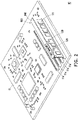
- FIG. 2 is a schematic view of the memory module with the screen of FIG. 1A inserted into a motherboard.
- the motherboard module 10 includes the motherboard 11 and the memory module 100 with the screen.
- the motherboard 11 includes memory slots 11a.
- the connection interface 112 of the memory module 100 with the screen is detachably inserted into the memory slot 11a.
- only four memory slots 11a are schematically illustrated in FIG. 2 . In actuality, the number of the memory slots 11a may also be two or eight, and is not limited thereto.
- the power conversion module 120 and the screen control module 130 receive a signal from the motherboard 11 via the memory slot 11a.
- the power conversion module 120 converts the voltage from the memory slot 11a into the voltage required by the screen 140, and the screen control module 130 processes the signal from the memory slot 11a to control the picture displayed by the screen 140. Therefore, the screen 140 displays text messages or images, such as text messages or images such as the operating frequency or operating temperature of a central processing unit (CPU) to provide users with more functionality.
- CPU central processing unit
- FIG. 3 is a schematic view of a plurality of the memory module with the screen of FIG. 1A inserted into a motherboard.
- a plurality of (for example, four) memory modules 100 with the screen are inserted into the memory slots 11a, the four screens 140 of the four memory modules 100 with the screen are combined into a combined screen S, and the combined screen S displays a large area of text messages or images.
- FIG. 4 is a front view of a memory module with a screen in accordance with an embodiment of the invention.
- FIG. 4 is slightly different from the memory module with the screen of FIG. 1A to FIG. 1B .
- the difference is the height of the memory substrate.
- a memory substrate 110A is the memory substrate 110 heightened.
- Such a memory module 100A with the screen has a greater area, so that the components on the memory substrate 110A may be disposed on the memory substrate 110A with less space limit.
- the memory substrate 110A further includes a standard height region A1 and an expansion region A2.
- the expansion region A2 is disposed beside the standard height region A1 and away from the connection interface 112.
- the sum of the heights of the standard height region A1 and the extension region A2 is greater than 3.048 cm (1.2 inches).
- the memory components 111 are disposed in the standard height region A1, and the power conversion module 120 and the screen control module 130 are disposed on the expansion region A2.
- the configuration of the memory components 111, the power conversion module 120, and the screen control module 130 is not limited thereto, and any configuration in which the components on the memory substrate 110A do not interfere with each other is within the scope of the invention.
- FIG. 5A is a front view of a memory module with a screen in accordance with the present invention.
- FIG. 5B is a perspective view of the memory module with the screen of FIG. 5A .
- a memory module 100B with a screen further includes a heat dissipation cover 160 compared to the memory modules 100 and 100A with the screen.
- the heat dissipation cover 160 is clamped on the memory substrate 110B via a clip B, but is not limited thereto.
- the memory module 100B with the screen may not need the clip B, and instead the heat dissipation cover 160 may be fixed on the memory substrate 110B using a bonding method.
- the heat dissipation cover 160 is disposed on the memory substrate 110B and thermally coupled to the memory components 111. It should be noted that the memory components 111 are covered by the heat dissipation cover 160, so that the memory components cannot be seen in FIG. 5A and FIG. 5B .
- the heat dissipation cover 160 has a surface S, the screen 140 is disposed on the surface S, and the screen 140 is thermally coupled to the surface S. That is to say, the heat dissipation cover 160 has a function of simultaneously helping the memory components 111 and the screen 140 to dissipate heat.
- the surface S is the top surface of the heat dissipation cover 160. In other embodiments not covered by the claims, the surface S may also be the side surface of the heat dissipation cover 160.
- FIG. 6 is a perspective view of a memory module with a screen according to an embodiment not covered by the claims.
- the surface S is a side surface of the heat dissipation cover 160
- the screen 140 is disposed on the surface S of the heat dissipation cover 160.
- the memory modules with the screen in FIGs. 5A and 5B or FIG. 6 may also include the flexible cable 150.
- the flexible cable 150 may also be fixed on the heat dissipation cover 160.
- the fixing method is, for example, engaging, inlaying, or bonding, but is not limited thereto, and any method in which the flexible cable 150 may be fixed to the memory substrate is within the scope of the invention.
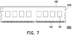
- FIG. 7 is a front view of a memory module with a screen in accordance with the present invention.
- FIG. 8 is a schematic diagram of a motherboard module in accordance with the present invention. Referring to FIG. 7 and FIG. 8 , the main difference between a motherboard module 10C and the motherboard module 10 is that a power conversion module 120C and a screen control module 130C are both disposed on a motherboard 11C.
- the memory module 100C with the screen is inserted into one of the memory slots 11a.
- the power conversion module 120C is disposed on the motherboard 11C and electrically connected to the memory slots 11a.
- the screen control module 130C is disposed on the motherboard 11C and electrically connected to the memory slots 11a and the power conversion module 120C.
- the power conversion module 120C converts the initial voltage from the circuit of the motherboard 11C into the converted voltage required by the screen 140, and the converted voltage passes through one of the empty pins on the connection interface 112 to supply power to the screen 140. That is to say, in the present invention, the voltage passing through the empty pin is the voltage required by the screen 140.
- the advantage of the present invention is that the memory manufacturer does not need to significantly change the design of the memory substrate 110C, and the screen 140 only needs to be disposed on the memory substrate 110C.
- FIG. 8 only schematically shows four memory slots 11a, four power conversion modules 120C and four screen control modules 130C, and in actuality, the number of the memory slots 11a may also be two or eight and is not limited thereto.
- the number of the power conversion module 120C and the screen control modules 130C is configured according to the corresponding number of the memory module 100C with the screen.
- the four screens 140 of the four memory modules 100 with the screen are combined into the combined screen S of FIG. 3 , and the combined screen S displays text messages or images.
- the screen of the memory module with the screen of the invention is electrically connected to the power conversion module and the screen control module, and the power conversion module and the screen control module are electrically connected to the connection interface.
- the power conversion module and the screen control module receive a signal from the motherboard via the memory slot.
- the power conversion module converts the voltage from the memory slot into the voltage required by the screen, and the screen control module processes the signal from the memory slot to control the image displayed by the screen. Therefore, since the screen of the memory module with the screen of the invention shares the memory slots on the motherboard with the memory substrate, the motherboard does not need to have an additional slot for power supply and signal, thereby saving space on the motherboard.
- the screen of the memory module with the screen of the invention displays text messages and images to provide users with more information and visual effects.
- the power conversion module and the screen control module are selectively disposed on the motherboard and electrically connected to the memory slots, so that the screen of the memory module with the screen still obtains the required voltage and control signal via the memory slots.
- the user may operate the screen control module via a software or an application to provide users with a more diverse functionality. In this way, the memory module with the screen may provide more information and entertainment to the user without increasing the burden of motherboard space configuration.
Landscapes
- Engineering & Computer Science (AREA)
- Theoretical Computer Science (AREA)
- General Engineering & Computer Science (AREA)
- Physics & Mathematics (AREA)
- General Physics & Mathematics (AREA)
- Human Computer Interaction (AREA)
- Computer Hardware Design (AREA)
- Power Engineering (AREA)
- Microelectronics & Electronic Packaging (AREA)
- Devices For Indicating Variable Information By Combining Individual Elements (AREA)
- Memory System (AREA)
- Semiconductor Memories (AREA)
- User Interface Of Digital Computer (AREA)
- Multimedia (AREA)
- Control Of Indicators Other Than Cathode Ray Tubes (AREA)
- Debugging And Monitoring (AREA)
Claims (4)
- Ein Motherboard-Modul (10, 10C), das Folgendes aufweist:ein Motherboard (11, 11C), das eine Vielzahl von Speicherschlitzen (11a) aufweist;eine Vielzahl von Speichermodulen (100, 100A, 100B, 100C) mit Bildschirmen, die auf entfernbare Weise in Speicherschlitze (11a) eingesetzt sind, die Folgendes aufweisen:eine Vielzahl von Speichersubstraten (110, 110A, 110B, 110C), wobei jedes der Speichersubstrate (110, 110A, 110B, 110C) eine Vielzahl von Speicherkomponenten (111) und eine Verbindungsschnittstelle (112) aufweist, und die Verbindungschnittstelle (112) auf entfernbare Weise in den entsprechenden Speicherschlitz (11a) eingesetzt ist; undeine Vielzahl von Bildschirmen (140), die auf den Speichersubstraten (110, 110A, 110B, 110C) angeordnet sind;eine Vielzahl von Leistungswandlungsmodulen (120, 120C), die auf den Speichersubstraten (110, 110A, 110B, 110C) angeordnet sind und elektrisch mit der Verbindungsschnittstelle (112) verbunden sind oder auf dem Motherboard (11, 11C) angeordnet sind und elektrisch mit den Speicherschlitzen (11a) verbunden sind; undeine Vielzahl von Bildschirmsteuermodulen (130, 130C), die auf den Speichersubstraten (110, 110A, 110B, 110C) angeordnet sind und elektrisch mit den Verbindungsschnittstellen (112) und den Leistungswandlungsmodulen (120, 120C) verbunden sind oder auf dem Motherboard (11, 11C) angeordnet sind und elektrisch mit den Speicherschlitzen (11a) und den Leistungswandlungsmodulen (120, 120C) verbunden sind,eine Vielzahl von Wärmeabführungsabdeckungen (160), die auf den Speichersubstraten (110, 110A, 110B, 110C) angeordnet sind und thermisch an die Speicherkomponenten (111) gekoppelt sind, wobei jede der Wärmeabführungsabdeckungen (160) eine Oberfläche aufweist, wobei die Oberfläche die Oberseite jeder der Wärmeabführungsabdeckungen (160) ist, die der Verbindungschnittstelle (112) gegenüber liegt, wobei jeder der Vielzahl von Bildschirmen (140) auf der Oberseite jeder der Vielzahl von Wärmeabführungsabdeckungen (160) angeordnet ist, und die Vielzahl von Bildschirmen (140) thermisch an die Wärmeabführungsabdeckungen (160) gekoppelt ist und durch die Wärmeabführungsabdeckungen (160) nicht abgedeckt ist, wobeiwenn die Speichermodule (100, 100A, 100B, 100C) mit den Bildschirmen (140) in die Speicherschlitze (11a) eingesetzt sind, die Vielzahl von Bildschirmen (140) elektrisch mit den Leistungswandlungsmodulen (120, 120C) und den Bildschirmsteuermodulen (130, 130C) verbunden ist zum Empfangen von Spannungen, die durch die Leistungswandlungsmodule (120, 120C) ausgegeben werden und zum Anzeigen von Signalen, die durch die Bildschirmsteuermodule (130, 130C) ausgegeben werden, wobei die Vielzahl von Bildschirmen der Speichermodule mit den Bildschirmen in einen kombinierten Bildschirm zusammengefügt wird, wobei der kombinierte Bildschirm (140) genutzt wird zum Anzeigen von kombinierten Textnachrichten und kombinierten Bildern, wobei jede der Verbindungsschnittstellen (112) serielle Daten und einen seriellen Takt aufweist, und jedes der Bildschirmsteuermodule (130, 130C) elektrisch mit den seriellen Daten und dem seriellen Takt der entsprechenden Verbindungschnittstelle (112) verbunden ist.
- Motherboard-Modul (10, 10C) nach Anspruch 1, wobei die Vielzahl von Leistungswandlungsmodulen (120, 120C) und die Vielzahl von Bildschirmsteuermodulen (130, 130C) elektrisch mit einer Vielzahl von leeren Pins bzw. Kontakten der Verbindungsschnittstellen (112) der Speichersubstrate (110, 110A, 110B, 110C) verbunden sind, wobei die Speichermodule (100, 100A, 100B, 100C) die leeren Pins beim Austauschen von Daten und Leistung mit dem Motherboard (11, 11C) nicht nutzen.
- Motherboard-Modul (10) nach einem der Ansprüche 1-2, wobei, wenn die Vielzahl von Leistungswandlungsmodulen (120, 120C) und die Vielzahl von Bildschirmsteuermodulen (130, 130C) auf den Speichersubstraten angeordnet sind, jedes der Speichersubstrate (110A) mit dem entsprechenden Leistungswandlungsmodul (120) und dem entsprechenden Bildschirmsteuermodul (130) ausgestattet ist, wobei jedes der Speichersubstrate (110A) weiter einen Standardhöhenbereich (A1) und einen Erweiterungsbereich (A2) aufweist, wobei der Erweiterungsbereich (A2) benachbart bzw. angrenzend zu dem Standardhöhenbereich (A1) und weg von der Verbindungsschnittstelle (112) angeordnet ist, und wobei in jedem der Speichersubstrate (110A) die Speicherkomponenten (111) in dem Standardhöhenbereich (A1) angeordnet sind, und das Leistungswandlungsmodul (120) und das Bildschirmsteuermodul (130) auf dem Erweiterungsbereich (A2) angeordnet sind.
- Motherboard-Modul (10, 10C) nach einem der Ansprüche 1-3, wobei die Speichermodule (100, 100A, 100B, 100C) mit den Bildschirmen weiter Folgendes aufweisen:
eine Vielzahl von flexiblen Kabeln (150), die an den Speichersubstraten (110, 110A, 110B, 110C) befestigt sind, wobei die Vielzahl von Bildschirmen (140) mit den Leistungswandlungsmodulen (120, 120C) und den Bildschirmsteuermodulen (130, 130C) über die flexiblen Kabel (150) elektrisch verbunden ist.
Applications Claiming Priority (1)
| Application Number | Priority Date | Filing Date | Title |
|---|---|---|---|
| TW107143174A TWI708182B (zh) | 2018-12-03 | 2018-12-03 | 具有螢幕的記憶體模組與主機板模組 |
Publications (2)
| Publication Number | Publication Date |
|---|---|
| EP3663892A1 EP3663892A1 (de) | 2020-06-10 |
| EP3663892B1 true EP3663892B1 (de) | 2022-08-17 |
Family
ID=68296320
Family Applications (1)
| Application Number | Title | Priority Date | Filing Date |
|---|---|---|---|
| EP19204446.9A Active EP3663892B1 (de) | 2018-12-03 | 2019-10-21 | Speichermodul mit bildschirm und hauptplatinenmodul |
Country Status (6)
| Country | Link |
|---|---|
| US (1) | US11157048B2 (de) |
| EP (1) | EP3663892B1 (de) |
| JP (1) | JP6837528B2 (de) |
| KR (1) | KR20200067737A (de) |
| ES (1) | ES2925643T3 (de) |
| TW (1) | TWI708182B (de) |
Citations (1)
| Publication number | Priority date | Publication date | Assignee | Title |
|---|---|---|---|---|
| US20100315436A1 (en) * | 2009-06-10 | 2010-12-16 | Nexcom International Co. Ltd. | Assembled display device and display frame control method and system |
Family Cites Families (22)
| Publication number | Priority date | Publication date | Assignee | Title |
|---|---|---|---|---|
| JPH0672489B2 (ja) | 1986-11-11 | 1994-09-14 | 戸田建設株式会社 | 自動型枠装置における型枠スパン調節装置 |
| JPH08115399A (ja) | 1994-10-19 | 1996-05-07 | Toshiba Corp | メモリカード |
| JP3533418B2 (ja) | 1999-03-23 | 2004-05-31 | コニカミノルタカメラ株式会社 | デジタルカメラ |
| US7131767B2 (en) * | 2004-08-31 | 2006-11-07 | Pny Technologies, Inc. | Electronic module with built-in temperature display |
| TWI321729B (en) * | 2006-12-13 | 2010-03-11 | Apacer Technology Inc | Dram module with solid state disk |
| CN101894057B (zh) | 2009-05-18 | 2014-01-15 | 鸿富锦精密工业(深圳)有限公司 | 主板故障诊断卡 |
| CN102270164A (zh) | 2010-06-01 | 2011-12-07 | 鸿富锦精密工业(深圳)有限公司 | 电脑主板故障诊断卡 |
| CN202331310U (zh) | 2011-11-07 | 2012-07-11 | 浪潮电子信息产业股份有限公司 | 一种多功能内存安装装置 |
| CN103377106A (zh) * | 2012-04-25 | 2013-10-30 | 鸿富锦精密工业(深圳)有限公司 | 侦测识别电路 |
| CN103793303A (zh) | 2012-11-01 | 2014-05-14 | 谢强 | 一种基于计算机主板的内存条测试卡 |
| TWI492049B (zh) * | 2013-02-06 | 2015-07-11 | Ibm | 記憶體模組狀態指示方法及裝置 |
| TWI522784B (zh) * | 2015-01-20 | 2016-02-21 | 宇帷國際股份有限公司 | 電子裝置 |
| TWI519050B (zh) * | 2015-01-20 | 2016-01-21 | 宇帷國際股份有限公司 | 電子裝置及其電路模組 |
| TWM508053U (zh) * | 2015-05-12 | 2015-09-01 | Avexir Technologies Corp | 電路模組 |
| US10429568B2 (en) * | 2015-10-30 | 2019-10-01 | Alson Technology Limited | Dynamic random access memory |
| US9839121B2 (en) * | 2015-11-13 | 2017-12-05 | Alson Technology Limited | Electronic device and dynamic random access memory thereof |
| CN205230594U (zh) * | 2015-12-01 | 2016-05-11 | 宇帷国际股份有限公司 | 动态随机存取记忆体 |
| US10001963B2 (en) * | 2015-12-01 | 2018-06-19 | Alson Technology Limited | Dynamic random access memory |
| US9723697B1 (en) * | 2016-01-27 | 2017-08-01 | Alson Technology Limited | System for alternating light-emitting of dynamic random access memory |
| US20170339465A1 (en) | 2016-05-18 | 2017-11-23 | copper studios, inc. | Viewing habit influenced clip and sequence selection in an individualized video delivery system |
| TWI592057B (zh) * | 2016-05-30 | 2017-07-11 | 宇瞻科技股份有限公司 | 發光裝置及其控制方法 |
| TWI599872B (zh) * | 2016-07-22 | 2017-09-21 | 宇瞻科技股份有限公司 | 具均勻出光之擴充卡及其均光裝置 |
-
2018
- 2018-12-03 TW TW107143174A patent/TWI708182B/zh active
-
2019
- 2019-09-03 US US16/558,343 patent/US11157048B2/en active Active
- 2019-10-01 KR KR1020190121550A patent/KR20200067737A/ko not_active Ceased
- 2019-10-07 JP JP2019184730A patent/JP6837528B2/ja active Active
- 2019-10-21 EP EP19204446.9A patent/EP3663892B1/de active Active
- 2019-10-21 ES ES19204446T patent/ES2925643T3/es active Active
Patent Citations (1)
| Publication number | Priority date | Publication date | Assignee | Title |
|---|---|---|---|---|
| US20100315436A1 (en) * | 2009-06-10 | 2010-12-16 | Nexcom International Co. Ltd. | Assembled display device and display frame control method and system |
Also Published As
| Publication number | Publication date |
|---|---|
| JP2020091845A (ja) | 2020-06-11 |
| US11157048B2 (en) | 2021-10-26 |
| JP6837528B2 (ja) | 2021-03-03 |
| ES2925643T3 (es) | 2022-10-19 |
| US20200174532A1 (en) | 2020-06-04 |
| EP3663892A1 (de) | 2020-06-10 |
| KR20200067737A (ko) | 2020-06-12 |
| TW202022593A (zh) | 2020-06-16 |
| TWI708182B (zh) | 2020-10-21 |
Similar Documents
| Publication | Publication Date | Title |
|---|---|---|
| KR102747080B1 (ko) | 플렉서블 디스플레이 모듈 및 이를 포함하는 전자 기기 | |
| US6629181B1 (en) | Incremental bus structure for modular electronic equipment | |
| KR102517092B1 (ko) | 가요성 디스플레이 패널을 포함하는 전자 장치 | |
| KR20170098373A (ko) | 터치 스크린 패널 및 이를 포함하는 이동 단말기 | |
| US6216184B1 (en) | Extended riser for implementing a cableless front panel input/output | |
| AU2018265974A1 (en) | Splicing screen, display device and mobile terminal | |
| CN205068333U (zh) | 电子显示模块及电子装置 | |
| US7354275B2 (en) | Graphics card connector module, and motherboard device having the same | |
| CN112639663B (zh) | 显示装置及电子设备 | |
| WO2020149588A1 (ko) | 슬릿을 구비한 인쇄회로기판을 포함하는 전자 장치 | |
| US11947879B2 (en) | Interactive information system with modular structure | |
| US11157048B2 (en) | Memory module with screen and motherboard module | |
| CN111258385B (zh) | 具有屏幕的记忆体模块与主机板模块 | |
| CN108008764A (zh) | 电路板组合 | |
| KR100499585B1 (ko) | 통합형 메인보드 | |
| US6947036B2 (en) | Liquid crystal display with space-saving conversion module | |
| CN213303612U (zh) | 显示屏结构、液晶显示屏以及显示装置 | |
| KR200239759Y1 (ko) | 통합형 메인보드 | |
| US20040145685A1 (en) | Conversion module for liquid crystal display | |
| KR100800686B1 (ko) | 엘시디 모듈과 그를 이용한 액정 영상 수단 | |
| CN116520575A (zh) | 一种头戴式数字像源及配置方法 | |
| JP3191027U (ja) | 情報処理装置 | |
| KR101247030B1 (ko) | 그래픽 컨트롤러 브리지 모듈 및 이를 구비하는 휴대용컴퓨터 | |
| WO2023027482A1 (ko) | 디스플레이 모듈 및 이를 포함하는 전자 장치 | |
| US20060291180A1 (en) | PCI mezzanine card |
Legal Events
| Date | Code | Title | Description |
|---|---|---|---|
| PUAI | Public reference made under article 153(3) epc to a published international application that has entered the european phase |
Free format text: ORIGINAL CODE: 0009012 |
|
| STAA | Information on the status of an ep patent application or granted ep patent |
Free format text: STATUS: THE APPLICATION HAS BEEN PUBLISHED |
|
| AK | Designated contracting states |
Kind code of ref document: A1 Designated state(s): AL AT BE BG CH CY CZ DE DK EE ES FI FR GB GR HR HU IE IS IT LI LT LU LV MC MK MT NL NO PL PT RO RS SE SI SK SM TR |
|
| AX | Request for extension of the european patent |
Extension state: BA ME |
|
| STAA | Information on the status of an ep patent application or granted ep patent |
Free format text: STATUS: REQUEST FOR EXAMINATION WAS MADE |
|
| 17P | Request for examination filed |
Effective date: 20200910 |
|
| RBV | Designated contracting states (corrected) |
Designated state(s): AL AT BE BG CH CY CZ DE DK EE ES FI FR GB GR HR HU IE IS IT LI LT LU LV MC MK MT NL NO PL PT RO RS SE SI SK SM TR |
|
| STAA | Information on the status of an ep patent application or granted ep patent |
Free format text: STATUS: EXAMINATION IS IN PROGRESS |
|
| 17Q | First examination report despatched |
Effective date: 20201215 |
|
| GRAP | Despatch of communication of intention to grant a patent |
Free format text: ORIGINAL CODE: EPIDOSNIGR1 |
|
| STAA | Information on the status of an ep patent application or granted ep patent |
Free format text: STATUS: GRANT OF PATENT IS INTENDED |
|
| INTG | Intention to grant announced |
Effective date: 20220315 |
|
| GRAS | Grant fee paid |
Free format text: ORIGINAL CODE: EPIDOSNIGR3 |
|
| GRAA | (expected) grant |
Free format text: ORIGINAL CODE: 0009210 |
|
| STAA | Information on the status of an ep patent application or granted ep patent |
Free format text: STATUS: THE PATENT HAS BEEN GRANTED |
|
| AK | Designated contracting states |
Kind code of ref document: B1 Designated state(s): AL AT BE BG CH CY CZ DE DK EE ES FI FR GB GR HR HU IE IS IT LI LT LU LV MC MK MT NL NO PL PT RO RS SE SI SK SM TR |
|
| REG | Reference to a national code |
Ref country code: CH Ref legal event code: EP |
|
| REG | Reference to a national code |
Ref country code: DE Ref legal event code: R096 Ref document number: 602019018320 Country of ref document: DE |
|
| REG | Reference to a national code |
Ref country code: IE Ref legal event code: FG4D |
|
| REG | Reference to a national code |
Ref country code: AT Ref legal event code: REF Ref document number: 1512593 Country of ref document: AT Kind code of ref document: T Effective date: 20220915 |
|
| REG | Reference to a national code |
Ref country code: ES Ref legal event code: FG2A Ref document number: 2925643 Country of ref document: ES Kind code of ref document: T3 Effective date: 20221019 |
|
| REG | Reference to a national code |
Ref country code: NL Ref legal event code: MP Effective date: 20220817 |
|
| REG | Reference to a national code |
Ref country code: LT Ref legal event code: MG9D |
|
| PG25 | Lapsed in a contracting state [announced via postgrant information from national office to epo] |
Ref country code: SE Free format text: LAPSE BECAUSE OF FAILURE TO SUBMIT A TRANSLATION OF THE DESCRIPTION OR TO PAY THE FEE WITHIN THE PRESCRIBED TIME-LIMIT Effective date: 20220817 Ref country code: RS Free format text: LAPSE BECAUSE OF FAILURE TO SUBMIT A TRANSLATION OF THE DESCRIPTION OR TO PAY THE FEE WITHIN THE PRESCRIBED TIME-LIMIT Effective date: 20220817 Ref country code: PT Free format text: LAPSE BECAUSE OF FAILURE TO SUBMIT A TRANSLATION OF THE DESCRIPTION OR TO PAY THE FEE WITHIN THE PRESCRIBED TIME-LIMIT Effective date: 20221219 Ref country code: NO Free format text: LAPSE BECAUSE OF FAILURE TO SUBMIT A TRANSLATION OF THE DESCRIPTION OR TO PAY THE FEE WITHIN THE PRESCRIBED TIME-LIMIT Effective date: 20221117 Ref country code: NL Free format text: LAPSE BECAUSE OF FAILURE TO SUBMIT A TRANSLATION OF THE DESCRIPTION OR TO PAY THE FEE WITHIN THE PRESCRIBED TIME-LIMIT Effective date: 20220817 Ref country code: LV Free format text: LAPSE BECAUSE OF FAILURE TO SUBMIT A TRANSLATION OF THE DESCRIPTION OR TO PAY THE FEE WITHIN THE PRESCRIBED TIME-LIMIT Effective date: 20220817 Ref country code: LT Free format text: LAPSE BECAUSE OF FAILURE TO SUBMIT A TRANSLATION OF THE DESCRIPTION OR TO PAY THE FEE WITHIN THE PRESCRIBED TIME-LIMIT Effective date: 20220817 Ref country code: FI Free format text: LAPSE BECAUSE OF FAILURE TO SUBMIT A TRANSLATION OF THE DESCRIPTION OR TO PAY THE FEE WITHIN THE PRESCRIBED TIME-LIMIT Effective date: 20220817 |
|
| REG | Reference to a national code |
Ref country code: AT Ref legal event code: MK05 Ref document number: 1512593 Country of ref document: AT Kind code of ref document: T Effective date: 20220817 |
|
| PG25 | Lapsed in a contracting state [announced via postgrant information from national office to epo] |
Ref country code: PL Free format text: LAPSE BECAUSE OF FAILURE TO SUBMIT A TRANSLATION OF THE DESCRIPTION OR TO PAY THE FEE WITHIN THE PRESCRIBED TIME-LIMIT Effective date: 20220817 Ref country code: IS Free format text: LAPSE BECAUSE OF FAILURE TO SUBMIT A TRANSLATION OF THE DESCRIPTION OR TO PAY THE FEE WITHIN THE PRESCRIBED TIME-LIMIT Effective date: 20221217 Ref country code: HR Free format text: LAPSE BECAUSE OF FAILURE TO SUBMIT A TRANSLATION OF THE DESCRIPTION OR TO PAY THE FEE WITHIN THE PRESCRIBED TIME-LIMIT Effective date: 20220817 Ref country code: GR Free format text: LAPSE BECAUSE OF FAILURE TO SUBMIT A TRANSLATION OF THE DESCRIPTION OR TO PAY THE FEE WITHIN THE PRESCRIBED TIME-LIMIT Effective date: 20221118 |
|
| PG25 | Lapsed in a contracting state [announced via postgrant information from national office to epo] |
Ref country code: SM Free format text: LAPSE BECAUSE OF FAILURE TO SUBMIT A TRANSLATION OF THE DESCRIPTION OR TO PAY THE FEE WITHIN THE PRESCRIBED TIME-LIMIT Effective date: 20220817 Ref country code: RO Free format text: LAPSE BECAUSE OF FAILURE TO SUBMIT A TRANSLATION OF THE DESCRIPTION OR TO PAY THE FEE WITHIN THE PRESCRIBED TIME-LIMIT Effective date: 20220817 Ref country code: DK Free format text: LAPSE BECAUSE OF FAILURE TO SUBMIT A TRANSLATION OF THE DESCRIPTION OR TO PAY THE FEE WITHIN THE PRESCRIBED TIME-LIMIT Effective date: 20220817 Ref country code: CZ Free format text: LAPSE BECAUSE OF FAILURE TO SUBMIT A TRANSLATION OF THE DESCRIPTION OR TO PAY THE FEE WITHIN THE PRESCRIBED TIME-LIMIT Effective date: 20220817 Ref country code: AT Free format text: LAPSE BECAUSE OF FAILURE TO SUBMIT A TRANSLATION OF THE DESCRIPTION OR TO PAY THE FEE WITHIN THE PRESCRIBED TIME-LIMIT Effective date: 20220817 |
|
| REG | Reference to a national code |
Ref country code: DE Ref legal event code: R097 Ref document number: 602019018320 Country of ref document: DE |
|
| PG25 | Lapsed in a contracting state [announced via postgrant information from national office to epo] |
Ref country code: SK Free format text: LAPSE BECAUSE OF FAILURE TO SUBMIT A TRANSLATION OF THE DESCRIPTION OR TO PAY THE FEE WITHIN THE PRESCRIBED TIME-LIMIT Effective date: 20220817 Ref country code: MC Free format text: LAPSE BECAUSE OF FAILURE TO SUBMIT A TRANSLATION OF THE DESCRIPTION OR TO PAY THE FEE WITHIN THE PRESCRIBED TIME-LIMIT Effective date: 20220817 Ref country code: EE Free format text: LAPSE BECAUSE OF FAILURE TO SUBMIT A TRANSLATION OF THE DESCRIPTION OR TO PAY THE FEE WITHIN THE PRESCRIBED TIME-LIMIT Effective date: 20220817 |
|
| REG | Reference to a national code |
Ref country code: CH Ref legal event code: PL |
|
| PLBE | No opposition filed within time limit |
Free format text: ORIGINAL CODE: 0009261 |
|
| STAA | Information on the status of an ep patent application or granted ep patent |
Free format text: STATUS: NO OPPOSITION FILED WITHIN TIME LIMIT |
|
| REG | Reference to a national code |
Ref country code: BE Ref legal event code: MM Effective date: 20221031 |
|
| PG25 | Lapsed in a contracting state [announced via postgrant information from national office to epo] |
Ref country code: LU Free format text: LAPSE BECAUSE OF NON-PAYMENT OF DUE FEES Effective date: 20221021 Ref country code: AL Free format text: LAPSE BECAUSE OF FAILURE TO SUBMIT A TRANSLATION OF THE DESCRIPTION OR TO PAY THE FEE WITHIN THE PRESCRIBED TIME-LIMIT Effective date: 20220817 |
|
| 26N | No opposition filed |
Effective date: 20230519 |
|
| PG25 | Lapsed in a contracting state [announced via postgrant information from national office to epo] |
Ref country code: LI Free format text: LAPSE BECAUSE OF NON-PAYMENT OF DUE FEES Effective date: 20221031 Ref country code: CH Free format text: LAPSE BECAUSE OF NON-PAYMENT OF DUE FEES Effective date: 20221031 |
|
| PG25 | Lapsed in a contracting state [announced via postgrant information from national office to epo] |
Ref country code: SI Free format text: LAPSE BECAUSE OF FAILURE TO SUBMIT A TRANSLATION OF THE DESCRIPTION OR TO PAY THE FEE WITHIN THE PRESCRIBED TIME-LIMIT Effective date: 20220817 |
|
| PG25 | Lapsed in a contracting state [announced via postgrant information from national office to epo] |
Ref country code: BE Free format text: LAPSE BECAUSE OF NON-PAYMENT OF DUE FEES Effective date: 20221031 |
|
| PG25 | Lapsed in a contracting state [announced via postgrant information from national office to epo] |
Ref country code: IE Free format text: LAPSE BECAUSE OF NON-PAYMENT OF DUE FEES Effective date: 20221021 |
|
| PG25 | Lapsed in a contracting state [announced via postgrant information from national office to epo] |
Ref country code: HU Free format text: LAPSE BECAUSE OF FAILURE TO SUBMIT A TRANSLATION OF THE DESCRIPTION OR TO PAY THE FEE WITHIN THE PRESCRIBED TIME-LIMIT; INVALID AB INITIO Effective date: 20191021 |
|
| PG25 | Lapsed in a contracting state [announced via postgrant information from national office to epo] |
Ref country code: CY Free format text: LAPSE BECAUSE OF FAILURE TO SUBMIT A TRANSLATION OF THE DESCRIPTION OR TO PAY THE FEE WITHIN THE PRESCRIBED TIME-LIMIT Effective date: 20220817 |
|
| PG25 | Lapsed in a contracting state [announced via postgrant information from national office to epo] |
Ref country code: MK Free format text: LAPSE BECAUSE OF FAILURE TO SUBMIT A TRANSLATION OF THE DESCRIPTION OR TO PAY THE FEE WITHIN THE PRESCRIBED TIME-LIMIT Effective date: 20220817 Ref country code: IT Free format text: LAPSE BECAUSE OF FAILURE TO SUBMIT A TRANSLATION OF THE DESCRIPTION OR TO PAY THE FEE WITHIN THE PRESCRIBED TIME-LIMIT Effective date: 20220817 |
|
| PG25 | Lapsed in a contracting state [announced via postgrant information from national office to epo] |
Ref country code: TR Free format text: LAPSE BECAUSE OF FAILURE TO SUBMIT A TRANSLATION OF THE DESCRIPTION OR TO PAY THE FEE WITHIN THE PRESCRIBED TIME-LIMIT Effective date: 20220817 |
|
| PG25 | Lapsed in a contracting state [announced via postgrant information from national office to epo] |
Ref country code: BG Free format text: LAPSE BECAUSE OF FAILURE TO SUBMIT A TRANSLATION OF THE DESCRIPTION OR TO PAY THE FEE WITHIN THE PRESCRIBED TIME-LIMIT Effective date: 20220817 |
|
| PG25 | Lapsed in a contracting state [announced via postgrant information from national office to epo] |
Ref country code: MT Free format text: LAPSE BECAUSE OF FAILURE TO SUBMIT A TRANSLATION OF THE DESCRIPTION OR TO PAY THE FEE WITHIN THE PRESCRIBED TIME-LIMIT Effective date: 20220817 |
|
| PGFP | Annual fee paid to national office [announced via postgrant information from national office to epo] |
Ref country code: GB Payment date: 20250904 Year of fee payment: 7 |
|
| PGFP | Annual fee paid to national office [announced via postgrant information from national office to epo] |
Ref country code: FR Payment date: 20250908 Year of fee payment: 7 |
|
| PGFP | Annual fee paid to national office [announced via postgrant information from national office to epo] |
Ref country code: DE Payment date: 20250902 Year of fee payment: 7 |
|
| PGFP | Annual fee paid to national office [announced via postgrant information from national office to epo] |
Ref country code: ES Payment date: 20251107 Year of fee payment: 7 |