EP3647839B1 - Stepped structure optical filter - Google Patents
Stepped structure optical filter Download PDFInfo
- Publication number
- EP3647839B1 EP3647839B1 EP19206709.8A EP19206709A EP3647839B1 EP 3647839 B1 EP3647839 B1 EP 3647839B1 EP 19206709 A EP19206709 A EP 19206709A EP 3647839 B1 EP3647839 B1 EP 3647839B1
- Authority
- EP
- European Patent Office
- Prior art keywords
- spacer
- mirror
- filter
- medium
- stepped
- Prior art date
- Legal status (The legal status is an assumption and is not a legal conclusion. Google has not performed a legal analysis and makes no representation as to the accuracy of the status listed.)
- Active
Links
Images


Classifications
-
- G—PHYSICS
- G02—OPTICS
- G02B—OPTICAL ELEMENTS, SYSTEMS OR APPARATUS
- G02B5/00—Optical elements other than lenses
- G02B5/20—Filters
- G02B5/201—Filters in the form of arrays
-
- G—PHYSICS
- G02—OPTICS
- G02B—OPTICAL ELEMENTS, SYSTEMS OR APPARATUS
- G02B26/00—Optical devices or arrangements for the control of light using movable or deformable optical elements
- G02B26/001—Optical devices or arrangements for the control of light using movable or deformable optical elements based on interference in an adjustable optical cavity
-
- G—PHYSICS
- G02—OPTICS
- G02B—OPTICAL ELEMENTS, SYSTEMS OR APPARATUS
- G02B5/00—Optical elements other than lenses
- G02B5/08—Mirrors
- G02B5/0816—Multilayer mirrors, i.e. having two or more reflecting layers
-
- G—PHYSICS
- G02—OPTICS
- G02B—OPTICAL ELEMENTS, SYSTEMS OR APPARATUS
- G02B5/00—Optical elements other than lenses
- G02B5/20—Filters
- G02B5/26—Reflecting filters
-
- G—PHYSICS
- G02—OPTICS
- G02B—OPTICAL ELEMENTS, SYSTEMS OR APPARATUS
- G02B5/00—Optical elements other than lenses
- G02B5/20—Filters
- G02B5/28—Interference filters
- G02B5/285—Interference filters comprising deposited thin solid films
- G02B5/288—Interference filters comprising deposited thin solid films comprising at least one thin film resonant cavity, e.g. in bandpass filters
-
- H—ELECTRICITY
- H10—SEMICONDUCTOR DEVICES; ELECTRIC SOLID-STATE DEVICES NOT OTHERWISE PROVIDED FOR
- H10F—INORGANIC SEMICONDUCTOR DEVICES SENSITIVE TO INFRARED RADIATION, LIGHT, ELECTROMAGNETIC RADIATION OF SHORTER WAVELENGTH OR CORPUSCULAR RADIATION
- H10F39/00—Integrated devices, or assemblies of multiple devices, comprising at least one element covered by group H10F30/00, e.g. radiation detectors comprising photodiode arrays
- H10F39/011—Manufacture or treatment of image sensors covered by group H10F39/12
- H10F39/024—Manufacture or treatment of image sensors covered by group H10F39/12 of coatings or optical elements
-
- H—ELECTRICITY
- H10—SEMICONDUCTOR DEVICES; ELECTRIC SOLID-STATE DEVICES NOT OTHERWISE PROVIDED FOR
- H10F—INORGANIC SEMICONDUCTOR DEVICES SENSITIVE TO INFRARED RADIATION, LIGHT, ELECTROMAGNETIC RADIATION OF SHORTER WAVELENGTH OR CORPUSCULAR RADIATION
- H10F39/00—Integrated devices, or assemblies of multiple devices, comprising at least one element covered by group H10F30/00, e.g. radiation detectors comprising photodiode arrays
- H10F39/80—Constructional details of image sensors
- H10F39/806—Optical elements or arrangements associated with the image sensors
- H10F39/8067—Reflectors
Definitions
- the present invention relates to a stepped optical filter and an system comprising the same.
- An optical transmitter may emit light that is directed toward an object.
- the optical transmitter may transmit near infrared light toward a user, and the near-infrared light may be reflected off the user toward an optical receiver.
- the optical receiver may capture information regarding the near-infrared light, and the information may be used to identify a gesture being performed by the user.
- information regarding the visible light such as information regarding different wavelengths of visible light may be captured to image an object.
- ambient light may be introduced along with the wavelength of interest.
- the optical receiver may also receive visible light (e.g., from another light source, such as a light bulb or the sun).
- the optical receiver may be optically coupled to an optical filter, such as a bandpass filter, to filter ambient light and to allow one or more wavelengths of light to pass through toward the optical receiver.
- an optical filter such as a bandpass filter
- a filter may be provided to ensure that each wavelength of light, of the multiple wavelengths of light, is directed to a different sensor.
- a multispectral sensor device which may be an optical receiver, may be utilized to capture information about the multiple wavelengths of light.
- the multispectral sensor device may include a set of sensor elements (e.g., optical sensors, spectral sensors, and/or image sensors) that capture the information and are coupled to a multispectral filter.
- sensor elements e.g., optical sensors, spectral sensors, and/or image sensors
- an array of sensor elements may be utilized to capture information relating to multiple frequencies, and the multispectral filter may direct, to each sensor element, light associated with a different frequency.
- a single binary multispectral filter may be disposed to cover each sensor element of the sensor element array, and may form a set of channels for the sensor element array.
- a filter as set out in claim 1.
- the stepped medium may be stepped in one dimension.
- the stepped medium may be stepped in two dimensions.
- a wavelength range of the set of channels of the filter may be between approximately 380 nanometers (nm) and 780 nm.
- a wavelength range of the set of channels of the filter may be between approximately 750 nanometers (nm) and 1100 nm.
- the stepped medium may be associated with a greater than 70% transmissivity at a wavelength range of the filter and is one of: an oxide based medium, a semiconductor based medium, a dielectric based medium, a polymer based medium, a nitride based medium, a phosphide based medium, or a carbide based medium.
- the spacer may be associated with a refractive index greater than 1.7 and is one of: hydrogenated silicon based spacer, an oxide based spacer, a germanium based spacer, or a silicon germanium based spacer.
- the spacer may be at least one of: a gaseous spacer, a polymer spacer, or a liquid spacer.
- the stepped medium forms a set of pillars, and wherein at least one pillar, of the set of pillars, forms an inactive channel.
- a sensor element may be incorporated into an optical sensor device to obtain information (e.g., spectral data) regarding a set of electromagnetic frequencies.
- the optical sensor device may include an image sensor, a multispectral sensor, and/or the like that may perform a sensor measurement of light.
- the optical sensor device may utilize one or more sensor technologies, such as a complementary metal-oxide-semiconductor (CMOS) technology, a charge-coupled device (CCD) technology, and/or the like.
- CMOS complementary metal-oxide-semiconductor
- CCD charge-coupled device
- the optical sensor device may include multiple sensor elements (e.g., an array of sensor elements) each configured to obtain information about a different frequency of light.
- a sensor element may be associated with a filter that filters light to the sensor element.
- the sensor element may be aligned with a linear variable filter (LVF), a circular variable filter (CVF), a Fabry-Perot filter, and/or the like to cause a portion of light directed toward the sensor element to be filtered.
- a binary filter structure such as a Fabry-Perot filter
- a spacer may be positioned between reflectors (e.g., mirrors) of the binary filter structure. Configuration of refractive indices, thicknesses, and/or the like of layers of the reflectors, layers of the spacer, and/or the like may enable configuration of the binary filter structure to form a set of channels.
- a channel may be a portion of the filter that directs light of a particular wavelength range to a sensor element of a sensor element array. In this way, the sensor element array may obtain information regarding multiple different wavelengths of light.
- a fixed set of channels configured based at least in part on selected refractive indices, spacer thicknesses, and/or the like may limit a sensor element array to performing measurements of a fixed set of wavelengths.
- the binary multispectral filter may be designed with greater than a threshold quantity of channels and a sensor element array may, correspondingly, include greater than a threshold quantity of sensor elements. This may result in excessive size and/or an excessive cost to ensure flexibility in using a binary multispectral filter.
- some binary multispectral filters use different spacer thicknesses to form different channels at different wavelength ranges.
- the different spacer thicknesses may be formed by depositing multiple layers of a spacer material on top of a first flat mirror, which is deposited directly on a substrate.
- the multiple layers of the spacer material are deposited to form a stepped structure spacer, and a second mirror is deposited onto the stepped structure of the spacer.
- depositing multiple layers of the spacer material may result in imperfections, which may reduce optical performance of a binary multispectral filter.
- a surface of each layer of the hydrogenated silicon may partially oxidize into silicon dioxide in between layer depositions, which may result in a reduced transmissivity, an increased angle shift, and/or the like.
- a binary multispectral filter may include a stepped medium disposed between a substrate and a first mirror, causing the first mirror to have a stepped surface, a monolithic spacer disposed on the stepped surface of the mirror, and a second mirror disposed on a flat surface of the monolithic spacer.
- imperfections such as surface oxidation, may be avoided, thereby improving optical performance.
- a monolithic spacer may enable improved transmissivity, reduced angle shift, and/or the like.
- some implementations may enable the second mirror to be movable with respect to the first mirror, rather than disposed directly on the spacer and disposed in a fixed position.
- the second mirror may be translatable relative to the first mirror (i.e., either the first mirror or the second mirror or both the first mirror and the second mirror may be moved), thereby enabling a gap between the first mirror and the second mirror, formed by the spacer, to vary in thickness as the second mirror is translated.
- a wavelength range of a set of channels may be dynamically reconfigurable, thereby increasing a quantity of spectral bands that can be captured by sensor elements aligned to the set of channels.
- a quantity of channels in the multispectral filter to cover a particular spectral range may be decreased relative to a multispectral filter with a fixed gap between mirrors, thereby achieving reduced size, reduced cost, and/or the like.
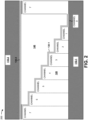
- Fig. 1 is a diagram of an example implementation of a multispectral filter 100 described herein.
- a multispectral filter 100 e.g., a binary structure optical filter array
- a substrate 110 includes a substrate 110, a medium 120, a first mirror 130-1, a second mirror 130-2, and a spacer 140.
- substrate 110 may be associated with an optical sensor device.
- substrate 110 may include an array of sensor elements to capture information (e.g., spectral data).
- substrate 110 may not include sensor elements, and multispectral filter 100 may be aligned to sensor elements disposed on another substrate.
- multispectral filter 100 may be designed without substrate 110.
- multispectral filter 100 may be positioned in free space, may be disposed onto a substrate of an optical sensor device not part of multispectral filter 100, and/or the like.
- multispectral filter 100 may be associated with a particular spectral range.
- multispectral filter 100 may be associated with multiple channels in a visible spectral range, a near infrared (NIR) spectral range, a mid-infrared (MIR) spectral range, and/or the like.
- NIR near infrared
- MIR mid-infrared
- multispectral filter 100 may be associated with a spectral range of between approximately 300 nanometers (nm) and 2500 nm, 360 nanometers (nm) and 2500 nm, between approximately 600 nm and approximately 2000 nm, between approximately 350 nm and approximately 750 nm, 380 nm and approximately 780 nm, between approximately 750 nm and approximately 1500 nm, 750 nm and approximately 1100 nm, 900 nm and approximately 2500 nm, between approximately 900 nm and approximately 1700 nm, between approximately 900 nm and approximately 1500 nm, and/or the like.
- multispectral filter 100 may include a threshold quantity of channels, such as greater than or equal to 8 channels, 16 channels, 32 channels, 64 channels, 128 channels, 256 channels, and/or the like.
- medium 120 is associated with a stepped structure, which forms a set of channels for multispectral filter 100.
- medium 120 may be formed, as described in more detail herein, using a photolithographic procedure to form the stepped structure.
- medium 120 may be stepped along a single axis (i.e., stepped in one dimension), as shown.
- medium 120 may be stepped to form a set of 8 different channels extending along the single axis.
- medium 120 may be stepped along multiple axes (i.e., stepped in two dimensions).
- medium 120 may be stepped orthogonal to the single axis to form a total of 64 different channels.
- medium 120 may include one or more repeated channels.
- Channel 7 formed by medium 120 may be disposed at edges of multispectral filter 100, which provides structural stability for multispectral filter 100.
- Medium 120 causes one or more channels to be inactive.
- portions of first mirror 130-1 and second mirror 130-2, which are aligned with a pillar of medium 120 forming Channel 7, do not sandwich a portion of spacer 140. This results in Channel 7 being inactive (but remaining for structural support).
- a portion of spacer 140 may be sandwiched by first mirror 130-1 and second mirror 130-2 to cause Channel 7 to be an active channel.
- medium 120 may be formed using a particular material.
- medium 120 may be formed from a material that is transmissive to a wavelength range for which multispectral filter 100 is to capture spectral data.
- the material may include a tantalum based medium material, a niobium based medium material, a silicon dioxide based medium material, an oxide based medium material, a III-V semiconductor based medium material, a gallium phosphide based medium material, a germanium based medium material, germanium silicon based medium material, a dielectric based medium material, a polymer based medium material, a nitride based medium material, a phosphide based medium material, a carbide based medium material, a combination thereof, and/or the like.
- first mirror 130-1 and second mirror 130-2 may sandwich spacer 140.
- spacer 140 may separate first mirror 130-1 and second mirror 130-2 by a set of distances and/or faces of spacer 140 may be enclosed by first mirror 130-1 and second mirror 130-2.
- the set of distances may form different channels.
- a first portion of first mirror 130-1 and second mirror 130-2 aligned to Channel 0 may be separated by a first distance, and may form a first channel that passes through a first wavelength band of light.
- first mirror 130-1 and second mirror 130-2 aligned to Channel 1 may be separated by a second distance, as a result of medium 120 having a stepped structure and causing a stepped structure for spacer 140, as described in more detail herein, and may form a second channel that passes through a second wavelength band of light.
- the first channel may be aligned to a first sensor element and may form a first component filter for obtaining spectral data regarding the first spectral range
- the second channel may be aligned to a second sensor element and may form a second component filter for obtaining spectral data regarding the second spectral range.
- mirrors 130 may be associated with a particular material.
- mirrors 130 may include a set of metal mirror layers (e.g., silver), a set of dielectric mirror layers (e.g., alternating hydrogenated silicon layers and silicon dioxide layers), and/or the like to direct a portion of light directed from a light source toward sensor elements associated with multispectral filter 100.
- mirrors 130 may align with each sensor element, of a sensor element array, associated with each channel of multispectral filter 100.
- spacer 140 may be a monolithically formed spacer, as described in more detail herein.
- spacer 140 may be formed by depositing a material onto a stepped surface of first mirror 130-1, such that a first surface of spacer 140 at an interface with first mirror 130-1 is a stepped surface and a second surface of spacer 140 at an interface with second mirror 130-2 is a flat surface.
- spacer 140 may be formed from a particular material to cause multispectral filter 100 to have a particular wavelength range, transmissivity (e.g., greater than 50%, greater than 70%, greater than 90%, greater than 95%, greater than 99%, greater than 99.9%, greater than 99.99%, etc.), and/or the like.
- spacer 140 may be a hydrogenated silicon based spacer, an oxide based spacer, a germanium based spacer, a silicon germanium based spacer, a polymer spacer, a combination thereof, and/or the like.
- spacer 140 may have a refractive index greater than 1.5, greater than 1.7, greater than 2.5, greater than 3.0, greater than 3.5, and/or the like.
- spacer 140 may include a non-solid spacer material.
- spacer 140 may be formed from a gaseous material (e.g., air or another gaseous material) or a liquid material to enable a size of spacer 140 (i.e., a separation between first mirror 130-1 and second mirror 130-2) to be expanded or contracted, as described in more detail herein.
- spacer 140 may include multiple spacer materials.
- spacer 140 may include a solid spacer forming a first portion of spacer 140 and covering first mirror 130-1 and a liquid spacer forming a second portion of spacer 140 and enabling second mirror 130-2 to be translated with respect to first mirror 130-1.
- spacer 140 may include a first solid spacer covering first mirror 130-1, a second solid spacer covering second mirror 130-2, and a third liquid spacer disposed between the first solid spacer and the second solid spacer to enable second mirror 130-2 to be translated with respect to first mirror 130-1.
- spacer 140 enables different portions of multispectral filter 100 to pass different wavelength bands of light to form different channels.
- spacer 140 may be associated with less than a threshold level of imperfections, such as less than a threshold amount of surface oxidation within spacer 140, thereby improving optical performance of multispectral filter 100.
- layers forming, for example, medium 120, first mirror 130-1, second mirror 130-2, spacer 140, and/or the like may include a set of layers of a high refractive index material (H layers), such as silicon layers, hydrogenated silicon layers, silicon-germanium (SiGe) layers, hydrogenated germanium layers, hydrogenated silicon-germanium layers, and/or the like.
- H layers high refractive index material
- the layers forming, for example, medium 120, first mirror 130-1, second mirror 130-2, spacer 140, and/or the like may include a set of a low refractive index material (L layers), such as silicon dioxide layers, silicon nitride layers, tantalum pentoxide (Ta 2 O 5 ) layers, niobium pentoxide (Nb 2 O 5 ) layers, titanium dioxide (TiO 2 ) layers, aluminum oxide (Al 2 O 3 ) layers, zirconium oxide (ZrO 2 ) layers, yttrium oxide (Y 2 O 3 ) layers, silicon nitride (Si 3 N 4 ) layers, a combination thereof, and/or the like.
- L layers low refractive index material
- L layers such as silicon dioxide layers, silicon nitride layers, tantalum pentoxide (Ta 2 O 5 ) layers, niobium pentoxide (Nb 2 O 5 ) layers, titanium dioxide (TiO 2 ) layers, aluminum oxide
- the layers forming, for example, medium 120, first mirror 130-1, second mirror 130-2, spacer 140, and/or the like may be associated with a particular quantity of layers, such as alternating high refractive index layers and low refractive index layers, in a range of 2 layers to 200 layers.
- one or more layers may be fabricated using a sputtering procedure, a photolithographic procedure, an etching procedure, a lift off procedure, a scraping procedure, an annealing procedure, a molding procedure, a casting procedure, a machining procedure, a stamping procedure and/or the like.
- each layer of the layers forming, for example, medium 120, first mirror 130-1, second mirror 130-2, spacer 140, and/or the like may be associated with a particular thickness.
- each layer may be associated with a thickness of between approximately 1 nm and approximately 1500 nm, between approximately 10 nm and approximately 500 nm, and/or the like.
- multispectral filter 100 may be associated with a thickness of between approximately 0.1 ⁇ m and approximately 100 ⁇ m, approximately 0.25 ⁇ m and approximately 100 ⁇ m, and/or the like.
- multispectral filter 100 forms multiple channels for capturing spectral data regarding multiple wavelength ranges with a reduced amount of imperfections formed in spacer 140, thereby improving optical performance of multispectral filter 100.
- Fig. 1 is provided merely as an example. Other examples are possible and may differ from what was described with regard to Fig. 1 .
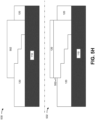
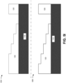
- Fig. 2 is a diagram of an example implementation of a multispectral filter 200 described herein.
- multispectral filter 200 may include a first substrate 110-1, a second substrate 110-2, a medium 120, a first mirror 130-1, a second mirror 130-2, and a spacer 140.
- second substrate 110-2 may be deposited onto second mirror 130-2.
- second mirror 130-2 may be deposited onto spacer 140, and second substrate 110-2 may be deposited onto second mirror 130-2.
- second mirror 130-2 may be deposited onto second substrate 110-2.
- medium 120 may be deposited on first substrate 110-1
- first mirror 130-1 may be deposited on medium 120
- spacer 140 may be deposited onto first mirror 130-1
- second mirror 130-2 may be deposited on second substrate 110-2
- second mirror 130-2 and second substrate 110-2 may be aligned to first mirror 130-1 and first substrate 110-1.
- Fig. 2 is provided merely as an example. Other examples are possible and may differ from what was described with regard to Fig. 2 .
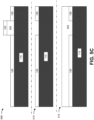
- Figs. 3A-3D are diagrams of an implementation of a multispectral filter 300 described herein but not claimed.
- multispectral filter 300 may include a first substrate 110-1, a second substrate 110-2, a medium 120, a first mirror 130-1, a second mirror 130-2, and a spacer 140.
- multispectral filter 300 is attached to one or more translation devices 310.
- second mirror 130-2 of multispectral filter 300 may be movable with respect to first mirror 130-1 to cause spacer 140 to have a variable thickness, which may alter a spectral range of light passed by channels of multispectral filter 200.
- first mirror 130-1 may be moved with respect to second mirror 130-2, both first mirror 130-1 and second mirror 130-2 may be moved by translation devices 310, and/or the like.
- second mirror 130-2 is translated by translation device 310 with respect to first mirror 130-1.
- second substrate 110-2 and second mirror 130-2 may be moved further away from first substrate 110-1 and first mirror 130-1 with respect to a position shown in Fig. 3A .
- Translation device 310 may be a focusing element, a voice-coil motor, a piezo-electric transducer, a silicon micro-electro-mechanical system (MEMS) device, a thermomechanical device, a bi-stable beam switch, and/or the like.
- MEMS micro-electro-mechanical system
- second mirror 130-2 may be translated by translation device 310 such that second mirror 130-2 is tilted with respect to first mirror 130-1.
- second substrate 110-2 may be attached to a tilting device, multiple translation devices, and/or the like.
- a wavelength range of channels of multispectral filter 300 may be further configured by reducing a separation between second mirror 130-2 and first mirror 130-1 for a first portion of channels, increasing a separation between second mirror 130-2 and first mirror 130-1 for a second portion of channels, maintaining a separation between second mirror 130-2 and first mirror 130-1 for a third portion, and/or the like.
- a movement device may move second mirror 130-2 with respect to first mirror 130-1 based on a particular timing configuration. For example, during a read-out of sensor elements aligned to channels of multispectral filter 300, the movement device may be triggered to move second mirror 130-2 to cause some channels to be associated with different wavelength ranges and other channels to maintain a default wavelength range. As an example, when a multispectral filter includes multiple channels with a common wavelength range, as shown in Figs.
- the movement device may be triggered to cause a first sensor element of a first channel associated with the common wavelength range to read out at a first position of second mirror 130-2 and a second sensor element of a second channel associated with the common wavelength range to read out at a second position of second mirror 130-2.
- the multispectral filter 200 may enable multiple spectral ranges using a common channel.
- the movement device may cause the first sensor element to read out at the first position and at the second position, resulting in capture of multiple spectral ranges using a single channel.
- Spacer 140 may be constrained to enable a variable spacer width based on translating second mirror 130-2 with respect to first mirror 130-1.
- spacer 140 may be a gaseous spacer or a liquid spacer that may be encapsulated by multispectral filter 300 to enable the gaseous spacer or the liquid spacer to expand and/or contract as second mirror 130-2 is translated with respect to first mirror 130-1.
- spacer 140 may be constrained such that additional gaseous spacer material or liquid spacer material may be provided into a gap between second mirror 130-2 and first mirror 130-1 and/or removed from the gap to enable the spacer to provide a variable thickness.
- first spacer 140-1 may be a solid spacer that covers first mirror 130-1
- second spacer 140-2 may be a gaseous (or liquid) spacer that enables a variable separation between first mirror 130-1 and second mirror 130-2.
- FIGS. 3A-3D are provided merely as examples. Other examples are possible and may differ from what was described with regard to Figs. 3A-3D .
- Fig. 4 is a flow chart of an example process 400 for manufacturing a multispectral filter described herein.
- one or more process blocks of Fig. 4 may be performed by a deposition device during a manufacturing procedure, such as by an etching device, a sputtering device, a photolithographic device, and/or the like.
- process 400 may include disposing, on a substrate, a medium to form a stepped structure (block 410).
- a deposition device may deposit the medium on the substrate to form the stepped structure.
- the deposition device may deposit multiple layers of medium to form the stepped structure.
- multiple layers of photolithographic material may be deposited and multiple layers of medium may be deposited to form the stepped structure.
- the multiple layers of photolithographic material may be exposed to light in connection with a photomask to selectively remove the photolithographic material and cause the multiple layers of medium to form the stepped structure. Photolithographic formation of the stepped structure for the medium is described in detail with regard to Figs. 5A-5K .
- the medium may be disposed on the substrate to form the stepped structure using an etching procedure.
- a medium may be deposited onto a substrate and then etched to form a stepped structure.
- process 400 may include disposing, on the medium, a first mirror for a multichannel filter to form a stepped mirror structure (block 420).
- the deposition device may deposit the first mirror on the medium.
- the first mirror forms a stepped structure based on the medium, on which the first mirror is deposited, having a stepped structure.
- process 400 may include disposing, on the first mirror, a spacer for the multichannel filter (block 430).
- the deposition device may deposit the spacer on the first mirror.
- the spacer may be a solid spacer deposited using a single deposition step, which may reduce surface layer oxidation based effects to optical performance relative to depositing the spacer using multiple deposition and etching steps.
- the spacer may be a liquid spacer or a gaseous spacer that may be inserted into a cavity formed by the first mirror and a second mirror, which may enable a variable spacer binary multispectral filter with a translatable mirror (not claimed).
- the spacer may form a flat surface.
- the spacer may be deposited onto the first mirror such that a first surface interfacing with a stepped mirror surface of the first mirror is stepped and such that a second surface on an opposite side of the spacer is flat.
- the spacer may be etched to remove a portion of the spacer to form the flat surface.
- the first mirror or the medium may form an etch stop for etching the spacer to form the flat surface.
- process 400 may include disposing, on the second surface of the spacer, a second mirror to form a flat mirror for the multichannel filter (block 440).
- the deposition device may deposit the second mirror on the second surface of the spacer such that the mirror is a flat mirror.
- the second mirror may be aligned to the first mirror.
- the second mirror may be deposited onto another substrate, and the second mirror and the other substrate may be aligned to the first mirror such that the second mirror and the other substrate are translatable with respect to the first mirror to form a variable thickness spacer (not claimed). In this way, a multispectral filter may be formed with multiple channels.
- process 400 may include additional blocks, fewer blocks, different blocks, or differently arranged blocks than those depicted in Fig. 4 . Additionally, or alternatively, two or more of the blocks of process 400 may be performed in parallel.
- Figs. 5A-5K are diagrams of an example implementation relating to process 400. Figs. 5A-5K show an example process for manufacturing a multispectral filter described herein.
- photoresist 552 may be deposited onto substrate 110. As shown by diagram 502, photomask 554 and 556 may positioned over photoresist 552.
- photomask 554 and 556 and a portion of photoresist 552 not covered by photomask 554 and 556 may be exposed to light. As shown by diagram 506, based on the exposure to light, the portion of photoresist 552 not covered by photomask 554 and 556 may remain disposed on substrate 110.
- a layer of medium 120 may be deposited onto substrate 110 and the remaining portion of photoresist 552.
- the remaining portion of photoresist 552 may be removed.
- portions of the layer of medium 120 deposited onto substrate 110 may remain, forming a first step where the remaining portion of photoresist 552 was removed.
- another layer of photoresist 552 may be deposited onto medium 120 and substrate 110.
- the other layer of photoresist 552 may be removed, resulting in medium 120 forming two steps.
- another layer of photoresist 552 may be deposited onto medium 120 and substrate 110.
- the other layer of photoresist 552 may be removed, resulting in medium 120 forming three steps.
- another layer of photoresist 552 may be deposited onto medium 120 and substrate 110.
- the other layer of photoresist 552 may be removed, resulting in medium 120 forming 4 steps.
- a set of 6 steps may be formed by medium 120 with channels at each edge of the multispectral filter being a common channel.
- a first mirror 558 may be deposited onto the set of 6 steps formed by medium 120.
- a spacer 560 may be deposited onto first mirror 558.
- a first surface of spacer 560 at an interface with first mirror 558 is stepped based on first mirror 558 having a stepped surface.
- a second surface of spacer 560 is a non-flat surface.
- an etching procedure may remove a portion of the second surface of spacer 560 to cause the second surface of spacer 560 to be a flat surface.
- a second mirror 562 is deposited on the flat second surface of spacer 560. In this case, based on the first surface being stepped and the second surface being flat, spacer 560 forms multiple channels for the multispectral filter without multiple layers of deposition for spacer 560.
- FIGS. 5A-5K are provided merely as examples. Other examples are possible and may differ from what was described with regard to Figs. 5A-5K .
- Fig. 6 is a diagram of an example implementation 600 described herein.
- example implementation 600 includes a sensor system 610.
- Sensor system 610 may be a portion of an optical system, and may provide an electrical output corresponding to a sensor determination.
- sensor system 610 may be a portion of a biometric system, a security system, a health monitoring system, an object identification system, a spectroscopic identification system, an imaging system, and/or the like.
- Sensor system 610 includes an optical filter structure 620, which includes an optical filter 630, and a set of optical sensors 640 (e.g., a sensor element array).
- optical filter structure 620 may include an optical filter 630 that performs a bandpass blocking functionality and/or the like.
- optical filter 630 may be a multispectral filter, such as a multispectral filter with a stepped medium and a monolithic spacer, a multispectral filter with a variable thickness spacer, and/or the like.
- Sensor system 610 includes an optical transmitter 650 that transmits an optical signal toward a target 660 (e.g., a person, an object, etc.).
- a target 660 e.g., a person, an object, etc.
- implementations, described herein may be described in terms of an optical filter in a sensor system, implementations described herein may be used in another type of system, may be used external to the sensor system, and/or the like.
- optical filter 630 may direct the second portion of the optical signal in another direction toward a differently located optical sensor 640.
- optical sensor 640 may be an avalanche photodiode, an Indium-Gallium-Arsenide (InGaAs) detector, an infrared detector, and/or the like.
- an input optical signal is directed toward optical filter structure 620.
- the input optical signal may include visible light, near-infrared light, mid-infrared light, and/or the like emitted by optical transmitter 650 and ambient light from the environment in which sensor system 610 is being utilized.
- optical transmitter 650 may direct multiple wavelength ranges of near-infrared light toward an object for a spectroscopic measurement, and the near-infrared light may be reflected off target 660 (e.g., the object) toward optical sensors 640 to permit optical sensors 640 to perform a measurement of the multiple wavelength ranges of near-infrared light.
- ambient light may be directed toward optical sensor 640 from one or more ambient light sources (e.g., a light bulb or the sun).
- multiple light beams may be directed toward target 660 and a subset of the multiple light beams may be reflected toward optical filter structure 620, which may be disposed at a tilt angle relative to optical sensor 640, as shown. In some implementations, another tilt angle may be used.
- optical filter structure 620 may be disposed and/or formed directly onto optical sensors 640, disposed a distance from optical sensors 640 (e.g., via free-space optics), and/or the like.
- optical filter structure 620 may be coated and patterned onto optical sensors 640 using, for example, photolithography, a sputter deposition technique (e.g., using argon gas and helium gas as an inert gas mixture for sputter deposition), and/or the like.
- a sputter deposition technique e.g., using argon gas and helium gas as an inert gas mixture for sputter deposition
- optical transmitter 650 may direct near-infrared light toward another type of target 660, such as for detecting a gesture in a gesture recognition system, detecting objects in proximity to a vehicle, detecting objects in proximity to a blind person, detecting a proximity to an object (e.g., using a LIDAR technique), and/or the like, and the near-infrared light and ambient light may be directed toward optical sensor 640 as a result.
- target 660 such as for detecting a gesture in a gesture recognition system, detecting objects in proximity to a vehicle, detecting objects in proximity to a blind person, detecting a proximity to an object (e.g., using a LIDAR technique), and/or the like, and the near-infrared light and ambient light may be directed toward optical sensor 640 as a result.
- a portion of the optical signal is passed by optical filter 630 and optical filter structure 620.
- differing spacer thicknesses of different channels of optical filter 630 may cause a first portion of light to be reflected and a second portion of light to be passed.
- optical filter 630 may include multiple channels formed by a spacer in connection with a stepped medium and each channel may pass a different wavelength of light. Additionally, or alternatively, two or more channels may pass a common wavelength of light.
- optical sensor 640 may provide an output electrical signal for sensor system 610, such as for use in performing a spectroscopic measurement, recognizing a gesture of the user, detecting the presence of an object, and/or the like.
- Fig. 6 is provided merely as an example. Other examples are possible and may differ from what was described with regard to Fig. 6 .
- satisfying a threshold may refer to a value being greater than the threshold, more than the threshold, higher than the threshold, greater than or equal to the threshold, less than the threshold, fewer than the threshold, lower than the threshold, less than or equal to the threshold, equal to the threshold, and/or the like.
Landscapes
- Physics & Mathematics (AREA)
- General Physics & Mathematics (AREA)
- Optics & Photonics (AREA)
- Spectroscopy & Molecular Physics (AREA)
- Spectrometry And Color Measurement (AREA)
- Optical Filters (AREA)
- Instruments For Measurement Of Length By Optical Means (AREA)
- Mounting And Adjusting Of Optical Elements (AREA)
- Solid State Image Pick-Up Elements (AREA)
- Investigating Or Analysing Materials By Optical Means (AREA)
Applications Claiming Priority (1)
| Application Number | Priority Date | Filing Date | Title |
|---|---|---|---|
| US16/179,480 US10962694B2 (en) | 2018-11-02 | 2018-11-02 | Stepped structure optical filter |
Publications (3)
| Publication Number | Publication Date |
|---|---|
| EP3647839A2 EP3647839A2 (en) | 2020-05-06 |
| EP3647839A3 EP3647839A3 (en) | 2020-07-29 |
| EP3647839B1 true EP3647839B1 (en) | 2024-10-30 |
Family
ID=68426196
Family Applications (1)
| Application Number | Title | Priority Date | Filing Date |
|---|---|---|---|
| EP19206709.8A Active EP3647839B1 (en) | 2018-11-02 | 2019-11-01 | Stepped structure optical filter |
Country Status (7)
| Country | Link |
|---|---|
| US (3) | US10962694B2 (https=) |
| EP (1) | EP3647839B1 (https=) |
| JP (3) | JP7210417B2 (https=) |
| KR (2) | KR102565869B1 (https=) |
| CN (2) | CN117031607A (https=) |
| CA (1) | CA3060740A1 (https=) |
| TW (2) | TWI907760B (https=) |
Families Citing this family (13)
| Publication number | Priority date | Publication date | Assignee | Title |
|---|---|---|---|---|
| US10962694B2 (en) | 2018-11-02 | 2021-03-30 | Viavi Solutions Inc. | Stepped structure optical filter |
| US12392945B2 (en) * | 2020-04-28 | 2025-08-19 | Viavi Solutions Inc. | Induced transmission filter with hydrogenated silicon, silver, and silicon dioxide |
| CN111579067B (zh) * | 2020-05-22 | 2023-03-03 | 中国科学院上海技术物理研究所 | 一种具有超宽带外截止的集成窄带分光器件 |
| CN113767309A (zh) * | 2020-05-28 | 2021-12-07 | 深圳市海谱纳米光学科技有限公司 | 一种可调光学滤波器件和光谱成像系统 |
| EP3943988B1 (en) | 2020-07-20 | 2023-12-27 | Samsung Electronics Co., Ltd. | Spectral filter, and image sensor and electronic device including the spectral filter |
| WO2022147920A1 (zh) * | 2021-01-11 | 2022-07-14 | 苏州联讯仪器有限公司 | 用于光通信的光波长测量系统 |
| CN113503978A (zh) * | 2021-08-16 | 2021-10-15 | 苏州联讯仪器有限公司 | 光通信用光波长测量系统 |
| KR102727382B1 (ko) * | 2021-08-27 | 2024-11-07 | 경북대학교 산학협력단 | 마이크로옵틱 마하젠더 간섭계의 파장대역 특성을 원하는 형상으로 제어하는 방법 |
| WO2023027523A1 (ko) * | 2021-08-27 | 2023-03-02 | 경북대학교 산학협력단 | 마이크로옵틱 마하젠더 간섭계의 파장대역 특성을 원하는 형상으로 제어하는 방법 |
| CN114236663B (zh) * | 2021-12-15 | 2025-07-25 | 浙江大学 | 大面积单片集成的平坦化多通道滤光片阵列及制备方法 |
| CN114551489A (zh) * | 2022-02-11 | 2022-05-27 | 中国科学院上海技术物理研究所 | 一种分光与探测一体化的短波红外光谱探测器 |
| CN115831041B (zh) * | 2023-01-09 | 2023-04-18 | 北京数字光芯集成电路设计有限公司 | 一种阶梯式线阵MicroLED、扫描装置及扫描方法 |
| CN119779483A (zh) * | 2025-01-23 | 2025-04-08 | 星遥光宇(常州)科技有限公司 | 多光谱成像系统的焦面补偿方法、焦面补偿系统 |
Citations (1)
| Publication number | Priority date | Publication date | Assignee | Title |
|---|---|---|---|---|
| US20120326430A1 (en) * | 2011-06-23 | 2012-12-27 | Jds Uniphase Corporation | Multi color-shifting devices |
Family Cites Families (31)
| Publication number | Priority date | Publication date | Assignee | Title |
|---|---|---|---|---|
| JPS5920804A (ja) | 1982-07-28 | 1984-02-02 | Minolta Camera Co Ltd | 膜厚監視装置 |
| JPH0814509B2 (ja) * | 1986-05-15 | 1996-02-14 | ミノルタ株式会社 | 分光測定センサ |
| JP3375147B2 (ja) | 1992-05-26 | 2003-02-10 | 浜松ホトニクス株式会社 | 半導体光検出装置 |
| WO1995017690A1 (en) * | 1993-12-23 | 1995-06-29 | Honeywell Inc. | Color filter array |
| JPH1138397A (ja) * | 1997-07-24 | 1999-02-12 | Sharp Corp | 反射型カラー液晶表示素子 |
| CA2211655C (en) * | 1997-07-28 | 2003-01-07 | Paul Colbourne | Multi-pass etalon filter |
| JP4862008B2 (ja) * | 1999-02-15 | 2012-01-25 | シャープ株式会社 | 液晶表示装置 |
| US6791736B2 (en) * | 2001-06-19 | 2004-09-14 | Teralum Llc | Optical device for dispersion compensation |
| JP2004287191A (ja) * | 2003-03-24 | 2004-10-14 | Seiko Epson Corp | カラーフィルタアレイおよび空間光変調装置および投射型表示装置 |
| KR100617039B1 (ko) * | 2004-02-26 | 2006-08-30 | 엘지.필립스 엘시디 주식회사 | 액정 표시 장치 및 이의 제조 방법 |
| FR2904432B1 (fr) | 2006-07-25 | 2008-10-24 | Commissariat Energie Atomique | Structure matricielle de filtrage optique et capteur d'images associe |
| EP2057446A2 (de) | 2006-08-09 | 2009-05-13 | Opsolution Nanophotonics GmbH | Optisches filter und verfahren zur herstellung desselben, sowie vorrichtung zur untersuchung elektromagnetischer strahlung |
| US7803704B2 (en) * | 2008-08-22 | 2010-09-28 | Chartered Semiconductor Manufacturing, Ltd. | Reliable interconnects |
| JP2010113058A (ja) * | 2008-11-05 | 2010-05-20 | Seiko Epson Corp | カラーフィルターの製造方法、カラーフィルター、画像表示装置、および、電子機器 |
| KR20120030547A (ko) | 2009-06-17 | 2012-03-28 | 코닌클리즈케 필립스 일렉트로닉스 엔.브이. | 미니 분광계를 위한 고투과 및 큰 저지 범위를 갖는 간섭 필터 |
| KR101494951B1 (ko) | 2010-01-21 | 2015-02-23 | 가부시끼가이샤 도시바 | 간섭형 필터층 부착 기판 및 그것을 사용한 표시 장치 |
| US20120200852A1 (en) * | 2010-09-10 | 2012-08-09 | Aerospace Missions Corporation | Spectroscopy and spectral imaging methods and apparatus |
| CN102798917B (zh) * | 2011-05-25 | 2015-02-25 | 苏州大学 | 一种彩色图像制作方法及使用该方法制作的彩色滤光片 |
| JP5757835B2 (ja) * | 2011-10-04 | 2015-08-05 | 浜松ホトニクス株式会社 | 分光センサの製造方法 |
| CN102832237B (zh) * | 2012-07-03 | 2015-04-01 | 电子科技大学 | 一种槽型半导体功率器件 |
| US20160182786A1 (en) | 2013-09-11 | 2016-06-23 | Lytro, Inc. | Hybrid light-field camera |
| FR3020878B1 (fr) * | 2014-05-06 | 2025-06-06 | Commissariat Energie Atomique | Dispositif de filtrage optique comportant des cavites fabry-perot a couche structuree et d'epaisseurs differentes |
| US9823395B2 (en) * | 2014-10-17 | 2017-11-21 | 3M Innovative Properties Company | Multilayer optical film having overlapping harmonics |
| CN105093376A (zh) * | 2015-09-07 | 2015-11-25 | 西安工业大学 | 中心波长渐变的带通滤光片制备方法 |
| US9960199B2 (en) | 2015-12-29 | 2018-05-01 | Viavi Solutions Inc. | Dielectric mirror based multispectral filter array |
| JP2017168822A (ja) * | 2016-02-12 | 2017-09-21 | ヴァイアヴィ・ソリューションズ・インコーポレイテッドViavi Solutions Inc. | センサデバイスの製造方法 |
| US10170509B2 (en) * | 2016-02-12 | 2019-01-01 | Viavi Solutions Inc. | Optical filter array |
| DE102016010078A1 (de) | 2016-08-18 | 2018-02-22 | Giesecke+Devrient Currency Technology Gmbh | Optisch variables Sicherheitselement mit Dünnschichtelement |
| EP3324161B1 (de) | 2016-11-18 | 2020-06-17 | Espros Photonics AG | Spektrometer und verfahren zur justierung eines filterarrays |
| US10914961B2 (en) | 2017-02-13 | 2021-02-09 | Viavi Solutions Inc. | Optical polarizing filter |
| US10962694B2 (en) | 2018-11-02 | 2021-03-30 | Viavi Solutions Inc. | Stepped structure optical filter |
-
2018
- 2018-11-02 US US16/179,480 patent/US10962694B2/en active Active
-
2019
- 2019-10-29 CA CA3060740A patent/CA3060740A1/en active Pending
- 2019-10-31 KR KR1020190137902A patent/KR102565869B1/ko active Active
- 2019-10-31 TW TW111149950A patent/TWI907760B/zh active
- 2019-10-31 TW TW108139486A patent/TWI791917B/zh active
- 2019-11-01 JP JP2019199619A patent/JP7210417B2/ja active Active
- 2019-11-01 EP EP19206709.8A patent/EP3647839B1/en active Active
- 2019-11-04 CN CN202311061226.8A patent/CN117031607A/zh active Pending
- 2019-11-04 CN CN201911067451.6A patent/CN111142179B/zh active Active
-
2021
- 2021-03-17 US US17/249,872 patent/US11892664B2/en active Active
-
2023
- 2023-01-11 JP JP2023002173A patent/JP7822974B2/ja active Active
- 2023-08-07 KR KR1020230102639A patent/KR102951105B1/ko active Active
- 2023-11-30 US US18/523,975 patent/US12436328B2/en active Active
-
2024
- 2024-09-06 JP JP2024153647A patent/JP2024174959A/ja active Pending
Patent Citations (1)
| Publication number | Priority date | Publication date | Assignee | Title |
|---|---|---|---|---|
| US20120326430A1 (en) * | 2011-06-23 | 2012-12-27 | Jds Uniphase Corporation | Multi color-shifting devices |
Also Published As
| Publication number | Publication date |
|---|---|
| TWI791917B (zh) | 2023-02-11 |
| EP3647839A2 (en) | 2020-05-06 |
| JP2023052306A (ja) | 2023-04-11 |
| US20200142111A1 (en) | 2020-05-07 |
| JP2024174959A (ja) | 2024-12-17 |
| EP3647839A3 (en) | 2020-07-29 |
| US20210199866A1 (en) | 2021-07-01 |
| JP7822974B2 (ja) | 2026-03-03 |
| US11892664B2 (en) | 2024-02-06 |
| KR20200050882A (ko) | 2020-05-12 |
| JP2020071488A (ja) | 2020-05-07 |
| KR102951105B1 (ko) | 2026-04-09 |
| US20240094450A1 (en) | 2024-03-21 |
| KR20230118795A (ko) | 2023-08-14 |
| CN117031607A (zh) | 2023-11-10 |
| CA3060740A1 (en) | 2020-05-02 |
| US10962694B2 (en) | 2021-03-30 |
| CN111142179B (zh) | 2023-09-08 |
| CN111142179A (zh) | 2020-05-12 |
| TWI907760B (zh) | 2025-12-11 |
| TW202024680A (zh) | 2020-07-01 |
| JP7210417B2 (ja) | 2023-01-23 |
| US12436328B2 (en) | 2025-10-07 |
| KR102565869B1 (ko) | 2023-08-10 |
| TW202316146A (zh) | 2023-04-16 |
Similar Documents
| Publication | Publication Date | Title |
|---|---|---|
| EP3647839B1 (en) | Stepped structure optical filter | |
| EP3187910B1 (en) | Dielectric mirror based multispectral filter array | |
| US20190187347A1 (en) | Optical filters | |
| EP3495789B1 (en) | Multispectral sensor response balancing | |
| KR20200013617A (ko) | 다중 스펙트럼 필터 | |
| HK40093250A (zh) | 阶梯结构光滤波器 | |
| HK40019338B (zh) | 阶梯结构光滤波器 | |
| HK40019338A (en) | Stepped structure optical filter | |
| TW202609359A (zh) | 階梯式結構光學濾波器 | |
| EP4682594A1 (en) | Zero angle shift bandpass filter | |
| EP4485018A1 (en) | Angle selective filter | |
| HK40110693A (zh) | 光学干涉滤波器 | |
| HK40002319A (en) | Optical filters | |
| HK40001995A (en) | Multispectral sensor response balancing |
Legal Events
| Date | Code | Title | Description |
|---|---|---|---|
| PUAI | Public reference made under article 153(3) epc to a published international application that has entered the european phase |
Free format text: ORIGINAL CODE: 0009012 |
|
| STAA | Information on the status of an ep patent application or granted ep patent |
Free format text: STATUS: THE APPLICATION HAS BEEN PUBLISHED |
|
| AK | Designated contracting states |
Kind code of ref document: A2 Designated state(s): AL AT BE BG CH CY CZ DE DK EE ES FI FR GB GR HR HU IE IS IT LI LT LU LV MC MK MT NL NO PL PT RO RS SE SI SK SM TR |
|
| AX | Request for extension of the european patent |
Extension state: BA ME |
|
| PUAL | Search report despatched |
Free format text: ORIGINAL CODE: 0009013 |
|
| AK | Designated contracting states |
Kind code of ref document: A3 Designated state(s): AL AT BE BG CH CY CZ DE DK EE ES FI FR GB GR HR HU IE IS IT LI LT LU LV MC MK MT NL NO PL PT RO RS SE SI SK SM TR |
|
| AX | Request for extension of the european patent |
Extension state: BA ME |
|
| RIC1 | Information provided on ipc code assigned before grant |
Ipc: G02B 26/00 20060101ALI20200623BHEP Ipc: G02B 5/28 20060101AFI20200623BHEP |
|
| STAA | Information on the status of an ep patent application or granted ep patent |
Free format text: STATUS: REQUEST FOR EXAMINATION WAS MADE |
|
| 17P | Request for examination filed |
Effective date: 20210126 |
|
| RBV | Designated contracting states (corrected) |
Designated state(s): AL AT BE BG CH CY CZ DE DK EE ES FI FR GB GR HR HU IE IS IT LI LT LU LV MC MK MT NL NO PL PT RO RS SE SI SK SM TR |
|
| STAA | Information on the status of an ep patent application or granted ep patent |
Free format text: STATUS: EXAMINATION IS IN PROGRESS |
|
| 17Q | First examination report despatched |
Effective date: 20220315 |
|
| RAP3 | Party data changed (applicant data changed or rights of an application transferred) |
Owner name: VIAVI SOLUTIONS INC. |
|
| P01 | Opt-out of the competence of the unified patent court (upc) registered |
Effective date: 20230530 |
|
| GRAP | Despatch of communication of intention to grant a patent |
Free format text: ORIGINAL CODE: EPIDOSNIGR1 |
|
| STAA | Information on the status of an ep patent application or granted ep patent |
Free format text: STATUS: GRANT OF PATENT IS INTENDED |
|
| INTG | Intention to grant announced |
Effective date: 20240522 |
|
| GRAS | Grant fee paid |
Free format text: ORIGINAL CODE: EPIDOSNIGR3 |
|
| GRAA | (expected) grant |
Free format text: ORIGINAL CODE: 0009210 |
|
| STAA | Information on the status of an ep patent application or granted ep patent |
Free format text: STATUS: THE PATENT HAS BEEN GRANTED |
|
| AK | Designated contracting states |
Kind code of ref document: B1 Designated state(s): AL AT BE BG CH CY CZ DE DK EE ES FI FR GB GR HR HU IE IS IT LI LT LU LV MC MK MT NL NO PL PT RO RS SE SI SK SM TR |
|
| REG | Reference to a national code |
Ref country code: GB Ref legal event code: FG4D |
|
| REG | Reference to a national code |
Ref country code: CH Ref legal event code: EP |
|
| REG | Reference to a national code |
Ref country code: DE Ref legal event code: R096 Ref document number: 602019061061 Country of ref document: DE |
|
| REG | Reference to a national code |
Ref country code: IE Ref legal event code: FG4D |
|
| REG | Reference to a national code |
Ref country code: LT Ref legal event code: MG9D |
|
| REG | Reference to a national code |
Ref country code: NL Ref legal event code: MP Effective date: 20241030 |
|
| PG25 | Lapsed in a contracting state [announced via postgrant information from national office to epo] |
Ref country code: HR Free format text: LAPSE BECAUSE OF FAILURE TO SUBMIT A TRANSLATION OF THE DESCRIPTION OR TO PAY THE FEE WITHIN THE PRESCRIBED TIME-LIMIT Effective date: 20241030 Ref country code: IS Free format text: LAPSE BECAUSE OF FAILURE TO SUBMIT A TRANSLATION OF THE DESCRIPTION OR TO PAY THE FEE WITHIN THE PRESCRIBED TIME-LIMIT Effective date: 20250228 Ref country code: PT Free format text: LAPSE BECAUSE OF FAILURE TO SUBMIT A TRANSLATION OF THE DESCRIPTION OR TO PAY THE FEE WITHIN THE PRESCRIBED TIME-LIMIT Effective date: 20250228 |
|
| PG25 | Lapsed in a contracting state [announced via postgrant information from national office to epo] |
Ref country code: FI Free format text: LAPSE BECAUSE OF FAILURE TO SUBMIT A TRANSLATION OF THE DESCRIPTION OR TO PAY THE FEE WITHIN THE PRESCRIBED TIME-LIMIT Effective date: 20241030 Ref country code: NL Free format text: LAPSE BECAUSE OF FAILURE TO SUBMIT A TRANSLATION OF THE DESCRIPTION OR TO PAY THE FEE WITHIN THE PRESCRIBED TIME-LIMIT Effective date: 20241030 |
|
| REG | Reference to a national code |
Ref country code: AT Ref legal event code: MK05 Ref document number: 1737427 Country of ref document: AT Kind code of ref document: T Effective date: 20241030 |
|
| PG25 | Lapsed in a contracting state [announced via postgrant information from national office to epo] |
Ref country code: BG Free format text: LAPSE BECAUSE OF FAILURE TO SUBMIT A TRANSLATION OF THE DESCRIPTION OR TO PAY THE FEE WITHIN THE PRESCRIBED TIME-LIMIT Effective date: 20241030 |
|
| PG25 | Lapsed in a contracting state [announced via postgrant information from national office to epo] |
Ref country code: ES Free format text: LAPSE BECAUSE OF FAILURE TO SUBMIT A TRANSLATION OF THE DESCRIPTION OR TO PAY THE FEE WITHIN THE PRESCRIBED TIME-LIMIT Effective date: 20241030 |
|
| PG25 | Lapsed in a contracting state [announced via postgrant information from national office to epo] |
Ref country code: NO Free format text: LAPSE BECAUSE OF FAILURE TO SUBMIT A TRANSLATION OF THE DESCRIPTION OR TO PAY THE FEE WITHIN THE PRESCRIBED TIME-LIMIT Effective date: 20250130 |
|
| PG25 | Lapsed in a contracting state [announced via postgrant information from national office to epo] |
Ref country code: LV Free format text: LAPSE BECAUSE OF FAILURE TO SUBMIT A TRANSLATION OF THE DESCRIPTION OR TO PAY THE FEE WITHIN THE PRESCRIBED TIME-LIMIT Effective date: 20241030 Ref country code: AT Free format text: LAPSE BECAUSE OF FAILURE TO SUBMIT A TRANSLATION OF THE DESCRIPTION OR TO PAY THE FEE WITHIN THE PRESCRIBED TIME-LIMIT Effective date: 20241030 Ref country code: GR Free format text: LAPSE BECAUSE OF FAILURE TO SUBMIT A TRANSLATION OF THE DESCRIPTION OR TO PAY THE FEE WITHIN THE PRESCRIBED TIME-LIMIT Effective date: 20250131 |
|
| PG25 | Lapsed in a contracting state [announced via postgrant information from national office to epo] |
Ref country code: PL Free format text: LAPSE BECAUSE OF FAILURE TO SUBMIT A TRANSLATION OF THE DESCRIPTION OR TO PAY THE FEE WITHIN THE PRESCRIBED TIME-LIMIT Effective date: 20241030 |
|
| PG25 | Lapsed in a contracting state [announced via postgrant information from national office to epo] |
Ref country code: RS Free format text: LAPSE BECAUSE OF FAILURE TO SUBMIT A TRANSLATION OF THE DESCRIPTION OR TO PAY THE FEE WITHIN THE PRESCRIBED TIME-LIMIT Effective date: 20250130 |
|
| PG25 | Lapsed in a contracting state [announced via postgrant information from national office to epo] |
Ref country code: SM Free format text: LAPSE BECAUSE OF FAILURE TO SUBMIT A TRANSLATION OF THE DESCRIPTION OR TO PAY THE FEE WITHIN THE PRESCRIBED TIME-LIMIT Effective date: 20241030 |
|
| PG25 | Lapsed in a contracting state [announced via postgrant information from national office to epo] |
Ref country code: MC Free format text: LAPSE BECAUSE OF FAILURE TO SUBMIT A TRANSLATION OF THE DESCRIPTION OR TO PAY THE FEE WITHIN THE PRESCRIBED TIME-LIMIT Effective date: 20241030 |
|
| PG25 | Lapsed in a contracting state [announced via postgrant information from national office to epo] |
Ref country code: DK Free format text: LAPSE BECAUSE OF FAILURE TO SUBMIT A TRANSLATION OF THE DESCRIPTION OR TO PAY THE FEE WITHIN THE PRESCRIBED TIME-LIMIT Effective date: 20241030 |
|
| PG25 | Lapsed in a contracting state [announced via postgrant information from national office to epo] |
Ref country code: LU Free format text: LAPSE BECAUSE OF NON-PAYMENT OF DUE FEES Effective date: 20241101 |
|
| PG25 | Lapsed in a contracting state [announced via postgrant information from national office to epo] |
Ref country code: EE Free format text: LAPSE BECAUSE OF FAILURE TO SUBMIT A TRANSLATION OF THE DESCRIPTION OR TO PAY THE FEE WITHIN THE PRESCRIBED TIME-LIMIT Effective date: 20241030 |
|
| PG25 | Lapsed in a contracting state [announced via postgrant information from national office to epo] |
Ref country code: RO Free format text: LAPSE BECAUSE OF FAILURE TO SUBMIT A TRANSLATION OF THE DESCRIPTION OR TO PAY THE FEE WITHIN THE PRESCRIBED TIME-LIMIT Effective date: 20241030 |
|
| PG25 | Lapsed in a contracting state [announced via postgrant information from national office to epo] |
Ref country code: SK Free format text: LAPSE BECAUSE OF FAILURE TO SUBMIT A TRANSLATION OF THE DESCRIPTION OR TO PAY THE FEE WITHIN THE PRESCRIBED TIME-LIMIT Effective date: 20241030 |
|
| PG25 | Lapsed in a contracting state [announced via postgrant information from national office to epo] |
Ref country code: CZ Free format text: LAPSE BECAUSE OF FAILURE TO SUBMIT A TRANSLATION OF THE DESCRIPTION OR TO PAY THE FEE WITHIN THE PRESCRIBED TIME-LIMIT Effective date: 20241030 |
|
| PG25 | Lapsed in a contracting state [announced via postgrant information from national office to epo] |
Ref country code: IT Free format text: LAPSE BECAUSE OF FAILURE TO SUBMIT A TRANSLATION OF THE DESCRIPTION OR TO PAY THE FEE WITHIN THE PRESCRIBED TIME-LIMIT Effective date: 20241030 |
|
| REG | Reference to a national code |
Ref country code: DE Ref legal event code: R097 Ref document number: 602019061061 Country of ref document: DE |
|
| REG | Reference to a national code |
Ref country code: BE Ref legal event code: MM Effective date: 20241130 |
|
| PLBE | No opposition filed within time limit |
Free format text: ORIGINAL CODE: 0009261 |
|
| STAA | Information on the status of an ep patent application or granted ep patent |
Free format text: STATUS: NO OPPOSITION FILED WITHIN TIME LIMIT |
|
| PG25 | Lapsed in a contracting state [announced via postgrant information from national office to epo] |
Ref country code: SE Free format text: LAPSE BECAUSE OF FAILURE TO SUBMIT A TRANSLATION OF THE DESCRIPTION OR TO PAY THE FEE WITHIN THE PRESCRIBED TIME-LIMIT Effective date: 20241030 |
|
| 26N | No opposition filed |
Effective date: 20250731 |
|
| PG25 | Lapsed in a contracting state [announced via postgrant information from national office to epo] |
Ref country code: BE Free format text: LAPSE BECAUSE OF NON-PAYMENT OF DUE FEES Effective date: 20241130 |
|
| PG25 | Lapsed in a contracting state [announced via postgrant information from national office to epo] |
Ref country code: IE Free format text: LAPSE BECAUSE OF NON-PAYMENT OF DUE FEES Effective date: 20241101 |
|
| REG | Reference to a national code |
Ref country code: CH Ref legal event code: U11 Free format text: ST27 STATUS EVENT CODE: U-0-0-U10-U11 (AS PROVIDED BY THE NATIONAL OFFICE) Effective date: 20251201 |
|
| PGFP | Annual fee paid to national office [announced via postgrant information from national office to epo] |
Ref country code: DE Payment date: 20251127 Year of fee payment: 7 |
|
| PGFP | Annual fee paid to national office [announced via postgrant information from national office to epo] |
Ref country code: GB Payment date: 20251128 Year of fee payment: 7 |
|
| PGFP | Annual fee paid to national office [announced via postgrant information from national office to epo] |
Ref country code: FR Payment date: 20251127 Year of fee payment: 7 |
|
| PGFP | Annual fee paid to national office [announced via postgrant information from national office to epo] |
Ref country code: CH Payment date: 20251201 Year of fee payment: 7 |