EP3637176B1 - Lichtsteuervorrichtung - Google Patents
Lichtsteuervorrichtung Download PDFInfo
- Publication number
- EP3637176B1 EP3637176B1 EP18812822.7A EP18812822A EP3637176B1 EP 3637176 B1 EP3637176 B1 EP 3637176B1 EP 18812822 A EP18812822 A EP 18812822A EP 3637176 B1 EP3637176 B1 EP 3637176B1
- Authority
- EP
- European Patent Office
- Prior art keywords
- voltage
- terminal
- light control
- period
- signal
- Prior art date
- Legal status (The legal status is an assumption and is not a legal conclusion. Google has not performed a legal analysis and makes no representation as to the accuracy of the status listed.)
- Active
Links
- 239000004973 liquid crystal related substance Substances 0.000 claims description 77
- 238000010586 diagram Methods 0.000 description 18
- 239000000463 material Substances 0.000 description 15
- 229920000642 polymer Polymers 0.000 description 12
- 238000002834 transmittance Methods 0.000 description 12
- 230000000052 comparative effect Effects 0.000 description 9
- 239000002861 polymer material Substances 0.000 description 8
- 239000004983 Polymer Dispersed Liquid Crystal Substances 0.000 description 7
- 239000011159 matrix material Substances 0.000 description 7
- 238000000034 method Methods 0.000 description 7
- 230000007423 decrease Effects 0.000 description 3
- 230000005684 electric field Effects 0.000 description 3
- 239000004698 Polyethylene Substances 0.000 description 2
- 230000005540 biological transmission Effects 0.000 description 2
- 239000000178 monomer Substances 0.000 description 2
- 229920000573 polyethylene Polymers 0.000 description 2
- -1 polyethylene terephthalate Polymers 0.000 description 2
- 229920000139 polyethylene terephthalate Polymers 0.000 description 2
- 239000005020 polyethylene terephthalate Substances 0.000 description 2
- 239000011347 resin Substances 0.000 description 2
- 229920005989 resin Polymers 0.000 description 2
- 239000004065 semiconductor Substances 0.000 description 2
- RYGMFSIKBFXOCR-UHFFFAOYSA-N Copper Chemical compound [Cu] RYGMFSIKBFXOCR-UHFFFAOYSA-N 0.000 description 1
- JMASRVWKEDWRBT-UHFFFAOYSA-N Gallium nitride Chemical compound [Ga]#N JMASRVWKEDWRBT-UHFFFAOYSA-N 0.000 description 1
- 239000004988 Nematic liquid crystal Substances 0.000 description 1
- BQCADISMDOOEFD-UHFFFAOYSA-N Silver Chemical compound [Ag] BQCADISMDOOEFD-UHFFFAOYSA-N 0.000 description 1
- 238000010521 absorption reaction Methods 0.000 description 1
- 229910052782 aluminium Inorganic materials 0.000 description 1
- XAGFODPZIPBFFR-UHFFFAOYSA-N aluminium Chemical compound [Al] XAGFODPZIPBFFR-UHFFFAOYSA-N 0.000 description 1
- 230000003321 amplification Effects 0.000 description 1
- 229910052802 copper Inorganic materials 0.000 description 1
- 239000010949 copper Substances 0.000 description 1
- 230000000694 effects Effects 0.000 description 1
- PCHJSUWPFVWCPO-UHFFFAOYSA-N gold Chemical compound [Au] PCHJSUWPFVWCPO-UHFFFAOYSA-N 0.000 description 1
- 229910052737 gold Inorganic materials 0.000 description 1
- 239000010931 gold Substances 0.000 description 1
- AMGQUBHHOARCQH-UHFFFAOYSA-N indium;oxotin Chemical compound [In].[Sn]=O AMGQUBHHOARCQH-UHFFFAOYSA-N 0.000 description 1
- 229910052751 metal Inorganic materials 0.000 description 1
- 239000002184 metal Substances 0.000 description 1
- 238000003199 nucleic acid amplification method Methods 0.000 description 1
- 238000005192 partition Methods 0.000 description 1
- 239000004417 polycarbonate Substances 0.000 description 1
- 229920000515 polycarbonate Polymers 0.000 description 1
- 239000002243 precursor Substances 0.000 description 1
- 230000003252 repetitive effect Effects 0.000 description 1
- HBMJWWWQQXIZIP-UHFFFAOYSA-N silicon carbide Chemical compound [Si+]#[C-] HBMJWWWQQXIZIP-UHFFFAOYSA-N 0.000 description 1
- 229910052709 silver Inorganic materials 0.000 description 1
- 239000004332 silver Substances 0.000 description 1
Images


Classifications
-
- G—PHYSICS
- G02—OPTICS
- G02F—OPTICAL DEVICES OR ARRANGEMENTS FOR THE CONTROL OF LIGHT BY MODIFICATION OF THE OPTICAL PROPERTIES OF THE MEDIA OF THE ELEMENTS INVOLVED THEREIN; NON-LINEAR OPTICS; FREQUENCY-CHANGING OF LIGHT; OPTICAL LOGIC ELEMENTS; OPTICAL ANALOGUE/DIGITAL CONVERTERS
- G02F1/00—Devices or arrangements for the control of the intensity, colour, phase, polarisation or direction of light arriving from an independent light source, e.g. switching, gating or modulating; Non-linear optics
- G02F1/01—Devices or arrangements for the control of the intensity, colour, phase, polarisation or direction of light arriving from an independent light source, e.g. switching, gating or modulating; Non-linear optics for the control of the intensity, phase, polarisation or colour
- G02F1/13—Devices or arrangements for the control of the intensity, colour, phase, polarisation or direction of light arriving from an independent light source, e.g. switching, gating or modulating; Non-linear optics for the control of the intensity, phase, polarisation or colour based on liquid crystals, e.g. single liquid crystal display cells
- G02F1/133—Constructional arrangements; Operation of liquid crystal cells; Circuit arrangements
- G02F1/13306—Circuit arrangements or driving methods for the control of single liquid crystal cells
-
- G—PHYSICS
- G02—OPTICS
- G02F—OPTICAL DEVICES OR ARRANGEMENTS FOR THE CONTROL OF LIGHT BY MODIFICATION OF THE OPTICAL PROPERTIES OF THE MEDIA OF THE ELEMENTS INVOLVED THEREIN; NON-LINEAR OPTICS; FREQUENCY-CHANGING OF LIGHT; OPTICAL LOGIC ELEMENTS; OPTICAL ANALOGUE/DIGITAL CONVERTERS
- G02F1/00—Devices or arrangements for the control of the intensity, colour, phase, polarisation or direction of light arriving from an independent light source, e.g. switching, gating or modulating; Non-linear optics
- G02F1/01—Devices or arrangements for the control of the intensity, colour, phase, polarisation or direction of light arriving from an independent light source, e.g. switching, gating or modulating; Non-linear optics for the control of the intensity, phase, polarisation or colour
- G02F1/13—Devices or arrangements for the control of the intensity, colour, phase, polarisation or direction of light arriving from an independent light source, e.g. switching, gating or modulating; Non-linear optics for the control of the intensity, phase, polarisation or colour based on liquid crystals, e.g. single liquid crystal display cells
- G02F1/133—Constructional arrangements; Operation of liquid crystal cells; Circuit arrangements
- G02F1/1333—Constructional arrangements; Manufacturing methods
- G02F1/1334—Constructional arrangements; Manufacturing methods based on polymer dispersed liquid crystals, e.g. microencapsulated liquid crystals
-
- G—PHYSICS
- G02—OPTICS
- G02F—OPTICAL DEVICES OR ARRANGEMENTS FOR THE CONTROL OF LIGHT BY MODIFICATION OF THE OPTICAL PROPERTIES OF THE MEDIA OF THE ELEMENTS INVOLVED THEREIN; NON-LINEAR OPTICS; FREQUENCY-CHANGING OF LIGHT; OPTICAL LOGIC ELEMENTS; OPTICAL ANALOGUE/DIGITAL CONVERTERS
- G02F1/00—Devices or arrangements for the control of the intensity, colour, phase, polarisation or direction of light arriving from an independent light source, e.g. switching, gating or modulating; Non-linear optics
- G02F1/01—Devices or arrangements for the control of the intensity, colour, phase, polarisation or direction of light arriving from an independent light source, e.g. switching, gating or modulating; Non-linear optics for the control of the intensity, phase, polarisation or colour
- G02F1/13—Devices or arrangements for the control of the intensity, colour, phase, polarisation or direction of light arriving from an independent light source, e.g. switching, gating or modulating; Non-linear optics for the control of the intensity, phase, polarisation or colour based on liquid crystals, e.g. single liquid crystal display cells
- G02F1/133—Constructional arrangements; Operation of liquid crystal cells; Circuit arrangements
- G02F1/1333—Constructional arrangements; Manufacturing methods
- G02F1/1343—Electrodes
- G02F1/13439—Electrodes characterised by their electrical, optical, physical properties; materials therefor; method of making
-
- G—PHYSICS
- G02—OPTICS
- G02F—OPTICAL DEVICES OR ARRANGEMENTS FOR THE CONTROL OF LIGHT BY MODIFICATION OF THE OPTICAL PROPERTIES OF THE MEDIA OF THE ELEMENTS INVOLVED THEREIN; NON-LINEAR OPTICS; FREQUENCY-CHANGING OF LIGHT; OPTICAL LOGIC ELEMENTS; OPTICAL ANALOGUE/DIGITAL CONVERTERS
- G02F1/00—Devices or arrangements for the control of the intensity, colour, phase, polarisation or direction of light arriving from an independent light source, e.g. switching, gating or modulating; Non-linear optics
- G02F1/01—Devices or arrangements for the control of the intensity, colour, phase, polarisation or direction of light arriving from an independent light source, e.g. switching, gating or modulating; Non-linear optics for the control of the intensity, phase, polarisation or colour
- G02F1/13—Devices or arrangements for the control of the intensity, colour, phase, polarisation or direction of light arriving from an independent light source, e.g. switching, gating or modulating; Non-linear optics for the control of the intensity, phase, polarisation or colour based on liquid crystals, e.g. single liquid crystal display cells
- G02F1/133—Constructional arrangements; Operation of liquid crystal cells; Circuit arrangements
- G02F1/1333—Constructional arrangements; Manufacturing methods
- G02F1/1345—Conductors connecting electrodes to cell terminals
-
- G—PHYSICS
- G02—OPTICS
- G02F—OPTICAL DEVICES OR ARRANGEMENTS FOR THE CONTROL OF LIGHT BY MODIFICATION OF THE OPTICAL PROPERTIES OF THE MEDIA OF THE ELEMENTS INVOLVED THEREIN; NON-LINEAR OPTICS; FREQUENCY-CHANGING OF LIGHT; OPTICAL LOGIC ELEMENTS; OPTICAL ANALOGUE/DIGITAL CONVERTERS
- G02F1/00—Devices or arrangements for the control of the intensity, colour, phase, polarisation or direction of light arriving from an independent light source, e.g. switching, gating or modulating; Non-linear optics
- G02F1/01—Devices or arrangements for the control of the intensity, colour, phase, polarisation or direction of light arriving from an independent light source, e.g. switching, gating or modulating; Non-linear optics for the control of the intensity, phase, polarisation or colour
- G02F1/13—Devices or arrangements for the control of the intensity, colour, phase, polarisation or direction of light arriving from an independent light source, e.g. switching, gating or modulating; Non-linear optics for the control of the intensity, phase, polarisation or colour based on liquid crystals, e.g. single liquid crystal display cells
- G02F1/137—Devices or arrangements for the control of the intensity, colour, phase, polarisation or direction of light arriving from an independent light source, e.g. switching, gating or modulating; Non-linear optics for the control of the intensity, phase, polarisation or colour based on liquid crystals, e.g. single liquid crystal display cells characterised by the electro-optical or magneto-optical effect, e.g. field-induced phase transition, orientation effect, guest-host interaction or dynamic scattering
- G02F1/139—Devices or arrangements for the control of the intensity, colour, phase, polarisation or direction of light arriving from an independent light source, e.g. switching, gating or modulating; Non-linear optics for the control of the intensity, phase, polarisation or colour based on liquid crystals, e.g. single liquid crystal display cells characterised by the electro-optical or magneto-optical effect, e.g. field-induced phase transition, orientation effect, guest-host interaction or dynamic scattering based on orientation effects in which the liquid crystal remains transparent
-
- G—PHYSICS
- G02—OPTICS
- G02F—OPTICAL DEVICES OR ARRANGEMENTS FOR THE CONTROL OF LIGHT BY MODIFICATION OF THE OPTICAL PROPERTIES OF THE MEDIA OF THE ELEMENTS INVOLVED THEREIN; NON-LINEAR OPTICS; FREQUENCY-CHANGING OF LIGHT; OPTICAL LOGIC ELEMENTS; OPTICAL ANALOGUE/DIGITAL CONVERTERS
- G02F1/00—Devices or arrangements for the control of the intensity, colour, phase, polarisation or direction of light arriving from an independent light source, e.g. switching, gating or modulating; Non-linear optics
- G02F1/01—Devices or arrangements for the control of the intensity, colour, phase, polarisation or direction of light arriving from an independent light source, e.g. switching, gating or modulating; Non-linear optics for the control of the intensity, phase, polarisation or colour
- G02F1/13—Devices or arrangements for the control of the intensity, colour, phase, polarisation or direction of light arriving from an independent light source, e.g. switching, gating or modulating; Non-linear optics for the control of the intensity, phase, polarisation or colour based on liquid crystals, e.g. single liquid crystal display cells
- G02F1/133—Constructional arrangements; Operation of liquid crystal cells; Circuit arrangements
- G02F1/1333—Constructional arrangements; Manufacturing methods
- G02F1/1339—Gaskets; Spacers; Sealing of cells
-
- G—PHYSICS
- G02—OPTICS
- G02F—OPTICAL DEVICES OR ARRANGEMENTS FOR THE CONTROL OF LIGHT BY MODIFICATION OF THE OPTICAL PROPERTIES OF THE MEDIA OF THE ELEMENTS INVOLVED THEREIN; NON-LINEAR OPTICS; FREQUENCY-CHANGING OF LIGHT; OPTICAL LOGIC ELEMENTS; OPTICAL ANALOGUE/DIGITAL CONVERTERS
- G02F1/00—Devices or arrangements for the control of the intensity, colour, phase, polarisation or direction of light arriving from an independent light source, e.g. switching, gating or modulating; Non-linear optics
- G02F1/01—Devices or arrangements for the control of the intensity, colour, phase, polarisation or direction of light arriving from an independent light source, e.g. switching, gating or modulating; Non-linear optics for the control of the intensity, phase, polarisation or colour
- G02F1/13—Devices or arrangements for the control of the intensity, colour, phase, polarisation or direction of light arriving from an independent light source, e.g. switching, gating or modulating; Non-linear optics for the control of the intensity, phase, polarisation or colour based on liquid crystals, e.g. single liquid crystal display cells
- G02F1/137—Devices or arrangements for the control of the intensity, colour, phase, polarisation or direction of light arriving from an independent light source, e.g. switching, gating or modulating; Non-linear optics for the control of the intensity, phase, polarisation or colour based on liquid crystals, e.g. single liquid crystal display cells characterised by the electro-optical or magneto-optical effect, e.g. field-induced phase transition, orientation effect, guest-host interaction or dynamic scattering
- G02F1/13706—Devices or arrangements for the control of the intensity, colour, phase, polarisation or direction of light arriving from an independent light source, e.g. switching, gating or modulating; Non-linear optics for the control of the intensity, phase, polarisation or colour based on liquid crystals, e.g. single liquid crystal display cells characterised by the electro-optical or magneto-optical effect, e.g. field-induced phase transition, orientation effect, guest-host interaction or dynamic scattering the liquid crystal having positive dielectric anisotropy
-
- G—PHYSICS
- G02—OPTICS
- G02F—OPTICAL DEVICES OR ARRANGEMENTS FOR THE CONTROL OF LIGHT BY MODIFICATION OF THE OPTICAL PROPERTIES OF THE MEDIA OF THE ELEMENTS INVOLVED THEREIN; NON-LINEAR OPTICS; FREQUENCY-CHANGING OF LIGHT; OPTICAL LOGIC ELEMENTS; OPTICAL ANALOGUE/DIGITAL CONVERTERS
- G02F1/00—Devices or arrangements for the control of the intensity, colour, phase, polarisation or direction of light arriving from an independent light source, e.g. switching, gating or modulating; Non-linear optics
- G02F1/01—Devices or arrangements for the control of the intensity, colour, phase, polarisation or direction of light arriving from an independent light source, e.g. switching, gating or modulating; Non-linear optics for the control of the intensity, phase, polarisation or colour
- G02F1/13—Devices or arrangements for the control of the intensity, colour, phase, polarisation or direction of light arriving from an independent light source, e.g. switching, gating or modulating; Non-linear optics for the control of the intensity, phase, polarisation or colour based on liquid crystals, e.g. single liquid crystal display cells
- G02F1/137—Devices or arrangements for the control of the intensity, colour, phase, polarisation or direction of light arriving from an independent light source, e.g. switching, gating or modulating; Non-linear optics for the control of the intensity, phase, polarisation or colour based on liquid crystals, e.g. single liquid crystal display cells characterised by the electro-optical or magneto-optical effect, e.g. field-induced phase transition, orientation effect, guest-host interaction or dynamic scattering
- G02F1/13756—Devices or arrangements for the control of the intensity, colour, phase, polarisation or direction of light arriving from an independent light source, e.g. switching, gating or modulating; Non-linear optics for the control of the intensity, phase, polarisation or colour based on liquid crystals, e.g. single liquid crystal display cells characterised by the electro-optical or magneto-optical effect, e.g. field-induced phase transition, orientation effect, guest-host interaction or dynamic scattering the liquid crystal selectively assuming a light-scattering state
Definitions
- the present invention generally relates to a light control device using a liquid crystal.
- a liquid crystal layer includes a liquid crystal material and a polymer material.
- the ordinary light refractive index of the liquid crystal material and the refractive index of the polymer material are set to be approximately the same.
- the light control element is in a scattering state when no voltage is applied to the liquid crystal layer, and is in a transmission state when a voltage is applied to the liquid crystal layer.
- the driving of the light control element uses pulse driving in order to increase the driving efficiency with respect to the applied voltage.
- DC power is generated from a commercial power source using an AC/DC converter or the like, and pulse driving is performed using the DC power and a switching element.
- a required voltage is obtained by a DC/DC converter or the like from DC power fed from a secondary battery power source such as a battery, and pulse driving is performed thereafter.
- the terminal portions to which power is applied be arranged on one side of the light control element, so as to suitably mount the light control element on the building or window.
- a voltage drop occurs due to the resistance component and the capacitance component of the light control element. For this reason, even if a maximum voltage equal to or lower than the withstand voltage is applied to the terminal portions, the voltage applied to the opposite distal-side portions cannot reach the threshold voltage for driving the liquid crystal, and a sufficient transmission mode is not achieved.
- the drive frequency may be lowered and the application of the same polarity voltage may have to be continued until the voltage applied to the distal-side portions increases.
- flicker becomes conspicuous in the vicinity of the distal-side portions.
- a liquid crystal display (LCD) driving apparatus receives a pixel and drives a pixel of the LCD according to the pixel value during a frame period, wherein the frame period is divided into a precharge field and a compensation field.
- a precharge pixel value is decided according to the pixel and a reference value.
- a compensation pixel value is decided according to the precharge pixel.
- a precharge driving voltage is determined according to the precharge pixel value.
- a compensation driving voltage is determined according to the compensation pixel value.
- the pixel is driven according to the precharge driving voltage and the compensation driving voltage respectively during the precharge field and the compensation field.
- a display device comprises an array of pixels arranged in rows and columns and drive circuitry for providing pixel drive signals to the pixels.
- Each pixel is driveable with two opposite polarity signals.
- Each pixel is driven cyclically with a number n of phases where n is 4 or more, n / 2 phases with one polarity and n / 2 phases with the opposite polarity.
- the polarity of k x 2 / n of the pixels of the display is changed, where k is an integer and k x 2 / n is more than 0 and less than 1.
- the phases in the first half of each cycle are duplicated in the second half of each cycle with opposite polarity.
- the present invention provides a light control device capable of reducing color unevenness and flicker.
- the light control device comprises:
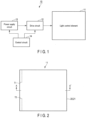
- FIG. 1 is a block diagram of a light control device 10 according to the first embodiment of the present invention.
- the light control device 10 includes a light control element 11, a drive circuit 12, a power supply circuit 13 and a control circuit 14.
- the light control element 11 is an element capable of controlling the light transmittance.
- the light control element 11 is made of, for example, a light control film.
- the light control film is a functional film capable of switching between transparency and opacity (white turbidity). For example, by applying a voltage (maximum voltage) to the light control film, the light control film can be set in a transparent state. On the other hand, by applying 0V (minimum voltage) to the light control film, the light control film is in a white turbidity state. Further, by applying an intermediate voltage between the maximum voltage and the minimum voltage to the light control film, gradation display can be performed stepwise between the transparency and the white turbidity. A specific configuration of the light control element 11 will be described later.
- the drive circuit 12 applies a voltage (drive voltage) to the light control element 11 to drive the light control element 11.
- a circuit configuration of the drive circuit 12 will be described later.
- the power supply circuit 13 receives a power (external power) from the outside.
- the external power is a commercial power, an AC voltage (AC power source), or a DC voltage (DC power source).
- the power supply circuit 13 generates voltages of a plurality of levels necessary for the operation of the light control element 11, using the external power.
- the voltage generated by the power supply circuit 13 is supplied to the drive circuit 12.
- the control circuit 14 controls the drive circuit 12 and the power supply circuit 13.
- the control circuit 14 supplies control signals to the drive circuit 12 and the power supply circuit 13, so that the drive circuit 12 and the power supply circuit 13 can perform desired operations.
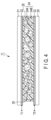
- FIG. 2 is a plan view of the light control element 11.
- FIG. 3 is a cross sectional view taken along line A-A' of FIG. 2 .
- the light control element 11 can take a given planar shape, for example, a square. Where the light control element 11 is a light control film, the light control film is processed in accordance with the outline of a region to be attached.
- the light control element 11 includes base members 20 and 21 disposed opposite to each other, and a liquid crystal layer (light control layer) 24 disposed between the base members 20 and 21.
- the base members 20 and 21 are made of a transparent member, for example, a transparent film.
- a polyethylene terephthalate (PET) film, a polyethylene (PE) film, or a polycarbonate (PC) film can be used as the base members 20 and 21.
- the liquid crystal layer 24 includes a liquid crystal material 24A and a polymer material 24B.
- the liquid crystal layer 24 is made of a polymer dispersed liquid crystal (PDLC) or a polymer network liquid crystal (PNLC).
- the polymer dispersed liquid crystal is composed of a complex in which a liquid crystal material is dispersed in a matrix made of a polymer material; that is, the polymer dispersed liquid crystal has a configuration in which the liquid crystal is phase-separated in the matrix.
- the polymer network liquid crystal is composed of a complex in which a liquid crystal material having a continuous phase is filled in a three-dimensional network structure (polymer network) made of a polymer material.
- a photocurable resin can be used as the polymer material.
- a solution in which a liquid crystal material is mixed with a photopolymerization type polymer precursor (monomer) is irradiated with ultraviolet light to polymerize the monomer, thereby forming a polymer, and the liquid crystal is dispersed in the matrix made of the aforementioned polymer.
- Transparent electrode 22 is provided on base member 20 so as to be in contact with the liquid crystal layer 24.
- Transparent electrode 23 is provided on base member 21 so as to be in contact with the liquid crystal layer 24.
- the transparent electrodes 22 and 23 are made of a material having both light transparency and conductivity, and are made of, for example, ITO (indium tin oxide).
- the light control element 11 includes a terminal T1 electrically connected to transparent electrode 23 and a terminal T2 electrically connected to transparent electrode 22.
- the terminals T1 and T2 are arranged together, for example, on one side of the light control element 11.
- the terminals T1 and T2 are electrically connected to the drive circuit 12.
- the terminals T1 and T2 are made of metal (for example, gold, silver, copper or aluminum).
- the liquid crystal layer 24 is sealed between the transparent electrodes 22 and 23 by a seal member 25.
- the seal member 25 is formed in such a manner as to surround the liquid crystal layer 24.
- the seal member 25 is made of, for example, a photocurable resin.
- the seal member 25 is not necessarily required.
- the seal member 25 is not necessarily required.
- liquid crystal layer (light control layer) 24 Next, a broad operation of the liquid crystal layer (light control layer) 24 will be described.
- the ordinary light refractive index of the liquid crystal material and the refractive index of the polymer material are set to be approximately the same.
- the liquid crystal material for example, a positive (P-type) nematic liquid crystal having positive dielectric anisotropy is used.
- the off state is a state in which the same voltage (for example, 0V) is applied to the transparent electrode 22 and the transparent electrode 23, and no electric field is applied to the liquid crystal layer 24.
- FIG. 3 shows a state of the liquid crystal layer 24 in the off state.
- liquid crystal molecules When no voltage (no electric field) is applied to the liquid crystal layer 24, liquid crystal molecules enter a random state with respect to the interface of the polymer matrix (or the polymer network). In this case, the refractive indexes of the liquid crystal material and the polymer matrix differ, thereby ensuring that incident light is scattered at the interface of the polymer matrix. That is, in a state in which the liquid crystal molecules are not aligned, the liquid crystal layer 24 is in a high haze state. At this time, the liquid crystal layer 24 is in a cloudy state, while the light control element 11 is in an opaque state. In this manner, the light control element 11 can shield an object from an observer.
- the haze value is an index related to the transparency of a member and represents the degree of haze. A smaller haze value indicates a higher transparency.
- the on state is a state in which different voltages (for example, 0V and a positive voltage) are applied to the transparent electrode 22 and the transparent electrode 23, and in which an electric field is applied to the liquid crystal layer 24. Note that an alternating voltage is applied to the transparent electrode 22 and the transparent electrode 23.
- FIG. 4 shows a state of the liquid crystal layer 24 in the on state.
- the major axes (directors) of the liquid crystal molecules align in a direction substantially perpendicular to the electrode planes.
- the refractive indexes of the liquid crystal material and the polymer matrix are substantially the same, so that the incident light is hardly scattered in the liquid crystal layer 24 and passes through the liquid crystal layer 24. That is, in a state in which the liquid crystal molecules are aligned, the liquid crystal layer 24 is in a low haze state. At this time, the light control element 11 is in a transparent state. Therefore, the observer can observe an object through the light control element 11.
- This embodiment describes the case in which the light control element enters an opaque state when no voltage is applied and enters a transparent state when a voltage is applied.
- the present invention is not limited to this case.
- the present invention is also applicable to the case where the light control element 11 is a reverse type that enters a transparent state when no voltage is applied and that enters an opaque state when a voltage is applied.
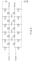
- FIG. 5 is an equivalent circuit diagram of the light control element 11.
- the transparent electrode 22 is formed in a planar shape. Therefore, the transparent electrode 22 constitutes a plurality of resistance components R1 to R11 so as to extend from a terminal side (a side on which the terminals T1 and T2 are arranged) to a distal side (a side opposite to the terminals T1 and T2).
- the transparent electrode 23 is formed in a planar shape. Therefore, the transparent electrode 23 constitutes a plurality of resistance components R12 to R22 so as to extend from the terminal side to the distal side.
- the liquid crystal layer 24 constitutes a plurality of capacitance components C1 to C4 connected between transparent electrode 22 and transparent electrode 23.
- the voltage of the light control element 11 decreases from the terminal side to the terminal side, due to the voltage drop in the resistance components. That is, in the light control element 11, the voltage on the terminal side is high and the voltage on the distal side is low.
- the nodes on the distal side are denoted as N1 and N2.
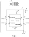
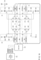
- FIG. 6 is a circuit diagram mainly showing the drive circuit 12.
- the control circuit 14 generates a signal OVPOSIN, a signal CONPOSIN, a signal OVNEGIN and a signal CONNEGIN, and sends these control signals to the drive circuit 12.
- the voltage waveforms of the signal OVPOSIN, signal CONPOSIN, signal OVNEGIN and signal CONNEGIN will be described later.
- the power supply circuit 13 includes a positive side voltage source 30 for overdrive, a negative side voltage source 31 for overdrive, a voltage source 32 that generates a positive side control voltage for controlling the alignment of liquid crystal, and a voltage source 33 for generating a negative side control voltage.
- Voltage source 30 generates overdrive voltage Vov+.
- Voltage source 31 generates overdrive voltage Vov-.
- Voltage source 32 generates control voltage Vc+.
- Voltage source 33 generates control voltage Vc-.
- Positive side control voltage Vc+ and negative side control voltage Vc- are voltages for controlling the alignment of the final liquid crystal, and are determined in accordance with the liquid crystal material used. That is, the voltage at which the liquid crystal molecules are vertically aligned (the threshold voltage of the liquid crystal) is determined in accordance with the liquid crystal material, and the voltage "(Vc+) - (Vc-)" is set equal to or slightly higher than the threshold voltage of the liquid crystal.
- the drive circuit 12 includes switching elements 40-47.
- a first terminal of switching element 40 is connected to voltage source 30, a second terminal thereof is connected to terminal T1, and signal OVPOSIN is input to the control terminal.
- a first terminal of switching element 41 is connected to voltage source 31, a second terminal thereof is connected to terminal T1, and signal OVNEGIN is input to the control terminal.
- Switching element 41 is turned on when the signal OVNEGIN is at the high level, and is turned off when the signal OVNEGIN is at the low level.
- a first terminal of switching element 42 is connected to voltage source 30, a second terminal thereof is connected to terminal T2, and signal OVNEGIN is input to the control terminal.
- Switching element 42 is turned on when the signal OVNEGIN is at the high level, and is turned off when the signal OVNEGIN is at the low level.
- a first terminal of switching element 43 is connected to voltage source 31, a second terminal thereof is connected to terminal T2, and signal OVPOSIN is input to the control terminal.
- Switching element 43 is turned on when the signal OVPOSIN is at the high level, and is turned off when the signal OVPOSIN is at the low level.
- a first terminal of switching element 44 is connected to voltage source 33, a second terminal thereof is connected to the terminal T1, and signal CONNEGIN is input to the control terminal.
- Switching element 44 is turned on when the signal CONNEGIN is at the high level, and is turned off when the signal CONNEGIN is at the low level.
- a first terminal of switching element 45 is connected to voltage source 32, a second terminal thereof is connected to terminal T1, and signal CONPOSIN is input to the control terminal.
- Switching element 45 is turned on when the signal CONPOSIN is at the high level, and is turned off when the signal CONPOSIN is at the low level.
- a first terminal of switching element 46 is connected to voltage source 33, a second terminal thereof is connected to terminal T2, and signal CONPOSIN is input to the control terminal.
- Switching element 46 is turned on when the signal CONPOSIN is at the high level, and is turned off when the signal CONPOSIN is at the low level.
- a first terminal of switching element 47 is connected to voltage source 32, a second terminal thereof is connected to terminal T2, and signal CONNEGIN is input to the control terminal.
- Switching element 47 is turned on when the signal CONNEGIN is at the high level, and is turned off when the signal CONNEGIN is at the low level.
- FIG. 7 is a timing chart for explaining the operation of the control circuit 14. As described above, the control circuit 14 generates the signal OVPOSIN, signal CONPOSIN, signal OVNEGIN and signal CONNEGIN.
- the control circuit 14 sets signal OVPOSIN to the low level (for example, 0V) and sets signal CONPOSIN to the high level.
- control circuit 14 sets signal CONPOSIN to the low level and sets signal OVNEGIN to the high level.
- control circuit 14 sets signal OVNEGIN to the low level and sets signal CONNEGIN to the high level.
- control circuit 14 sets signal CONNEGIN to the low level and sets signal OVPOSIN to the high level. Times t0 to t4 define one cycle, and the same cycle is repeated thereafter.
- FIG. 8 is a timing chart for explaining the operation of the drive circuit 12. Times t0 to t9 in FIG. 8 correspond to times t0 to t9 shown in FIG.7 .
- (1) drive voltage OUT1 which the drive circuit applies to terminal T1 of the light control element 11, (2) drive voltage OUT2 which the drive circuit 12 applies to terminal T2 of the light control element 11, (3) voltage V1out of the node N1 of the light control element 11 and (4) voltage V2out of the node N2 of the light control element 11 are shown.
- FIG. 8 (1) drive voltage OUT1 which the drive circuit applies to terminal T1 of the light control element 11, (2) drive voltage OUT2 which the drive circuit 12 applies to terminal T2 of the light control element 11, (3) voltage V1out of the node N1 of the light control element 11 and (4) voltage V2out of the node N2 of the light control element 11 are shown.
- drive voltage OUT1 is indicated by a solid line
- drive voltage OUT2 is indicated by a broken line
- voltage V1out is indicated by a one-dot chain line
- voltage V2out is indicated by a two-dot chain line.
- switching element 40 In the period t0 to t1, switching element 40 is turned on, and voltage OUT1 is set to Vov+. In the period t0 to t1, switching element 43 is turned on, and voltage OUT2 is set to Vov-.
- voltage V1out on the distal side rises faster than when control voltage Vc+ is applied to terminal T1. Further, voltage V2out on the distal side falls faster than when control voltage Vc- is applied to terminal T2.
- switching element 45 In the period t1 to t2, switching element 45 is turned on, and voltage OUT1 is set to Vc+. In the period t1 to t2, switching element 46 is turned on, and voltage OUT2 is set to Vc-. As a result, voltage V1out on the distal side is set to control voltage Vc+, and voltage V2out on the distal side is set to control voltage Vc-.
- the driving frequency is, for example, 20 Hz.
- the overdrive periods that is, the period t0 to t1 and the period t2 to t3, are set in accordance with the load (resistance and capacitance) of the light control element 11. That is, the overdrive period is set shorter than the period during which voltage V1out on the distal side rises from control voltage Vc- to control voltage Vc+. In addition, the overdrive period is set shorter than the period during which voltage V2out on the distal side falls from control voltage Vc+ to control voltage Vc-.
- FIG. 9 is a graph showing an example of voltagetransmittance (V-T) characteristics of the light control element 11.
- the horizontal axis represents a voltage (V) while the vertical axis represents a transmittance (%), and both axes adopt arbitrary units.
- the voltage shown in FIG. 9 is a voltage applied to the liquid crystal layer 24, that is, a voltage applied between electrodes 22 and 23.
- the transmittance of the light control element 11 can be altered by changing the voltage (drive voltage) applied to the light control element 11. Even if a drive voltage equal to or higher than the saturation voltage is applied to the light control element 11, the transmittance does not change.
- the saturation voltage is a minimum voltage of the voltages that achieve the maximum transmittance. For example, the voltage "(Vc+) - (Vc-)" is set to be below the saturation voltage. Therefore, even if the overdrive voltage is set to a voltage equal to or higher than the saturation voltage within a range that does not exceed the withstand voltage of the liquid crystal, the light control element 11 can be driven using the overdrive voltage, without affecting the transmittance of the liquid crystal.
- the effective voltages on the terminal side are substantially control voltages Vc+ and Vc-. Further, since the voltages on the distal side reach control voltages Vc+ and Vc- at a faster timing, the effective voltages on the distal side are also close to control voltages Vc+ and Vc-. As a result, the difference in the transmittance between the terminal side and the distal side is reduced, and the color unevenness can be reduced.
- the effective voltage applied to the liquid crystal is low, so that the transmittance of the liquid crystal is not a desired transmittance.
- the voltage applied to the liquid crystal is 0V.
- overdriving is used, so that the voltage on the distal side rises at a faster timing. Accordingly, the polarity inversion period can be shortened, and the flicker can be reduced.
- FIG. 10 is a circuit diagram of a drive circuit according to the comparative example.
- Voltage source 32 generates control voltage Vc+.
- Voltage source 33 generates control voltage Vc-.
- a first terminal of switching element 44 is connected to voltage source 33, a second terminal thereof is connected to terminal T1, and signal NEGIN is input to the control terminal.
- Switching element 44 is turned on when the signal NEGIN is at the high level, and is turned off when the signal NEGIN is at the low level.
- a first terminal of switching element 45 is connected to voltage source 32, a second terminal thereof is connected to terminal T1, and signal POSIN is input to the control terminal.
- Switching element 45 is turned on when the signal POSIN is at the high level, and is turned off when the signal POSIN is at the low level.
- a first terminal of switching element 46 is connected to voltage source 33, a second terminal thereof is connected to terminal T2, and signal POSIN is input to the control terminal.
- Switching element 46 is turned on when the signal POSIN is at the high level, and is turned off when the signal POSIN is at the low level.
- a first terminal of switching element 47 is connected to voltage source 32, a second terminal thereof is connected to terminal T2, and signal NEGIN is input to the control terminal.
- Switching element 47 is turned on when the signal NEGIN is at the high level, and is turned off when the signal NEGIN is at the low level.
- FIG. 11 is a diagram for explaining the operation of the light control device according to the comparative example.
- signal POSIN is set to the high level
- signal NEGIN is set to the low level.
- signal POSIN is set to the low level
- signal NEGIN is set to the high level.
- signal POSIN is set to the high level
- signal NEGIN is set to the low level.
- switching element 45 In the period t0 to t1, switching element 45 is turned on, and voltage OUT1 is set to Vc+. In the period t0 to t1, switching element 46 is turned on, and voltage OUT2 is set to Vc-. As a result, voltage V1out on the distal side rises more slowly than in the overdrive driving. Further, voltage V2out on the distal side falls more slowly than in the overdrive driving.
- the light control device 10 includes: base members 20 and 21 disposed to face each other; transparent electrodes 22 and 23 provided on the base members 20 and 21, respectively; a liquid crystal layer 24 filled between the transparent electrodes 22 and 23; a light control element that includes terminals T1 and T2 electrically connected to the transparent electrodes 22 and 23; and a drive circuit 12 that applies drive voltage OUT1 to terminal T1 and that applies drive voltage OUT2 having a polarity different from that of voltage OUT1 to terminal T2.
- Drive voltage OUT1 is set to positive side overdrive voltage Vov+ in the first period, is set to positive side control voltage Vc+ in the second period following the first period, is set to negative side overdrive voltage Vov- in the third period following the second period, and is set to negative side control voltage Vc- in the fourth period following the third period.
- the voltage on the opposite side of the terminal side can be set to the control voltages Vc+ and Vc- more quickly.
- the transmittance difference between the terminal side and the distal side is reduced, and the color unevenness can be reduced.
- Flicker may occur during the polarity inversion period including the zero cross point (the point where voltage V1out and voltage V2out intersect). In this embodiment, however, the polarity inversion period can be shortened, so that the flicker can be reduced.
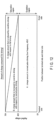
- FIG. 12 is a schematic diagram of the amount of charge consumed according to a first example.
- the horizontal axis represents a position between the terminal and the distal end
- the vertical axis represents the voltage applied to the liquid crystal (applied voltage).
- the region of 0V to 40V is a gradation region in which the transmittance can be changed
- the region of 40V to 70V is a saturation region in which the transmittance does not substantially change.
- Charge amount A is a charge amount in the normal pulse driving.
- the normal pulse driving of the first example is an example in which the applied voltage is 40V and the frequency is lowered until the voltage on the distal side reaches 40V. In the normal pulse driving, the voltage on the distal side finally becomes 40V, so that color unevenness between the terminal side and the distal side can be reduced. However, since the time required for polarity inversion becomes longer, the flicker increases.
- Charge amount B is a charge amount that is increased by the overdrive driving with respect to the normal pulse driving.
- the overdrive driving is an example in which driving is performed using an overdrive voltage of 70V. Since the voltage decreases from the terminal side to the distal side, the charge amount B is represented by a triangle that gradually decreases from the terminal side toward the distal side. Where the overdrive driving is performed, the flicker can be reduced and the color unevenness can be reduced as compared with the case where the normal pulse driving is performed, with only the charge amount B increased.
- Charge amount C is a charge amount that is reduced by the overdrive driving with respect to the full driving.
- the full driving is an example in which driving is performed using 70V. That is, "charge amount A + charge amount B + charge amount C" is a charge amount of the full driving.
- the flicker is reduced, but the amount of charge consumed increases.
- the flicker can be reduced to the same extent as in the full driving, and the amount of charge consumed can be reduced as compared to the full driving.
- FIG. 13 is a schematic diagram of the amount of charge consumed according to a second example.
- the second example is an example in which halftone is executed.
- Charge amount D is a charge amount in the normal pulse driving.
- the normal pulse driving of the second example is an example in which the applied voltage is 20V and the frequency is lowered until the voltage on the distal side reaches 20V. In the normal pulse driving, the voltage on the distal side finally becomes 20V, so that color unevenness between the terminal side and the distal side can be reduced. However, since the time required for polarity inversion becomes longer, the flicker increases. If the frequency is increased in order to reduce the flicker, the potential difference between the terminal side and the distal side increases, and color unevenness occurs. The amount of charge consumed when the frequency is increased is represented by a region that is lower than the broken line in FIG. 13 . As can be seen, the color unevenness and the flicker have a trade-off relationship.
- Charge amount E is a charge amount that is increased by the overdrive driving with respect to the normal pulse driving. Even when halftone is executed using overdrive driving, the flicker can be reduced and the color unevenness can be reduced as compared with the case where the normal pulse driving is performed with only the charge amount E increased. In the second example as well, the overdrive driving can reduce the flicker to the same extent as full driving of 70V.
- the second embodiment is a specific configuration example of the drive circuit 12 and the power supply circuit 13.
- the second embodiment is an example in which the drive circuit 12 is configured in a digital manner using transistors.
- FIG. 14 is a circuit diagram mainly showing a drive circuit 12 according to the second embodiment of the present invention.
- each of the switching elements constituting the drive circuit 12 is configured by a MOS transistor or a bipolar transistor.
- MOS transistor or a bipolar transistor.
- the light control element 11 includes a resistive load RL and a capacitive load CL, as can be understood from FIG. 5 .
- the control circuit 14 includes a timing generation circuit 14A.
- the timing generation circuit 14A controls the timing of signal OVPOSIN, signal CONPOSIN, signal OVNEGIN and signal CONNEGIN.
- the drive circuit 12 includes a gate driver 12A.
- the gate driver 12A receives the signal OVPOSIN, signal CONPOSIN, signal OVNEGIN and signal CONNEGIN from the timing generation circuit 14A.
- the gate driver 12A uses the signal OVPOSIN, signal CONPOSIN, signal OVNEGIN and signal CONNEGIN to set the levels of these signal to gate voltage levels optimum for transistors.
- the gate driver 12A generates a signal OVPOSIN-G, a signal CONPOSIN-G, a signal OVNEGIN-G and a signal CONNEGIN-G.
- the drive circuit 12 includes N-channel MOS transistors 40 to 43, 44A, 44B, 45A, 45B, 46A, 46B, 47A and 47B.
- Signal lines 40S, 42S, 44S, 45S, 46S and 47S are connected to the gate driver 12A.
- the signal lines 40S, 42S, 44S, 45S, 46S and 47S provide the gate driver 12A with the source voltage levels of transistors in order to set the optimal gate voltage levels.
- the drain of transistor 40 is connected to voltage source 30 that generates overdrive voltage Vov+, the source thereof is connected to terminal T1, and the gate thereof is supplied with signal OVPOSIN-G.
- the source of transistor 40 is connected to the gate driver 12A through signal line 40S.
- the drain of transistor 41 is connected to terminal T1, the source thereof is connected to voltage source 31 that generates overdrive voltage Vov-, and the gate thereof is supplied with signal OVNEGIN-G.
- the drain of transistor 42 is connected to voltage source 30, the source thereof is connected to terminal T2, and the gate thereof is supplied with signal OVNEGIN-G.
- the source of transistor 42 is connected to the gate driver 12A through signal line 42S.
- the drain of transistor 43 is connected to terminal T2, the source thereof is connected to voltage source 31, and the gate thereof is supplied with signal OVPOSIN-G.
- Transistors 44A and 44B constitute switching element 44 shown in FIG. 6 .
- the drain of transistor 44A is connected to terminal T1, the source thereof is connected to the source of transistor 44B, and the gate thereof is supplied with signal CONNEGIN-G.
- the drain of transistor 44B is connected to voltage source 33 that generates control voltage Vc-, and the gate thereof is supplied with signal CONNEGIN-G.
- the source of transistor 44A is connected to the gate driver 12A through signal line 44S.
- Transistors 45A and 45B constitute switching element 45 shown in FIG. 6 .
- the drain of transistor 45A is connected to terminal T1, the source thereof is connected to the source of transistor 45B, and the gate thereof is supplied with signal CONPOSIN-G.
- the drain of transistor 45B is connected to voltage source 32 that generates control voltage Vc+, and the gate thereof is supplied with signal CONPOSIN-G.
- the source of transistor 45A is connected to the gate driver 12A through signal line 45S.
- Transistors 46A and 46B constitute switching element 46 shown in FIG. 6 .
- the drain of transistor 46A is connected to terminal T2, the source thereof is connected to the source of transistor 46B, and the gate thereof is supplied with signal CONPOSIN-G.
- the drain of transistor 46B is connected to the voltage source 33, and the gate thereof is supplied with signal CONPOSIN-G.
- the source of transistor 46A is connected to the gate driver 12A through signal line 46S.
- Transistors 47A and 47B constitute switching element 47 shown in FIG. 6 .
- the drain of transistor 47A is connected to terminal T2, the source thereof is connected to the source of transistor 47B, and the gate thereof is supplied with signal CONNEGIN-G.
- the drain of transistor 47B is connected to voltage source 32, and the gate thereof is supplied with signal CONNEGIN-G.
- the source of transistor 47A is connected to the gate driver 12A through signal line 47S.
- the power supply circuit 13 includes a voltage source 13A and voltage sources 30 to 33. Voltage source 13A generates voltage Vin from the power supply voltage VCC.
- Voltage source 30 includes a Zener diode (constant voltage diode) 30A as a constant voltage element, and also includes a resistor (resistive element) 30B.
- the cathode of the Zener diode 30A is connected to voltage source 13A, and the anode thereof is connected to one end of the resistor 30B.
- the other end of the resistor 30B is connected to the ground terminal GND.
- Voltage source 30 may adopt other configurations. For example, where a voltage to be used is high, two or more Zener diodes may be connected in series. Alternatively, an NPN transistor for current amplification may be added to a connection node between the Zener diode 30A and the resistor 30B.
- voltage source 30 may be configured by a series regulator having a voltage control terminal. Further, voltage source 30 may be constituted by a DC/DC converter.
- Voltage source 32 includes a Zener diode 32A and a resistor 32B. One end of the resistor 32B is connected to voltage source 13A, and the other end thereof is connected to the cathode of Zener diode 32A. The anode of Zener diode 32A is connected to a ground terminal GND. Voltage source 32 may use another configuration similar to the configuration of voltage source 30.
- Voltage source 33 includes a Zener diode 33A and a resistor 33B.
- the cathode of Zener diode 33A is connected to voltage source 13A, and the anode thereof is connected to one end of the resistor 33B.
- the other end of the resistor 33B is connected to the ground terminal GND.
- Voltage source 33 may use another configuration similar to the configuration of voltage source 30.
- the drive circuit 12 can be configured using transistors.
- the voltage control in the second embodiment is similar to that performed in the first embodiment.
- the other advantages are similar to the advantages of the first embodiment.
- the third embodiment is a specific configuration example of the drive circuit 12 and the power supply circuit 13.
- the third embodiment is an example in which the drive circuit 12 is configured in an analog manner using power amplifiers.
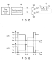
- FIG. 15 is a circuit diagram mainly showing a drive circuit 12 according to the third embodiment of the present invention.
- the drive circuit 12 includes an overdrive waveform generation circuit 12B and power amplifiers 12C and 12D.
- the overdrive waveform generation circuit 12B generates a positive voltage waveform VP and a negative voltage waveform VN, using control signals from the timing generation circuit 14A.
- Power amplifiers 12C and 12D can perform four-quadrant output capable of performing first quadrant to fourth quadrant operations. That is, power amplifiers 12C and 12D can perform current supply (source) and current absorption (sink) regardless of the direction of the voltage.
- Power amplifier 12C receives a positive voltage waveform VP from the overdrive waveform generation circuit 12B and amplifies this positive voltage waveform VP. Power amplifier 12C outputs drive voltage OUT1. The drive voltage OUT1 is applied to terminal T1 of the light control element 11.
- Power amplifier 12D receives a negative voltage waveform VN from the overdrive waveform generation circuit 12B and amplifies this negative voltage waveform VN. Power amplifier 12D outputs drive voltage OUT2. The drive voltage OUT2 is applied to terminal T2 of the light control element 11.
- FIG. 16 is a timing chart for explaining the operation of the drive circuit 12.
- Drive voltages OUT1 and OUT2 have similar waveforms to those shown in FIG. 8 in connection with the first embodiment.
- Drive voltage OUT1 has a similar waveform to that of the positive voltage waveform VP in the previous stage, except that the output current is amplified.
- Drive voltage OUT2 has a similar waveform to that of the negative voltage waveform VN in the previous stage, except that the output current is amplified.
- overdrive driving can be realized in an analog manner.
- the other advantages are similar to the advantages of the first embodiment.
- liquid crystal element using PDLC or PNLC
- the liquid crystal element used as a light control element may have a configuration in which polarizing plates and alignment films are disposed on both sides of a liquid crystal layer, and may employ a TN (Twisted Nematic) method, a VA (Vertical Alignment) method, etc.
- TN Transmission Nematic
- VA Very Alignment
- the switching elements described in connection with the above embodiments may be formed of a SiC-MOSFET using silicon carbide (SiC) for a semiconductor layer, a GaN-MOSFET using gallium nitride (GaN) for a semiconductor layer, etc.
- the light control device described in the above embodiments is applicable to windows and indoor partitions in homes, offices or public facilities, image projection screens and signage in commercial facilities or event venues, windows and sunroofs in automobiles or aircrafts, etc.
- the light control element has been described as an example of the liquid crystal element.
- the driving method described in connection with the above embodiments is applicable to various devices (including a liquid crystal display device) using a liquid crystal.
Landscapes
- Physics & Mathematics (AREA)
- Nonlinear Science (AREA)
- Chemical & Material Sciences (AREA)
- Crystallography & Structural Chemistry (AREA)
- General Physics & Mathematics (AREA)
- Optics & Photonics (AREA)
- Mathematical Physics (AREA)
- Dispersion Chemistry (AREA)
- Liquid Crystal (AREA)
- Control Of Indicators Other Than Cathode Ray Tubes (AREA)
Claims (8)
- Lichtsteuergerät (10), miteinem Lichtsteuerelement (10) einschließlich ersten und zweiten Basiselementen (20, 21), ersten und zweiten Elektroden (22, 23), die jeweilig an den ersten und zweiten Basiselementen vorgesehen sind, einer Flüssigkristallschicht (24), die zwischen den ersten und zweiten Elektroden eingefüllt ist, und ersten und zweiten Anschlüssen (T1, T2), die elektrisch mit den ersten und zweiten Elektroden verbunden sind, undeinem Ansteuerschaltkreis (12), der dazu eingerichtet ist, um eine erste Ansteuerspannung (OUT1) an den ersten Anschluss und eine zweite Ansteuerspannung (OUT2) mit einer Polarität verschieden von jener der ersten Ansteuerspannung an den zweiten Anschluss (T2) anzulegen,wobei der Ansteuerschaltkreis (12) dazu eingerichtet ist, um die erste Ansteuerspannung (OUT1) auf eine erste Spannung (Vov+) in einer ersten Periode, auf eine zweite Spannung (Vc+) geringer als die erste Spannung in einer zweiten Periode folgend auf die erste Periode, auf eine dritte Spannung (Vov-) geringer als die zweite Spannung in einer dritten Periode folgend auf die zweite Periode, und auf eine vierte Spannung (Vc-) geringer als die zweite Spannung und höher als die dritte Spannung in einer vierten Periode folgend auf die dritte Periode einzustellen, undder Ansteuerschaltkreis (12) dazu eingerichtet ist, um die zweite Ansteuerspannung (OUT2) auf die dritte Spannung (Vov-) in der ersten Periode, auf die vierte Spannung (Vc-) in der zweiten Periode, auf die erste Spannung (Vov+) in der dritten Periode, und auf die zweite Spannung (Vc+) in der vierten Periode einzustellen.
- Lichtsteuergerät (10) nach Anspruch 1, wobei eine Spannungsdifferenz zwischen der ersten Spannung (Vov+) und der dritten Spannung (Vov-) kleiner als eine Spannungsfestigkeit des Lichtsteuerelements (11) ist.
- Lichtsteuergerät (10) nach Anspruch 1, wobei eine Spannungsdifferenz zwischen der zweiten Spannung (Vc+) und der vierten Spannung (Vc-) gleich wie oder kleiner als eine Sättigungsspannung des Lichtsteuerelements (11) ist.
- Lichtsteuergerät (10) nach Anspruch 1, wobei der Ansteuerschaltkreis (12) erste bis achte Schaltelemente (40 bis 47) aufweist,das erste Schaltelement (40) zwischen einer ersten Spannungsquelle (30), die die erste Spannung (Vov+) erzeugt, und dem ersten Anschluss (T1) verbunden ist,das zweite Schaltelement (41) zwischen einer dritten Spannungsquelle (31), die die dritte Spannung (Vov-) erzeugt, und dem ersten Anschluss (T1) verbunden ist,das dritte Schaltelement (42) zwischen der ersten Spannungsquelle (30) und dem zweiten Anschluss (T2) verbunden ist,das vierte Schaltelement (43) zwischen der dritten Spannungsquelle (31) und dem zweiten Anschluss (T2) verbunden ist,das fünfte Schaltelement (45) zwischen einer zweiten Spannungsquelle (32), die die zweite Spannung (Vc+) erzeugt, und dem ersten Anschluss (T1) verbunden ist,das sechste Schaltelement (44) zwischen einer vierten Spannungsquelle (33), die die vierte Spannung (Vc-) erzeugt, und dem ersten Anschluss (T1) verbunden ist,das siebte Schaltelement (47) zwischen der zweiten Spannungsquelle (32) und dem zweiten Anschluss (T2) verbunden ist, unddas achte Schaltelement (46) zwischen der vierten Spannungsquelle (33) und dem zweiten Anschluss (T2) verbunden ist.
- Lichtsteuergerät (10) nach Anspruch 4, ferner mit:einem Steuerschaltkreis (14), der erste bis vierte Steuersignale (OVPOSIN, OVNEGIN, CONPOSIN, CONNEGIN) erzeugt,wobei das erste Steuersignal (OVPOSIN) zu den ersten und vierten Schaltelementen (40, 43) eingegeben ist,das zweite Steuersignal (OVNEGIN) zu den zweiten und dritten Schaltelementen (41, 42) eingegeben ist,das dritte Steuersignal (CONPOSIN) zu den fünften und achten Schaltelementen (45, 46) eingegeben ist, unddas vierte Steuersignal (CONNEGIN) zu den sechsten und siebten Schaltelementen (44, 47) eingegeben ist.
- Lichtsteuergerät (10) nach Anspruch 5, wobeidas erste Steuersignal (OVPOSIN) in der ersten Periode aktiviert ist,das dritte Steuersignal (CONPOSIN) in der zweiten Periode aktiviert ist,das zweite Steuersignal (OVNEGIN) in der dritten Periode aktiviert ist, unddas vierte Steuersignal (CONNEGIN) in der vierten Periode aktiviert ist.
- Lichtsteuergerät (10) nach Anspruch 4, wobei jede der ersten bis vierten Spannungsquellen (30 bis 33) ein Konstantspannungselement (30A, 32A, 33A) aufweist.
- Lichtsteuergerät (10) nach Anspruch 4, wobei jedes der ersten bis achten Schaltelemente (40 bis 47) einen Transistor umfasst.
Applications Claiming Priority (2)
| Application Number | Priority Date | Filing Date | Title |
|---|---|---|---|
| JP2017113443A JP6981052B2 (ja) | 2017-06-08 | 2017-06-08 | 調光装置 |
| PCT/JP2018/021054 WO2018225625A1 (ja) | 2017-06-08 | 2018-05-31 | 調光装置 |
Publications (3)
| Publication Number | Publication Date |
|---|---|
| EP3637176A1 EP3637176A1 (de) | 2020-04-15 |
| EP3637176A4 EP3637176A4 (de) | 2020-06-10 |
| EP3637176B1 true EP3637176B1 (de) | 2024-04-24 |
Family
ID=64565864
Family Applications (1)
| Application Number | Title | Priority Date | Filing Date |
|---|---|---|---|
| EP18812822.7A Active EP3637176B1 (de) | 2017-06-08 | 2018-05-31 | Lichtsteuervorrichtung |
Country Status (5)
| Country | Link |
|---|---|
| US (1) | US10871668B2 (de) |
| EP (1) | EP3637176B1 (de) |
| JP (1) | JP6981052B2 (de) |
| CN (1) | CN110678805B (de) |
| WO (1) | WO2018225625A1 (de) |
Families Citing this family (3)
| Publication number | Priority date | Publication date | Assignee | Title |
|---|---|---|---|---|
| KR102018352B1 (ko) * | 2019-02-25 | 2019-10-21 | 주식회사 제이앤에스 | Haze 특성이 개선된 스마트 필름 장치 |
| JP7263938B2 (ja) * | 2019-06-20 | 2023-04-25 | 凸版印刷株式会社 | 調光シート駆動装置、調光装置、調光シートの駆動方法、および、調光シートの駆動プログラム |
| BR112023026207A2 (pt) * | 2021-06-23 | 2024-03-05 | Japan Display Inc | Dispositivo óptico |
Citations (1)
| Publication number | Priority date | Publication date | Assignee | Title |
|---|---|---|---|---|
| WO2006030388A2 (en) * | 2004-09-15 | 2006-03-23 | Koninklijke Philips Electronics N.V. | Display devices and methods of driving such |
Family Cites Families (14)
| Publication number | Priority date | Publication date | Assignee | Title |
|---|---|---|---|---|
| JPS6449924A (en) | 1987-08-20 | 1989-02-27 | Teraoka Seiko Kk | Strain gage type load cell |
| JPS6449924U (de) * | 1987-09-24 | 1989-03-28 | ||
| JPH10197849A (ja) * | 1997-01-06 | 1998-07-31 | Matsushita Electric Ind Co Ltd | 反強誘電性液晶素子の駆動方法および駆動装置 |
| TWI259992B (en) * | 2003-05-22 | 2006-08-11 | Au Optronics Corp | Liquid crystal display device driver and method thereof |
| JP2005010202A (ja) * | 2003-06-16 | 2005-01-13 | Nec Corp | 液晶パネル、該液晶パネルを用いた液晶表示装置および該液晶表示装置を搭載した電子機器 |
| TWI329214B (en) * | 2003-12-18 | 2010-08-21 | Sharp Kk | Display element and display device, driving method of display element, and program |
| TWI282544B (en) * | 2005-01-21 | 2007-06-11 | Himax Tech Inc | Operation apparatus, operation method, operation apparatus for overdrive and operation method for overdrive |
| JP4661406B2 (ja) * | 2005-07-05 | 2011-03-30 | 富士ゼロックス株式会社 | 液晶デバイスの駆動方法、および液晶デバイス駆動装置 |
| JP2007304561A (ja) * | 2006-03-23 | 2007-11-22 | Toshiba Matsushita Display Technology Co Ltd | 液晶表示装置の駆動装置 |
| JP4645632B2 (ja) * | 2007-09-21 | 2011-03-09 | ソニー株式会社 | 液晶表示装置、液晶表示装置の駆動方法および電子機器 |
| WO2009063661A1 (ja) * | 2007-11-13 | 2009-05-22 | Sharp Kabushiki Kaisha | 電源回路およびそれを備える表示装置 |
| JP2013072895A (ja) * | 2011-09-26 | 2013-04-22 | Seiko Electric Co Ltd | 液晶調光装置及び液晶調光素子の駆動装置 |
| TWM494455U (zh) * | 2014-09-23 | 2015-01-21 | Unity Opto Technology Co Ltd | 改善led頻閃之驅動電路 |
| WO2018178043A1 (en) * | 2017-03-29 | 2018-10-04 | Merck Patent Gmbh | Method for electrically driving a switchable optical element |
-
2017
- 2017-06-08 JP JP2017113443A patent/JP6981052B2/ja active Active
-
2018
- 2018-05-31 CN CN201880035752.8A patent/CN110678805B/zh active Active
- 2018-05-31 EP EP18812822.7A patent/EP3637176B1/de active Active
- 2018-05-31 WO PCT/JP2018/021054 patent/WO2018225625A1/ja unknown
-
2019
- 2019-12-05 US US16/704,526 patent/US10871668B2/en active Active
Patent Citations (1)
| Publication number | Priority date | Publication date | Assignee | Title |
|---|---|---|---|---|
| WO2006030388A2 (en) * | 2004-09-15 | 2006-03-23 | Koninklijke Philips Electronics N.V. | Display devices and methods of driving such |
Also Published As
| Publication number | Publication date |
|---|---|
| CN110678805A (zh) | 2020-01-10 |
| CN110678805B (zh) | 2022-08-23 |
| US10871668B2 (en) | 2020-12-22 |
| JP2018205631A (ja) | 2018-12-27 |
| WO2018225625A1 (ja) | 2018-12-13 |
| EP3637176A1 (de) | 2020-04-15 |
| US20200110297A1 (en) | 2020-04-09 |
| JP6981052B2 (ja) | 2021-12-15 |
| EP3637176A4 (de) | 2020-06-10 |
Similar Documents
| Publication | Publication Date | Title |
|---|---|---|
| US10871668B2 (en) | Light control device | |
| KR20120110387A (ko) | 화소 회로 및 화소 회로의 구동 방법 | |
| US10890791B2 (en) | Light control device | |
| US20100033475A1 (en) | Liquid crystal display and control method thereof | |
| US8633921B2 (en) | Data driving circuit and liquid crystal display device including the same | |
| CN109410880B (zh) | 显示面板驱动电路 | |
| CN113056702A (zh) | 相位调制装置以及相位调制方法 | |
| US9741301B2 (en) | Driving circuit of display panel, display device, and method for driving the driving circuit of the display panel | |
| KR20100006320A (ko) | 백라이트 유닛의 광원 구동장치 및 방법 | |
| CN102930841A (zh) | 近晶态液晶多稳态电子纸显示器的像素电路 | |
| CN101963728A (zh) | 液晶显示器 | |
| CN104834132A (zh) | 显示面板、调试画面闪烁的方法及装置、显示装置 | |
| US10971106B2 (en) | Liquid crystal optical modulation device and liquid crystal optical modulation method | |
| CN106548738B (zh) | 显示系统中电源供应模块及相关驱动装置及电源供应方法 | |
| US7999778B2 (en) | Apparatus and method for driving LCD | |
| CN101290756B (zh) | 伽玛电压的产生装置、液晶显示装置及控制伽玛电压的方法 | |
| KR20080043508A (ko) | 액정표시장치 및 그의 구동 방법 | |
| JP7226510B2 (ja) | 調光装置 | |
| KR20100034242A (ko) | Lcd 드라이버 | |
| KR20000006515A (ko) | 액정표시소자의구동방법 | |
| KR100200369B1 (ko) | 액정 표시 장치용 플리커 제어 회로 | |
| JP2011085801A (ja) | Tft液晶駆動回路、及びそれを用いたtft液晶駆動方法 | |
| US20050219191A1 (en) | System for driving columns of a liquid crystal display | |
| JP2007212689A (ja) | 液晶表示素子 | |
| WO2010095313A1 (ja) | 表示装置および表示装置の駆動方法 |
Legal Events
| Date | Code | Title | Description |
|---|---|---|---|
| STAA | Information on the status of an ep patent application or granted ep patent |
Free format text: STATUS: THE INTERNATIONAL PUBLICATION HAS BEEN MADE |
|
| PUAI | Public reference made under article 153(3) epc to a published international application that has entered the european phase |
Free format text: ORIGINAL CODE: 0009012 |
|
| STAA | Information on the status of an ep patent application or granted ep patent |
Free format text: STATUS: REQUEST FOR EXAMINATION WAS MADE |
|
| 17P | Request for examination filed |
Effective date: 20191219 |
|
| AK | Designated contracting states |
Kind code of ref document: A1 Designated state(s): AL AT BE BG CH CY CZ DE DK EE ES FI FR GB GR HR HU IE IS IT LI LT LU LV MC MK MT NL NO PL PT RO RS SE SI SK SM TR |
|
| AX | Request for extension of the european patent |
Extension state: BA ME |
|
| A4 | Supplementary search report drawn up and despatched |
Effective date: 20200511 |
|
| RIC1 | Information provided on ipc code assigned before grant |
Ipc: G02F 1/13 20060101ALI20200504BHEP Ipc: G02F 1/133 20060101AFI20200504BHEP |
|
| DAV | Request for validation of the european patent (deleted) | ||
| DAX | Request for extension of the european patent (deleted) | ||
| STAA | Information on the status of an ep patent application or granted ep patent |
Free format text: STATUS: EXAMINATION IS IN PROGRESS |
|
| 17Q | First examination report despatched |
Effective date: 20220117 |
|
| GRAP | Despatch of communication of intention to grant a patent |
Free format text: ORIGINAL CODE: EPIDOSNIGR1 |
|
| STAA | Information on the status of an ep patent application or granted ep patent |
Free format text: STATUS: GRANT OF PATENT IS INTENDED |
|
| INTG | Intention to grant announced |
Effective date: 20231219 |
|
| GRAS | Grant fee paid |
Free format text: ORIGINAL CODE: EPIDOSNIGR3 |
|
| GRAA | (expected) grant |
Free format text: ORIGINAL CODE: 0009210 |
|
| STAA | Information on the status of an ep patent application or granted ep patent |
Free format text: STATUS: THE PATENT HAS BEEN GRANTED |
|
| AK | Designated contracting states |
Kind code of ref document: B1 Designated state(s): AL AT BE BG CH CY CZ DE DK EE ES FI FR GB GR HR HU IE IS IT LI LT LU LV MC MK MT NL NO PL PT RO RS SE SI SK SM TR |
|
| REG | Reference to a national code |
Ref country code: GB Ref legal event code: FG4D |
|
| REG | Reference to a national code |
Ref country code: CH Ref legal event code: EP |
|
| REG | Reference to a national code |
Ref country code: DE Ref legal event code: R096 Ref document number: 602018068627 Country of ref document: DE |
|
| REG | Reference to a national code |
Ref country code: IE Ref legal event code: FG4D |