EP3588570B1 - Procédé de fabrication d'un module d'affichage - Google Patents
Procédé de fabrication d'un module d'affichage Download PDFInfo
- Publication number
- EP3588570B1 EP3588570B1 EP19182141.2A EP19182141A EP3588570B1 EP 3588570 B1 EP3588570 B1 EP 3588570B1 EP 19182141 A EP19182141 A EP 19182141A EP 3588570 B1 EP3588570 B1 EP 3588570B1
- Authority
- EP
- European Patent Office
- Prior art keywords
- layer
- area
- base layer
- hole
- bending
- Prior art date
- Legal status (The legal status is an assumption and is not a legal conclusion. Google has not performed a legal analysis and makes no representation as to the accuracy of the status listed.)
- Active
Links
Images


Classifications
-
- H—ELECTRICITY
- H10—SEMICONDUCTOR DEVICES; ELECTRIC SOLID-STATE DEVICES NOT OTHERWISE PROVIDED FOR
- H10W—GENERIC PACKAGES, INTERCONNECTIONS, CONNECTORS OR OTHER CONSTRUCTIONAL DETAILS OF DEVICES COVERED BY CLASS H10
- H10W72/00—Interconnections or connectors in packages
- H10W72/01—Manufacture or treatment
- H10W72/019—Manufacture or treatment of bond pads
-
- G—PHYSICS
- G02—OPTICS
- G02F—OPTICAL DEVICES OR ARRANGEMENTS FOR THE CONTROL OF LIGHT BY MODIFICATION OF THE OPTICAL PROPERTIES OF THE MEDIA OF THE ELEMENTS INVOLVED THEREIN; NON-LINEAR OPTICS; FREQUENCY-CHANGING OF LIGHT; OPTICAL LOGIC ELEMENTS; OPTICAL ANALOGUE/DIGITAL CONVERTERS
- G02F1/00—Devices or arrangements for the control of the intensity, colour, phase, polarisation or direction of light arriving from an independent light source, e.g. switching, gating or modulating; Non-linear optics
- G02F1/01—Devices or arrangements for the control of the intensity, colour, phase, polarisation or direction of light arriving from an independent light source, e.g. switching, gating or modulating; Non-linear optics for the control of the intensity, phase, polarisation or colour
- G02F1/13—Devices or arrangements for the control of the intensity, colour, phase, polarisation or direction of light arriving from an independent light source, e.g. switching, gating or modulating; Non-linear optics for the control of the intensity, phase, polarisation or colour based on liquid crystals, e.g. single liquid crystal display cells
- G02F1/133—Constructional arrangements; Operation of liquid crystal cells; Circuit arrangements
- G02F1/1333—Constructional arrangements; Manufacturing methods
- G02F1/1345—Conductors connecting electrodes to cell terminals
- G02F1/13452—Conductors connecting driver circuitry and terminals of panels
-
- G—PHYSICS
- G02—OPTICS
- G02F—OPTICAL DEVICES OR ARRANGEMENTS FOR THE CONTROL OF LIGHT BY MODIFICATION OF THE OPTICAL PROPERTIES OF THE MEDIA OF THE ELEMENTS INVOLVED THEREIN; NON-LINEAR OPTICS; FREQUENCY-CHANGING OF LIGHT; OPTICAL LOGIC ELEMENTS; OPTICAL ANALOGUE/DIGITAL CONVERTERS
- G02F1/00—Devices or arrangements for the control of the intensity, colour, phase, polarisation or direction of light arriving from an independent light source, e.g. switching, gating or modulating; Non-linear optics
- G02F1/01—Devices or arrangements for the control of the intensity, colour, phase, polarisation or direction of light arriving from an independent light source, e.g. switching, gating or modulating; Non-linear optics for the control of the intensity, phase, polarisation or colour
- G02F1/13—Devices or arrangements for the control of the intensity, colour, phase, polarisation or direction of light arriving from an independent light source, e.g. switching, gating or modulating; Non-linear optics for the control of the intensity, phase, polarisation or colour based on liquid crystals, e.g. single liquid crystal display cells
- G02F1/133—Constructional arrangements; Operation of liquid crystal cells; Circuit arrangements
- G02F1/1333—Constructional arrangements; Manufacturing methods
- G02F1/1345—Conductors connecting electrodes to cell terminals
- G02F1/13454—Drivers integrated on the active matrix substrate
-
- G—PHYSICS
- G02—OPTICS
- G02F—OPTICAL DEVICES OR ARRANGEMENTS FOR THE CONTROL OF LIGHT BY MODIFICATION OF THE OPTICAL PROPERTIES OF THE MEDIA OF THE ELEMENTS INVOLVED THEREIN; NON-LINEAR OPTICS; FREQUENCY-CHANGING OF LIGHT; OPTICAL LOGIC ELEMENTS; OPTICAL ANALOGUE/DIGITAL CONVERTERS
- G02F1/00—Devices or arrangements for the control of the intensity, colour, phase, polarisation or direction of light arriving from an independent light source, e.g. switching, gating or modulating; Non-linear optics
- G02F1/01—Devices or arrangements for the control of the intensity, colour, phase, polarisation or direction of light arriving from an independent light source, e.g. switching, gating or modulating; Non-linear optics for the control of the intensity, phase, polarisation or colour
- G02F1/13—Devices or arrangements for the control of the intensity, colour, phase, polarisation or direction of light arriving from an independent light source, e.g. switching, gating or modulating; Non-linear optics for the control of the intensity, phase, polarisation or colour based on liquid crystals, e.g. single liquid crystal display cells
- G02F1/133—Constructional arrangements; Operation of liquid crystal cells; Circuit arrangements
- G02F1/1333—Constructional arrangements; Manufacturing methods
- G02F1/1345—Conductors connecting electrodes to cell terminals
- G02F1/13458—Terminal pads
-
- H—ELECTRICITY
- H10—SEMICONDUCTOR DEVICES; ELECTRIC SOLID-STATE DEVICES NOT OTHERWISE PROVIDED FOR
- H10D—INORGANIC ELECTRIC SEMICONDUCTOR DEVICES
- H10D86/00—Integrated devices formed in or on insulating or conducting substrates, e.g. formed in silicon-on-insulator [SOI] substrates or on stainless steel or glass substrates
- H10D86/01—Manufacture or treatment
- H10D86/021—Manufacture or treatment of multiple TFTs
-
- H—ELECTRICITY
- H10—SEMICONDUCTOR DEVICES; ELECTRIC SOLID-STATE DEVICES NOT OTHERWISE PROVIDED FOR
- H10D—INORGANIC ELECTRIC SEMICONDUCTOR DEVICES
- H10D86/00—Integrated devices formed in or on insulating or conducting substrates, e.g. formed in silicon-on-insulator [SOI] substrates or on stainless steel or glass substrates
- H10D86/40—Integrated devices formed in or on insulating or conducting substrates, e.g. formed in silicon-on-insulator [SOI] substrates or on stainless steel or glass substrates characterised by multiple TFTs
- H10D86/441—Interconnections, e.g. scanning lines
-
- H—ELECTRICITY
- H10—SEMICONDUCTOR DEVICES; ELECTRIC SOLID-STATE DEVICES NOT OTHERWISE PROVIDED FOR
- H10D—INORGANIC ELECTRIC SEMICONDUCTOR DEVICES
- H10D86/00—Integrated devices formed in or on insulating or conducting substrates, e.g. formed in silicon-on-insulator [SOI] substrates or on stainless steel or glass substrates
- H10D86/40—Integrated devices formed in or on insulating or conducting substrates, e.g. formed in silicon-on-insulator [SOI] substrates or on stainless steel or glass substrates characterised by multiple TFTs
- H10D86/60—Integrated devices formed in or on insulating or conducting substrates, e.g. formed in silicon-on-insulator [SOI] substrates or on stainless steel or glass substrates characterised by multiple TFTs wherein the TFTs are in active matrices
-
- H—ELECTRICITY
- H10—SEMICONDUCTOR DEVICES; ELECTRIC SOLID-STATE DEVICES NOT OTHERWISE PROVIDED FOR
- H10K—ORGANIC ELECTRIC SOLID-STATE DEVICES
- H10K59/00—Integrated devices, or assemblies of multiple devices, comprising at least one organic light-emitting element covered by group H10K50/00
- H10K59/10—OLED displays
- H10K59/12—Active-matrix OLED [AMOLED] displays
- H10K59/131—Interconnections, e.g. wiring lines or terminals
-
- H—ELECTRICITY
- H10—SEMICONDUCTOR DEVICES; ELECTRIC SOLID-STATE DEVICES NOT OTHERWISE PROVIDED FOR
- H10K—ORGANIC ELECTRIC SOLID-STATE DEVICES
- H10K71/00—Manufacture or treatment specially adapted for the organic devices covered by this subclass
- H10K71/10—Deposition of organic active material
- H10K71/12—Deposition of organic active material using liquid deposition, e.g. spin coating
- H10K71/13—Deposition of organic active material using liquid deposition, e.g. spin coating using printing techniques, e.g. ink-jet printing or screen printing
-
- H—ELECTRICITY
- H10—SEMICONDUCTOR DEVICES; ELECTRIC SOLID-STATE DEVICES NOT OTHERWISE PROVIDED FOR
- H10K—ORGANIC ELECTRIC SOLID-STATE DEVICES
- H10K71/00—Manufacture or treatment specially adapted for the organic devices covered by this subclass
- H10K71/60—Forming conductive regions or layers, e.g. electrodes
-
- H—ELECTRICITY
- H10—SEMICONDUCTOR DEVICES; ELECTRIC SOLID-STATE DEVICES NOT OTHERWISE PROVIDED FOR
- H10K—ORGANIC ELECTRIC SOLID-STATE DEVICES
- H10K77/00—Constructional details of devices covered by this subclass and not covered by groups H10K10/80, H10K30/80, H10K50/80 or H10K59/80
- H10K77/10—Substrates, e.g. flexible substrates
- H10K77/111—Flexible substrates
-
- H—ELECTRICITY
- H10—SEMICONDUCTOR DEVICES; ELECTRIC SOLID-STATE DEVICES NOT OTHERWISE PROVIDED FOR
- H10W—GENERIC PACKAGES, INTERCONNECTIONS, CONNECTORS OR OTHER CONSTRUCTIONAL DETAILS OF DEVICES COVERED BY CLASS H10
- H10W20/00—Interconnections in chips, wafers or substrates
- H10W20/20—Interconnections within wafers or substrates, e.g. through-silicon vias [TSV]
-
- H—ELECTRICITY
- H10—SEMICONDUCTOR DEVICES; ELECTRIC SOLID-STATE DEVICES NOT OTHERWISE PROVIDED FOR
- H10W—GENERIC PACKAGES, INTERCONNECTIONS, CONNECTORS OR OTHER CONSTRUCTIONAL DETAILS OF DEVICES COVERED BY CLASS H10
- H10W20/00—Interconnections in chips, wafers or substrates
- H10W20/40—Interconnections external to wafers or substrates, e.g. back-end-of-line [BEOL] metallisations or vias connecting to gate electrodes
-
- H—ELECTRICITY
- H10—SEMICONDUCTOR DEVICES; ELECTRIC SOLID-STATE DEVICES NOT OTHERWISE PROVIDED FOR
- H10W—GENERIC PACKAGES, INTERCONNECTIONS, CONNECTORS OR OTHER CONSTRUCTIONAL DETAILS OF DEVICES COVERED BY CLASS H10
- H10W72/00—Interconnections or connectors in packages
- H10W72/90—Bond pads, in general
-
- H—ELECTRICITY
- H10—SEMICONDUCTOR DEVICES; ELECTRIC SOLID-STATE DEVICES NOT OTHERWISE PROVIDED FOR
- H10K—ORGANIC ELECTRIC SOLID-STATE DEVICES
- H10K77/00—Constructional details of devices covered by this subclass and not covered by groups H10K10/80, H10K30/80, H10K50/80 or H10K59/80
-
- H—ELECTRICITY
- H10—SEMICONDUCTOR DEVICES; ELECTRIC SOLID-STATE DEVICES NOT OTHERWISE PROVIDED FOR
- H10W—GENERIC PACKAGES, INTERCONNECTIONS, CONNECTORS OR OTHER CONSTRUCTIONAL DETAILS OF DEVICES COVERED BY CLASS H10
- H10W70/00—Package substrates; Interposers; Redistribution layers [RDL]
- H10W70/01—Manufacture or treatment
- H10W70/05—Manufacture or treatment of insulating or insulated package substrates, or of interposers, or of redistribution layers
-
- H—ELECTRICITY
- H10—SEMICONDUCTOR DEVICES; ELECTRIC SOLID-STATE DEVICES NOT OTHERWISE PROVIDED FOR
- H10W—GENERIC PACKAGES, INTERCONNECTIONS, CONNECTORS OR OTHER CONSTRUCTIONAL DETAILS OF DEVICES COVERED BY CLASS H10
- H10W70/00—Package substrates; Interposers; Redistribution layers [RDL]
- H10W70/60—Insulating or insulated package substrates; Interposers; Redistribution layers
- H10W70/62—Insulating or insulated package substrates; Interposers; Redistribution layers characterised by their interconnections
- H10W70/65—Shapes or dispositions of interconnections
- H10W70/652—Cross-sectional shapes
-
- H—ELECTRICITY
- H10—SEMICONDUCTOR DEVICES; ELECTRIC SOLID-STATE DEVICES NOT OTHERWISE PROVIDED FOR
- H10W—GENERIC PACKAGES, INTERCONNECTIONS, CONNECTORS OR OTHER CONSTRUCTIONAL DETAILS OF DEVICES COVERED BY CLASS H10
- H10W90/00—Package configurations
-
- Y—GENERAL TAGGING OF NEW TECHNOLOGICAL DEVELOPMENTS; GENERAL TAGGING OF CROSS-SECTIONAL TECHNOLOGIES SPANNING OVER SEVERAL SECTIONS OF THE IPC; TECHNICAL SUBJECTS COVERED BY FORMER USPC CROSS-REFERENCE ART COLLECTIONS [XRACs] AND DIGESTS
- Y02—TECHNOLOGIES OR APPLICATIONS FOR MITIGATION OR ADAPTATION AGAINST CLIMATE CHANGE
- Y02E—REDUCTION OF GREENHOUSE GAS [GHG] EMISSIONS, RELATED TO ENERGY GENERATION, TRANSMISSION OR DISTRIBUTION
- Y02E10/00—Energy generation through renewable energy sources
- Y02E10/50—Photovoltaic [PV] energy
- Y02E10/549—Organic PV cells
-
- Y—GENERAL TAGGING OF NEW TECHNOLOGICAL DEVELOPMENTS; GENERAL TAGGING OF CROSS-SECTIONAL TECHNOLOGIES SPANNING OVER SEVERAL SECTIONS OF THE IPC; TECHNICAL SUBJECTS COVERED BY FORMER USPC CROSS-REFERENCE ART COLLECTIONS [XRACs] AND DIGESTS
- Y02—TECHNOLOGIES OR APPLICATIONS FOR MITIGATION OR ADAPTATION AGAINST CLIMATE CHANGE
- Y02P—CLIMATE CHANGE MITIGATION TECHNOLOGIES IN THE PRODUCTION OR PROCESSING OF GOODS
- Y02P70/00—Climate change mitigation technologies in the production process for final industrial or consumer products
- Y02P70/50—Manufacturing or production processes characterised by the final manufactured product
Definitions
- the present invention is directed to a method of manufacturing a display module with a reduced width of a non-display area.
- US 2014/184057 A1 describes an electronic device with an organic light-emitting diode display with minimized border regions.
- the border regions may be minimized by providing conductive structures that pass through polymer layers of the display and/or conductive structures that wrap around an edge of the display and couple conductive traces on the display to conductive traces on additional circuitry that is mounted behind the display.
- US 2016/336532 A1 describes a slim-bezel flexible display device and a manufacturing method thereof.
- CN 107 039 377 A describes a display panel and a manufacturing method thereof, and a display device. After a chip on film is adhered by adhesive to a side away from the display surface of a display substrate, signal lines around the display surface of the display substrate can be connected with connecting terminals arranged on the chip on film through a conductive material arranged in connecting holes which at least penetrate through the display substrate, the signal lines and an insulating layer.
- US 2018/053905 A1 describes a display apparatus capable of reducing generation of defects such as a disconnection during manufacturing processes, while ensuring longer lifespan thereof.
- a process of electrically connecting the display panel and a drive chip may be performed.
- Such a coupling process may be classified into a process of a chip-on-glass (“COG”) mounting method and a process of a tape-automated-bonding (“TAB”) mounting method according to the driving chip mounting method.
- COG chip-on-glass
- TAB tape-automated-bonding
- the TAB mounting method is a method of bonding a tape carrier package or a flexible film on which a driving chip is mounted to a display panel. This method also uses the ACF to bond the display panel to one end of the tape carrier package or flexible film and to bond the printed circuit board to the other end of the tape carrier package or flexible film.
- An embodiment of the invention provides a method of manufacturing a display as recited in claim 1.
- the method may further include: removing a portion of the bending area; and bending the bending area in a way such that the first contact hole and the second contact hole overlap each other when viewed from a plan view in a thickness direction of the display module, where the forming the conductive part may include providing the conductive material to the first contact hole and the second contact hole.
- the method may further include: providing a first mask layer on the upper surface of the circuit layer; forming a first mask pattern by patterning the first mask layer; forming the first contact hole and the second contact hole using the first mask pattern; removing the portion of the bending area using the first mask pattern; providing a second mask layer on the upper surface of the circuit layer; forming a second mask pattern by patterning the second mask layer; and patterning the circuit layer using the second mask pattern.
- the method may further include: providing a mask layer on the upper surface of the circuit layer; forming a first mask pattern by patterning the mask layer; forming the first contact hole and the second contact hole using the first mask pattern; forming a second mask pattern by ashing a portion of the first mask pattern; and patterning the circuit layer using the second mask pattern.
- the method may further include, after the bending of the bending area, grinding a portion of the bending area.
- the removing the portion of the bending area may include removing the portion of the bending area in a way such that the first pad area and the second pad area are connected to each other by a remaining portion of the bending area.
- the base layer may include a first alignment pattern disposed in the first pad area and a second alignment pattern disposed in the second pad area, and the method may further include bending the bending area in a way such that the second alignment pattern is aligned with the first alignment pattern.
- the base layer may include a first alignment pattern
- the circuit member includes a second alignment pattern
- the method may further include disposing the circuit member on a back surface of the base layer in a way such that the second alignment pattern is aligned with the first alignment pattern.
- the base layer may be provided in plurality, and the forming the base layer may include: providing a preliminary base layer, portions of which define base layers, respectively, on the carrier substrate; and forming a connection portion connecting the base layers to each other by removing a portion of the preliminary base layer, where the forming the connection portion and the forming the through hole may be performed at the same time.
- the sub-base layer and the circuit member may be disposed on a back surface of the base layer, and the display module may further include a connection conductive part connecting the sub-base layer and the circuit member.
- the base layer may include a first alignment pattern
- the sub-base layer may include a second alignment pattern, wherein the first alignment pattern may be aligned with the second alignment pattern when viewed from the plan view in the thickness direction of the display module.
- the base layer may include a first alignment pattern
- the circuit member may include a second alignment pattern, wherein the first alignment pattern may be aligned with the second alignment pattern when viewed from the plan view in the thickness direction of the display module.
- a display device includes at least one display module, where the display module includes: a base layer where a first hole is defined; a wiring layer disposed on the base layer, where a second hole is defined in the wiring layer on an area corresponding to the first hole when viewed from a plan view in a thickness direction of the display module; a sub-base layer disposed below the base layer, where a third hole is defined in the sub-base layer on an area corresponding to the second hole when viewed from the plan view in the thickness direction of the display module; a sub-wiring layer disposed below the sub-base layer, where a fourth hole is defined in the sub-wiring layer on an area corresponding to the third hole when viewed from the plan view in the thickness direction of the display module; a circuit member disposed below the base layer; and a conductive part disposed in the first hole and the second hole to electrically connect the wiring layer and the circuit member.
- Exemplary embodiments are described herein with reference to cross section illustrations that are schematic illustrations of idealized embodiments. As such, variations from the shapes of the illustrations as a result, for example, of manufacturing techniques and/or tolerances, are to be expected. Thus, embodiments described herein should not be construed as limited to the particular shapes of regions as illustrated herein but are to include deviations in shapes that result, for example, from manufacturing. For example, a region illustrated or described as flat may, typically, have rough and/or nonlinear features. Moreover, sharp angles that are illustrated may be rounded. Thus, the regions illustrated in the figures are schematic in nature and their shapes are not intended to illustrate the precise shape of a region and are not intended to limit the scope of the present claims.
- FIG. 1 is a perspective view of a display device according to an embodiment not forming part of the invention.
- an embodiment of a display device DD may display an image through a display area DA.
- the display area DA has a surface defined by a first direction DR1 and a second direction DR2 intersecting the first direction DR1 is shown, but embodiments are not limited thereto.
- the display area DA of the display device DD may have a curved shape.
- the thickness direction of the display device DD is indicated by the third direction DR3.
- the directions that the first to third directions DR1, DR2, and DR3 indicate may be converted to other directions as a relative concept.
- the term "on a plane" means when viewed from a plan view in the third direction DR3.
- the display device DD may be a television.
- the display device DD may be used in medium-sized electronic devices such as personal computers, notebook computers, personal digital terminals, car navigation units, game machines, smart phones, tablets, and cameras in addition to large-sized electronic devices such as monitors, or external billboards, for example, but not being limited thereto.
- the display device DD may be employed in other electronic devices.
- FIG. 2A is a plan view showing display modules constituting a display device according to an embodiment not forming part of the invention.
- the display device DD may include a plurality of display modules DM.
- the display modules DM may be arranged along the first direction DR1 and the second direction DR2, respectively.
- three display modules DM are arranged in the first direction DR1 and three display modules DM are arranged in the second direction DR2.
- a total of nine display modules DM are arranged, but not being limited thereto.
- the number of the display modules DM included in the display device DD may be variously modified depending on the size of the display device DD or the size of the display modules DM.
- each of the display modules DM may have a rectangular shape on a plane, but not being limited thereto.
- the shape of each of the display modules DM may be variously modified.
- Each of the display modules DM may include a display area DA0 and a non-display area NDAO.
- the display area DA0 may be an area where a pixel light emission area PXA is defined and an image is displayed
- the non-display area NDAO may surround the display area DA0 and may not display an image.
- FIG. 2B is a plan view showing a display module constituting a display device according to an embodiment not forming part of the invention.
- an embodiment of the display device DD may include one display module DM1.
- the display module DM1 may include a display area DA1 and a non-display area NDA1.
- the display area DA1 of the display module DM1 may correspond to the display area DA of the display device DD. However, this is merely exemplary, and the display area DA1 may have a larger area than the display area DA.
- the area ratio of the display area DA1 of the display module DM1 to the total area of the display module DM1 may be increased. Therefore, the size of a display screen may be increased by increasing the area ratio of the display area DA1 without increasing the size of a substrate.
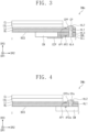
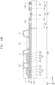
- FIG. 3 is a cross-sectional view taken along line I-I' shown in FIG. 2B showing an embodiment of the display module.
- the display module DMa of FIG. 3 is an embodiment of the display module DM1 of FIG. 2B or the display modules DM of FIG. 2A .
- Each of the display modules DM in FIG. 2A may have a different size from the display module DM1 of FIG. 2B but may have substantially the same structure as the display module DM1 of FIG. 2B .
- Each of the base layer BL and the sub-base layer SBL may include a flexible material, and may be, for example, a plastic substrate.
- the plastic substrate may include at least one selected from acrylic resin, methacrylic resin, polyisoprene, vinyl resin, epoxy resin, urethane resin, cellulose resin, siloxane-based resin, polyimide-based resin, polyamide-based resin, and perylene resin.
- the base layer BL and the sub-base layer SBL may include a single-layer polyimide-based resin.
- the base layer BL may have a multi-layer structure (e.g., laminated structure) including a plurality of insulating layers.
- a first hole HL1 may be defined in the base layer BL.
- the first hole HL1 may be a hole extending from an upper surface of the base layer BL toward a lower surface of the base layer BL.
- a wiring layer LL may be disposed on the upper surface of the base layer BL.
- the wiring layer LL may define a conductive layer constituting a circuit layer.
- a second hole HL2 may be defined in one region of the wiring layer LL.
- the one region may be a region overlapping the first hole HL1 on a plane or when viewed from a thickness direction (i.e., the third direction DR3) of the display panel DMa or the base layer BL.
- the second hole HL2 may be a hole extending from the upper surface of the wiring layer LL toward the lower surface of the wiring layer LL.
- the sub-base layer SBL may be disposed under the base layer BL.
- the sub-base layer SBL may have a same layer structure and include a same material as the base layer BL.
- the sub-base layer SBL may be a layer cut from the base layer BL. In FIG. 3 , the base layer BL and the sub-base layer SBL are hatched in a same manner for convenience of illustration.
- a third hole HL3 may be defined in the sub-base layer SBL.
- the third hole HL3 may be defined on a plane in a region overlapping the first hole HL1 and the second hole HL2.
- the third hole HL3 may be a hole extending from the upper surface of the sub-base layer SBL toward the lower surface of the sub-base layer SBL.
- a sub-wiring layer SLL may be disposed under the sub-base layer SBL.
- the sub-wiring layer SLL may have a same layer structure as the wiring layer LL.
- the sub-wiring layer SLL may be a layer formed by a same process as the wiring layer LL.
- a fourth hole HL4 may be defined in the sub-wiring layer SLL.
- the fourth hole HL4 may be defined in a region overlapping the first through third holes HL1, HL2, and HL3 on a plane.
- the fourth hole HL4 may be a hole extending from the upper surface of the sub-wiring layer SLL toward the lower surface of the sub-wiring layer SLL.
- the first hole HL1, the second hole HL2, the third hole HL3 and the fourth hole HL4 may overlap each other on a plane.
- the upper surface of the uppermost wiring layer LL to the lower surface of the lowest sub-wiring layer SLL may be penetrated by the first hole HL1, the second hole HL2, the third hole HL3 and the fourth hole HL4.
- a through hole is defined by the first hole HL1, the second hole HL2, the third hole HL3, and the fourth hole HL4.
- a conductive part CP may be disposed in the first hole HL1, the second hole HL2, the third hole HL3 and the fourth hole HL4.
- the conductive part CP may be disposed in the first hole HL1, the second hole HL2, the third hole HL3 and the fourth hole HL4 from the upper part of the wiring layer LL.
- a portion CPP of the conductive part CP may be disposed on the upper surface of the wiring layer LL.
- at least a portion of the upper surface of the wiring layer LL may be covered by a portion CPP of the conductive part CP.
- the contact between the wiring layer LL and the conductive part CP may be more stable, and the contact resistance between the wiring layer LL and the conductive part CP may be reduced since the contact area therebetween increases.
- the conductive part CP extends through the first to fourth holes HL1, HL2, HL3 and HL4 to electrically connect a first structure disposed on the upper surface of the base layer BL and a second structure disposed on the lower surface of the base layer BL.
- a connection member for connecting the first structure and the second structure may be omitted, and the area for the connection member to be disposed in the base layer BL may be omitted. Therefore, in such an embodiment, the width of the non-display area NDA1 (see FIG. 2B ) of the display module DMa may be reduced.
- the image display element layer IDL may be disposed over the wiring layer LL.
- the image display element layer IDL may be a layer that operates to display an image.
- the image display element layer IDL may include a light emitting diode ("LED") element, for example a tiny LED element.
- the image display element layer IDL may include organic LEDs, inorganic LEDs, or organic-inorganic hybrid LEDs.
- the image display element layer IDL may include liquid crystal molecules that control light transmission.
- a cover layer CL may be disposed on the image display element layer IDL.
- the cover layer CL may serve to seal the image display element layer IDL.
- the cover layer CL may protect the image display element layer IDL from foreign substances such as moisture/oxygen or dust particles.
- the cover layer CL may have a laminate structure or be a substrate.
- the laminate structure may include at least one organic sealing layer and at least one inorganic sealing layer, which are alternately stacked one on another.
- the substrate may be a glass substrate or a plastic substrate.
- the circuit member CM may be disposed under the base layer BL.
- the circuit member CM may supply a signal for controlling the image display element layer IDL.
- the circuit member CM may be a printed circuit board ("PCB”), a flexible printed circuit board (“FPCB”), a flexible film on which a driving chip is mounted, or a tape carrier package on which a driving chip is mounted.
- the sub-base layer SBL and the circuit member CM may be disposed on the lower surface or a back surface BCS of the base layer BL.
- an adhesive member (not shown) may be disposed between the back surface BCS of the base layer BL and the circuit member CM and between the back surface BCS of the base layer BL and the circuit member CM.
- the adhesive member may be a double-sided tape.
- connection conductive part CCP that connects the sub-wiring layer SLL and the circuit member CM may be disposed below the sub-wiring layer SLL and the circuit member CM.
- the connection conductive part CCP may include a conductive material.
- a conductive material may be printed on each of the sub-wiring layer SLL and the circuit member CM to form the connection conductive part CCP.
- the wiring layer LL may be electrically connected to the circuit member CM by the conductive part CP, the sub-wiring layer SLL and the connection conductive part CCP.
- the conductive material may be, for example, a conductive ink or a conductive paste.
- the conductive ink may be a material in which conductive particles are mixed with ink
- the conductive paste may be a material in which conductive particles are dispersed in a fluid resin solution.
- the conductive particles may be, for example, organometallic complexes, metal powders or inorganic compounds, and may include, for example, copper, carbon, graphene, gold, silicon, platinum or quantum dots.
- the materials of the conductive particles described above are merely exemplary, and the conductive particles are not limited to the above examples.
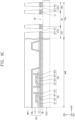
- FIG. 4 is a cross-sectional view taken along line I-I' shown in FIG. 2B showing an alternative embodiment of the display module.
- the same reference numerals are assigned to the same components as those described in FIG. 3 , and any repetitive detailed description thereof will be omitted or simplified.
- the display module DMb of FIG. 4 shows an alternative embodiment of the display module DM1 of FIG. 2B or the display modules DM of FIG. 2A .
- Each of the display modules DM in FIG. 2A may have a different size from the display module DM1 of FIG. 2B but may have substantially the same structure as the display module DM1 of FIG. 2B .
- the display module DMb may include a base layer BL, a wiring layer LL, an image display element layer IDL, a circuit member CM, a cover layer CL, and a conductive part CPa.
- the sub-base layer SBL (see FIG. 3 ) and the sub-wiring layer SLL (see FIG. 3 ) may be omitted in FIG. 4 .
- the conductive part CPa may be disposed in the first hole HL1 and the second hole HL2 from the upper part of the wiring layer LL.
- a through hole is defined by the first hole HL1 and the second hole HL2.
- a portion CPPa of the conductive part CPa may be disposed on the upper surface of the wiring layer LL. Thus, at least a portion of the upper surface of the wiring layer LL may be covered by the portion CPPa of the conductive part CPa.
- the circuit member CM is disposed under the base layer BL and may be disposed in a region overlapping the conductive part CPa on the plane or when viewed from the plan view in the thickness direction of the display module DMb. Therefore, the circuit member CM may be electrically connected to the wiring layer LL through the conductive part CPa.
- the base layer BL may include a first alignment pattern AP1 and the circuit member CM may include a second alignment pattern AP2a.
- the second alignment pattern AP2a may be aligned corresponding to the first alignment pattern AP1.
- the first alignment pattern AP1 may be printed on the base layer BL and the second alignment pattern AP2a may be printed on the circuit member CM.
- the alignment between the base layer BL and the circuit member CM may be performed with improved accuracy by the first alignment pattern AP1 and the second alignment pattern AP2a.
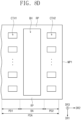
- FIG. 5A is a plan view showing the first alignment pattern shown in FIGS. 3 and 4
- FIG. 5B is a plan view showing the second alignment pattern shown in FIGS. 3 and 4 .
- the first alignment pattern AP1 may have a cross shape.
- the second alignment pattern AP2 may have a shape corresponding to the shape of the first alignment pattern AP1 such that the first alignment pattern AP1 may be aligned with the second alignment pattern AP2.
- the second alignment pattern AP2 may include four rectangular shapes arranged to be disposed around the first alignment pattern AP1, as shown in FIG. 5B .
- the shapes of the first and second alignment patterns AP1 and AP2 described with reference to FIGS. 5A and 5B are merely exemplary, and the shapes of the first and second alignment patterns AP1 and AP2 may be variously modified. In one embodiment, for example, the shapes of the first and second alignment patterns AP1 and AP2 may be reversed, that is, the first and second alignment patterns AP1 and AP2 may have the shapes shown in FIGS. 5B and 5A , respectively.
- the first alignment pattern AP1 may have a circular or polygonal shape
- the second alignment pattern AP2 has a shape corresponding to the shape of the first alignment pattern AP1 as long as the second alignment pattern AP2 has a shape that may be aligned with the circular or polygonal first alignment pattern AP1.
- the second alignment pattern AP2 on the plane may have a shape that does not overlap with the first alignment pattern AP1.
- FIG. 6 is a circuit diagram showing a pixel according to an embodiment not forming part of the invention.
- the pixel PX may be connected to a plurality of signal lines.
- the scan lines SL, the data lines DL, the first power line PL1, and the second power line PL2 are shown in FIG. 6 .
- the pixel PX may include an image display element ED and a pixel circuit PXC.
- the pixel circuit PXC may include a first thin film transistor TR1, a capacitor CAP, and a second thin film transistor TR2.
- the first thin film transistor TR1 may be a switching transistor for controlling ON-OFF of the pixel PX.
- the first thin film transistor TR1 may transmit or block a data signal transmitted through the data line DL in response to a gate signal transmitted through the scan line SL.
- the capacitor CAP is connected to the first thin film transistor TR1 and the first power line PL1.
- the capacitor CAP charges an amount of charge corresponding to the difference between the data signal transferred from the first thin film transistor TR1 and the first power supply voltage ELVDD applied to the first power line PL1.
- the second thin film transistor TR2 is connected to the first thin film transistor TR1, the capacitor CAP and the image display element ED.
- the second thin film transistor TR2 controls the driving current flowing in the image display element ED in correspondence to the amount of charge stored in the capacitor CAP.
- the turn-on time of the second thin film transistor TR2 may be determined by the amount of charge charged in the capacitor CAP.
- the second thin film transistor TR2 provides the first power supply voltage ELVDD transmitted through the first power line PL1 to the image display element ED during the turn-on time.
- the image display element ED is connected to the second thin film transistor TR2 and the second power line PL2.
- the image display element ED emits light at a voltage corresponding to the difference between the signal transmitted through the second thin film transistor TR2 and the second power supply voltage ELVSS received through the second power line PL2.
- the image display element ED includes a light emitting material.
- the image display element ED may generate light of a color corresponding to the light emitting material.
- the color of the light generated in the image display element ED may be any one of red, green, blue, and white.
- each of the first thin film transistor TR1 and the second thin film transistor TR2 may be an N-type thin film transistor or a P-type thin film transistor.
- one of the first thin film transistor TR1 and the second thin film transistor TR2 may be an N-type thin film transistor and the other of the first thin film transistor TR1 and the second thin film transistor TR2 may be a P-type thin film transistor.
- the first semiconductor pattern SP1 and the second semiconductor pattern SP2 may be disposed on the first insulating layer L1.
- the first semiconductor pattern SP1 may be spaced apart from the first control electrode CE1 on the cross section or in a thickness direction of the base layer BL
- the second semiconductor pattern SP2 may be spaced apart from the second control electrode CE2 on the cross section or in a thickness direction of the base layer BL.
- a second insulating layer L2 may be disposed over the first insulating layer L1, and may cover the first and second semiconductor patterns SP1 and SP2, the first and second input electrodes IE1 and IE2, and the first and second output electrodes OE1 and OE2.
- the first and second semiconductor patterns SP1 and SP2, the first and second input electrodes IE1 and IE2, and the first and second output electrodes OE1 and OE2 may be disposed between the first insulating layer L1 and the second insulating layer L2.
- a connection electrode CCE that connects the first output electrode OE1 and the second control electrode CE2 may be disposed on the third insulating layer L3.
- through holes may be defined in the second and third insulating layers L2 and L3, and a portion of the first output electrode OE1 may be exposed through the through holes.
- the connection electrode CCE may be electrically connected to the exposed portion of the first output electrode OE1.
- Through holes are defined through the first to third insulating layers L1, L2 and L3, and a portion of the second control electrode CE2 may be exposed through the through holes.
- the connection electrode CCE may be electrically connected to the exposed portion of the second control electrode CE2.
- a fourth insulating layer L4 may be disposed on the third insulating layer L3.
- the fourth insulating layer L4 may cover a portion of the first electrode E1a and may expose another portion of the first electrode E1a.
- the fourth insulating layer L4 may be a pixel definition layer.
- a pixel light emission area PXA may be defined corresponding to the first electrode E1a exposed by the fourth insulating layer L4.
- the light emission layer EM is disposed on the first electrode E1a.
- the light emission layer EM may include a luminescent material.
- the light emission layer EM may include at least one of materials for emitting red, green or blue light, and may include a fluorescent material or a phosphorescent material.
- the light emission layer EM may emit light in response to a potential difference between the first electrode E1a and the second electrode E2a.
- the second electrode E2a may include a transmissive conductive material or a transflective conductive material, such that the light generated in the light emission layer EM may be effectively emitted through the second electrode E2a.
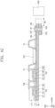
- FIGS. 8A to 8K are cross-sectional views showing a part of a manufacturing process of a display module according to an embodiment of the invention.
- FIGS. 8A to 8K schematically show a manufacturing process of a display module having the pixels described in FIG. 7A .
- a base layer BL is provided, e.g., formed, on a carrier substrate STG1.
- the carrier substrate STG1 may be, for example, a glass substrate.
- a display area DAB and a pad area PDA may be defined in the base layer BL.
- the circuit layer CCL is provided or formed on the display area DAB and the pad area PDA of the base layer BL.
- the circuit layer CCL may include a plurality of conductive layers, a plurality of insulating layers, and a semiconductor layer.
- the plurality of conductive layers may include a first control electrode CE1, a first input electrode IE1, a first output electrode OE1, a second control electrode CE2, a second input electrode IE2, a second output electrode OE2, a wiring layer LL, and a conductive layer CDL.
- the plurality of insulating layers may include first to third insulating layers L1, L2, and L3.
- the semiconductor layer may include a first semiconductor pattern SP1 and a second semiconductor pattern SP2.
- the wiring layer LL may be a layer provided or formed through a same process as the conductive layer CDL and including a same material as the conductive layer CDL. However, the invention is not limited thereto. In one alternative embodiment, for example, the wiring layer LL may be provided or formed through a same process as the first control electrode CE1, and may be a layer including a same material as the first control electrode CE1. In another alternative embodiment of the invention, the wiring layer LL may be provided or formed through a same process as the first input electrode IE1, and may be a layer including a same material as the first input electrode IE1.
- a first mask layer MPL is provided or formed on the upper surface of the circuit layer CCL.
- the first mask layer MPL may be a polymer layer.
- the first mask layer MPL may be a photoresist layer that is exposed to light or heat to change resistance.
- a first mask pattern MP1 is provided or formed by patterning the first mask layer MPL (see FIG. 8A ).
- the first mask layer MPL disposed in the pad area PDA may be removed to form the first mask pattern MP1.
- the first mask pattern MP1 may be a photoresist pattern.
- holes may be formed in the wiring layer LL and the base layer BL using the first mask pattern MP1.
- a wet etching process or a dry etching process may be used to form holes in the wiring layer LL and the base layer BL.
- a first pad area PD1, a bending area BA, and a second pad area PD2 are defined in the pad area PDA.
- a bending area BA is defined between the first pad area PD1 and the second pad area PD2.
- a first contact hole CTH1 may be formed in the first pad area PD1
- a second contact hole CTH2 may be formed in the second pad area PD2
- at least a portion of the bending area BA may be removed.
- the first contact hole CTH1 is defined by the first hole HL1 and the second hole HL2 and the second contact hole CTH2 is defined by the third hole HL3 and the fourth hole HL4.
- the first hole HL1 and the second hole HL2 may overlap each other and the third hole HL3 and the fourth hole HL4 may overlap each other.
- a bending hole BH may be defined in the bending area BA.
- FIG. 8D a plan view of a first mask pattern MP1 disposed in a pad area PDA is shown.
- the first contact holes CTH1, the second contact holes CTH2, and the bending holes BH formed by the first mask pattern MP1 are also illustrated.
- the bending hole BH may be an area corresponding to a portion removed from the bending area BA. There may be portions not removed in the peripheral portion of the bending hole BH of the bending area BA. The portion not removed around the bending hole BH is referred to as a remaining portion RP.
- the first pad area PD1 and the second pad area PD2 may be connected to each other by the remaining portion RP.
- the first mask pattern MP1 is removed.
- a second mask layer (not shown) is formed on the circuit layer CCL.
- the second mask layer may be in a substantially same form as the first mask layer MPL shown in FIG. 8A .
- the second mask layer may be a polymer layer.
- the second mask layer may be a photoresist layer that is exposed to light or heat to change resistance.
- the second mask layer is patterned to form a second mask pattern MP2.
- a portion of the second mask layer disposed in the display area DAB and the pad area PDA may be removed to form the second mask pattern MP2.
- the second mask pattern MP2 may be a photoresist pattern.
- connection electrode CCE, the first electrode E1 and the second electrode E2 may be formed by patterning the conductive layer CDL (see FIG. 8C ).
- a wet etching process may be used to form the connection electrode CCE, the first electrode E1 and the second electrode E2.
- a dry etching process may be used to from the connection electrode CCE, the first electrode E1 and the second electrode E2.
- the wiring lines LNS and pads PDS may be formed by patterning the wiring layer LL (see FIG. 8C ).
- the patterned wiring layer LL may include wiring lines LNS and pads PDS.
- FIG. 8F a plan view of a second mask pattern MP2 disposed in a pad area PDA is shown.
- the second mask pattern MP2 When viewed from the plan view in the thickness direction of the display module, the second mask pattern MP2 may have a shape corresponding to the shape of the wiring lines LNS and the pads PDS of the wiring layer LL (see FIG. 8C ). For better understanding, reference numerals of wiring lines LNS and pads PDS formed by the second mask pattern MP2 are also illustrated.
- FIGS. 8G , 8H , 8I , and 8J a portion not disposed on a same cross-sectional plane is shown by a dotted line.
- the dotted line shown in the bending area BA may be the remaining portion RP described above with reference to FIG. 8D .
- the micro-sized LED element ED1 is transferred to the first electrode E1 and the second electrode E2.
- a plurality of micro-sized LED elements ED1 may be transferred simultaneously, or a single micro-sized LED element ED1 may be transferred.
- the method of transferring the micro-sized LED element ED1 to the first electrode E1 and the second electrode E2 may include a direct transfer method or a print transfer method.
- the direct transfer method may be a method of transferring the micro-sized LED element ED1 directly to the first electrode E1 and the second electrode E2.
- the print transfer method may be a method of transferring the micro-sized LED element ED1 to the first electrode E1 and the second electrode E2 using an electrostatic head, a flat stamp, or a roll stamp.
- the base layer BL is moved to the bending jig STG2.
- a protective film (not shown) for protecting the circuit layer CCL may be further provided on the circuit layer CCL.
- the bending area BA of the base layer BL may be bent in a way such that the first contact hole CTH1 and the second contact hole CTH2 overlap.
- the second pad area PD2 disposed under the first pad area PD1 may defined a sub-base layer SBL (see FIG. 3 ) and the wiring layer LL disposed on the base layer BL of the second pad area PD2 may define a sub-wiring layer SLL(see FIG. 3 ).
- a conductive material CI is provided, e.g., injected, in the first and second contact holes CTH1 and CTH2 and then the conductive material CI is cured to form a conductive part CP.
- the curing may be a thermal curing, a dry curing, or a ultraviolet ("UV”) curing, but not being limited thereto.
- the conductive part CP may electrically connect the wiring lines LNS and the pads PDS corresponding one-to-one to the wiring lines LNS. Being disposed in the first contact hole CTH1 may mean filling the empty space defined by the first contact hole CTH1.
- a target to be connected e.g., the wiring lines LNS and the pads PDS
- a conductive part CP is formed.
- the contact area may be more stable because the contact area between the wiring lines LNS and the conductive part CP increases.
- the contact resistance between the wiring lines LNS and the conductive part CP may be reduced.
- a portion of the pads PDS may have a shape covered by a portion of the conductive part CP.
- the bending area BA may be ground by a grinder GRD.
- GRD grinder
- FIGS. 9A to 9C are cross-sectional views showing a part of a manufacturing process of a display module according to an alternative embodiment of the invention.
- the first mask pattern MP1a (see FIG. 9A ) is ashed to form a second mask pattern MP2a.
- the second mask pattern MP2a in the pad area PDA may correspond to the second mask pattern MP2 shown in FIG. 8F .
- a wiring layer LL (see FIG. 9B ) and a conductive layer CDL (see FIG. 9B ) are patterned using a second mask pattern MP2a.
- the connection electrode CCE, the first electrode E1, and the second electrode E2 may be formed by patterning the conductive layer CDL, and the wiring layer LL may be patterned to form wiring lines LNS and pads PDS.
- the wiring layer LL may include wiring lines LNS and pads PDS.
- a first contact hole CTH1 is formed in a first pad area PD1 and a second contact hole CTH2 is formed in a second pad area PD2 by using a first mask pattern MP1b. Thereafter, the first mask pattern MP1b is ashed, and the wiring layer LL and the conductive layer CDL are patterned using the ashed mask pattern.
- the connection electrode CCE, the first electrode E1, and the second electrode E2 may be formed by patterning the conductive layer CDL.
- a part of the wiring layer LL of the bending area BA and a part of the base layer BLa of the bending area BA may also be removed.
- the first thickness TN1 of at least a portion in the bending area BA of the base layer BLa may be less than the second thickness TN2 of the base layer BLa of each of the first pad area PD1 and the second pad area PD2.
- the first thickness TN1 (see FIG. 10B ) in the bending area BA is less than the second thickness TN2 (see FIG. 10B ) of the base layer BLa of each of the first pad area PD1 and the second pad area PD2, bending of the bending area BA may become easier.
- FIGS. 11A to 11C are cross-sectional views showing a part of a manufacturing process of a display module according to another alternative embodiment of the invention.
- a first mask pattern MP1c is formed by patterning a first mask layer MPL.
- at least a portion of the first mask layer MPL disposed in the pad area PDA may be removed to form the first mask pattern MP1c, and at least a portion of the first mask layer MPL disposed in the first pad area PD1 and the second pad area PD2 may be removed.
- a first contact hole CTH1 is formed in a first pad area PD1 and a second contact hole CTH2 is formed in a second pad area PD2 by using a first mask pattern MP1c. After the first contact holes CTH1 and the second contact holes CTH2 are formed, the first mask pattern MP1c is removed.
- a second mask layer (not shown) is provided or formed on the circuit layer CCL.
- the second mask layer may be provided in a substantially same form as the first mask layer MPL shown in FIG. 8A .
- the bending area BA of the base layer BL is half-cut.
- the base layer BL may be half-cut by a laser LS or may be half-cut by a knife.
- the half-cutting means not cutting the entire thickness of the base layer BL but cutting a part of the thickness of the base layer BL.
- the bending of the base layer BL may become easier.
- FIG. 12 is a cross-sectional view showing a part of a manufacturing process of a display module according to another alternative embodiment of the invention.
- the upper surface of the base layer BL may be half-cut, but in an alternative embodiment, as shown in FIG. 12 , the lower surface of the base layer BL may be half-cut.
- FIGS. 13A to 13D are cross-sectional views showing a part of a manufacturing process of a display module according to an embodiment of the invention.
- FIG. 13E is a plan view of a base layer according to an embodiment of the invention.
- FIG. 13F is a cross-sectional view taken along line II-II' shown in FIG. 13E .
- a preliminary base layer BBL is provided or formed on a carrier substrate STG.
- the preliminary base layer BBL may include a material for securing flexibility.
- the preliminary base layer BBL may include a same material as the base layer BL (see FIG. 3 ) described above with reference to FIG. 3 .
- the circuit layer CCL may include a plurality of conductive layers, a plurality of insulating layers, and a semiconductor layer.
- a through hole CTH and a boundary hole BCTH are formed in the preliminary base layer BBL and the circuit layer CCL by using a photoresist pattern PR.
- the through hole CTH and the boundary hole BCTH may be formed at the same time, e.g., simultaneously during a same process.
- the through hole CTH may include the first hole HL1 and the second hole HL2 described with reference to FIG. 4 . At least a part of the preliminary base layer BBL may be removed to form the boundary hole BCTH and the base layers BLS1, BLS2 and BLS3 may be separated by the boundary hole BCTH. Further, as the boundary hole BCTH is formed, the connection portions CBL (see FIG. 13D ) may be formed.
- two base layers BLS1 and BLS2 may be spaced apart from each other with the boundary hole BCTH therebetween.
- Each of the base layers BLS1, BLS2, and BLS3 may constitute one display module.
- the boundary hole BCTH may be defined on a plane between two base layers BLS1 and BLS2 and between two connection portions CBL.
- FIG. 13C an embodiment having a structure in which a boundary hole BCTH is formed between two base layers BLS1 and BLS2 and between two connection portions CBL are disposed is shown, but the invention is not limited thereto.
- the boundary hole BCTH may be provided in plurality, and a connection portion CBL may be additionally disposed between the plurality of boundary holes BCTH.
- the area for handling during the display module fabrication process may also be reduced as the width of a non-display area is reduced.
- Connection portions CBL may be provided to secure an area for the handling.
- connection portions CBL may be removed in a later process.
- the connection portions CBL may be removed by a chamfering process.
- the connection portions CBL may be removed by a laser or removed by a knife.
- the base layer BLS1 may include first sides SD1 extending in the first direction DR1 and second sides SD2 extending in the second direction DR2, and a connection side CD for connecting one of the first sides SD1 and one of the second sides SD2.
- the connection portions CBL are provided in a portion adjacent to four vertices
- the number of connection sides CD may be four.
- FIG. 13E shows an embodiment where the connection side CD has a straight line shape, but the invention is not limited thereto.
- the connection side CD may have a curved shape on a plane.
- FIG. 13F is a cross-sectional view taken along line II-II' shown in FIG. 13E .
- a circuit member CM may be disposed directly below the base layer BL, and the circuit member CM may be electrically connected to the circuit layer CCL through a conductive part CP disposed in the through hole CTH. Thus, the width of the non-display area may be reduced.
- a hole is defined in the base layer of the display panel, and a wiring layer disposed on one side of the base layer and a circuit member disposed on the other side of the base layer may be electrically connected by a conductive part disposed in the hole. Therefore, the width of the non-display area of the display panel may be reduced.
- a portion of the conductive part may cover a portion of the wiring layer.
- the contact resistance may be reduced, and also, as the contact area increases, the contact between the wiring layer and the conductive part may be more stable.
Landscapes
- Physics & Mathematics (AREA)
- Nonlinear Science (AREA)
- Mathematical Physics (AREA)
- Chemical & Material Sciences (AREA)
- Crystallography & Structural Chemistry (AREA)
- General Physics & Mathematics (AREA)
- Optics & Photonics (AREA)
- Engineering & Computer Science (AREA)
- Microelectronics & Electronic Packaging (AREA)
- Manufacturing & Machinery (AREA)
- Devices For Indicating Variable Information By Combining Individual Elements (AREA)
- Electroluminescent Light Sources (AREA)
Claims (9)
- Procédé de fabrication d'un module d'affichage (DM),
le procédé comprenant les étapes de :fourniture d'un substrat porteur (STG1) ;fourniture d'une couche de base (BL), où une zone d'affichage (DAB) et une zone de plot (PDA) sont définies, sur le substrat porteur (STG1) ;fourniture d'une couche de circuit (CCL) sur la zone d'affichage (DAB) de la couche de base (BL) et la zone de plot (PDA) de la couche de base (BL) ;formation d'un trou traversant dans la couche de circuit (CCL) et la couche de base (BL) sur la zone de plot (PDA) ;formation d'une partie conductrice (CP) en fournissant un matériau conducteur à partir d'une surface supérieure de la couche de circuit (CCL) jusqu'au trou traversant formé dans la zone de plot (PDA) ; etfourniture d'un organe de circuit (CM) connecté électriquement à la couche de circuit (CCL) sous la couche de base (BL)caractérisé en ce quela zone de plot de la couche de base (BL) définit une première zone de plot (PD1), une zone de flexion (BA) et une deuxième zone de plot (PD2),la zone de flexion (BA) est positionnée entre la première zone de plot (PD1) et la deuxième zone de plot (PD2),la formation du trou traversant comprend :la formation d'un premier trou de contact (CTH1) dans la couche de circuit (CCL) sur la première zone de plot (PD1) et dans la première zone de plot (PD1) de la couche de base (BL) ; etla formation d'un deuxième trou de contact (CTH2) dans la couche de circuit sur la deuxième zone de plot (PD2) et dans la deuxième zone de plot (PD2) de la couche de base (BL). - Procédé selon la revendication 1, comprenant en outre :l'enlèvement d'une portion de la zone de flexion (BA) ; etla flexion de la zone de flexion (BA) de manière à ce que le premier trou de contact (CTH1) et le deuxième trou de contact (CTH2) se chevauchent lorsqu'ils sont vus à partir d'une vue en plan dans une direction d'épaisseur du module d'affichage (DM),dans lequel la formation de la partie conductrice (CP) comprend la fourniture du matériau conducteur au premier trou de contact (CTH1) et au deuxième trou de contact (CTH2).
- Procédé selon la revendication 2, comprenant en outre :la fourniture d'une première couche de masque (MPL) sur la surface supérieure de la couche de circuit (CCL) ;la formation d'un premier motif de masque (MP1) par formation de motif sur la première couche de masque (MPL) ;la formation du premier trou de contact (HL1) et du deuxième trou de contact (HL2) à l'aide du premier motif de masque (MP1) ;l'enlèvement de la portion de la zone de flexion (BA) à l'aide du premier motif de masque (MP1) ;la fourniture d'une deuxième couche de masque sur la surface supérieure de la couche de circuit (CCL) ; etla formation d'un deuxième motif de masque (MP2) par formation de motif sur la deuxième couche de masque ;la formation de motif sur la couche de circuit (CCL) à l'aide du deuxième motif de masque (MP2).
- Procédé selon au moins l'une des revendications 1 et 2, comprenant en outre :la fourniture d'une couche de masque sur la surface supérieure de la couche de circuit (CCL) ;la formation d'un premier motif de masque (MP1) par formation de motif sur la couche de masque ;la formation du premier trou de contact (CTH1) et du deuxième trou de contact (CTH2) à l'aide du premier motif de masque (MP1) ;la formation d'un deuxième motif de masque (MP2) par calcination d'une portion du premier motif de masque (MP1) ; etla formation de motif sur la couche de circuit (CCL) à l'aide du deuxième motif de masque (MP2).
- Procédé selon au moins l'une des revendications 2 à 4, lorsqu'elle dépend de la revendication 2, comprenant en outre :
après la flexion de la zone de flexion (BA), le meulage de la portion de la zone de flexion (BA). - Procédé selon au moins l'une des revendications 2 à 5, lorsqu'elle dépend de la revendication 2, dans lequel l'enlèvement de la portion de la zone de flexion (BA) comprend l'enlèvement de la portion de la zone de flexion (BA) de manière à ce qu'une première épaisseur d'au moins une portion dans la zone de flexion (BA) de la couche de base (BL) soit inférieure à une deuxième épaisseur dans la première zone de plot (PD1) de la couche de base (BL).
- Procédé selon au moins l'une des revendications 2 à 6, lorsqu'elle dépend de la revendication 2, dans lequel
l'enlèvement de la portion de la zone de flexion (BA) est réalisé de telle sorte que la première zone de plot (PD1) et la deuxième zone de plot (PD2) sont connectées l'une à l'autre par une portion restante de la zone de flexion (BA). - Procédé selon au moins l'une des revendications 2 à 7, lorsqu'elle dépend de la revendication 2, comprenant en outre :la découpe en deux d'une surface supérieure de la zone de flexion de la couche de base (BL) ou d'une surface inférieure de la zone de flexion (BA) de la couche de base (BL) ; etla flexion de la zone de flexion (BA) de manière à ce que le premier trou de contact (CTH1) et le deuxième trou de contact (CTH2) se chevauchent lorsqu'ils sont vus depuis une vue en plan dans une direction d'épaisseur du module d'affichage (DM),dans lequel la formation de la partie conductrice (CP) comprend la fourniture du matériau conducteur au premier trou de contact (CTH1) et au deuxième trou de contact (CTH2).
- Procédé selon au moins l'une des revendications 2 à 8, lorsqu'elle dépend de la revendication 2, dans lequella couche de base (BL) comprend un premier motif d'alignement (AP1) disposé dans la première zone de plot (PD1) et un deuxième motif d'alignement disposé dans la deuxième zone de plot (PD2), etle procédé comprenant en outre la flexion de la zone de flexion (BA) de manière à ce que le deuxième motif d'alignement (AP2) soit aligné avec le premier motif d'alignement (AP1).
Applications Claiming Priority (1)
| Application Number | Priority Date | Filing Date | Title |
|---|---|---|---|
| KR1020180073864A KR102645335B1 (ko) | 2018-06-27 | 2018-06-27 | 표시 모듈, 표시 장치 및 표시 모듈 제조 방법 |
Publications (3)
| Publication Number | Publication Date |
|---|---|
| EP3588570A2 EP3588570A2 (fr) | 2020-01-01 |
| EP3588570A3 EP3588570A3 (fr) | 2020-02-26 |
| EP3588570B1 true EP3588570B1 (fr) | 2025-03-05 |
Family
ID=67060303
Family Applications (1)
| Application Number | Title | Priority Date | Filing Date |
|---|---|---|---|
| EP19182141.2A Active EP3588570B1 (fr) | 2018-06-27 | 2019-06-25 | Procédé de fabrication d'un module d'affichage |
Country Status (4)
| Country | Link |
|---|---|
| US (2) | US10998511B2 (fr) |
| EP (1) | EP3588570B1 (fr) |
| KR (1) | KR102645335B1 (fr) |
| CN (1) | CN110648929B (fr) |
Families Citing this family (11)
| Publication number | Priority date | Publication date | Assignee | Title |
|---|---|---|---|---|
| CN110349974A (zh) * | 2019-06-25 | 2019-10-18 | 武汉华星光电半导体显示技术有限公司 | 一种阵列基板及其制备方法、显示装置 |
| CN211455155U (zh) | 2020-01-22 | 2020-09-08 | 华为技术有限公司 | 显示模组及电子设备 |
| KR102853326B1 (ko) * | 2020-07-08 | 2025-09-01 | 삼성디스플레이 주식회사 | 표시 장치 |
| KR102848872B1 (ko) * | 2020-07-27 | 2025-08-22 | 삼성디스플레이 주식회사 | 표시 패널 |
| KR20220021966A (ko) * | 2020-08-13 | 2022-02-23 | 삼성디스플레이 주식회사 | 표시 패널, 이의 제조 방법 및 표시 패널을 포함하는 표시 장치 |
| KR20220021985A (ko) | 2020-08-14 | 2022-02-23 | 삼성디스플레이 주식회사 | 표시 장치 및 이를 포함하는 타일형 표시 장치 |
| KR20220088605A (ko) * | 2020-12-18 | 2022-06-28 | 삼성디스플레이 주식회사 | 표시 장치 |
| KR20230022332A (ko) * | 2021-08-05 | 2023-02-15 | 삼성디스플레이 주식회사 | 표시 장치 |
| KR102888744B1 (ko) | 2021-08-26 | 2025-11-21 | 삼성디스플레이 주식회사 | 표시 장치 |
| KR102913878B1 (ko) * | 2021-10-14 | 2026-01-20 | 삼성디스플레이 주식회사 | 표시 장치 |
| KR20250024642A (ko) | 2023-08-10 | 2025-02-19 | 삼성디스플레이 주식회사 | 표시 장치 |
Family Cites Families (14)
| Publication number | Priority date | Publication date | Assignee | Title |
|---|---|---|---|---|
| EP0867942B1 (fr) * | 1992-09-08 | 2002-04-24 | Seiko Epson Corporation | Dispositif d'affichage à crystal liquide |
| US9504124B2 (en) | 2013-01-03 | 2016-11-22 | Apple Inc. | Narrow border displays for electronic devices |
| KR102066087B1 (ko) | 2013-05-28 | 2020-01-15 | 엘지디스플레이 주식회사 | 플렉서블 표시장치 및 그의 제조방법 |
| KR102176719B1 (ko) | 2013-10-14 | 2020-11-10 | 삼성디스플레이 주식회사 | 플렉서블 표시판 및 그 제조 방법 |
| US9706607B2 (en) * | 2014-12-10 | 2017-07-11 | Lg Display Co., Ltd. | Flexible display device with multiple types of micro-coating layers |
| CN104851892A (zh) | 2015-05-12 | 2015-08-19 | 深圳市华星光电技术有限公司 | 窄边框柔性显示装置及其制作方法 |
| KR102539495B1 (ko) | 2016-05-25 | 2023-06-05 | 엘지디스플레이 주식회사 | 플렉서블 표시패널 및 플렉서블 표시장치 |
| KR101929452B1 (ko) * | 2016-07-29 | 2018-12-17 | 삼성디스플레이 주식회사 | 표시 장치 |
| KR102557892B1 (ko) | 2016-08-19 | 2023-07-21 | 삼성디스플레이 주식회사 | 디스플레이 장치 |
| JP2018054719A (ja) | 2016-09-27 | 2018-04-05 | 株式会社ジャパンディスプレイ | 半導体装置および表示装置 |
| KR102405120B1 (ko) | 2016-09-29 | 2022-06-08 | 삼성디스플레이 주식회사 | 표시 장치 및 표시 장치의 제조방법 |
| KR102649257B1 (ko) | 2016-09-30 | 2024-03-19 | 엘지디스플레이 주식회사 | 유기발광 표시장치 및 그 제조방법 |
| CN108206196B (zh) * | 2016-12-16 | 2025-02-25 | 京东方科技集团股份有限公司 | 一种有机电致发光显示装置 |
| CN107039377B (zh) | 2017-06-16 | 2019-10-25 | 京东方科技集团股份有限公司 | 一种显示面板、其制作方法及显示装置 |
-
2018
- 2018-06-27 KR KR1020180073864A patent/KR102645335B1/ko active Active
-
2019
- 2019-04-24 US US16/393,074 patent/US10998511B2/en active Active
- 2019-06-19 CN CN201910530852.4A patent/CN110648929B/zh active Active
- 2019-06-25 EP EP19182141.2A patent/EP3588570B1/fr active Active
-
2021
- 2021-04-01 US US17/220,236 patent/US11864455B2/en active Active
Also Published As
| Publication number | Publication date |
|---|---|
| US10998511B2 (en) | 2021-05-04 |
| US11864455B2 (en) | 2024-01-02 |
| US20200006681A1 (en) | 2020-01-02 |
| KR20200001654A (ko) | 2020-01-07 |
| EP3588570A3 (fr) | 2020-02-26 |
| EP3588570A2 (fr) | 2020-01-01 |
| CN110648929B (zh) | 2025-02-25 |
| CN110648929A (zh) | 2020-01-03 |
| US20210226140A1 (en) | 2021-07-22 |
| KR102645335B1 (ko) | 2024-03-11 |
Similar Documents
| Publication | Publication Date | Title |
|---|---|---|
| EP3588570B1 (fr) | Procédé de fabrication d'un module d'affichage | |
| KR102664207B1 (ko) | 스트레쳐블 표시 장치 및 그 제조 방법 | |
| CN107799555B (zh) | 有机发光显示装置及其制造方法 | |
| KR102635781B1 (ko) | 배선 필름 및 그를 포함한 표시 장치 | |
| US20150249069A1 (en) | Display device and method for manufacturing display device | |
| KR20190075869A (ko) | 마이크로 led를 이용한 디스플레이 장치 및 이의 제조 방법 | |
| CN113130463A (zh) | 一种发光基板及其制备方法、显示装置 | |
| US20230005962A1 (en) | Display device | |
| US11659750B2 (en) | Tiled display | |
| US12046701B2 (en) | Display device | |
| JP2018098188A (ja) | 発光表示装置及びその製造方法 | |
| KR20220078380A (ko) | 표시장치 | |
| KR20180135335A (ko) | 반도체 발광 소자를 이용한 디스플레이 장치 | |
| US20250176271A1 (en) | Display device, method of manufacturing the same, and tiled display device including the same | |
| CN116114070B (zh) | 显示装置和用于显示装置的制造方法 | |
| KR20190003163A (ko) | 반도체 발광 소자를 이용한 디스플레이 장치 | |
| KR20230102354A (ko) | 표시 장치 | |
| KR20220090621A (ko) | 표시 장치 | |
| EP4579746A1 (fr) | Dispositif d'affichage | |
| EP4553905A1 (fr) | Élément conducteur, dispositif d'affichage et procédé de fabrication de dispositif d'affichage | |
| KR20170014951A (ko) | 반도체 발광 소자를 이용한 디스플레이 장치 | |
| KR20230168227A (ko) | 표시 장치 | |
| KR20250179745A (ko) | 표시 장치 및 이의 제조 방법 | |
| KR20260013331A (ko) | 표시 장치와 그의 제조 방법, 및 복수의 표시 장치들을 포함하는 타일형 표시 장치 | |
| CN118281032A (zh) | 显示装置 |
Legal Events
| Date | Code | Title | Description |
|---|---|---|---|
| PUAI | Public reference made under article 153(3) epc to a published international application that has entered the european phase |
Free format text: ORIGINAL CODE: 0009012 |
|
| STAA | Information on the status of an ep patent application or granted ep patent |
Free format text: STATUS: THE APPLICATION HAS BEEN PUBLISHED |
|
| AK | Designated contracting states |
Kind code of ref document: A2 Designated state(s): AL AT BE BG CH CY CZ DE DK EE ES FI FR GB GR HR HU IE IS IT LI LT LU LV MC MK MT NL NO PL PT RO RS SE SI SK SM TR |
|
| AX | Request for extension of the european patent |
Extension state: BA ME |
|
| PUAL | Search report despatched |
Free format text: ORIGINAL CODE: 0009013 |
|
| AK | Designated contracting states |
Kind code of ref document: A3 Designated state(s): AL AT BE BG CH CY CZ DE DK EE ES FI FR GB GR HR HU IE IS IT LI LT LU LV MC MK MT NL NO PL PT RO RS SE SI SK SM TR |
|
| AX | Request for extension of the european patent |
Extension state: BA ME |
|
| RIC1 | Information provided on ipc code assigned before grant |
Ipc: H01L 27/15 20060101ALI20200121BHEP Ipc: G02F 1/1345 20060101ALI20200121BHEP Ipc: H01L 27/32 20060101AFI20200121BHEP |
|
| STAA | Information on the status of an ep patent application or granted ep patent |
Free format text: STATUS: REQUEST FOR EXAMINATION WAS MADE |
|
| 17P | Request for examination filed |
Effective date: 20200826 |
|
| RBV | Designated contracting states (corrected) |
Designated state(s): AL AT BE BG CH CY CZ DE DK EE ES FI FR GB GR HR HU IE IS IT LI LT LU LV MC MK MT NL NO PL PT RO RS SE SI SK SM TR |
|
| STAA | Information on the status of an ep patent application or granted ep patent |
Free format text: STATUS: EXAMINATION IS IN PROGRESS |
|
| 17Q | First examination report despatched |
Effective date: 20221212 |
|
| P01 | Opt-out of the competence of the unified patent court (upc) registered |
Effective date: 20230516 |
|
| REG | Reference to a national code |
Ref country code: DE Free format text: PREVIOUS MAIN CLASS: H01L0027320000 Ref country code: DE Ref legal event code: R079 Ref document number: 602019066764 Country of ref document: DE Free format text: PREVIOUS MAIN CLASS: H01L0027320000 Ipc: H10K0059131000 |
|
| GRAP | Despatch of communication of intention to grant a patent |
Free format text: ORIGINAL CODE: EPIDOSNIGR1 |
|
| STAA | Information on the status of an ep patent application or granted ep patent |
Free format text: STATUS: GRANT OF PATENT IS INTENDED |
|
| RIC1 | Information provided on ipc code assigned before grant |
Ipc: H10K 77/00 20230101ALN20240911BHEP Ipc: H01L 25/075 20060101ALN20240911BHEP Ipc: G02F 1/1345 20060101ALI20240911BHEP Ipc: H10K 59/131 20230101AFI20240911BHEP |
|
| INTG | Intention to grant announced |
Effective date: 20240930 |
|
| GRAS | Grant fee paid |
Free format text: ORIGINAL CODE: EPIDOSNIGR3 |
|
| GRAA | (expected) grant |
Free format text: ORIGINAL CODE: 0009210 |
|
| STAA | Information on the status of an ep patent application or granted ep patent |
Free format text: STATUS: THE PATENT HAS BEEN GRANTED |
|
| AK | Designated contracting states |
Kind code of ref document: B1 Designated state(s): AL AT BE BG CH CY CZ DE DK EE ES FI FR GB GR HR HU IE IS IT LI LT LU LV MC MK MT NL NO PL PT RO RS SE SI SK SM TR |
|
| REG | Reference to a national code |
Ref country code: GB Ref legal event code: FG4D |
|
| REG | Reference to a national code |
Ref country code: CH Ref legal event code: EP |
|
| REG | Reference to a national code |
Ref country code: DE Ref legal event code: R096 Ref document number: 602019066764 Country of ref document: DE |
|
| REG | Reference to a national code |
Ref country code: IE Ref legal event code: FG4D |
|
| REG | Reference to a national code |
Ref country code: NL Ref legal event code: FP |
|
| PGFP | Annual fee paid to national office [announced via postgrant information from national office to epo] |
Ref country code: NL Payment date: 20250520 Year of fee payment: 7 |
|
| PG25 | Lapsed in a contracting state [announced via postgrant information from national office to epo] |
Ref country code: RS Free format text: LAPSE BECAUSE OF FAILURE TO SUBMIT A TRANSLATION OF THE DESCRIPTION OR TO PAY THE FEE WITHIN THE PRESCRIBED TIME-LIMIT Effective date: 20250605 |
|
| PG25 | Lapsed in a contracting state [announced via postgrant information from national office to epo] |
Ref country code: FI Free format text: LAPSE BECAUSE OF FAILURE TO SUBMIT A TRANSLATION OF THE DESCRIPTION OR TO PAY THE FEE WITHIN THE PRESCRIBED TIME-LIMIT Effective date: 20250305 |
|
| PGFP | Annual fee paid to national office [announced via postgrant information from national office to epo] |
Ref country code: DE Payment date: 20250520 Year of fee payment: 7 |
|
| PG25 | Lapsed in a contracting state [announced via postgrant information from national office to epo] |
Ref country code: ES Free format text: LAPSE BECAUSE OF FAILURE TO SUBMIT A TRANSLATION OF THE DESCRIPTION OR TO PAY THE FEE WITHIN THE PRESCRIBED TIME-LIMIT Effective date: 20250305 |
|
| PGFP | Annual fee paid to national office [announced via postgrant information from national office to epo] |
Ref country code: GB Payment date: 20250520 Year of fee payment: 7 |
|
| REG | Reference to a national code |
Ref country code: LT Ref legal event code: MG9D |
|
| PG25 | Lapsed in a contracting state [announced via postgrant information from national office to epo] |
Ref country code: NO Free format text: LAPSE BECAUSE OF FAILURE TO SUBMIT A TRANSLATION OF THE DESCRIPTION OR TO PAY THE FEE WITHIN THE PRESCRIBED TIME-LIMIT Effective date: 20250605 |
|
| PG25 | Lapsed in a contracting state [announced via postgrant information from national office to epo] |
Ref country code: HR Free format text: LAPSE BECAUSE OF FAILURE TO SUBMIT A TRANSLATION OF THE DESCRIPTION OR TO PAY THE FEE WITHIN THE PRESCRIBED TIME-LIMIT Effective date: 20250305 |
|
| PG25 | Lapsed in a contracting state [announced via postgrant information from national office to epo] |
Ref country code: LV Free format text: LAPSE BECAUSE OF FAILURE TO SUBMIT A TRANSLATION OF THE DESCRIPTION OR TO PAY THE FEE WITHIN THE PRESCRIBED TIME-LIMIT Effective date: 20250305 |
|
| PGFP | Annual fee paid to national office [announced via postgrant information from national office to epo] |
Ref country code: FR Payment date: 20250521 Year of fee payment: 7 |
|
| PG25 | Lapsed in a contracting state [announced via postgrant information from national office to epo] |
Ref country code: GR Free format text: LAPSE BECAUSE OF FAILURE TO SUBMIT A TRANSLATION OF THE DESCRIPTION OR TO PAY THE FEE WITHIN THE PRESCRIBED TIME-LIMIT Effective date: 20250606 Ref country code: BG Free format text: LAPSE BECAUSE OF FAILURE TO SUBMIT A TRANSLATION OF THE DESCRIPTION OR TO PAY THE FEE WITHIN THE PRESCRIBED TIME-LIMIT Effective date: 20250305 |
|
| REG | Reference to a national code |
Ref country code: AT Ref legal event code: MK05 Ref document number: 1774187 Country of ref document: AT Kind code of ref document: T Effective date: 20250305 |
|
| PG25 | Lapsed in a contracting state [announced via postgrant information from national office to epo] |
Ref country code: SE Free format text: LAPSE BECAUSE OF FAILURE TO SUBMIT A TRANSLATION OF THE DESCRIPTION OR TO PAY THE FEE WITHIN THE PRESCRIBED TIME-LIMIT Effective date: 20250305 |
|
| PG25 | Lapsed in a contracting state [announced via postgrant information from national office to epo] |
Ref country code: SM Free format text: LAPSE BECAUSE OF FAILURE TO SUBMIT A TRANSLATION OF THE DESCRIPTION OR TO PAY THE FEE WITHIN THE PRESCRIBED TIME-LIMIT Effective date: 20250305 |
|
| PG25 | Lapsed in a contracting state [announced via postgrant information from national office to epo] |
Ref country code: PT Free format text: LAPSE BECAUSE OF FAILURE TO SUBMIT A TRANSLATION OF THE DESCRIPTION OR TO PAY THE FEE WITHIN THE PRESCRIBED TIME-LIMIT Effective date: 20250707 |
|
| PG25 | Lapsed in a contracting state [announced via postgrant information from national office to epo] |
Ref country code: IT Free format text: LAPSE BECAUSE OF FAILURE TO SUBMIT A TRANSLATION OF THE DESCRIPTION OR TO PAY THE FEE WITHIN THE PRESCRIBED TIME-LIMIT Effective date: 20250305 Ref country code: PL Free format text: LAPSE BECAUSE OF FAILURE TO SUBMIT A TRANSLATION OF THE DESCRIPTION OR TO PAY THE FEE WITHIN THE PRESCRIBED TIME-LIMIT Effective date: 20250305 |
|
| PG25 | Lapsed in a contracting state [announced via postgrant information from national office to epo] |
Ref country code: AT Free format text: LAPSE BECAUSE OF FAILURE TO SUBMIT A TRANSLATION OF THE DESCRIPTION OR TO PAY THE FEE WITHIN THE PRESCRIBED TIME-LIMIT Effective date: 20250305 |
|
| PG25 | Lapsed in a contracting state [announced via postgrant information from national office to epo] |
Ref country code: CZ Free format text: LAPSE BECAUSE OF FAILURE TO SUBMIT A TRANSLATION OF THE DESCRIPTION OR TO PAY THE FEE WITHIN THE PRESCRIBED TIME-LIMIT Effective date: 20250305 Ref country code: EE Free format text: LAPSE BECAUSE OF FAILURE TO SUBMIT A TRANSLATION OF THE DESCRIPTION OR TO PAY THE FEE WITHIN THE PRESCRIBED TIME-LIMIT Effective date: 20250305 |
|
| PG25 | Lapsed in a contracting state [announced via postgrant information from national office to epo] |
Ref country code: RO Free format text: LAPSE BECAUSE OF FAILURE TO SUBMIT A TRANSLATION OF THE DESCRIPTION OR TO PAY THE FEE WITHIN THE PRESCRIBED TIME-LIMIT Effective date: 20250305 |
|
| PG25 | Lapsed in a contracting state [announced via postgrant information from national office to epo] |
Ref country code: SK Free format text: LAPSE BECAUSE OF FAILURE TO SUBMIT A TRANSLATION OF THE DESCRIPTION OR TO PAY THE FEE WITHIN THE PRESCRIBED TIME-LIMIT Effective date: 20250305 |
|
| PG25 | Lapsed in a contracting state [announced via postgrant information from national office to epo] |
Ref country code: IS Free format text: LAPSE BECAUSE OF FAILURE TO SUBMIT A TRANSLATION OF THE DESCRIPTION OR TO PAY THE FEE WITHIN THE PRESCRIBED TIME-LIMIT Effective date: 20250705 |
|
| REG | Reference to a national code |
Ref country code: DE Ref legal event code: R097 Ref document number: 602019066764 Country of ref document: DE |
|
| PLBE | No opposition filed within time limit |
Free format text: ORIGINAL CODE: 0009261 |
|
| STAA | Information on the status of an ep patent application or granted ep patent |
Free format text: STATUS: NO OPPOSITION FILED WITHIN TIME LIMIT |
|
| PG25 | Lapsed in a contracting state [announced via postgrant information from national office to epo] |
Ref country code: DK Free format text: LAPSE BECAUSE OF FAILURE TO SUBMIT A TRANSLATION OF THE DESCRIPTION OR TO PAY THE FEE WITHIN THE PRESCRIBED TIME-LIMIT Effective date: 20250305 |
|
| REG | Reference to a national code |
Ref country code: CH Ref legal event code: L10 Free format text: ST27 STATUS EVENT CODE: U-0-0-L10-L00 (AS PROVIDED BY THE NATIONAL OFFICE) Effective date: 20260114 |
|
| REG | Reference to a national code |
Ref country code: CH Ref legal event code: H13 Free format text: ST27 STATUS EVENT CODE: U-0-0-H10-H13 (AS PROVIDED BY THE NATIONAL OFFICE) Effective date: 20260127 |
|
| PG25 | Lapsed in a contracting state [announced via postgrant information from national office to epo] |
Ref country code: MC Free format text: LAPSE BECAUSE OF FAILURE TO SUBMIT A TRANSLATION OF THE DESCRIPTION OR TO PAY THE FEE WITHIN THE PRESCRIBED TIME-LIMIT Effective date: 20250305 |
|
| 26N | No opposition filed |
Effective date: 20251208 |
|
| PG25 | Lapsed in a contracting state [announced via postgrant information from national office to epo] |
Ref country code: LU Free format text: LAPSE BECAUSE OF NON-PAYMENT OF DUE FEES Effective date: 20250625 |
|
| REG | Reference to a national code |
Ref country code: BE Ref legal event code: MM Effective date: 20250630 |
|
| PG25 | Lapsed in a contracting state [announced via postgrant information from national office to epo] |
Ref country code: IE Free format text: LAPSE BECAUSE OF NON-PAYMENT OF DUE FEES Effective date: 20250625 |
|
| PG25 | Lapsed in a contracting state [announced via postgrant information from national office to epo] |
Ref country code: BE Free format text: LAPSE BECAUSE OF NON-PAYMENT OF DUE FEES Effective date: 20250630 |
|
| PG25 | Lapsed in a contracting state [announced via postgrant information from national office to epo] |
Ref country code: CH Free format text: LAPSE BECAUSE OF NON-PAYMENT OF DUE FEES Effective date: 20250630 |