EP3582484A1 - Camera module, moulded photosensitive component thereof, manufacturing method therefor, and electronic device - Google Patents
Camera module, moulded photosensitive component thereof, manufacturing method therefor, and electronic device Download PDFInfo
- Publication number
- EP3582484A1 EP3582484A1 EP18751879.0A EP18751879A EP3582484A1 EP 3582484 A1 EP3582484 A1 EP 3582484A1 EP 18751879 A EP18751879 A EP 18751879A EP 3582484 A1 EP3582484 A1 EP 3582484A1
- Authority
- EP
- European Patent Office
- Prior art keywords
- photosensitive
- molding
- lens
- circuit board
- camera module
- Prior art date
- Legal status (The legal status is an assumption and is not a legal conclusion. Google has not performed a legal analysis and makes no representation as to the accuracy of the status listed.)
- Pending
Links
Images


Classifications
-
- G—PHYSICS
- G03—PHOTOGRAPHY; CINEMATOGRAPHY; ANALOGOUS TECHNIQUES USING WAVES OTHER THAN OPTICAL WAVES; ELECTROGRAPHY; HOLOGRAPHY
- G03B—APPARATUS OR ARRANGEMENTS FOR TAKING PHOTOGRAPHS OR FOR PROJECTING OR VIEWING THEM; APPARATUS OR ARRANGEMENTS EMPLOYING ANALOGOUS TECHNIQUES USING WAVES OTHER THAN OPTICAL WAVES; ACCESSORIES THEREFOR
- G03B17/00—Details of cameras or camera bodies; Accessories therefor
- G03B17/02—Bodies
-
- H—ELECTRICITY
- H04—ELECTRIC COMMUNICATION TECHNIQUE
- H04N—PICTORIAL COMMUNICATION, e.g. TELEVISION
- H04N23/00—Cameras or camera modules comprising electronic image sensors; Control thereof
- H04N23/50—Constructional details
-
- G—PHYSICS
- G03—PHOTOGRAPHY; CINEMATOGRAPHY; ANALOGOUS TECHNIQUES USING WAVES OTHER THAN OPTICAL WAVES; ELECTROGRAPHY; HOLOGRAPHY
- G03B—APPARATUS OR ARRANGEMENTS FOR TAKING PHOTOGRAPHS OR FOR PROJECTING OR VIEWING THEM; APPARATUS OR ARRANGEMENTS EMPLOYING ANALOGOUS TECHNIQUES USING WAVES OTHER THAN OPTICAL WAVES; ACCESSORIES THEREFOR
- G03B17/00—Details of cameras or camera bodies; Accessories therefor
- G03B17/02—Bodies
- G03B17/12—Bodies with means for supporting objectives, supplementary lenses, filters, masks, or turrets
-
- H—ELECTRICITY
- H04—ELECTRIC COMMUNICATION TECHNIQUE
- H04N—PICTORIAL COMMUNICATION, e.g. TELEVISION
- H04N23/00—Cameras or camera modules comprising electronic image sensors; Control thereof
- H04N23/50—Constructional details
- H04N23/54—Mounting of pick-up tubes, electronic image sensors, deviation or focusing coils
-
- H—ELECTRICITY
- H04—ELECTRIC COMMUNICATION TECHNIQUE
- H04N—PICTORIAL COMMUNICATION, e.g. TELEVISION
- H04N23/00—Cameras or camera modules comprising electronic image sensors; Control thereof
- H04N23/50—Constructional details
- H04N23/55—Optical parts specially adapted for electronic image sensors; Mounting thereof
-
- H—ELECTRICITY
- H04—ELECTRIC COMMUNICATION TECHNIQUE
- H04N—PICTORIAL COMMUNICATION, e.g. TELEVISION
- H04N23/00—Cameras or camera modules comprising electronic image sensors; Control thereof
- H04N23/57—Mechanical or electrical details of cameras or camera modules specially adapted for being embedded in other devices
Definitions
- the present invention relates to field of optical imaging, and in particular, to a camera module and a molding photosensitive assembly thereof, a manufacturing method and an electronic device.
- camera modules for acquiring images have become more and more commonly used in applications such as personal electronic products, automotive fields, medical fields, etc.
- camera modules have become standard accessory for portable electronic devices such as smart phones and tablet computers.
- the camera module used in the portable electronic devices not only acquires images, but also enables the portable electronic devices to implement functions such as instant video calls.
- more stringent requirements are imposed on overall size of the camera module and imaging capabilities of the camera module. That is, development trend of the portable electronic devices requires the camera module to further improve and enhance the imaging capability on the basis of reducing the size.
- a commonly used camera module packaging process is a COB (Chip On Board) packaging process, that is, a circuit board, a photosensitive element, a bracket, or the like of the camera module are respectively fabricated, and then passive electronic components, photosensitive elements, and brackets are sequentially mounted on the circuit board, in order to ensure the imaging quality of the camera module, it is necessary to fill glue between each two components, for example, fill glue between the bracket and the circuit board to mount the bracket on the circuit board, and the leveling of the bracket and the circuit board is achieved by the glue. Therefore, the size of the camera module cannot be effectively reduced by the COB packaging process, and packaging efficiency of the camera module is relatively low.
- COB Chip On Board
- An object of the present invention is to provide a camera module, and a molding photosensitive assembly thereof, a manufacturing method and an electronic device, which can reduce stain sensitivity and shorten distance from a lens plane above a lens light through hole to a photosensitive plane of a photosensitive element.
- Another object of the present invention is to provide a camera module, and a molding photosensitive assembly thereof, a manufacturing method and an electronic device.
- the camera module and the molding photosensitive assembly comprise at least one molding base and at least one lens.
- At least one molding body of the molding base is molded and covers at least one lens periphery of the lens in a molding process, thereby being capable of reducing stain sensitivity and shortening a distance from a lens plane above a lens light through hole to a photosensitive plane of a photosensitive element.
- Another object of the present invention is to provide a camera module, and a molding photosensitive assembly thereof, a manufacturing method and an electronic device, wherein the camera module and a lens of the molding photosensitive assembly are subjected to a thermohardening process and can withstand a high molding ambient temperature during a molding process.
- Another object of the present invention is to provide a camera module, and a molding photosensitive assembly thereof, a manufacturing method and an electronic device. At least one enclosed space is formed among a lens and at least one photosensitive element or at least one circuit board of the camera module and the molding photosensitive assembly such that molding material forming a molding base in a molding process does not contaminate photosensitive element in a fluid state, and stain sensitivity is lowered.
- Another object of the present invention is to provide a camera module, and a molding photosensitive assembly thereof, a manufacturing method and an electronic device.
- the camera module and the molding photosensitive assembly further comprise at least one supporting element, the supporting element being capable of effectively increaseing product yield of the camera module and imaging quality of the camera module.
- Another object of the present invention is to provide a camera module, and a molding photosensitive assembly thereof, a manufacturing method and an electronic device.
- at least one closed space is formed by the lens, the supporting element and the photosensitive element or the circuit board of the camera module and the molding photosensitive assembly such that molding material forming a molding base in a molding process does not contaminate the photosensitive element in a fluid state, and stain sensitivity is lowered.
- Another object of the present invention is to provide a camera module, and a molding photosensitive assembly thereof, a manufacturing method and an electronic device.
- the molding main body embeds at least a part of the lens periphery of the lens, at least a part of the circuit board and the outer side surface of the supporting main body to prevent the photosensitive area of the photosensitive element from being damaged or contaminated.
- Another object of the present invention is to provide a camera module, and a molding photosensitive assembly thereof, a manufacturing method and an electronic device.
- the molding main body further embeds a part or all of a top surface of the lens periphery to enhance stability of the lens.
- the present invention provides a molding photosensitive assembly for use in a camera module, comprising:
- the present invention also provides a camera module having a molding photosensitive assembly, comprising the above molding photosensitive assembly and a camera lens, wherein light is converged to the photosensitive element after being refracted by the camera lens and the lens.
- an electronic device comprising one or more of the camera module with the molding photosensitive assembly.
- the electronic device is selected from a group consisting of a cell phone, a computer, a television, an intelligent wearable device, a vehicle, a camera and a monitoring device.
- a is understood to mean “at least one” or “one or more”, that is, in one embodiment, the number of one element may be one, and in other embodiments, the number of the element can be multiple, and the term “a” cannot be construed as limiting the quantity.
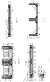
- Fig. 1 to Fig. 7 show a camera module 100 according to a preferred embodiment of the present invention.
- the camera module 100 includes a camera lens 10 and a molding photosensitive assembly 20.
- the molding photosensitive assembly 20 further includes a photosensitive element 21, a circuit board 22, a molding base 23, a set of leads 24, a supporting element 25, a plurality of electronic components 26, and a lens 27. Both ends of each of the leads 24 respectively extend to be connected to a non-photosensitive area 213 of the photosensitive element 21 and the circuit board 22, and the molding base 23 is integrally molded on the circuit board 22 so that the molding base 23, the circuit board 22, and the lens 27 forms a unitary structure.
- Each of the electronic components 26 may be attached to the circuit board 22 by a process such as an SMT (Surface Mount Technology).
- the camera lens 10 and the lens 27 are disposed on a photosensitive path of the photosensitive element 21 of the molding photosensitive assembly 20. Light reflected by the object enters inside of the camera module 100 from the camera lens 10 and the lens 27 to be subsequently received and photo-electrically converted by the photosensitive element 21, thereby acquiring an image associated with the object.
- the molding process in which the molding base 23 is molded on the thermohardening lens 27 is defined as a MOL (molding on lens) molding process so as to distinguished from the traditional COB (chip on board) molding process.
- the disposition of the lens 27 can reduce the optical TTL (a distance from a camera lens plane above a light through hole of the camera lens to a photosensitive plane of chip), thereby further reducing the size of the camera module 100 without affecting optical performance. It satisfies the demand for electronic device to equip a small-sized camera module 100.
- the disposition of the lens 27 can also reduce stain sensitivity. For example, in one embodiment, 50% of stain sensitivity can be reduced. That is, preferably, the camera lens 10 includes a plurality of camera lens elements, the camera lens element of the camera lens 10 and the lens 27 form an optical system, and light rays passing through the optical system are converged to the photosensitive element 21.
- the conventional camera lens is implemented in two parts in the present invention, one part is the camera lens 10, the other part is the lens 27, the lens 27 is a camera lens enableing to refract light, the camera lens 10 and the lens 27 play the role of refracting light together, thereby converging light to the photosensitive element 21, which can effectively reduce the TTL of the entire optical system.
- the camera lens 10 and the lens 27 form a camera lens assembly, one of the lens of the camera lens assembly becomes an external lens, that is, the lens 27, and the lens 27 is integrally packaged by the molding base 23 so that the size of the camera module can be reduced.
- the lens 27 is implemented as a lens of thermohardening properties, i.e. the lens is implemented as a thermohardening lens such that the lens 27 is capable of withstanding ambient temperature in a molding process as undergoing the molding process. For example, it is capable of withstanding a molding ambient temperature of 175 ° C in the molding process of an embodiment.
- the high temperature resistant and thermohardening lens 27 is connected to the supporting element 25 and placed together with the circuit board 22 and the photosensitive element 21 in a molding die, a solidified molding material of fluid state is around the supporting element 25 and the outer surface of the lens 27 to mold the molding base 23 molded integrally, so that the molding base 23 can be integrally molded on the circuit board 22, that is, the molding base 23, the circuit board 22 and the lens 27 forms a unitary structure.
- the lens 27 of the present invention may be not only a thermohardening lens but also a lens with other natures, and the present invention is not limited thereto.
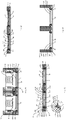
- the lens 27 includes a lens body 271 and a lens periphery 272 disposed around the lens body 271. Since the lens 27 is a precise optical element, the edge of the lens body 271 is thin.
- the lens periphery 272 disposed at the edge of the lens body 271 and integrally connected is a thickened bracket design capable of carrying the lens body 271 so as not to affect the optical performance of the lens body 271 while enabling the lens body 27 to be integrally molded to be connected to the molding base 23 in a molding die.
- the lens periphery 272 of the lens 27 is disposed in the non-photosensitive area 213 of the photosensitive element 21 before the molding base 23 is molded, the lens body 271 of the lens 27 is disposed on a photosensitive path of the photosensitive element 21 of the molding photosensitive assembly 20; after the molding base 23 is molded, the molding base 23 embeds the circuit board 22, the non-photosensitive area 213 of the photosensitive element 21, a part of the supporting element 25, and the lens periphery 272 of the lens 27 to form the molding photosensitive assembly 20.
- the supporting element 25 can effectively improve the product yield of the camera module 100 and improve the imaging quality of the camera module 100.
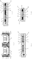
- the supporting element 25 includes an annular supporting main body 251 and has a through hole 252, wherein the supporting main body 251 is disposed on the non-photosensitive area 213 of the photosensitive element 21 such that a photosensitive area 212 of the photosensitive element 21 corresponds to the through hole 252 of the supporting element 25 and the lens body 271 of the lens 27, so that the supporting main body 251 and the lens 27 can protect the photosensitive area 212 of the photosensitive element 21 during the molding process.
- the supporting element 25 has a top surface 2501, an inner side surface 2502 and an outer side surface 2503, wherein two ends of the top surface 2501 are respectively connected to the inner side surface 2502 and the outer side surface 2503.
- a side of the supporting element 25 facing the photosensitive element 21 is defined as the inner side surface 2502 of the supporting element 25, and a side of the supporting element 25 facing the circuit board 22 is defined as the outer side surface 2503 of the supporting element 25.
- the inner side surface 2502 of the supporting element 25 is used to form the through hole 252 of the supporting element 25.
- the lens periphery 272 has a top surface 2721, a bottom surface 2722 and an outer peripheral surface 2723. Two ends of the outer peripheral surface 2733 of the lens periphery 272 are respectively connected to the top surface 2721 and the bottom surface 2722 of the lens periphery 272. That is, a side of the lens periphery 272 facing the circuit board 22 is defined as the outer peripheral surface 2723 of the lens periphery 272. It is to be noted that the lens body 271 has an outer lens surface 2711 and an inner lens surface 2712.
- a side of the lens body 271 facing the photosensitive element 21 is defined as the inner lens surface 2712 of the lens body 271, and a side connected to the top surface 2721 of the lens periphery 272 is defined as the outer lens surface 2711 of the lens body 271.
- the lens 27 is attached to the supporting main body 251, it is placed in a molding die together with the circuit board 22 and the photosensitive element 21 to perform a molding process.
- Thermocuring molding material of fluid state is thermally cured to form the molding base 23, and the molding base 23 embeds the outer side surface 2503 of the supporting main body 251 and the outer peripheral surface 2723 of the lens periphery 271 after being molded.
- the molding base 23 embeds all or a part of the top surface 2721 of the lens periphery 271 after being molded.
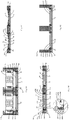
- the photosensitive element 21 includes the photosensitive area 212 and the non-photosensitive area 213, wherein the photosensitive area 212 and the non-photosensitive area 213 of the photosensitive element 21 are integrally formed, and the photosensitive area 212 is located in the center of the photosensitive element 21, the non-photosensitive area 213 is located at outer part of the photosensitive element 21, and the non-photosensitive area 213 surrounds the photosensitive area 212.
- the photosensitive area 212 After light reflected by an object enters inside of the camera module 100 from the camera lens 10, it can be received and photo-electrically converted by the photosensitive area 212 of the photosensitive element 21 to acquire an image associated with the object.
- the photosensitive element 21 has a set of chip connectors 211
- the circuit board 22 has a set of circuit board connectors 221, wherein both ends of each of the leads 24 can be respectively connected to each of the chip connectors 211 of the photosensitive element 21 and each of the circuit board connectors 221 of the circuit board 22, the photosensitive element 21 and the circuit board 22 are connected in such a manner as described above.
- each of the chip connectors 211 of the photosensitive element 21 and each of the circuit board connectors 221 of the circuit board 22 may be a connection disk, that is, each of the chip connectors 211 of the photosensitive element 21 and each of the circuit board connectors 221 of the circuit board 22 may be respectively in a disk shape for connecting both ends of each of the leads 24 to each of the chip connectors 211 of the photosensitive element 21 and each of the circuit board connectors 221 of the circuit board 22.
- each of the chip connectors 211 of the photosensitive element 21 and each of the circuit board connectors 221 of the circuit board 22 may be spherical, for example, a solder paste or other solder material is spotted on the photosensitive element 21 and the circuit board 22 to form the chip connector 211 of the photosensitive element 21 and the circuit board connector 221 of the circuit board 22, respectively.
- the shape of the chip connector 211 of the photosensitive element 21 and the circuit board connector 221 of the circuit board 22 are not limit in the content and scope of the present invention.
- each of the chip connectors 211 of the photosensitive element 21 is disposed in the non-photosensitive area 213 of the photosensitive element 21.
- the non-photosensitive area 213 of the photosensitive element 21 has a chip inner side portion 2131, a chip connection portion 2132, and a chip outer side portion 2133, wherein the chip inner side portion 2131 surrounds the photosensitive area 212, both ends of the chip connection portion 2132 extend and are connected to the chip inner side portion 2131 and the chip outer side portion 2132, respectively.
- an area of the non-photosensitive area 213 from the position where the chip connector 211 is disposed to the position of an edge of the photosensitive area 212 is defined as the chip inner side portion 2131
- an area of the non-photosensitive area where the chip connector 211 is disposed is defined as the chip connection portion 2132
- an area of the non-photosensitive area 213 from the position where the chip connector 211 is disposed to the position of the outer edge of the photosensitive element 21 is defined as the chip outer side portion 2132.
- the photosensitive element 21 is, in order from the outside to the inside, the chip outer side portion 2133, the chip connection portion 2132, the chip inner side portion 2131 and the photosensitive area 212.
- the circuit board 22 includes a flat chip attaching area 222 and an edge area 223, wherein the edge area 223 is integrally formed with the chip attaching area 222, and the edge area 223 is located on the periphery of the chip attaching area 222.
- the chip attaching area 222 is used to attach the photosensitive element 21, and the circuit board connector 221 is disposed in the edge area 223.
- the edge area 223 of the circuit board 22 has a circuit board inner side portion 2231, a circuit board connection portion 2232, and a circuit board outer side portion 2233, wherein the circuit board inner side portion 2231 surrounds the chip attaching area 222.
- Both ends of the circuit board connection portion 2232 respectively extend and are connected to the circuit board inner side portion 2231 and the circuit board outer side portion 2233. That is, the area of the edge area 223 from a position where the circuit board connector 221 is disposed to a position of an edge of the chip attaching area 222 is defined as the board inner side portion 2231, the area of the edge area 223 where the circuit board connector 221 is disposed is defined as the circuit board connection portion 2232, and the area of the edge area 223 from the position where the circuit board connector 221 is disposed to the position of the outer edge of the edge area 223 is defined as the circuit board outer side portion 2233.
- the circuit board 22 is, in order from the outside to the inside, the circuit board outer side portion 2233, the circuit board connection portion 2232, the circuit board inner side portion 2231 and the chip attaching area 222.
- the type of the lead 24 is not limited in the camera module 100 of the present invention.
- the lead 24 can be implemented as a gold wire, that is, the photosensitive element 21 and the circuit board 22 can be connected together by a gold wire, so that the electrical signal can be further transmitted to the circuit board 22 through the lead 24 after the photosensitive element 21 converts an optical signal into an electrical signal.
- the lead 24 can also be implemented as any material capable of realizing the transmission of the electrical signal between the photosensitive element 21 and the circuit board 22.
- each of the electronic components 26 is attached to the edge area 223 of the circuit board 22.
- each of the electronic components 26 is attached to the circuit board outer side portion 2233 of the edge area 223.
- the photosensitive element 21 and each of the electronic components 26 may be attached to the same side or opposite sides of the circuit board 22, for example, in a specific embodiment, the photosensitive element 21 and each of the electronic components 26 is attached to the same side of the circuit board 22, and the photosensitive element 21 is attached to the chip attaching area 222 of the circuit board 22, and each of the electronic components 26 is attached to the edge area 223 of the circuit board 22.
- the molding base 23 embeds each of the electronic components 26 to isolate adjacent ones and isolate the electronic component 26 and the photosensitive element 21, so that in the camera module 100 of the present invention, even when the distance between the adjacent electronic components 26 is relatively close, the molding base 23 can prevent adjacent electronic components 26 from contacting or interfering with each other, and the manner in which the molding base 23 embeds the electronic component 26 can also prevent contaminants generated on the surface of the electronic component 26 from contaminating the photosensitive area 212 of the photosensitive element 21, thereby reducing the volume of the camera module 100 and improving the imaging quality of the camera module 100.
- the manner in which the molding base 23 embeds the electronic component 26 in the camera module 100 of the present invention makes the circuit board 22 of a small area to be capable of being attached more electronic component 26.
- the types of electronic components 26 include, but are not limited to, resistors, capacitors, drivers and the like.
- the camera module 100 further includes at least one filter element 40.
- the filter element 40 is disposed at the bottom of the camera lens 10. That is, the filter element 40 is assembled to the camera lens 10. The optical lens inside the camera lens 10 are sequentially arranged, and the filter element 40 is located in the optical path of the camera lens 10. After the molding photosensitive assembly 20 is molded and integrally packaged, the filter element 40 and the camera lens 10 are attached to the molding photosensitive assembly 20 to be assembled to form the camera module 100. The filter element 40 is located in the photosensitive path of the photosensitive element 21.
- the light reflected by the object which is from the optical lens of the camera lens 10 and filtered by the filter element 40 to enter the inside of the camera module 100, can be received and photo-electrically converted by the photosensitive element 21. That is, the filter element 40 can filter stray light, such as an infrared part, from the light reflected by the object in each of the optical lens of the camera lens 10, and in this manner, the imaging quality of the camera module 100 can be improved.
- the filter elements 40 can be implemented in different types, for example, the filter elements 40 can be implemented as infrared cut filters, a full transmissive spectral filter and other filters, or a combination of a plurality of filters, for example, the filter element 40 can be implemented as a combination of an infrared cut filter and a full transmissive spectral filter.
- the infrared cut filter and the full transmissive spectral filter can be switched to be selectively located on the photosensitive path of the photosensitive element 21, for example, when the camera module 100 is used in a light sufficient environment such as daytime, the infrared cut filter can be switched to the photosensitive path of the photosensitive element 21 to filter infrared rays from the light reflected by the object that enters the camera module 100 through the infrared cut filter, when the camera module 100 is used in a dark environment such as at night, the full transmissive spectral filter may be switched to the photosensitive path of the photosensitive element 21 to allow the transmittion of the infrared portion of the light reflected by the object that enters the camera module 100.
- the mounting position of the filter element 40 has various variant embodiments in different embodiments.
- the filter element 40 described in Fig. 7 is disposed at the bottom part inside the camera lens 10.
- the filter element 40 is disposed at top of the molding base 23. Both of these dispositions are performed by mounting the filter element 40 after the molding photosensitive assembly 20 is molded integrally.
- the filter element 40 and the molding photosensitive assembly 20 are molded and assembled together in a molding die. That is, in other embodiments, the peripheral edge of the filter element 40 may be covered by the supporting element 25 and secured between the photosensitive element 21 and the lens 27.
- the filter element 40 is attached to the photosensitive element 21 and located between the lens 27 and the photosensitive element 21.
- the latter two dispositions are in that the filter element 40 and the photosensitive element 21, the circuit board 22, the supporting element 25 and the lens 27 are placed together in a molding die, the molding base 23 is formed after being molded by the MOL process, so as to being assembled to form the camera module 100 after the camera lens 10 or a driver 30 driving the camera lens 10 is mounted.
- Various variations in position of the filter element 40 will be disclosed in detail in subsequent embodiments.
- the lens 27 can be a convex lens and has a function of converging light. Since the filter element 40 does not cause refraction of light, the lens 27 implemented as a convex lens makes image smaller. The particles (stains) on the filter element 40 tend to cause the photosensitive element 21 to form a large stain point in the image, and the closer to the photosensitive element 21, the larger the imaged stain point is. Therefore, in the MOL process of the present invention, the lens 27 is disposed at a lower part of the camera lens 10, and the filter element 40 is disposed at a bottom portion inside the camera lens 10. That is, the MOL process of the present invention can move the filter element away from the photosensitive element 21 without affecting the convergence of the light of the lens 27 implemented as a convex lens, thereby making the image of the stained spot smaller.
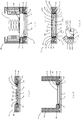
- the lens periphery 272 of the lens 27 has a square step shape.
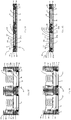
- the supporting main body 251 also has various variant embodiments.
- the supporting main body 251 covers entire of the lead 24, the circuit board outer side portion 2233 of the edge area 223, the circuit board connection portion 2232, the circuit board inner side portion 2231, the chip outer side portion 2133, the chip connection portion 2132 and the chip inner side portion 2131 of the non-photosensitive area 213; and in another embodiment, the supporting main body 251 covers a part of the lead 24, the chip outer side portion 2133, the chip connection portion 2132 and the chip inner side portion 2131 of the non-photosensitive area 213; and in another embodiment, the supporting main body 251 covers a part of the lead 24, the circuit board inner side portion 2231 of the edge area 223, the chip outer side portion 2133, the chip connection portion 2132 and the chip inner side portion 2131 of the non-photosensitive area 213; and for example, in an embodiment, The supporting main body 251 covers a part of the lead 24, the circuit board outer side portion 2233 of the edge area 223, the circuit board connection portion 2232, the circuit board inner
- the camera module 100 can be implemented as a fixed focus camera module, wherein the camera module 100 maintains the camera lens 10 in a photosensitive path of the photosensitive element 21 by a molding body 232 assembled to the molding base 23. It is to be noted that, in an embodiment, the camera module 100 can be implemented as a zoom camera module, wherein the camera module 100 changes the distance between the camera lens 10 and the photosensitive element 21 to adjust the focal length of the camera module.
- the camera module 100 is implemented as a zoom camera module as shown in Fig. 7 .
- the camera module 100 further includes the driver 30, wherein the camera lenses 10 are respectively disposed correspondingly to the drivers 30, the drivers 30 are respectively assembled to the molding bases 23, and the drivers 30 are electrically connected to the circuit board 22, respectively, to enable the driver 30 to drive the camera lens 10 to move back and forth along the photosensitive path of the photosensitive element 21 after the circuit board 22 transmits power and control signals to the driver 30 so as to adjust the focal length of the camera module 100. That is, the camera lens 10 is drivably disposed to the driver 30. It is to be noted that the type of the driver 30 is not limited in the camera module 100 of the present invention.
- the driver 30 can be implemented as any driver, such as a voice coil motor, that is capable of driving the camera lens 10 along the photosensitive path of the photosensitive element 21 to generate a displacement, wherein the driver 30 is capable of receiving electrical energy and control signals to be in an operational state.
- a voice coil motor that is capable of driving the camera lens 10 along the photosensitive path of the photosensitive element 21 to generate a displacement
- the driver 30 is capable of receiving electrical energy and control signals to be in an operational state.
- the molding body 232 is implemented as a lens bracket for assembling the camera lens 10
- the camera lens 10 is directly mounted on the molding body 232 which is implemented as a lens bracket after the photosensitive element 20 is integrally formed, thereby simplifying the assembly process of the camera module 100. Variations of this aspect of the present invention will be disclosed in detail in the following embodiments.
- the molding photosensitive assembly 20 is integrally formed by the MOL molding process and assembled to form the camera module 100 are disclosed in detail from the respective embodiments.
- the bottom surface 2722 of the lens 27 is attached to the top surface 2501 of the supporting element 25, and the supporting main body 251 covers entire of the lead 24, the circuit board outer side portion 2233, the circuit board connection portion 2232 and the circuit board inner side portion 2231 of the edge area 223, and the chip outer side portion 2133, the chip connection portion 2132 and the chip inner side portion 2131 of the non-photosensitive area 213, the filter element 40 is disposed at a bottom portion inside the camera lens 10.
- the camera lens 10 is mounted after the molding photosensitive assembly 20 is integrally molded.
- the manufacturing steps of the camera module 100 and the manufacturing steps of the molding photosensitive assembly 20 will be described.
- the photosensitive element 21 is attached to the chip attaching area 222 of the circuit board 22, and the chip connector 211 of the non-photosensitive area 213 of the photosensitive element 21 and the circuit board connector 221 of the edge area 223 of the circuit board 22 is connected by a set of the leads 24.
- the electronic component 26 is attached to the circuit board outer side portion 2233 of the edge area 223 of the circuit board 22.
- both ends of a set of the leads 24 are respectively connected to the photosensitive element 21 and the circuit board 22, wherein each of the leads 24 protrudes arcually from the upper surface of the photosensitive element 21, and the curved curvature of the lead 24 is maintained in a rounded state, which is advantageous for ensuring the ability of the lead 24 to transmit the electrical signal between the photosensitive element 21 and the circuit board 22, wherein each of the leads 24 is arranged between the photosensitive element 21 and the circuit board 22, for example, each of the leads 24 may be equally spaced.
- a plurality of the photosensitive elements 21 may be attached to different positions of one circuit board 22 to subsequently fabricate a dual lens camera module or array camera module, for example, in a embodiment shown in Fig. 14 , a plurality of the circuit boards 22 are placed together to form a circuit board jointed board 2200, and then each of the photosensitive elements 21 is respectively attached to the circuit board 22 at a corresponding position of the circuit board jointed board to subsequently separate the circuit board jointed board 2200, but the present invention is not limited in this respect.
- the supporting main body 251 can prevent the connection position of the lead 24 and the chip connector 211 from coming into contact with the thermocuring material for forming the molding base 23, so as to prevent the thermocuring material of fluid state from causing deformation of the end of the lead 24 for connecting the chip connector 211 or the detachment of the lead 24 from the chip connector 211.
- the supporting main body 251 and the lens periphery 272 of the lens 27 are connected together to isolate the connection position of the lead 24 and the chip connector 211 from the thermocuring material.
- the supporting main body 251 and the lens periphery 272 of the lens 27 are connected together, the inner side surface 2502 of the supporting element 25 and the lens inner surface 2712 of the lens body 271 form a closed space 2700, such that when the MOL molding process is performed, the thermocuring material of fluid state is prevented from entering the closed space 2700, thereby avoiding affecting the light-passing path and also reducing the stain sensitivity.
- the supporting main body 251 may be formed by disposing glue at the non-photosensitive area 213 of the photosensitive element 21 and formed after the glue is initially cured. After the preliminary curing, the lens 27 is further disposed and further cured to finally form the supporting main body 251.
- the inner side surface 2502 of the supporting main body 251 forms the through hole 252, and the photosensitive area 212 of the photosensitive element 21 corresponds to the through hole 252 and the lens body 271 of the thermohardening lens 27.
- the supporting main body 251 formed of glue may also have a viscosity for subsequently adhering contaminants such as dust, thereby preventing the contaminants from contaminating the photosensitive area 212 of the photosensitive element 21 to cause the occurance of a stain point in the photosensitive area 212 of the photosensitive element 21 to further ensure the image quality of the camera module.
- the lens periphery 272 of the lens 27 is attached to the supporting main body 251 of the supporting element 25 after the supporting element 25 is fully cured, and the present invention is not limited thereto.
- the molding material of the thermocuring material which is implemented in fluid state is formed into the molding base 23 which is at least integrally molded on the circuit board 22 after curing by a molding die 900.
- the size of the camera module 100 and the assembly error of the camera module can be reduced, thereby making the structure of the camera module 100 more compact and improving the image quality of the camera module 100.
- the lens 27 is disposed on the photosensitive element 21 through the supporting element 25, the optical TTL is reduced, the structure of the camera module 100 is more compact, and the size of the camera module 100 of the electronic device is satisfied.
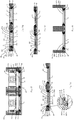
- the molding die 900 includes an upper die 901 and a lower die 902, wherein at least one of the upper die 901 and the lower die 902 can be moved to enable the upper die 901 and the lower die 902 to be clamped, and at least one molding space 903 is formed between the upper die 901 and the lower die 902, wherein the molding base 23 is formed by adding the molding material to the molding space 903 after curing.
- the photosensitive element 21 and the circuit board 22 are connected by a set of the leads 24, the supporting main body 251 is formed on the non-photosensitive area 213 of the photosensitive element 21 to cover entire of the lead 24, the circuit board outer side portion 2233, the circuit board connection portion 2232 and the circuit board inner side portion 2231 of the edge area 223, the chip outer side portion 2133, the chip connection portion 2132 and the chip inner side portion 2132 of the non-photosensitive area 213, the lens 27 is disposed on the supporting main body 251, so that a semi-finished product of the molding photosensitive assembly 20 is fabricated, the semi-finished product of the molding photosensitive assembly 20 is placed on the lower die 902 of the molding die 900, the upper die 901 and/or the lower die 901 of the molding die 900 are operated, so that the upper die 901 and the lower die 902 are clamped, thereby the molding space 903 is formed between the upper die 901 and the lower die 902, wherein the press-fitted surface 9011 of the upper die 901 is in contact with lens inner
- the exterior of the circuit board 22, the non-photosensitive area 213 of the photosensitive element 21, a part of the supporting element 25 and the outer peripheral surface 2723 of the lens periphery 272 of the lens 27 are located in the molding space 903 of the molding die 900, so that when the molding base 23 is molded in the molding space 903, the molding base 23 embeds the exterior of the circuit board 22, the non-photosensitive area 213 of the photosensitive element 21, a part of the supporting element 25 and the outer peripheral surface 2723 of the lens periphery 272.
- the molding photosensitive assembly 20 formed as shown in Fig.
- the molding base 23 formed also covers a part of the top surface 2721 of the lens periphery 272.
- the molding space 903 of the molding die 900 may be an annular space to form a annular molding base 23 after the molding material is added to the molding space 903 and cured.
- the fluid-state molding material according to the present invention may be a liquid material or a solid particulate material or a mixed material of liquid and solid particles. It is to be understood that whether the molding material is implemented as a liquid material or as a solid particulate material or as a mixed material of liquid and solid particles, after being added to the molding space 903 of the molding die 900, it can be cured to form the molding base 23.
- the fluid-state molding material is implemented as a thermocuring material such as a liquid, wherein the molding material is cured after being added to the molding space 903 of the molding die 900 to form the molding base 23. It is to be noted that, when the fluid-state molding material is added to the molding space 903 of the molding die 900, the curing manner of the fluid-state molding material does not limit the content and scope of the present invention.
- the medium forming the supporting element 25 and the medium forming the molding base 23 are of different materials.
- the supporting element 25 can be formed by an elastic medium, so that the molded supporting element 25 has a certain elasticity, and the supporting element 25 can also be formed by a rigid medium, and the present invention is not limited thereto. As shown in Fig. 5 and Fig.
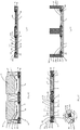
- the supporting main body 251 is disposed along the non-photosensitive area 213 of the photosensitive element 21, and the lens periphery 272 of the lens 27 is closely attached to the supporting main body 251 to form the closed space 2700 such that the supporting main body 251 and the lens body 271 of the lens 27 can prevent the molding material from entering into the closed space 2700 after the molding material is added to the molding space 903 of the molding die 900, that is, prevent it from entering the photosensitive area 212 of the photosensitive element 21, so that after the molding material is cured to form the molded base 23 and demolded, the molding base 23 is further formed into a molding hole 231 to correspond to the photosensitive area 212 of the photosensitive element 21, so that, subsequently, the molding hole 231 of the molding base 23 allows light to pass through to be received and photo-electrically converted by the photosensitive area 212 of the photosensitive element 21.
- the molding base 23 includes the molding main body 232 and has the molding hole 231 which provides a light path for the optical camera lens 10 and the photosensitive element 21. Therefore, after the light reflected by the object enters the inside of the camera module from the optical camera lens 10, the light passes through the molding hole 231 of the molding base 23 to be received and photo-electrically converted by the photosensitive area 212 of the photosensitive element 21.
- the photosensitive element 21 is first attached to the circuit board 22, and then the supporting element 25 is formed, and further, the lens 27 is disposed on the supporting element 25, the circuit board 22, the photosensitive element 21 and the lens 27 are molded to form the molding base 23, thereby be molded to form the molding photosensitive assembly 20.
- the closed space 2700 is formed between the lens 27 and the photosensitive element 21, damage of the photosensitive element 21 by the molding die can be prevented, and since the distance between the lens 27 and the photosensitive element 21 is reduced, the back focal length of the camera module 100 assembled by them can be reduced, thereby reducing the height of the camera module 100.
- the driver 30 and the camera lens 10 are assembled on the molding base 23 to form the camera module 100, wherein, in the preferred embodiment, the filter element 40 is disposed at the bottom inside the camera lens 10.
- the camera lens 10 or a lens frame supporting the camera lens 10 is directly assembled on the molding base 23, that is, the driver 30 may not be disposed.
- the driver 30 may not be disposed.
- Fig. 8B illustrates a variant embodiment based on the preferred embodiment of the present invention, illustrating that the molding photosensitive assembly 20 and the filter element 40 are assembled to form a camera module 108.
- the camera module 108 is similar in structure to the camera module 100 in the preferred embodiment, except that the filter elements 40 of the camera module 108 in Fig. 8B are disposed at different positions.
- the filter element 40 is not provided at the bottom inside the camera lens 10 of the camera module 108, but the filter element 40 is assembled on the top surface of the molding base 23, such that the filter element 40 encloses the molding hole 231 of the molding base 23, so that light entering the interior of the camera module 108 from the optical camera lens 10 can be further filtered by the filter element 40 to improve the imaging quality of the camera module 108. That is, the top surface of the molding base 23 forms an inner side surface 233 and an outer side surface 234, and in the embodiment shown in Fig.
- the plane in which the inner side surface 233 of the molding base 23 is located may be lower than the plane in which the outer side surface 234 is located, so that the top surface of the molding base 23 forms a stepped surface, that is, the plane in which the inner side surface 233 of the molding base 23 is located may be lower than the plane in which the outer side surface 234 is located to form a groove 235 of the molding base 23, wherein the filter element 40 assembled to the inner side surface 233 of the molding base 23 is accommodated within the groove 235 of the molding base 23, the driver 30 is assembled to the outer side surface 234 of the molding base 23 to enable the optical camera lens 10 assembled to the driver 30 further to be held in the photosensitive path of the photosensitive element 21, thereby producing the camera module 108.
- the inner side surface 233 and the outer side surface 234 of the molding base 23 are in a same plane to allow the top surface of the molding base 23 to form a flat plane, wherein the filter element 40 is assembled to the inner side surface 233 of the molding base 23, the driver 30 or the camera lens 10 is assembled to the outer side surface 234 of the molding base 23, or the camera lens 10 is assembled directly to the outer side surface 234 of the molding base 23.
- the above structure of the molding base 23 of the present invention is merely an example, and the present invention is not limited thereto.
- the photosensitive element 21 is first attached to the circuit board 22, and then the supporting element 25 is formed, and further, the lens 27 is disposed on the supporting element 25, such that the circuit board 22, the photosensitive element 21 and the lens 27 are molded in a molding die to form the molding base 23, thereby forming the molding photosensitive assembly 20. Further, the driver 30 and the camera lens 10 are assembled after the filter element 40 is assembled to the top surface of the molding base 23, thereby assembling and forming the camera module 108.
- a camera module 109 according to another variant embodiment of the preferred embodiment of the present invention is described, the camera module 109 in the variant embodiment and the camera module 100 in the preferred embodiment are similar in structure, except that the disposition and assembly order of the filter elements 40 of the camera module 109 in Fig. 9 are different.
- the molding photosensitive assembly 20 is molded first, and then the filter element 40 disposed at the bottom of the camera lens and the camera lens 10 are assembled together on the molding base 23.
- the filter element 40, the lens 27, the supporting element 25, the photosensitive element 21 and the circuit board 22 are placed together in a molding die to form the molding base 23, and then the driver 30 and the camera lens 10 are attached to the molding base 23.
- the filter element 40 is laminated on the photosensitive element 21.
- a surface attach process can be used here.
- the edge of the filter element 40 is fixedly connected by the supporting element 25 and attach to the photosensitive element 21, thereby The filter element 40 is fixed between the supporting element 25 and the photosensitive element 21.
- the outer side surface 2503 of the supporting main body 251, the outer peripheral surface 2723 of the lens periphery 272 are molded to the molding base 23, the supporting element 25, the photosensitive element 21 and the lens 27, the circuit board 22 and the electronic component 26 are molded by the molding main body 232 of the molding base 23.
- the filter element 40 covers the photosensitive element 21, and the photosensitive element 21 is isolated from the closed space 2700 and the external environment, thereby, the photosensitive element 21 is prevented from being damaged and dust entering the closed space 2700 is prevented from coming into contact with the photosensitive member 21, and stain sensitivity is lowered.
- the photosensitive element 21 is attached to the circuit board 22 firstly, and the filter element 40 is attached to the photosensitive element 21, and then the supporting element 25 is formed, and the supporting element 25 is connected to both ends of the filter element 40.
- the lens 27 is disposed on the supporting element 25, the circuit board 22, the photosensitive element 21 and the lens 27 is molded to form the molding base 23.
- the closed space 2700 is formed between the lens 27 and the filter element 40, damage of the molding die to the photosensitive element 21 and the filter element 40 can be prevented.
- the distance between the filter element 40 and the photosensitive element 21 is reduced, the back focus of the camera module 109 assembled by them can be reduced, thereby reducing the height of the camera module 109.
- the thickness of the camera module 109 is further reduced to some extent, since it is not necessary to provide additional supporting component for the filter element 40.
- Fig. 10 shows a camera module 110 based on another variant embodiment of the preferred embodiment shown in Fig. 7 .
- the structure of the molding main body 232 of the molding base 23 is different.
- the molding base 23 of the camera module 110 includes the molding main body 232 and a camera lens mounting section 236, the molding main body 232 and the camera lens mounting section 236 are integrally molded to be connected in sequence.
- the camera lens mounting section 236 is for mounting the camera lens 10 (the camera lens 10 is not shown in Fig.
- the camera lens 10 that is, when the molding photosensitive assembly 20 is used to assemble the camera module 110, the camera lens 10 is mounted at an inner side of the camera lens mounting section 236 to provide a stable mounting position for the camera lens 10.
- the camera lens mounting section 236 extends integrally upwardly to provide a support fixed position for the camera lens 10 so that no additional components need to be provided to mount the camera lens 10.
- the molding base 23 integrally extends upwardly and is internally stepped to mold the lens 27, the supporting element 25, the circuit board 22 and the electronic component 26 respectively, and to support the camera lens 10.
- the inner side surface of the camera lens mounting section 236 is flat, so as to be suitable for mounting the unthreaded camera lens 10 to form a fixed focus module.
- the camera lens 10 can be fixed to the camera lens mounting section 236 by adhesive bonding. It is also to be noted that the camera lens 10 is mounted on the camera lens mounting section 236 such that the molding base 23 functions as a bracket or a lens barrel in a conventional camera module, and provides a supporting and fixing position for the camera lens 10, but assembly is different from the traditional COB process.
- the bracket of the camera module of the conventional COB process is fixed to the circuit board in a pasting manner, and the molding base 23 is fixed to the circuit board 22, the supporting element 25 and the lens 27 by an MOL molding process.
- the molding method has better connection stability and the controllability of the process with respect to the paste fixing, so that the thickness of the camera module is reduced, and further, the molding base 23 replaces the conventional bracket to provide the mounting position of the camera lens 10, which avoids the tilt error caused by the bracket during the assembly, and reduces the cumulative tolerance of the assembly of the camera module.
- the filter element 40 when the filter element 40 needs to be mounted, the filter element 40 may be disposed at the bottom portion of the camera lens 10 in the camera module 100 as described in Fig. 7 , it may also be directly mounted on the inner side surface 233 of the molding main body 232 of the molding base 23, as the camera module 108 described in Fig. 8B , and it may also be attached to the surface of the photosensitive element 21 by the supporting element 25 before being molded to form the molding base 23 as shown in Fig. 9 .
- the present invention is not limited thereto.
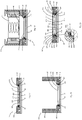
- Fig. 15 shows a camera module 115 according to another variant embodiment of the preferred embodiment of the present invention, which is different from the camera module 100 in the preferred embodiment described in Fig. 7 in that, the supporting main body 251 of the molding photosensitive assembly 20 of the camera module 115 embeds a part of the lead 24, the chip outer side portion 2133, the chip connection portion 2132 and the chip inner side portion 2131 of the non-photosensitive area 213.
- the molding main body 232 is integrally molded to embed the electronic component 26, the edge area 223 of the circuit board 22, the outer side 2503 of the supporting element 25 and the outer peripheral surface 2723 of the lens periphery 272, thereby forming the molding photosensitive assembly 20. It will be understood that the molding main body 232 may also embed a part or all of the top surface 2721 of the lens periphery 272 to enhance the stability of the lens 27.
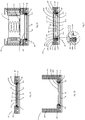
- Fig. 16 shows a camera module 116 based on another variant embodiment of the embodiment of Fig. 8B , which is different from the camera module 108 in the embodiment of Fig. 8B in that, the supporting main body 251 of the molding photosensitive assembly 20 of the camera module 116 of the present invention embeds a part of the lead 24, the chip outer side portion 2133, the chip connection portion 2132 and the chip inner side portion 2131 of the non-photosensitive area 213.
- the molding main body 232 is integrally molded to embed the electronic component 26, the edge area 223 of the circuit board 22, the outer side surface 2503 of the supporting element 25, and the outer peripheral surface 2723 of the lens periphery 272, thereby forming the molding photosensitive assembly 20. It will be understood that the molding main body 232 may also embed a part or all of the top surface 2721 of the lens periphery 272 to enhance the stability of the lens 27.
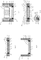
- Fig. 17 shows a camera module 117 based on another variant embodiment of the embodiment of Fig. 9 , which is different from the camera module 109 in the embodiment of Fig. 9 in that, the supporting main body 251 of the molding photosensitive assembly 20 of the camera module 117 of the present invention embeds a part of the lead 24, the chip outer side portion 2133, the chip connection portion 2132 and the chip inner side portion 2131 of the non-photosensitive area 213.
- the molding main body 232 is integrally molded to embed the electronic component 26, the edge area 223 of the circuit board 22, the outer side surface 2503 of the supporting element 25, and the outer peripheral surface 2723 of the lens periphery 272, thereby forming the molding photosensitive assembly 20. It will be understood that the molding main body 232 may also embed a part or all of the top surface 2721 of the lens periphery 272 to enhance the stability of the lens 27.
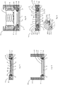
- Fig. 18 shows a camera module 118 based on another variant embodiment of the embodiment of Fig. 10 , which is different from the camera module 110 in the embodiment of Fig. 10 in that, the supporting main body 251 of the molding photosensitive assembly 20 of the camera module 118 of the present invention embeds a part of the lead 24, the chip outer side portion 2133, the chip connection portion 2132 and the chip inner side portion 2131 of the non-photosensitive area 213.
- the molding main body 232 is integrally molded to embed the electronic component 26, the edge area 223 of the circuit board 22, the outer side surface 2503 of the supporting element 25, and the outer peripheral surface 2723 of the lens periphery 272, thereby forming the molding photosensitive assembly 20. It will be understood that the molding main body 232 may also embed a part or all of the top surface 2721 of the lens periphery 272 to enhance the stability of the lens 27.
- Fig. 19 shows a camera module 119 based on another variant embodiment of the preferred embodiment of the present invention, which is different from the camera module 100 in the preferred embodiment described in Fig. 7 in that, the supporting main body 251 embeds a part of the lead 24, the circuit board inner side portion 2231 of the edge area 223, the chip outer side portion 2133, the chip connection portion 2132 and the chip inner side portion 2131 of the non-photosensitive area 213.
- the molding main body 232 is integrally molded to embed the electronic component 26, the edge area 223 of the circuit board 22, the outer side surface 2503 of the supporting element 25, and the outer peripheral surface 2723 of the lens periphery 272, thereby forming the molding photosensitive assembly 20. It will be understood that the molding main body 232 may also embed a part or all of the top surface 2721 of the lens periphery 272 to enhance the stability of the lens 27.
- Fig. 20 shows a camera module 120 based on another variant embodiment of the preferred embodiment of the present invention, which is different from the camera module 108 in the embodiment shown in Fig. 8B in that, the supporting main body 251 embeds a part of the lead 24, the circuit board inner side portion 2231 of the edge area 223, the chip outer side portion 2133, the chip connection portion 2132 and the chip inner side portion 2131 of the non-photosensitive area 213.
- the molding main body 232 is integrally molded to embed the electronic component 26, the edge area 223 of the circuit board 22, the outer side surface 2503 of the supporting element 25, and the outer peripheral surface 2723 of the lens periphery 272, thereby forming the molding photosensitive assembly 20. It will be understood that the molding main body 232 may also embed a part or all of the top surface 2721 of the lens periphery 272 to enhance the stability of the lens 27.
- Fig. 21 shows a camera module 121 based on another variant embodiment of the preferred embodiment of the present invention, which is different from the camera module 109 in the embodiment shown in Fig. 9 in that, the supporting main body 251 embeds a part of the lead 24, the circuit board inner side portion 2231 of the edge area 223, the chip outer side portion 2133, the chip connection portion 2132 and the chip inner side portion 2131 of the non-photosensitive area 213.
- the molding main body 232 is integrally molded to embed the electronic component 26, the edge area 223 of the circuit board 22, the outer side surface 2503 of the supporting element 25, and the outer peripheral surface 2723 of the lens periphery 272, thereby forming the molding photosensitive assembly 20. It will be understood that the molding main body 232 may also embed a part or all of the top surface 2721 of the lens periphery 272 to enhance the stability of the lens 27.
- Fig. 22 shows a camera module 122 based on another variant embodiment of the preferred embodiment of the present invention, which is different from the camera module 110 in the embodiment shown in Fig. 10 in that, the supporting main body 251 embeds a part of the lead 24, the circuit board inner side portion 2231 of the edge area 223, the chip outer side portion 2133, the chip connection portion 2132 and the chip inner side portion 2131 of the non-photosensitive area 213.
- the molding main body 232 is integrally molded to embed the electronic component 26, the edge area 223 of the circuit board 22, the outer side surface 2503 of the supporting element 25, and the outer peripheral surface 2723 of the lens periphery 272, thereby forming the molding photosensitive assembly 20. It will be understood that the molding main body 232 may also embed a part or all of the top surface 2721 of the lens periphery 272 to enhance the stability of the lens 27.
- Fig. 23 shows a camera module 123 based on another variant embodiment of the preferred embodiment of the present invention, which is different from the camera module 100 in the embodiment shown in Fig. 7 in that, the supporting main body 251 embeds a part of the lead 24, the circuit board outer side portion 2233, the circuit board connection portion 2232 and the circuit board inner side portion 2231 of the edge area 223.
- the molding main body 232 is integrally molded to embed the electronic component 26, the circuit board outer side portion 2233 of the edge area 223 of the circuit board 22, the outer side surface 2503 of the supporting element 25, and the outer peripheral surface 2723 of the lens periphery 272, thereby forming the molding photosensitive assembly 20.
- the molding main body 232 may also embed a part or all of the top surface 2721 of the lens periphery 272 to enhance the stability of the lens 27.
- Fig. 24 shows a camera module 124 based on another variant embodiment of the preferred embodiment of the present invention, which is different from the camera module 108 in the embodiment shown in Fig. 8B in that, the supporting main body 251 embeds a part of the lead 24, the circuit board outer side portion 2233, the circuit board connection portion 2232 and the circuit board inner side portion 2231 of the edge area 223.
- the molding main body 232 is integrally molded to embed the electronic component 26, the circuit board outer side portion 2233 of the edge area 223 of the circuit board 22, the outer side surface 2503 of the supporting element 25, and the outer peripheral surface 2723 of the lens periphery 272, thereby forming the molding photosensitive assembly 20.
- the molding main body 232 may also embed a part or all of the top surface 2721 of the lens periphery 272 to enhance the stability of the lens 27.
- Fig. 25 shows a camera module 125 based on another variant embodiment of the preferred embodiment of the present invention, which is different from the camera module 109 in the embodiment shown in Fig. 9 in that, the supporting main body 251 embeds a part of the lead 24, the circuit board outer side portion 2233, the circuit board connection portion 2232 and the circuit board inner side portion 2231 of the edge area 223.
- the molding main body 232 is integrally molded to embed the electronic component 26, the circuit board outer side portion 2233 of the edge area 223 of the circuit board 22, the outer side surface 2503 of the supporting element 25, and the outer peripheral surface 2723 of the lens periphery 272, thereby forming the molding photosensitive assembly 20.
- the molding main body 232 may also embed a part or all of the top surface 2721 of the lens periphery 272 to enhance the stability of the lens 27.
- the structure of the camera module 125 and the camera module 109 in the embodiment shown in Fig. 9 is different in that the filter element 40 is not attached to the photosensitive element 21. That is, since the supporting main body 251 does not embed the non-photosensitive area 213, the edge of the filter element 40 is embeded on a position of an upper end of the supporting main body 251 near the top surface 2501 to avoid contacting the lead 24, and thus the filter element 40 and the photosensitive element 21 are gapped. It can be understood by those skilled in the art that in other variant embodiments of the embodiment shown in Fig. 25 , the edge of the filter element 40 may not be fixed by being embeded by the supporting main body 251, but the filter element 40 is directly attached to the photosensitive area 212 of the photosensitive element 21, but the present invention is not limited in this respect.
- Fig. 26 shows a camera module 126 based on another variant embodiment of the preferred embodiment of the present invention, which is different from the camera module 110 in the embodiment shown in Fig. 10 in that, after the MOL molding process, the molding main body 232 is integrally molded to embed the electronic component 26, the circuit board outer side portion 2233 of the edge area 223 of the circuit board 22, the outer side surface 2503 of the supporting element 25, and the outer peripheral surface 2723 of the lens periphery 272, thereby forming the molding photosensitive assembly 20. It will be understood that the molding main body 232 may also embed a part or all of the top surface 2721 of the lens periphery 272 to enhance the stability of the lens 27.
- Fig. 27 shows a camera module 127 based on another variant embodiment of the preferred embodiment of the present invention, which is different from the camera module 100 in the preferred embodiment described in Fig. 7 in that, the supporting main body 251 embeds a part of the lead 24, the circuit board outer side portion 2233, the circuit board connection portion 2232 and the circuit board inner side portion 2231 of the edge area 223, and the outer side portion of the non-photosensitive area 213.
- the molding main body 232 is integrally molded to embed the electronic component 26, the circuit board outer side portion 2233 of the edge area 223 of the circuit board 22, the outer side surface 2503 of the supporting element 25, and the outer peripheral surface 2723 of the lens periphery 272, thereby forming the molding photosensitive assembly 20.
- the molding main body 232 may also embed a part or all of the top surface 2721 of the lens periphery 272 to enhance the stability of the lens 27.
- Fig. 28 shows a camera module 128 based on another variant embodiment of the preferred embodiment of the present invention, which is different from the camera module 108 in the embodiment shown in Fig. 8B in that, the molding main body 232 is integrally molded to embed the electronic component 26, the circuit board outer side portion 2233 of the edge area 223 of the circuit board 22, the outer side surface 2503 of the supporting element 25, and the outer peripheral surface 2723 of the lens periphery 272, thereby forming the molding photosensitive assembly 20. It will be understood that the molding main body 232 may also embed a part or all of the top surface 2721 of the lens periphery 272 to enhance the stability of the lens 27.
- Fig. 29 shows a camera module 129 based on another variant embodiment of the preferred embodiment of the present invention, which is different from the camera module 109 in the embodiment shown in Fig. 9 in that, the molding main body 232 is integrally molded to embed the electronic component 26, the circuit board outer side portion 2233 of the edge area 223 of the circuit board 22, the outer side surface 2503 of the supporting element 25, and the outer peripheral surface 2723 of the lens periphery 272, thereby forming the molding photosensitive assembly 20. It will be understood that the molding main body 232 may also embed a part or all of the top surface 2721 of the lens periphery 272 to enhance the stability of the lens 27.
- the filter element 40 is not attached to the photosensitive element 21. That is, since the supporting main body 251 does not embed the chip connection protion 2132 and the chip inner side protion 2131 of the non-photosensitive area 213, the edge of the filter element 40 is embeded on a position of an upper end of the supporting main body 251 near the top surface 2501 to avoid contacting the lead 24, and thus the filter element 40 and the photosensitive element 21 are gapped. It can be understood by those skilled in the art that in other variant embodiments of the embodiment shown in Fig. 30 , the edge of the filter element 40 may not be fixed by being embeded by the supporting main body 251, but the filter element 40 is directly attached to the photosensitive area 212 of the photosensitive element 21, but the present invention is not limited in this respect.
- Fig. 30 shows a camera module 130 based on another variant embodiment of the preferred embodiment of the present invention, which is different from the camera module 110 in the embodiment shown in Fig. 10 in that, the molding main body 232 is integrally molded to embed the electronic component 26, the circuit board outer side portion 2233 of the edge area 223 of the circuit board 22, the outer side surface 2503 of the supporting element 25, and the outer peripheral surface 2723 of the lens periphery 272, thereby forming the molding photosensitive assembly 20. It will be understood that the molding main body 232 may also embed a part or all of the top surface 2721 of the lens periphery 272 to enhance the stability of the lens 27.
- Fig. 31 shows a camera module 131 based on another variant embodiment of the preferred embodiment of the present invention, which is different from the camera module 100 in the preferred embodiment described in Fig. 7 in that, the supporting main body 251 embeds the circuit board inner side portion 2231 of the edge area 223, and the chip outer side portion 2133 of the non-photosensitive area 213.
- the molding main body 232 is integrally molded to embed the electronic component 26, the circuit board outer side portion 2233 and the circuit board connection portion 2232 of the edge area 223, the outer side surface 2503 of the supporting element 25, and the outer peripheral surface 2723 of the lens periphery 272, thereby forming the molding photosensitive assembly 20.
- the molding main body 232 may also embed a part or all of the top surface 2721 of the lens periphery 272 to enhance the stability of the lens 27.
- Fig. 32 shows a camera module 132 based on another variant embodiment of the preferred embodiment of the present invention, which is different from the camera module 108 in the preferred embodiment described in Fig. 8B in that, the supporting main body 251 embeds the circuit board inner side portion 2231 of the edge area 223, and the chip outer side portion 2133 of the non-photosensitive area 213.
- the molding main body 232 is integrally molded to embed the electronic component 26, the circuit board outer side portion 2233 and the circuit board connection portion 2232 of the edge area 223, the outer side surface 2503 of the supporting element 25, and the outer peripheral surface 2723 of the lens periphery 272, thereby forming the molding photosensitive assembly 20.
- the molding main body 232 may also embed a part or all of the top surface 2721 of the lens periphery 272 to enhance the stability of the lens 27.
- Fig. 33 shows a camera module 133 based on another variant embodiment of the preferred embodiment of the present invention, which is different from the camera module 109 in the preferred embodiment described in Fig. 9 in that, the supporting main body 251 embeds the circuit board inner side portion 2231 of the edge area 223, and the chip outer side portion 2133 of the non-photosensitive area 213.
- the molding main body 232 is integrally molded to embed the electronic component 26, the circuit board outer side portion 2233 and the circuit board connection portion 2232 of the edge area 223, the outer side surface 2503 of the supporting element 25, and the outer peripheral surface 2723 of the lens periphery 272, thereby forming the molding photosensitive assembly 20.
- the molding main body 232 may also embed a part or all of the top surface 2721 of the lens periphery 272 to enhance the stability of the lens 27.
- the structure of the camera module 133 and the camera module 109 in the embodiment shown in Fig. 9 is different in that the filter element 40 is not attached to the photosensitive element 21. That is, since the supporting main body 251 does not embed the chip connection protion 2132 and the chip inner side protion 2131 of the non-photosensitive area 213, the edge of the filter element 40 is embeded on a position of an upper end of the supporting main body 251 near the top surface 2501 to avoid contacting the lead 24, and thus the filter element 40 and the photosensitive element 21 are gapped.
- the edge of the filter element 40 may not be fixed by being embeded by the supporting main body 251, but the filter element 40 is directly attached to the photosensitive area 212 of the photosensitive element 21, but the present invention is not limited in this respect.
- Fig. 34 shows a camera module 134 based on another variant embodiment of the preferred embodiment of the present invention, which is different from the camera module 110 in the embodiment shown in Fig. 10 in that, the supporting main body 251 embeds the circuit board inner side portion 2231 of the edge area 223, and the chip outer side portion 2133 of the non-photosensitive area 213.
- the molding main body 232 is integrally molded to embed the electronic component 26, the circuit board outer side portion 2233 and the circuit board connection portion 2232 of the edge area 223, the outer side surface 2503 of the supporting element 25, and the outer peripheral surface 2723 of the lens periphery 272, thereby forming the molding photosensitive assembly 20.
- the molding main body 232 may also embed a part or all of the top surface 2721 of the lens periphery 272 to enhance the stability of the lens 27.
- Fig. 35 shows a camera module 135 based on another variant embodiment of the preferred embodiment of the present invention, which is different from the camera module 109 in the preferred embodiment described in Fig. 7 in that, the supporting main body 251 is formed only on the chip inner side portion 2131 of the non-photosensitive area 213, that is, the supporting main body 251 supports the lens 27 in this embodiment.
- the lead 24 and each of the two connecting ends thereof are molded and fixed by the molding base 23.
- the molding main body 232 is integrally molded to embed the electronic component 26, the lead 24, the edge area 223 of the circuit board 22, the chip outer side portion 2133 and the chip connection portion 2132 of the non-photosensitive area 213, the outer side surface 2503 of the supporting element 25, and the outer peripheral surface 2723 of the lens periphery 272, thereby forming the molding photosensitive assembly 20. It will be understood that the molding main body 232 may also embed a part or all of the top surface 2721 of the lens periphery 272 to enhance the stability of the lens 27.
- Fig. 36 shows a camera module 136 based on another variant embodiment of the preferred embodiment of the present invention, which is different from the camera module 108 in the embodiment shown in Fig. 8B in that, the supporting main body 251 is formed only on the chip inner side portion 2131 of the non-photosensitive area 213, that is, the supporting main body 251 supports the lens 27 in this embodiment.
- the lead 24 and each of the two connecting ends thereof are molded and fixed by the molding base 23.
- the molding main body 232 is integrally molded to embed the electronic component 26, the lead 24, the edge area 223 of the circuit board 22, the chip outer side portion 2133 and the chip connection portion 2132 of the non-photosensitive area 213, the outer side surface 2503 of the supporting element 25, and the outer peripheral surface 2723 of the lens periphery 272, thereby forming the molding photosensitive assembly 20. It will be understood that the molding main body 232 may also embed a part or all of the top surface 2721 of the lens periphery 272 to enhance the stability of the lens 27.
- Fig. 37 shows a camera module 137 based on another variant embodiment of the preferred embodiment of the present invention, which is different from the camera module 109 in the embodiment shown in Fig. 9 in that, the supporting main body 251 is formed only on the chip inner side portion 2131 of the 213, that is, the supporting main body 251 supports the lens 27 in this embodiment.
- the lead 24 and each of the two connecting ends thereof are molded and fixed by the molding base 23.
- the molding main body 232 is integrally molded to embed the electronic component 26, the lead 24, the edge area 223 of the circuit board 22, the chip outer side portion 2133 and the chip connection portion 2132 of the 213, the outer side surface 2503 of the supporting element 25, and the outer peripheral surface 2723 of the lens periphery 272, thereby forming the molding photosensitive assembly 20. It will be understood that the molding main body 232 may also embed a part or all of the top surface 2721 of the lens periphery 272 to enhance the stability of the lens 27.
- Fig. 38 shows a camera module 138 based on another variant embodiment of the preferred embodiment of the present invention, which is different from the camera module 110 in the embodiment shown in Fig. 10 in that, the supporting main body 251 is formed only on the chip inner side portion 2131 of the non-photosensitive area 213, that is, the supporting main body 251 supports the lens 27 in this embodiment.
- the lead 24 and each of the two connecting ends thereof are molded and fixed by the molding base 23.
- the molding main body 232 is integrally molded to embed the electronic component 26, the lead 24, the edge area 223 of the circuit board 22, the chip outer side portion 2133 and the chip connection portion 2132 of the non-photosensitive area 213, the outer side surface 2503 of the supporting element 25, and the outer peripheral surface 2723 of the lens periphery 272, thereby forming the molding photosensitive assembly 20. It will be understood that the molding main body 232 may also embed a part or all of the top surface 2721 of the lens periphery 272 to enhance the stability of the lens 27.
- Fig. 39 shows a camera module 139 based on another variant embodiment of the preferred embodiment of the present invention, which is different from the camera module 100 in the embodiment shown in Fig. 7 in that, the supporting main body 251 is formed only on the circuit board outer side portion 2233 of the edge area 223, that is, the supporting main body 251 supports the lens 27 and does not embed the lead 24 in this embodiment.
- the molding main body 232 is integrally molded to embed the electronic component 26, the circuit board outer side portion 2233 of the edge area 223, the outer side surface 2503 of the supporting element 25, and the outer peripheral surface 2723 of the lens periphery 272, thereby forming the molding photosensitive assembly 20.
- the molding main body 232 may also embed a part or all of the top surface 2721 of the lens periphery 272 to enhance the stability of the lens 27. Since the lead 24 is disposed in the closed space 2700, the lead 24 is not damaged when the molding base 23 is molded, and after the molding base 23 is formed, the lead 24 can be protected from being affected by the external environment.
- Fig. 40 shows a camera module 140 based on another variant embodiment of the preferred embodiment of the present invention, which is different from the camera module 108 in the embodiment shown in Fig. 8B in that, the supporting main body 251 is formed only on the circuit board outer side portion 2233 of the edge area 223, that is, the supporting main body 251 supports the lens 27 and does not embed the lead 24 in this embodiment.
- the molding main body 232 is integrally molded to embed the electronic component 26, the circuit board outer side portion 2233 of the edge area 223, the outer side surface 2503 of the supporting element 25, and the outer peripheral surface 2723 of the lens periphery 272, thereby forming the molding photosensitive assembly 20. It will be understood that the molding main body 232 may also embed a part or all of the top surface 2721 of the lens periphery 272 to enhance the stability of the lens 27.
- Fig. 41 shows a camera module 141 based on another variant embodiment of the preferred embodiment of the present invention, which is different from the camera module 109 in the embodiment shown in Fig. 9 in that, the supporting main body 251 is formed only on the circuit board outer side portion 2233 of the edge area 223, that is, the supporting main body 251 supports the lens 27 and does not embed the lead 24 in this embodiment.
- the molding main body 232 is integrally molded to embed the electronic component 26, the circuit board outer side portion 2233 of the edge area 223, the outer side surface 2503 of the supporting element 25, and the outer peripheral surface 2723 of the lens periphery 272, thereby forming the molding photosensitive assembly 20.
- the molding main body 232 may also embed a part or all of the top surface 2721 of the lens periphery 272 to enhance the stability of the lens 27.
- the structure of the camera module 144 and the camera module 109 in the embodiment shown in Fig. 9 is different in that the filter element 40 is not attached to the photosensitive element 21. That is, since the supporting main body 251 does not embed the non-photosensitive area 213 and the circuit board inner side portion 2233 and the circuit board connection protion 2232 of the edge area 223, the edge of the filter element 40 is embeded on a position of an upper end of the supporting main body 251 near the top surface 2501 to avoid contacting the lead 24, and thus the filter element 40 and the photosensitive element 21 are gapped.
- the edge of the filter element 40 may not be fixed by being embeded by the supporting main body 251, but the filter element 40 is directly attached to the photosensitive area 212 of the photosensitive element 21, but the present invention is not limited in this respect.
- Fig. 42 shows a camera module 142 based on another variant embodiment of the preferred embodiment of the present invention, which is different from the camera module 110 in the embodiment shown in Fig. 10 in that, the supporting main body 251 is formed only on the circuit board outer side portion 2233 of the edge area 223, that is, the supporting main body 251 supports the lens 27 and does not embed the lead 24 in this embodiment.
- the molding main body 232 is integrally molded to embed the electronic component 26, the circuit board outer side portion 2233 of the edge area 223, the outer side surface 2503 of the supporting element 25, and the outer peripheral surface 2723 of the lens periphery 272, thereby forming the molding photosensitive assembly 20. It will be understood that the molding main body 232 may also embed a part or all of the top surface 2721 of the lens periphery 272 to enhance the stability of the lens 27.
- Fig. 43 shows a camera module 143 based on another variant embodiment of the preferred embodiment of the present invention, which is different from the camera module 100 in the preferred embodiment described in Fig. 7 in that, the supporting main body 251 is not provided, the lens periphery 272 of the lens 27 is directly attached to the non-photosensitive area 213 of the photosensitive element 21.
- the molding main body 232 is integrally molded to embed the electronic component 26, the edge area 223 of the circuit board 22, the chip outer side portion 2133 and the chip connection portion 2132 of the non-photosensitive area 213, and the outer peripheral surface 2723 of the lens periphery 272, thereby forming the molding photosensitive assembly 20.
- the molding main body 232 may also embed a part or all of the top surface 2721 of the lens periphery 272 to enhance the stability of the lens 27.
- the lens 27 and the photosensitive element 21 may be packaged by integral molding of the molding main body 232, or may be connect together by a surface attaching process in other embodiments, but the present invention is not limited in this respect.
- Fig. 44 shows a camera module 144 based on another variant embodiment of the preferred embodiment of the present invention, which is different from the camera module 108 in the embodiment shown in Fig. 8B in that, the supporting main body 251 is not provided, the lens periphery 272 of the lens 27 is directly attached to the non-photosensitive area 213 of the photosensitive element 21.
- the molding main body 232 is integrally molded to embed the electronic component 26, the edge area 223 of the circuit board 22, the chip outer side portion 2133 and the chip connection portion 2132 of the non-photosensitive area 213, and the outer peripheral surface 2723 of the lens periphery 272, thereby forming the molding photosensitive assembly 20.
- the molding main body 232 may also embed a part or all of the top surface 2721 of the lens periphery 272 to enhance the stability of the lens 27.
- Fig. 45 shows a camera module 145 based on another variant embodiment of the preferred embodiment of the present invention, which is different from the camera module 109 in the embodiment shown in Fig. 9 in that, the supporting main body 251 is not provided, the lens periphery 272 of the lens 27 is directly attached to the non-photosensitive area 213 of the photosensitive element 21.
- the molding main body 232 is integrally molded to embed the electronic component 26, the edge area 223 of the circuit board 22, the chip outer side portion 2133 and the chip connection portion 2132 of the non-photosensitive area 213, and the outer peripheral surface 2723 of the lens periphery 272, thereby forming the molding photosensitive assembly 20.
- the molding main body 232 may also embed a part or all of the top surface 2721 of the lens periphery 272 to enhance the stability of the lens 27.
- the lens 27, the filter element 40 and the photosensitive element 21 may be packaged by integral molding of the molding main body 232, or may be connected together by a surface attaching process in other embodiments.
- the present invention is not limited in this respect.
- Fig. 46 shows a camera module 146 based on another variant embodiment of the preferred embodiment of the present invention, which is different from the camera module 110 in the embodiment shown in Fig. 10 in that, the supporting main body 251 is not provided, the lens periphery 272 of the lens 27 is directly attached to the non-photosensitive area 213 of the photosensitive element 21.
- the molding main body 232 is integrally molded to embed the electronic component 26, the edge area 223 of the circuit board 22, the chip outer side portion 2133 and the chip connection portion 2132 of the non-photosensitive area 213, and the outer peripheral surface 2723 of the lens periphery 272, thereby forming the molding photosensitive assembly 20.
- the molding main body 232 may also embed a part or all of the top surface 2721 of the lens periphery 272 to enhance the stability of the lens 27.
- Fig. 47 shows a camera module 147 based on another variant embodiment of the preferred embodiment of the present invention, which is different from the camera module 100 in the preferred embodiment described in Fig. 7 in that, the disposing manner of the photosensitive element 21 on the circuit board 22 is a sunken type. That is, the circuit board 22 has a photosensitive element groove 224, and the photosensitive element 21 is disposed in the photosensitive element groove 224.
- the disposing manner in which the upper surface of the photosensitive element 21 is parallel to or lower than the upper surface of the circuit board 22, that is, the disposing manner in which the chip attaching area 222 of the 22 is lower than the edge area 223 is defined as a sunken type. Since the photosensitive element 21 is disposed as a sunken type, the overall thickness of the camera module 147 assembled is further reduced, which satisfies the demand for an electronic device for a thin and light camera module.
- Fig. 48 shows a camera module 148 based on another variant embodiment of the embodiment shown in Fig. 47 of the present invention, which is different from the camera module 147 in the embodiment shown in Fig. 47 in that, an chip attaching area of the circuit board 22 has a photosensitive element accommodating hole 225.
- the photosensitive element accommodating hole 225 is a through hole, and the photosensitive element 21 is disposed in the photosensitive element accommodating hole 225.
- the photosensitive element 21 is held in the photosensitive element accommodating hole 225, and further, the supporting element 25 reinforces the connection between the photosensitive element 21 and the circuit board 22, which can avoid the photosensitive element 21 being detached from the photosensitive element accommodating hole 225 of the circuit board 22.
- Fig. 49 shows a camera module 149 based on another variant embodiment of the preferred embodiment of the present invention, which is different from the camera module 108 in the embodiment shown in Fig. 8B in that, the lens 27 is not provided with the lens periphery 272, and the lens body 271 of the lens 27 is directly supported by the supporting main body 251, and the bottom of the supporting main body 251 is directly attached to the non-photosensitive area 213 of the photosensitive element 21.
- the molding main body 232 is integrally molded to embed the electronic component 26, the edge area 223 of the circuit board 22, and the chip outer side portion 2133 and the chip connection portion 2132 of the non-photosensitive area 213, the outer edge of the lens main body 271, thereby forming the molding photosensitive assembly 20.
- the outer edge of the lens main body 271 is supported by the supporting main body 251, and may be embeded by the molding main body 232 as shown in Fig. 49 , and may be only wrapped by the supporting main body 251 in other embodiments, and the present invention is not limited in this respect.
- Fig. 50 shows a camera module 150 based on another variant embodiment of the preferred embodiment of the present invention, which is different from the camera module 108 in the embodiment shown in Fig. 8B in that, the supporting main body 251 is not provided, The bottom of the lens periphery 272 of the lens 27 extends downward to form a lens support leg 2720.
- the lens support leg 2720 is supported at the circuit board outer side portion 2233 of the edge area 223. That is, the lens support leg 2720 supports the lens 27 and does not embed the lead 24 in this embodiment.
- the molding main body 232 is integrally molded to embed the electronic component 26, the circuit board outer side protion 2233 of the edge area 223, the outer side surface 2503 of the supporting element 25, and the outer peripheral surface 2723 of the lens periphery 272 and outer side surface of the lens support leg 2720, thereby forming the molding photosensitive assembly 20. It will be understood that the molding main body 232 may also embed a part or all of the top surface 2721 of the lens periphery 272 to enhance the stability of the lens 27.
- the supporting main body 251 and the lens body 271 can prevent the respective portions of the photosensitive element 21 and the circuit board 22 from being displaced due to uneven force, and can prevent the molding material from entering between the photosensitive element 21 and the lens 27 to ensure the flatness of the photosensitive element 21.
- the present invention mainly describes the features and advantages of the camera module of the present invention by taking a single camera module as an example, but those skilled in the art can understand that in other embodiments, for example, as shown in Fig. 13 and Fig. 14 , the camera module 100 may also be a dual-lens camera module or an array camera module 1000. Therefore, the single camera module does not constitute a limitation on the content and scope of the present invention.
- the present invention further provides a method of manufacturing a molding photosensitive assembly 20, wherein the manufacturing method comprises the following steps:
- the present invention further provides a method of manufacturing a molding photosensitive assembly 20, wherein the manufacturing method comprises the following steps:
- the present invention further provides a method of manufacturing a molding photosensitive assembly, wherein the manufacturing method comprises the steps of:
- the present invention further provides a method of manufacturing a molding photosensitive assembly, wherein the manufacturing method comprises the steps of:
- the present invention further provides an electronic device 200, wherein the electronic device 200 includes at least one camera module 100, wherein each of the camera modules 100 is configured to acquire graphics, wherein each of the camera modules 200 further includes at least one camera lens 10 and at least one molding photosensitive assembly 20, the molding photosensitive assembly 20 includs a lens 27, a supporting element 25, a photosensitive element 21, a circuit board 22, a set of leads 24, and a molding base 23, wherein both ends of each of the leads 24 are respectively connected to the chip connector 211 of the photosensitive element 21 and the circuit board connector 221 of the circuit board 22, and the lens 27 further includes a lens body 271 and a lens periphery 272, the lens periphery 272 extends integrally from the lens body 271, wherein the molding base 23 includes a molding body 232 and has a molding hole 231, wherein when a molding process is performed through a molding die 900 to mold the molding body 232, the lens body 271 forms the molding hole 231 at the time of demolding, the
- Fig. 51 to Fig. 57 are an array camera module 100 according to a preferred embodiment of the present invention, wherein the array camera module 100 includes at least two camera lenses 10 and a photosensitive assembly, and the photosensitive assembly includes at least two molding photosensitivity assemblies 20.
- the array camera module 100 can be applied to various electronic devices to assist a user to capture an image of an object or a person through the array camera module 100.
- the array camera module 100 can be used to capture an image or a video of an object or a person.
- the array camera module 100 can be applied to a mobile electronic device, for example, the mobile electronic device can be, but not limited to, a mobile phone or a tablet PC device.
- Each of the molding photosensitive assemblies 20 further includes a photosensitive element 21, a circuit board 22, a molding base 23, a set of leads 24, a supporting element 25, a plurality of electronic components 26, and a lens 27. Both ends of each of the leads 24 extend to be connected to a non-photosensitive area 213 of the photosensitive element 21 and the circuit board 22.
- Each of the molding bases 23 is integrally formed on each of the circuit boards 22 such that each of the molding bases 23, each of the circuit boards 22, and each of the lens 27 form an integral structure.
- Each of the electronic components 26 may be attahced on the corresponding circuit boards 22 by a process such as an SMT (Surface Mount Technology).
- the camera lens 10 and the lens 27 are disposed on a photosensitive path of the photosensitive element 21 of the molding photosensitive assembly 20. Light reflected by the object enters the inside of the array camera module 100 from the camera lens 10 and the lens 27 to be subsequently received and photo-electrically converted by the photosensitive element 21, thereby acquiring an image associated with the object.
- the molding process in which the molding base 23 is molded at the thermohardening lens 27 is defined as a MOL (molding on lens) molding process, and is different from a conventional COB (chip on board) molding process.
- the disposition of the lens 27 can reduce the optical TTL (the distance from the camera lens plane above a light through hole of the camera lens to the photosensitive plane of the chip), thereby further reducing the size of the array camera module 100 without affecting optical performance to satisfy the need for an electronic device to be provided with a small-sized array camera module 100.
- the disposition of the lens 27 can also reduce stain sensitivity. For example, in one embodiment, 50% of stain sensitivity can be reduced. That is, preferably, the camera lens 10 includes a plurality of lens elements, and the camera lens and the lens 27 form an optical system, and light passing through the optical system are converged to the photosensitive element 21.
- the conventional camera lens is implemented in the present invention in two parts, one part is the camera lens 10, the other part is the lens 27, the lens 27 is a lens having refractive capability, the camera lens 10 and the lens 27 acts to refract light together, thereby converging light to the photosensitive element 21, which can effectively reduce the TTL of the entire optical system.
- the camera lens 10 and the lens 27 form a camera lens assembly, one of the lens of the camera lens assembly becomes an external lens, that is, the lens 27, and the lens 27 is integrally packaged by the molding base 23, so that the size of the camera module can be reduced.
- a plurality of the circuit boards 22 of the plurality of the molding photosensitive assemblies 20 of the photosensitive assembly may be integrally provided to form a connected circuit board, or may be separate circuit boards.
- a plurality of the molding base 23 of the plurality of the molding photosensitive assemblies 20 of the photosensitive assembly may be integrally molded to form a connected molding base, as shown in the drawings, or may be separate molding bases.
- the lens 27 is implemented as a lens with thermohardening properties, i.e. the lens is implemented as a thermohardening lens, such that the lens 27 is capable of withstanding the ambient temperature during the molding process in the molding process. For example, it is capable of withstanding a molding ambient temperature of 175 °C in the molding process of an embodiment.
- the high temperature resistant and thermally hardened lens 27 is connected to the supporting element 25 and placed together with the circuit board 22 and the photosensitive element 21 in the molding die, a fluid curing molding material is around the supporting element 25 and the outer surface of the lens 27 to integrally mold the molding base 23, so that the molding base 23 can be integrally molded on the circuit board 22, that is, the molding base 23, the circuit board 22, and the lens 27 forms a unitary structure.
- the lens 27 of the present invention may be not only a thermohardening lens but also a lens with other properties, and the present invention is not limited thereto.
- the lens 27 includes a lens body 271 and a lens periphery 272 disposed around the lens body 271. Since the lens 27 is a precise optical element, the edge of the lens body 271 is thin.
- the lens periphery 272 disposed at the edge of the lens body 271 and integrally connected is a thickened bracket design capable of carrying the lens body 271 so as not to affect the optical performance of the lens body 271 while enabling the lens body 27 to be integrally molded to be connected to the molding base 23 in a molding die.
- the lens periphery 272 of the lens 27 is disposed in the non-photosensitive area 213 of the photosensitive element 21 before the molding base 23 is molded, the lens body 271 of the lens 27 is disposed on a photosensitive path of the photosensitive element 21 of the molding photosensitive assembly 20; after the molding base 23 is molded, the molding base 23 embeds the circuit board 22, the non-photosensitive area 213 of the photosensitive element 21, a part of the supporting element 25 and the lens periphery 272 of the lens 27 to form the molding photosensitive assembly 20.
- the supporting element 25 can effectively improve the product yield of the array camera module 100 and improve the imaging quality of the array camera module 100.
- the supporting element 25 includes a frame-shaped supporting main body 251 and has a through hole 252, wherein the supporting main body 251 is disposed on the non-photosensitive area 213 of the photosensitive element 21, so that a photosensitive area 212 of the photosensitive element 21 corresponds to the through hole 252 of the supporting element 25 and the lens body 271 of the lens 27, so that the support main body 251 and the lens 27 can protect the photosensitive area 212 of the photosensitive element 21 during the molding process.
- the supporting element 25 has a top surface 2501, an inner side surface 2502 and an outer side surface 2503, wherein both ends of the top surface 2501 are respectively connected to the inner side surface 2502 and the outer side surface 2503.
- a side of the supporting element 25 facing the photosensitive element 21 is defined as the inner side surface 2502 of the supporting element 25, and a side of the supporting element 25 facing the circuit board 22 is defined as the outer side surface 2503 of the supporting element 25.
- the inner side surface 2502 of the supporting element 25 is used to form the through hole 252 of the supporting element 25.
- the lens periphery 272 has a top surface 2721, a bottom surface 2722 and an outer peripheral surface 2723, wherein both ends of the outer peripheral surface 2733 of the lens periphery 272 are respectively connected to the top surface 2721 and the bottom surface 2722 of the lens periphery 272. That is, a side of the lens periphery 272 facing the circuit board 22 is defined as the outer peripheral surface 2723 of the lens periphery 272.
- the lens body 271 has an lens outer surface 2711 and an lens inner surface 2712.
- a side of the lens body 271 facing the photosensitive element 21 is defined as the lens inner surface 2712 of the lens body 271, and a side connected to the top surface 2721 of the lens periphery 272 is defined as the outer surface 2711 of the lens body 271.
- the lens 27 is attached to the supporting main body 251, it is placed in a molding die together with the circuit board 22 and the photosensitive element 21 to perform a molding process.
- the fluid thermocuring molding material is thermally cured to form the molding base 23, and the molding base 23 embeds the outer side surface 2503 of the supporting main body 251 and the outer peripheral surface 2723 of the lens periphery 271 after being molded.
- the molding base 23 also embeds all or a part of the top surface 2721 of the lens periphery 271 after being molded.
- the photosensitive element 21 includes the photosensitive area 212 and the non-photosensitive area 213, wherein the photosensitive area 212 and the non-photosensitive area 213 of the photosensitive element 21 are integrally formed, and the photosensitive area 212 is located in the center of the photosensitive element 21, the non-photosensitive area 213 is located at outer part of the photosensitive element 21, and the non-photosensitive area 213 surrounds the photosensitive area 212.
- the photosensitive element 21 has a set of chip connectors 211
- the circuit board 22 has a set of circuit board connectors 221, wherein both ends of each of the leads 24 can be respectively connected to each of the chip connectors 211 of the photosensitive element 21 and each of the circuit board connectors 221 of the circuit board 22, in such a manner, the photosensitive element 21 and the circuit board 22 are connected.
- each of the chip connectors 211 of the photosensitive element 21 and each of the circuit board connectors 221 of the circuit board 22 may be a connection disk, that is, each of the chip connectors 211 of the photosensitive element 21 and each of the circuit board connectors 221 of the circuit board 22 may be respectively in a disk shape for connecting both ends of each of the leads 24 to each of the chip connectors 211 of the photosensitive element 21 and each of the circuit board connectors 221 of the circuit board 22.
- each of the chip connectors 211 of the photosensitive element 21 and each of the circuit board connectors 221 of the circuit board 22 may be spherical.
- a solder paste or other solder material is spotted on the photosensitive element 21 and the circuit board 22 to form the chip connector 211 of the photosensitive element 21 and the circuit board connector 221 of the circuit board 22, respectively.
- the shape of the chip connector 211 of the photosensitive element 21 and the circuit board connector 221 of the circuit board 22 does not limit the content and scope of the present invention.
- each of the chip connectors 211 of the photosensitive element 21 is disposed at the non-photosensitive area 213 of the photosensitive element 21.
- the non-photosensitive area 213 of the photosensitive element 21 has a chip inner side portion 2131, a chip connection portion 2132, and a chip outer side portion 2133, wherein the chip inner side portion 2131 surrounds the photosensitive area 212, both ends of the chip connection portion 2132 respectively extend and are connected to the chip inner side portion 2131 and the chip outer side portion 2132.
- the area of the non-photosensitive area 213 from a position where the chip connector 211 is disposed to a position of the edge of the photosensitive area 212 is defined as the chip inner side portion 2131
- the area of the non-photosensitive area 213 where the chip connector 211 is disposed is defined as the chip connection portion 2132
- the area of the non-photosensitive area 213 from the position where the chip connector 211 is disposed to a position of the outer edge of the photosensitive element 21 is defined as the chip outer side portion 2132.
- the photosensitive element 21 is, in order from the outside to the inside, the chip outer side portion 2133, the chip connection portion 2132, the chip inner side portion 2131, and the photosensitive area 212.
- the circuit board 22 includes a flat chip attaching area 222 and an edge area 223, wherein the edge area 223 is integrally formed with the chip attaching area 222, and the edge area 223 is located on the periphery of the chip attaching area 222.
- the chip attaching area 222 is used to attach the photosensitive element 21, and the circuit board connector 221 is disposed in the edge area 223.
- the edge area 223 of the circuit board 22 has a circuit board inner side portion 2231, a circuit board connection portion 2232, and a circuit board outer side portion 2233, wherein the circuit board inner side portion 2231 surrounds the chip attaching area 222, both ends of the circuit board connection portion 2232 respectively extend and are connected to the circuit board inner side portion 2231 and the circuit board outer side portion 2233.
- an area of the edge area 223 from a position where the circuit board connector 221 is disposed to a position of an edge of the chip attaching area 222 is defined as the board inner side portion 2231
- an area of the edge area 223 where the circuit board connector 221 is disposed is defined as the circuit board connection portion 2232
- the area of the edge area 223 from the position where the circuit board connector 221 is disposed to a position of the outer edge of edge area 223 is defined as the circuit board outer side portion 2233.
- the circuit board 22 is, in order from the outside to the inside, the circuit board outer side portion 2233, the circuit board connection portion 2232, the circuit board inner side portion 2231, and the chip attaching area 222.
- the lead 24 is not limited in the array camera module 100 of the present invention.
- the lead 24 can be implemented as a gold wire, that is, the photosensitive element 21 and the circuit board 22 can be connected together by a gold wire, so that after the photosensitive element 21 converts the optical signal into an electrical signal, the electrical signal can be further transmitted to the circuit board 22 through the lead 24.
- the lead 24 can also be implemented as any material capable of realizing the transmission of the electrical signal between the photosensitive element 21 and the circuit board 22, such as silver wire, copper wire, etc.
- each of the electronic components 26 is attached to the edge area 223 of the circuit board 22.
- each of the electronic components 26 is attached to the circuit board outer side portion 2233 of the edge area 223.
- the photosensitive element 21 and each of the electronic components 26 may be attached to the same side or opposite side of the circuit board 22, such as in a specific embodiment, the photosensitive element 21 and each of the electronic components 26 is attached to the same side of the circuit board 22, and the photosensitive element 21 is attached to the chip attaching area 222 of the circuit board 22, and each of the electronic components 26 is attached to the edge area 223 of the circuit board 22.
- the molding base 23 embeds each of the electronic components 26 to isolate adjacent the electronic components 26 and the electronic component 26 and the photosensitive element 21, so that in the array camera module 100 of the present invention, even the adjacent electronic component 26 is closer, the molding base 23 can prevent adjacent electronic components 26 from contacting or interfering with each other, and the manner in which the molding base 23 embeds the electronic component 26 can also prevent contaminants produced on the surface of the electronic component 26 from contaminating the photosensitive area 212 of the photosensitive element 21, thereby reducing the volume of the array camera module 100 and improving the imaging quality of the array camera module 100.
- the manner in which the molding base 23 embeds the electronic component 26 in the array camera module 100 of the present invention enabling a small area of the circuit board 22 to be attached with more of the electronic components 26.
- the types of the electronic component 26 include, but are not limited to, resistors, capacitors, drivers, and the like.
- the array camera module 100 further includes at least two filter elements 40.
- the filter element 40 is disposed at the bottom of the camera lens 10. That is, the filter element 40 is assembled to the camera lens 10. The optical camera lens inside the camera lens 10 are sequentially arranged, and the filter element 40 is located in the optical path of the camera lens 10. After the molding photosensitive assembly 20 is integrally molded, the filter element 40 and the camera lens 10 are attached to the molding photosensitive assembly 20 to be assembled to form the array camera module 100, wherein the filter element 40 is located in the photosensitive path of the photosensitive element 21.
- the filter element 40 can filter stray light, such as an infrared portion, from the light reflected by the object in each of the optical camera lens of the camera lens 10, by which imaging quality of the array camera module 100 can be improved.
- the filter elements 40 can be implemented in different types, for example, the filter elements 40 can be implemented as infrared cut filter, a full transmissive spectral filter, and other filters or a combination of multiple filters, for example, the filter element 40 can be implemented as a combination of an infrared cut filter and a full transmissive spectral filter, that is, the infrared cut filter and the full transmissive spectral filter can be switched to be selectively located on the photosensitive path of the photosensitive element 21, for example, when the array camera module 100 is used in an environment where the light is sufficient during the daytime, the infrared cut filter can be switched to the photosensitive path of the photosensitive element 21 to filter the infrared ray of the light reflected by the object and entering into the array camera module 100 through the infrared cut filter.
- the full transmissive spectral filter can be switched to the photosensitive path of the photosensitive element 21 to allow the infrared portion of the light reflected by the object and enterring the array camera module 100 to be partially transmitted.
- the mounting position of the filter element 40 has various variant embodiments in different embodiments.
- the filter element 40 described in Fig. 57 is disposed at the bottom of the camera lens 10.
- the filter element 40 is disposed on top of the molding base 23. Both of these disposing manners are performed by mounting the filter element 40 after the molding photosensitive assembly 20 is molded integrally.
- the filter element 40 and the molding photosensitive assembly 20 are assembled together in a molding die. That is, in other embodiments, the peripheral edge of the filter element 40 may be embeded by the supporting element 25 and fixed between the photosensitive element 21 and the lens 27.
- the filter element 40 is attached to the photosensitive element 21 and located between the lens 27 and the photosensitive element 21.
- the latter two disposing manner are in that the filter element 40, the photosensitive element 21, the circuit board 22, the supporting element 25, and the lens 27 are placed together in a molding die, and after being molded by the MOL process, the molding base 23 is formed, and after being attached with the camera lens 10 or a driver 30 driving the camera lens 10, the array camera module 100 is assembled.
- Various variations in position of the filter element 40 will be disclosed in detail in following embodiments.
- the filter element 40 may be directly assembled to the top surface of the molding base 23, or the filter element 40 may be assembled to a small lens frame before the small lens frame is assembled to the top surface of the molding base 23, in such a manner that the size of the filter element 40 can be reduced to reduce the manufacturing cost of the array camera module.
- the lens 27 can be a convex lens and has the function of coverging light. Since the filter element 40 does not cause refraction of light, the lens 27 implemented as a convex lens makes image smaller. The particles (stains) on the filter element 40 tend to cause the photosensitive element 21 to form a large stain point on the image, and the closer to the photosensitive element 21, the larger the imaged stain point is. Therefore, in the MOL process of the present invention, the lens 27 is disposed at a lower portion of the camera lens 10, and the filter element 40 is disposed at a bottom portion of the camera lens 10. That is, the MOL process of the present invention can move the filter element away from the photosensitive element 21 without affecting the convergence of the light of the lens 27 implemented as a convex lens, thereby making the image of the stained spot smaller.
- the lens periphery 272 of the lens 27 has a square step shape.
- the supporting main body 251 also has various variant embodiments.
- the supporting main body 251 embeds entire of the lead 24, the circuit board outer side portion 2233, the circuit board connection portion 2232 and the circuit board inner side portion 2231 of the edge area 223, the chip outer side portion 2133, the chip connection portion 2132 and the chip inner side portion 2131 of the non-photosensitive area 213; for example, in another embodiment, the supporting main body 251 embeds a part of the lead 24, the chip outer side portion 2133, the chip connection portion 2132 and the chip inner side portion 2131 of the non-photosensitive area 213; for example, in another embodiment, the supporting main body 251 embeds a part of the lead 24, the circuit board inner side portion 2231 of the edge area 223, the chip outer side portion 2133, the chip connection portion 2132 and the chip inner side portion 2131 of the non-photosensitive area 213; for example, in another embodiment, the supporting main body 251 embeds a part of the lead 24, the circuit board inner side portion 2231 of the edge area 223, the chip outer side portion
- the array camera module 100 can be implemented as a fixed focus array camera module, wherein the array camera module 100 is assembled to a molding body 232 of the molding base 23 enabling the camera lens 10 to be maintained at the photosensitive path of the photosensitive element 21. It is to be noted that, in an embodiment, the array camera module 100 can be implemented as a zoom camera module, wherein the array camera module 100 adjusts the focal length of the array camera module by changing the distance between the camera lens 10 and the photosensitive element 21. The array camera module 100 is implemented as a zoom camera module as described in Fig. 57 .
- the array camera module 100 further includes the driver 30, wherein the camera lenses 10 are respectively disposed correspondingly to the driver 30, the drivers 30 are respectively assembled to the molding base 23, and the driver 30 is electrically connected to the circuit board 22, respectively, to drive the camera lens 10 moves back and forth along the photosensitive path of the photosensitive element 21 after the circuit board 22 transmits power and control signals to the driver 30, so as to adjust the focal length of the array camera module 100. That is, the camera lens 10 is drivably disposed to the driver 30. It is to be noted that the type of the driver 30 is not limited in the array camera module 100 of the present invention.
- the driver 30 can be implemented as any driver capable of driving the camera lens 10 to produce displacement along a photosensitive path of the photosensitive element 21, such as a voice coil motor, wherein the driver 30 is capable of receiving electrical energy and control signals to be in an operational state.
- the molding body 232 is variably implemented to be a lens bracket for assembling the camera lens 10
- the camera lens 10 is directly mounted to the molding body 232 implemented as a lens bracket after the molding photosensitive aseembly 20 is integrally molded, thereby simplifying the assembly process of the array camera module 100. Variations of this aspect of the present invention will be disclosed in detail in the following embodiments.
- each of the molding photosensitive assemblys 20 are integrally molded by the MOL molding process and assembled to form the array camera module 100 are disclosed in detail in each of the following embodiments.
- each of the filter elements 40 is disposed at a bottom portion of each of the camera lens 10.
- each of the camera lens 10 is assembled after each of the molding photosensitive assemblies 20 is integrally molded.
- a molding photosensitive assembly jointed board 2000 is formed by a board joining operation, and then to be cutted to acquire each of the molding photosensitive assembly 20.
- a circuit board jointed board 2200 is formed, and the circuit board jointed board 2200 includes a plurality of the circuit boards 22 integrally connected.
- a molding base jointed board 2300 is integrally formed in the molding process, and the molding base jointed board 2300 after being integral molded includes a plurality of the molding bases 23.
- each of the photosensitive elements 21 is attached to each of the chip attaching areas 222 of each of the circuit boards 22, wherein a set of the chip connectors 211 of each of the photosensitive elements 21 and two sets of the circuit board connectors 222 of the circuit board 22 are respectively connected by a set of the leads 24.
- Each of the electronic components 26 is attached to the edge area 233 of the circuit board 22, respectively.
- each of the electronic components 26 is attached to the circuit board outer side portion 2233 of the edge area 223, respectively. More preferably, each of the electronic components 26 is spaced apart from each other, such that each of the electronic components 26 does not interfere with each other after the array camera module is fabricated.
- the lead 24 protrudes upward to be above the upper surface of the photosensitive element 21. It will be understood by those skilled in the art that maintaining each of the leads 24 in an initial state during the manufacturing process of the array camera module and process of being used is advantageous for ensuring good electrical property of the leads 24 and the imaging quality of the array camera module.
- the supporting main body 251 can prevent the connection position of the lead 24 and the chip connector 211 from coming into contact with the thermocuring material for forming the molding base 23, so as to prevent the fluid thermocuring material from causing deformation of the end of the lead 24 for connecting the chip connector 211 or detachment of the lead 24 from the chip connector 211.
- the supporting main body 251 and the lens periphery 272 of the lens 27 are connected together to isolate the connection position of the lead 24 and the chip connector 211 from the thermocuring material.
- the supporting main body 251 and the lens periphery 272 of the lens 27 are connected together, the inner side surface 2502 of the supporting element 25 and the lens inner surface 2712 of the lens body 271 form a closed space 2700, such that during the MOL molding process, the fluid thermocuring material is prevented from entering the closed space 2700, thereby avoiding affecting the light-passing path and also reducing the stain sensitivity.
- the supporting main body 251 may be formed by disposing glue on the non-photosensitive area 213 of the photosensitive element 21 and after the glue is initially cured, and after preliminary curing, the lens 27 is further disposed and further cured to finally form the supporting main body 251.
- the inner side surface 2502 of the supporting main body 251 forms the through hole 252, and the photosensitive area 212 of the photosensitive element 21 corresponds to the through hole 252 and the lens body 271 of the thermocuring lens 27.
- the supporting main body 251 formed of glue may also have a viscosity for subsequently adhering contaminants such as dust, thereby preventing the contaminants from contaminating the photosensitive area 212 of the photosensitive element 21 to cause a stain point occuring in the photosensitive area 212 of the photosensitive element 21, to further ensure the imaging quality of the array camera module.
- the lens periphery 272 of the lens 27 is attached to the supporting main body 251 of the supporting element 25 after the supporting element 25 is fully cured, and the present invention is not limited thereto.
- the molding material of the thermocuring material which is implemented in a fluid state is formed into the molding base 23 integrally molded on the circuit board 22 after curing by a molding die 900.
- the size of the array camera module 100 and the assembly error of the array camera module can be reduced, thereby making the structure of the array camera module 100 more compact and improving the imaging quality of the array camera module 100.
- the lens 27 is disposed on the photosensitive element 21 through the supporting element 25, the optical TTL is reduced, the structure of the array camera module 100 is more compact, and and the electronic device is satisfied with the size of the array camera module 100.
- the molding die 900 includes an upper die 901 and a lower die 902, wherein at least one of the upper die 901 and the lower die 902 can be moved to cause the upper die 901 and the lower die 902 being subjected to a clamping operation, and at least one molding space 903 is formed between the upper die 901 and the lower die 902, wherein the molding base 23 is formed by adding the molding material to the molding space 903 and then curing the molding material.
- the photosensitive element 21 and the circuit board 22 are connected by a set of the leads 24, the supporting main body 251 is formed on the non-photosensitive area 213 of the photosensitive element 21 to embed entire of the lead 24, the circuit board outer side portion 2233, the circuit board connection portion 2232, the circuit board inner side portion 2231 of the edge area 223, the chip outer side portion 2133, the chip connection portion 2132 and the chip inner side portion 2131 of the non-photosensitive area 213, the lens 27 is disposed on the supporting main body 251, so that the semi-finished product of the molding photosensitive assembly 20 is fabricated, the semi-finished product of the molding photosensitive assembly 20 is placed on the lower die 902 of the molding die 900, the upper die 901 and/or the lower die 902 of the molding die 900 are operated to clamp the upper die 901 and the lower die 902, so that The molding space 903 is formed between the upper die 901 and the lower die 902, wherein the press-fitted surface 9011 of the upper die 901 is in contact with the lens inner surface 2712 of the lens
- the exterior of the circuit board 22, the non-photosensitive area 213 of the photosensitive element 21, a part of the supporting element 25, and the outer peripheral surface 2723 of the lens periphery 272 of the lens 27 are located in the molding space 903 of the molding die 900, so that when the molding base 23 is molded in the molding space 903, the molding base 23 embeds the exterior of the circuit board 22, the non-photosensitive area 213 of the photosensitive element 21, a part of the supporting element 25, and the outer peripheral surface 2723 of the lens periphery 272.
- the molding base 23 formed also embeds a part of the top surface 2721 of the lens periphery 272.
- the molding space 903 of the molding die 900 may be an annular space to form a annular shaped molding base 23 after the molding material is added to the molding space 903 and cured.
- the liquid molding material is fed into and subjected to a curing process to form each of the molding bases 23 integrally molded on the respective circuit boards 22 of the circuit board jointed board 2200 and the photosensitive element 21.
- These molding bases 23 forms an integral molding base jointed board 2300 such that each of the molding photosensitive assemblies 20 forms a molding photosensitive assembly jointed board 2000.
- the molding die 900 is further provided with a plurality of driver pin groove molding blocks 9012, for each of the driver pin groove molding blocks 9012, during the molding process, the liquid state molding material does not fill the the position corresponding to each of driver pin groove molding blocks 9012, so that after the curing step, a plurality of the molding holes 231 and a plurality of driver pin grooves are formed in the molding base jointed board 2300 of the molding photosensitive assembly jointed board 2000, the molding base 23 of each of the molding photosensitive assemblies 20 of the splitted fabricated unit is configured with the driver pin groove, so that when the moving focus camera module is fabricated,
- the pins of the driver 30 are connected to the circuit board 22 of the molding photosensitive assembly 20 by soldering or conductive adhesive attachment, etc.
- the fluid molding material according to the present invention may be a liquid material or a solid particulate material or a mixed material of liquid and solid particles, it being understood that whether the molding material is implemented as a liquid material or is implemented as a solid particulate material or as a mixed material of liquid and solid particulate, it can be cured to form the molding base 23 after being added to the molding space 903 of the molding die 900.
- the fluid molding material is implemented as a thermohardening material such as a liquid, wherein the molding material is cured after being added to the molding space 903 of the molding die 900 to form the molding base 23.
- the curing manner of the fluid molding material is not limited in the content and scope of the present invention.
- the medium forming the supporting element 25 and the medium forming the molding base 23 are of different materials.
- the supporting element 25 can be formed by an elastic medium, so that the formed supporting element 25 has a certain elasticity, and the supporting element 25 can also be formed by a rigid medium, and the present invention is not limited thereto.
- the supporting main body 251 is disposed along the non-photosensitive area 213 of the photosensitive element 21, and the lens periphery 272 of the lens 27 is closely attached to the supporting main body 251 to form the closed space 2700, such that the supporting main body 251 and the lens body 271 of the lens 27 can block the molding material entering into the closed space 2700 after the molding material is added to the molding space 903 of the molding die 900, that is, avoiding the molding material entering the photosensitive area 212 of the photosensitive element 21, so that after the molding material is solidified to form the molding base 23 and after demolding, the molding base further forms a molding hole 231 to correspond to the photosensitive area 212 of the photosensitive element 21, thereby, subsequently, the molding hole 231 of the molding base 23 allows light to pass through to be received and photo-electrically converted by the photosensitive area 212 of the photosensitive element 21.
- the molding base 23 includes the molding body 232 and has the molding hole 231, which provides a light path for the optical camera lens 10 and the photosensitive element 21, so that, after the light reflected by the object enters the inside of the array camera module from the optical camera lens 10, the light passes through the molding hole 231 of the molding base 23 to be received and photo-electrically converted by the photosensitive area 212 of the photosensitive element 21.
- the photosensitive element 21 is first attached to the circuit board 22, and then the supporting element 25 is formed, and further, the lens 27 is disposed on the supporting element 25,
- the circuit board 22, the photosensitive element 21 and the lens 27 are molded to form the molding base 23, thereby being molded to form the molding photosensitive assembly 20.
- the damage of the molding die to the photosensitive element 21 can be prevented, and since the distance between the lens 27 and the photosensitive elements 21 is reduced, so that the back focal length of the array camera module 100 assembled therefrom can be reduced, thereby reducing the height of the array camera module 100, and on the other hand, there is no need to provide additional supporting components for the lens 27, and thus the thickness of the array camera module 100 is further reduced to some extent.
- the driver 30 and the camera lens 10 are assembled on the molding base 23 to be assembled to form the array camera module 100, wherein, in the preferred embodiment, the filter element 40 is disposed at the bottom of the camera lens 10.
- the camera lens 10 or a lens frame 11 supporting the camera lens 10 is directly assembled on the molding base 23, that is, the driver 30 may not be disposed.
- the driver 30 may not be disposed.
- Fig. 58B illustrates a variant embodiment of the preferred embodiment based on the present invention, illustrating that the molding photosensitive assembly 20 and the filter element 40 are assembled to form an array camera module 108, in this variant embodiment, the array camera module 108 is similar in structure to the array camera module 100 in the preferred embodiment, except that the filter elements 40 of the array camera module 108 in Fig. 58B are disposed at different positions.
- the filter element 40 is not provided at the bottom of the camera lens 10 of the array camera module 108, but the filter element 40 is assembled to the top surface the molding base 23, such that the filter element 40 encloses the molding hole 231 of the molding base 23, thereby the light entering the interior of the array camera module from the optical camera lens can be further filtered by the filter element 40 to improve the imaging quality of the array camera module. That is, the top surface of the molding base 23 forms an inner side surface 233 and an outer side surface 234, and in the embodiment shown in Fig.
- the plane which the inner side surface 233 of the molding base 23 is located may be lower than the plane in which the outer side surface 234 is located, so that the top surface of the molding base 23 forms a stepped shape surface, that is, the inner surface 233 of the molding base 23 is located at a lower plane than the outer surface 234 to form a groove 235 of the molding base 23, wherein the filter element 40 assembled to the inner side surface 233 of the molding base 23 is accommodated within the groove 235 of the molding base 23, the driver 30 is assembled to the outer side surface 234 of the molding base 23 to enable the optical camera lens 10 assembled to the driver 30 to be further held in the photosensitive path of the photosensitive element 21, thereby producing the array camera module 108.
- the inner side surface 233 and the outer side surface 234 of the molding base 23 are in a same plane to allow the top surface of the molding base 23 forms a flat plane, wherein the filter element 40 is assembled to the inner side surface 233 of the molding base 23, and the driver 30 or the camera lens 10 is assembled to the outer side surface 234 of the molding base 23, or the camera lens 10 is assembled directly to the outer side surface 234 of the molding base 23.
- the above structure of the molding base 23 of the present invention is merely an example, and the present invention is not limited thereto.
- the photosensitive element 21 is first attached to the circuit board 22, and then the supporting element 25 is formed, and further, the lens 27 is disposed on the supporting element 25, so that, the circuit board 22, the photosensitive element 21, and the lens 27 are molded in a molding die to form the molding base 23, thereby forming the molding photosensitive assembly 20. Further, the driver 30 and the camera lens 10 are assembled after the filter element 40 is assembled to the top surface of the molding base 23, thereby assembling and forming the array camera module 108.
- An array camera module 109 according to another variant embodiment of the preferred embodiment of the present invention is described, as shown in Fig. 59 , the structures of the array camera module 109 in the variant embodiment and the array camera module 100 in the preferred embodiment are similar, except that the disposition and assembly order of the filter elements 40 of the array camera module 109 in Fig. 59 are different.
- the molding photosensitive assembly 20 is molded and formed first, and then the filter element 40 disposed at the bottom inside the camera lens and the camera lens 10 are assembled together on the molding base 23.
- the filter element 40 and the lens 27, the supporting element 25, the photosensitive element 21, and the circuit board 22 are placed together in a molding die to form the molding base 23, and then the driver 30 and the camera lens 10 are attached to the molding base 23.
- the filter element 40 is laminated on the photosensitive element 21.
- a surface attach process can be used here.
- the edge of the filter element 40 is fixedly connected by the supporting element 25 and is attached to the photosensitive element 21, thereby the filter element 40 is fixed between the supporting element 25 and the photosensitive element 21.
- the outer side surface 2503 of the supporting main body 251, the outer peripheral surface 2723 of the lens periphery 272 are molded to the molding base 23, the supporting element 25, the photosensitive element 21, and the lens 27, the circuit board 22 and the electronic component 26 are molded by the molding body 232 of the molding base 23.
- the filter element 40 covers the photosensitive element 21, and the photosensitive element 21 is isolated from the closed space 2700 and the external environment, thereby avoiding damage of the photosensitive element 21 and preventing dust entering the closed space 2700 from contacting the photosensitive element 21, reducing stain sensitivity.
- the photosensitive element 21 is attached to the circuit board 22, and the filter element 40 is attached to the photosensitive element 21, and then the supporting element 25 is formed, and the supporting element 25 is connected to both ends of the filter element 40, further, the lens 27 is disposed on the supporting element 25, the circuit board 22, the photosensitive element 21 and the lens 27 is molded to form the molding base 23.
- the closed space 2700 is formed between the lens 27 and the filter element 40, damage of the molding die to the photosensitive element 21 and the filter element 40 can be prevented.
- the distance between the filter element 40 and the photosensitive element 21 is reduced, the back focus of the array camera module 109 assembled therefrom can be reduced, thereby reducing the height of the array camera module 109.
- the thickness of the array camera module 109 is further reduced to some extent because there is no need to provide additional supporting elements for the filter element 40.
- FIG. 60 An array camera module 110 based on another variant embodiment of the preferred embodiment shown in Fig. 57 is shown in Fig. 60 .
- the molding body 232 of the molding base 23 has a different structure.
- the molding base 23 of the array camera module 110 includes the molding body 232 and a camera lens mounting section 236, the molding body 232 and the camera lens mounting section 236 are integrally molded in turn to be connected.
- the camera lens mounting section 236 is used to mount the camera lens 10 (the camera lens 10 is not shown in Fig.
- the camera lens 10 is mounted inside the camera lens mounting section 236 to provide a stable mounting position for the camera lens 10.
- the camera lens mounting section 236 integrally extends upwardly to provide a supporting fixed position for the camera lens 10 so that no additional components need to be provided to mount the camera lens 10.
- the molding base 23 integrally extends upwardly and is internally stepped to mold the lens 27, the supporting element 25, the circuit board 22, and the electronic component 26, respectively, and to support camera lens 10.
- the inner side surface of the camera lens mounting section 236 is flat, so as to be suitable for mounting the unthreaded camera lens 10 to form a fixed focus module.
- the camera lens 10 can be fixed to the camera lens mounting section 236 by adhesive bonding. It is also to be noted that the camera lens 10 is mounted on the camera lens mounting section 236, such that the molding base 23 functions as a bracket or a lens barrel in a conventional array camera module, and provides a supporting and fixing position to the camera lens 10, but assembly is different from the traditional COB process.
- the bracket of the array camera module of the conventional COB process is fixed to the circuit board in a pasting manner, and the molding base 23 is fixed to the circuit board 22, the supporting element 25 and the lens 27 by an MOL molding process.
- the molding manner has better connection stability and the controllability of the process with respect to the adhesive fixing, so that the thickness of the array camera module is reduced, and further, the molding base 23 replaces the conventional bracket to provide the mounting position of the camera lens 10, which avoids the tilt error caused by the bracket during adhesive assembly, and reduces the cumulative tolerance of the assembly of the array camera module.
- the filter element 40 when the filter element 40 needs to be mounted, the filter element 40 may be disposed at the bottom portion inside the camera lens 10 in the array camera module 100 as described in Fig. 57 , and may also be an array camera module 108 as described in Fig.
- the filter element 40 is directly mounted on the molding body 232 of the molding base 23, and may also to be attached to the surface of the photosensitive element 21 by the supporting member 25 before be molded to form the molding base 23 as shown in Fig. 59 .
- the present invention is not limited by this.
- the array camera module of Fig.s 65 to 98 only shows the portion of the variant implementation.
- the present invention is not limited in this respect.
- FIG. 65 An array camera module 115 based on another variant embodiment of the preferred embodiment of the present invention is shown in Fig. 65 .
- the supporting main body 251 of the molding photosensitive assembly 20 of the array camera module 115 of the present invention embeds a part of the lead 24, the chip outer side portion 2133, the chip connection portion 2132 and the chip inner side portion 2131 of the non-photosensitive area 213.
- the molding body 232 is integrally molded to embed the electronic component 26, the edge area 223 of the circuit board 22, the outer side surface 2503 of the supporting element 25, and the outer peripheral surface 2723 of the lens periphery 272, thereby forming the molding photosensitive assembly 20. It will be understood that the molding body 232 may also embed a part or all of the top surface 2721 of the lens periphery 272 to enhance the stability of the lens 27.
- the camera lens 10 implemented as a fixed focus module in the embodiment of Fig. 65 is supported by the lens frame 11, and the inner side of the lens frame 11 is threaded, but it can be understood, in other embodiments, the lens frame 11 may be unthreaded inside, and the present invention is not limited thereto.
- FIG. 66 An array camera module 116 based on another variant embodiment of the embodiment of Fig. 58B is shown in Fig. 66 .
- the supporting main body 251 of the molding photosensitive assembly 20 of the array camera module 116 of the present invention embeds a part of the lead 24, the chip outer side portion 2133, the chip connection portion 2132, and the chip inner side portion 2131 of the non-photosensitive area 213.
- the molding body 232 is integrally molded to embed the electronic component 26, the edge area 223 of the circuit board 22, the outer side surface 2503 of the supporting element 25, and the outer peripheral surface 2723 of the lens periphery 272, thereby forming the molding photosensitive assembly 20. It will be understood that the molding main body 232 may also embed a part or all of the top surface 2721 of the lens periphery 272 to enhance the stability of the lens 27.
- FIG. 67 An array camera module 117 based on another variant embodiment of the embodiment of Fig. 59 is shown in Fig. 67 .
- the supporting main body 251 of the molding photosensitive assembly 20 of the array camera module 117 of the present invention embeds a part of the lead 24, the chip outer side portion 2133, the chip connection portion 2132, and the chip inner side portion 2131 of the non-photosensitive area 213.
- the molding body 232 is integrally molded to embed the electronic component 26, the edge area 223 of the circuit board 22, the outer side surface 2503 of the supporting element 25, and the outer peripheral surface 2723 of the lens periphery 272, thereby forming the molding photosensitive assembly 20. It will be understood that the molding main body 232 may also embed a part or all of the top surface 2721 of the lens periphery 272 to enhance the stability of the lens 27.
- FIG. 68 An array camera module 118 based on another variant embodiment of the embodiment of Fig. 60 is shown in Fig. 68 .
- the supporting main body 251 of the molding photosensitive assembly 20 of the array camera module 116 of the present invention embeds a part of the lead 24, the chip outer side portion 2133, the chip connection portion 2132, and the chip inner side portion 2131 of the non-photosensitive area 213.
- the molding body 232 is integrally molded to embed the electronic component 26, the edge area 223 of the circuit board 22, the outer side surface 2503 of the supporting element 25, and the outer peripheral surface 2723 of the lens periphery 272, thereby forming the molding photosensitive assembly 20. It will be understood that the molding main body 232 may also embed a part or all of the top surface 2721 of the lens periphery 272 to enhance the stability of the lens 27.
- FIG. 69 An array camera module 119 based on another variant embodiment of the preferred embodiment of the present invention is shown in Fig. 69 .
- the supporting main body 251 embeds a part of the lead 24, the circuit board inner side portion 2231 of the edge area 223, the chip outer side portion 2133, the chip connection portion 2132 and the chip inner side portion 2131 of the non-photosensitive area 213.
- the molding body 232 is integrally molded to embed the electronic component 26, the edge area 223 of the circuit board 22, the outer side surface 2503 of the supporting element 25, and the outer peripheral surface 2723 of the lens periphery 272, thereby forming the molding photosensitive assembly 20. It will be understood that the molding body 232 may also embed a part or all of the top surface 2721 of the lens periphery 272 to enhance the stability of the lens 27.
- FIG. 70 An array camera module 120 based on another variant embodiment of the preferred embodiment of the present invention is shown in Fig. 70 .
- the supporting main body 251 embeds a part of the lead 24, the circuit board inner side portion 2231 of the edge area 223, the chip outer side portion 2133, the chip connection portion 2132 and the chip inner side portion 2131 of the non-photosensitive area 213.
- the molding body 232 is integrally molded to embed the electronic component 26, the edge area 223 of the circuit board 22, the outer side surface 2503 of the supporting element 25, and the outer peripheral surface 2723 of the lens periphery 272, thereby forming the molding photosensitive assembly 20. It will be understood that the molding main body 232 may also embed a part or all of the top surface 2721 of the lens periphery 272 to enhance the stability of the lens 27.
- FIG. 71 An array camera module 121 based on another variant embodiment of the preferred embodiment of the present invention is shown in Fig. 71 .
- the supporting main body 251 embeds a part of the lead 24, the circuit board inner side portion 2231 of the edge area 223, the chip outer side portion 2133, the chip connection portion 2132 and the chip inner side portion 2131 of the non-photosensitive area 213.
- the molding body 232 is integrally molded to embed the electronic component 26, the edge area 223 of the circuit board 22, the outer side surface 2503 of the supporting element 25, and the outer peripheral surface 2723 of the lens periphery 272, thereby forming the molding photosensitive assembly 20. It will be understood that the molding main body 232 may also embed part or all of the top surface 2721 of the lens periphery 272 to enhance the stability of the lens 27.
- FIG. 72 An array camera module 122 based on another variant embodiment of the preferred embodiment of the present invention is shown in Fig. 72 .
- the supporting main body 251 embeds a part of the lead 24, the circuit board inner side portion 2231 of the edge area 223, the chip outer side portion 2133, the chip connection portion 2132 and the chip inner side portion 2131 of the non-photosensitive area 213.
- the molding body 232 is integrally molded to embed the electronic component 26, the edge area 223 of the circuit board 22, the outer side surface 2503 of the supporting element 25, and the outer peripheral surface 2723 of the lens periphery 272, thereby forming the molding photosensitive assembly 20. It will be understood that the molding main body 232 may also embed a part or all of the top surface 2721 of the lens periphery 272 to enhance the stability of the lens 27.
- FIG. 73 An array camera module 123 based on another variant embodiment of the preferred embodiment of the present invention is shown in Fig. 73 .
- the supporting main body 251 embeds a part of the lead 24, the circuit board outer side portion 2233, the circuit board connection portion 2232 and the circuit board inner side portion 2231 of the edge area 223.
- the molding body 232 is integrally molded to embed the electronic component 26, the circuit board outer side portion 2233 of the edge area 223 of the circuit board 22, the outer side surface 2503 of the supporting element 25, and the outer peripheral surface 2723 of the lens periphery 272, thereby forming the molding photosensitive assembly 20.
- the molding body 232 may also embed a part or all of the top surface 2721 of the lens periphery 272 to enhance the stability of the lens 27.
- FIG. 74 An array camera module 124 based on another variant embodiment of the preferred embodiment of the present invention is shown in Fig. 74 .
- the supporting main body 251 embeds a part of the lead 24, the circuit board outer side portion 2233, the circuit board connection portion 2232 and the circuit board inner side portion 2231 of the edge area 223.
- the molding body 232 is integrally molded to embed the electronic component 26, the circuit board outer side portion 2233 of the edge area 223 of the circuit board 22, the outer side surface 2503 of the supporting element 25, and the outer peripheral surface 2723 of the lens periphery 272, thereby forming the molding photosensitive assembly 20.
- the molding body 232 may also embed a part or all of the top surface 2721 of the lens periphery 272 to enhance the stability of the lens 27.
- FIG. 75 An array camera module 125 based on another variant embodiment of the preferred embodiment of the present invention is shown in Fig. 75 .
- the supporting main body 251 embeds a part of the lead 24, the circuit board outer side portion 2233, the circuit board connection portion 2232 and the circuit board inner side portion 2231 of the edge area 223.
- the molding body 232 is integrally molded to embed the electronic component 26, the circuit board outer side portion 2233 of the edge area 223 of the circuit board 22, the outer side surface 2503 of the supporting element 25, and the outer peripheral surface 2723 of the lens periphery 272, thereby forming the molding photosensitive assembly 20.
- the molding body 232 may also embed a part or all of the top surface 2721 of the lens periphery 272 to enhance the stability of the lens 27.
- the structures of the array camera module 125 and the array camera module 109 in the embodiment shown in Fig. 59 are different in that the filter element 40 is not attached to the photosensitive element 21. That is, since the supporting main body 251 does not embed the non-photosensitive area 213, the edge of the filter element 40 is embeded at a position on the upper end of the supporting main body 251 near the top surface 2501 to avoid contact with the lead 24, and thus the filter element 40 and the photosensitive element 21 are gapped. It can be understood by those skilled in the art that in other variant embodiments of the embodiment shown in Fig. 75 , the edge of the filter element 40 may not be fixed by being embeded by the supporting main body 251, the filter element 40 is directly attached to the photosensitive area 212 of the photosensitive element 21, but the present invention is not limited in this respect.
- FIG. 76 An array camera module 126 based on another variant embodiment of the preferred embodiment of the present invention is shown in Fig. 76 .
- the molding body 232 is integrally molded to embed the electronic component 26, the circuit board outer side portion 2233 of the edge area 223 of the circuit board 22, the outer side surface 2503 of the supporting element 25, and the outer peripheral surface 2723 of the lens periphery 272, thereby forming the molding photosensitive assembly 20.
- the molding body 232 may also embed a part or all of the top surface 2721 of the lens periphery 272 to enhance the stability of the lens 27.
- FIG. 77 An array camera module 127 based on another variant embodiment of the preferred embodiment of the present invention is shown in Fig. 77 .
- the supporting main body 251 embeds a part of the lead 24, the circuit board outer side portion 2233, the circuit board connection portion 2232 and the circuit board inner side portion 2231 of the edge area 223, and the chip outer side portion 2133 of the non-photosensitive area 213.
- the molding body 232 is integrally molded to embed the electronic component 26, the circuit board outer side portion 2233 of the edge area 223 of the circuit board 22, the outer side surface 2503 of the supporting element 25, and the outer peripheral surface 2723 of the lens periphery 272, thereby forming the molding photosensitive assembly 20.
- the molding body 232 may also embed a part or all of the top surface 2721 of the lens periphery 272 to enhance the stability of the lens 27.
- FIG. 78 An array camera module 128 based on another variant embodiment of the preferred embodiment of the present invention is shown in Fig. 78 .
- the molding body 232 is integrally molded to embed the electronic component 26, the circuit board outer side portion 2233 of the edge area 223 of the circuit board 22, the outer side surface 2503 of the supporting element 25, and the outer peripheral surface 2723 of the lens periphery 272, thereby forming the molding photosensitive assembly 20.
- the molding body 232 may also embed a part or all of the top surface 2721 of the lens periphery 272 to enhance the stability of the lens 27.
- FIG. 79 An array camera module 129 based on another variant embodiment of the preferred embodiment of the present invention is shown in Fig. 79 .
- the molding body 232 is integrally molded to embed the electronic component 26, the circuit board outer side portion 2233 of the edge area 223 of the circuit board 22, the outer side surface 2503 of the supporting element 25, and the outer peripheral surface 2723 of the lens periphery 272, thereby forming the molding photosensitive assembly 20.
- the molding body 232 may also embed a part or all of the top surface 2721 of the lens periphery 272 to enhance the stability of the lens 27.
- the filter element 40 is not attached to the photosensitive element 21. That is, since the supporting main body 251 does not embed the chip connection portion 2132 and the chip inner side portion 2131 of the non-photosensitive area 213, the edge of the filter element 40 is embeded at a position on the upper end of the supporting main body 251 near the top surface 2501 to avoid contact with the lead 24, and thus the filter element 40 and the photosensitive element 21 are gapped. It can be understood by those skilled in the art that in other variant embodiments of the embodiment shown in Fig. 80 , the edge of the filter element 40 may not be fixed by being embeded by the supporting main body 251, the filter element 40 is directly attached to the photosensitive area 212 of the photosensitive element 21, but the present invention is not limited in this respect.
- FIG. 80 An array camera module 130 based on another variant embodiment of the preferred embodiment of the present invention is shown in Fig. 80 .
- the molding body 232 is integrally molded to embed the electronic component 26, the circuit board outer side portion 2233 of the edge area 223 of the circuit board 22, the outer side surface 2503 of the supporting element 25, and the outer peripheral surface 2723 of the lens periphery 272, thereby forming the molding photosensitive assembly 20.
- the molding body 232 may also embed a part or all of the top surface 2721 of the lens periphery 272 to enhance the stability of the lens 27.
- FIG. 81 An array camera module 131 based on another variant embodiment of the preferred embodiment of the present invention is shown in Fig. 81 .
- the supporting main body 251 embeds the circuit board inner side portion 2231 of the edge area 223 and the chip outer side portion 2133 of the non-photosensitive area 213.
- the molding body 232 is integrally molded to embed the electronic component 26, the circuit board outer side portion 2233 and the circuit board connection portion 2232 of the edge area 223, the outer side surface 2503 of the supporting element 25, and the outer peripheral surface 2723 of the lens periphery 272, thereby forming the molding photosensitive assembly 20.
- the molding body 232 may also embed a part or all of the top surface 2721 of the lens periphery 272 to enhance the stability of the lens 27.
- FIG. 82 An array camera module 132 based on another variant embodiment of the preferred embodiment of the present invention is shown in Fig. 82 .
- the supporting main body 251 embeds the circuit board inner side portion 2231 of the edge area 223 and the chip outer side portion 2133 of the non-photosensitive area 213.
- the molding body 232 is integrally molded to embed the electronic component 26, the circuit board outer side portion 2233 and the circuit board connection portion 2232 of the edge area 223, the outer side surface 2503 of the supporting element 25, and the outer peripheral surface 2723 of the lens periphery 272, thereby forming the molding photosensitive assembly 20.
- the molding body 232 may also embed a part or all of the top surface 2721 of the lens periphery 272 to enhance the stability of the lens 27.
- FIG. 83 An array camera module 133 based on another variant embodiment of the preferred embodiment of the present invention is shown in Fig. 83 .
- the supporting main body 251 embeds the circuit board inner side portion 2231 of the edge area 223 and the chip outer side portion 2133 of the non-photosensitive area 213.
- the molding body 232 is integrally molded to embed the electronic component 26, the circuit board outer side portion 2233 and the circuit board connection portion 2232 of the edge area 223, the outer side surface 2503 of the supporting element 25, and the outer peripheral surface 2723 of the lens periphery 272, thereby forming the molding photosensitive assembly 20.
- the molding body 232 may also embed a part or all of the top surface 2721 of the lens periphery 272 to enhance the stability of the lens 27.
- the structures of the array camera module 133 and the array camera module 109 in the embodiment shown in Fig. 59 are different in that the filter element 40 is not attached to the photosensitive element 21. That is, since the supporting main body 251 does not embed the chip connection portion 2132 and the chip inner side portion 2131 of the non-photosensitive area 213, the edge of the filter element 40 is embeded at a position on the upper end of the supporting main body 251 near the top surface 2501 to avoid contact with the lead 24, and thus the filter element 40 and the photosensitive element 21 are gapped.
- the edge of the filter element 40 may not be fixed by being embeded by the supporting main body 251, the filter element 40 is directly attached to the photosensitive area 212 of the photosensitive element 21, but the present invention is not limited in this respect.
- FIG. 84 An array camera module 134 based on another variant embodiment of the preferred embodiment of the present invention is shown in Fig. 84 .
- the supporting main body 251 embeds the circuit board inner side portion 2231 of the edge area 223 and the chip outer side portion 2133 of the non-photosensitive area 213.
- the molding body 232 is integrally molded to embed the electronic component 26, the circuit board outer side portion 2233 and the circuit board connection portion 2232 of the edge area 223, the outer side surface 2503 of the supporting element 25, and the outer peripheral surface 2723 of the lens periphery 272, thereby forming the molding photosensitive assembly 20.
- the molding body 232 may also embed a part or all of the top surface 2721 of the lens periphery 272 to enhance the stability of the lens 27.
- FIG. 85 An array camera module 135 based on another variant embodiment of the preferred embodiment of the present invention is shown in Fig. 85 .
- the supporting main body 251 is formed only on the chip inner side portion 2131 of the non-photosensitive area 213, that is, the supporting main body 251 supports the lens 27 in this embodiment.
- the lead 24 and each of the two connecting ends are molded and fixed by the molding base 23.
- the molding body 232 is integrally molded to embed the electronic component 26, the lead 24, the edge area 223 of the circuit board 22, the chip outer side portion 2133 and the chip connection portion 2132 of the non-photosensitive area 213, the outer side surface 2503 of the supporting element 25, and the outer peripheral surface 2723 of the lens periphery 272, thereby forming the molding photosensitive assembly 20. It will be understood that the molding body 232 may also embed a part or all of the top surface 2721 of the lens periphery 272 to enhance the stability of the lens 27.
- FIG. 86 An array camera module 136 based on another variant embodiment of the preferred embodiment of the present invention is shown in Fig. 86 .
- the supporting main body 251 is formed only on the chip inner side portion 2131 of the non-photosensitive area 213, that is, the supporting main body 251 supports the lens 27 in this embodiment.
- the lead 24 and each of the two connecting ends are molded and fixed by the molding base 23.
- the molding body 232 is integrally molded to embed the electronic component 26, the lead 24, the edge area 223 of the circuit board 22, the chip outer side portion 2133 and the chip connection portion 2132 of the non-photosensitive area 213, the outer side surface 2503 of the supporting element 25, and the outer peripheral surface 2723 of the lens periphery 272, thereby forming the molding photosensitive assembly 20. It will be understood that the molding body 232 may also embed a part or all of the top surface 2721 of the lens periphery 272 to enhance the stability of the lens 27.
- FIG. 87 An array camera module 137 based on another variant embodiment of the preferred embodiment of the present invention is shown in Fig. 87 .
- the supporting main body 251 is formed only on the chip inner side portion 2131 of the 213, that is, the supporting main body 251 supports the lens 27 in this embodiment.
- the lead 24 and each of the two connecting ends are molded and fixed by the molding base 23.
- the molding body 232 is integrally molded to embed the electronic component 26, the lead 24, the edge area 223 of the circuit board 22, the chip outer side portion 2133 and the chip connection portion 2132 of the non-photosensitive area 213, the outer side surface 2503 of the supporting element 25, and the outer peripheral surface 2723 of the lens periphery 272, thereby forming the molding photosensitive assembly 20. It will be understood that the molding main body 232 may also embed a part or all of the top surface 2721 of the lens periphery 272 to enhance the stability of the lens 27.
- FIG. 88 An array camera module 138 based on another variant embodiment of the preferred embodiment of the present invention is shown in Fig. 88 .
- the supporting main body 251 is formed only on the chip inner side portion 2131 of the non-photosensitive area 213, that is, the supporting main body 251 supports the lens 27 in this embodiment.
- the lead 24 and each of the two connecting ends are molded and fixed by the molding base 23.
- the molding body 232 is integrally molded to embed the electronic component 26, the lead 24, the edge area 223 of the circuit board 22, the chip outer side portion 2133 and the chip connection portion 2132 of the non-photosensitive area 213, the outer side surface 2503 of the supporting element 25, and the outer peripheral surface 2723 of the lens periphery 272, thereby forming the molding photosensitive assembly 20. It will be understood that the molding body 232 may also embed a part or all of the top surface 2721 of the lens periphery 272 to enhance the stability of the lens 27.
- FIG. 89 An array camera module 139 based on another variant embodiment of the preferred embodiment of the present invention is shown in Fig. 89 .
- the supporting main body 251 is formed only on the circuit board outer side portion 2233 of the edge area 223, that is, the supporting main body 251 supports the lens 27 and does not embed the lead 24 in this embodiment.
- the molding body 232 is integrally molded to embed the electronic component 26, the circuit board outer side portion 2233 of the edge area 223, the outer side surface 2503 of the supporting element 25, and the outer peripheral surface 2723 of the lens periphery 272, thereby forming the molding photosensitive assembly 20.
- the molding body 232 may also embed a part or all of the top surface 2721 of the lens periphery 272 to enhance the stability of the lens 27. Since the lead 24 is disposed in the closed space 2700, the lead 24 is not damaged at the time of molding to form the molding base 23, and after the molding base 23 is formed, the lead 24 can be protected from the external environment.
- FIG. 90 An array camera module 140 based on another variant embodiment of the preferred embodiment of the present invention is shown in Fig. 90 .
- the supporting main body 251 is formed only on the circuit board outer side portion 2233 of the edge area 223, that is, the supporting main body 251 supports the lens 27 and does not embed the lead 24 in this embodiment.
- the molding body 232 is integrally molded to embed the electronic component 26, the circuit board outer side portion 2233 of the edge area 223, the outer side surface 2503 of the supporting element 25, and the outer peripheral surface 2723 of the lens periphery 272, thereby forming the molding photosensitive assembly 20.
- the molding body 232 may also embed a part or all of the top surface 2721 of the lens periphery 272 to enhance the stability of the lens 27.
- FIG. 91 An array camera module 141 based on another variant embodiment of the preferred embodiment of the present invention is shown in Fig. 91 .
- the supporting main body 251 is formed only on the circuit board outer side portion 2233 of the edge area 223, that is, the supporting main body 251 supports the lens 27 and does not embed the lead 24 in this embodiment.
- the molding body 232 is integrally molded to embed the electronic component 26, the circuit board outer side portion 2233 of the edge area 223, the outer side surface 2503 of the supporting element 25, and the outer peripheral surface 2723 of the lens periphery 272, thereby forming the molding photosensitive assembly 20.
- the molding body 232 may also embed a part or all of the top surface 2721 of the lens periphery 272 to enhance the stability of the lens 27.
- the structures of the array camera module 144 and the array camera module 109 in the embodiment shown in Fig. 59 are different in that the filter element 40 is not attached to the photosensitive element 21. That is, since the supporting main body 251 does not embed and the circuit board inner side portion 2231 and the circuit board connection portion 2232 of the edge area 223, the edge of the filter element 40 is embeded at a position on the upper end of the supporting main body 251 near the top surface 2501 to avoid contact with the lead 24, and thus the filter element 40 and the photosensitive element 21 are gapped.
- the edge of the filter element 40 may not be fixed by being embeded by the supporting main body 251, the filter element 40 is directly attached to the photosensitive area 212 of the photosensitive element 21, but the present invention is not limited in this respect.
- FIG. 92 An array camera module 142 based on another variant embodiment of the preferred embodiment of the present invention is shown in Fig. 92 .
- the supporting main body 251 is formed only on the circuit board outer side portion 2233 of the edge area 223, that is, the supporting main body 251 supports the lens 27 and does not embed the lead 24 in this embodiment.
- the molding body 232 is integrally molded to embed the electronic component 26, the circuit board outer side portion 2233 of the edge area 223, the outer side surface 2503 of the supporting element 25, and the outer peripheral surface 2723 of the lens periphery 272, thereby forming the molding photosensitive assembly 20.
- the molding body 232 may also embed a part or all of the top surface 2721 of the lens periphery 272 to enhance the stability of the lens 27.
- FIG. 93 An array camera module 143 based on another variant embodiment of the preferred embodiment of the present invention is shown in Fig. 93 .
- the supporting main body 251 is not provided, and the lens periphery 272 of the lens 27 is directly attached to the non-photosensitive area 213 of the photosensitive element 21.
- the molding body 232 is integrally molded to embed the electronic component 26, the edge area 223 of the circuit board 22, the chip outer side portion 2133 and the chip connection portion 2132 of the non-photosensitive area 213, and the outer peripheral surface 2723 of the lens periphery 272, thereby forming the molding photosensitive assembly 20.
- the molding body 232 may also embed a part or all of the top surface 2721 of the lens periphery 272 to enhance the stability of the lens 27.
- the lens 27 and the photosensitive element 21 may be integrally molded and packaged by the molding body 232, or may be connected together by a surface attaching process in other embodiments, but the present invention is not limited in this respect.
- FIG. 94 An array camera module 144 based on another variant embodiment of the preferred embodiment of the present invention is shown in Fig. 94 .
- the supporting main body 251 is not provided, and the lens periphery 272 of the lens 27 is directly attached to the non-photosensitive area 213 of the photosensitive element 21.
- the molding body 232 is integrally molded to embed the electronic component 26, the edge area 223 of the circuit board 22, the chip outer side portion 2133 and the chip connection portion 2132 of the non-photosensitive area 213, and the outer peripheral surface 2723 of the lens periphery 272, thereby forming the molding photosensitive assembly 20.
- the molding main body 232 may also embed a part or all of the top surface 2721 of the lens periphery 272 to enhance the stability of the lens 27.
- FIG. 95 An array camera module 145 based on another variant embodiment of the preferred embodiment of the present invention is shown in Fig. 95 .
- the supporting main body 251 is not provided, and the lens periphery 272 of the lens 27 is directly attached to the non-photosensitive area 213 of the photosensitive element 21.
- the molding body 232 is integrally molded to embed the electronic component 26, the edge area 223 of the circuit board 22, the chip outer side portion 2133 and the chip connection portion 2132 of the non-photosensitive area 213, and the outer peripheral surface 2723 of the lens periphery 272, thereby forming the molding photosensitive assembly 20.
- the molding body 232 may also embed a part or all of the top surface 2721 of the lens periphery 272 to enhance the stability of the lens 27.
- the lens 27, the filter element 40 and the photosensitive element 21 may be integrally molded and packaged by the molding main body 232, or may be connected together by a surface attaching process in other embodiments.
- the present invention is not limited in this respect.
- FIG. 96 An array camera module 146 based on another variant embodiment of the preferred embodiment of the present invention is shown in Fig. 96 .
- the supporting main body 251 is not provided, and the lens periphery 272 of the lens 27 is directly attached to the non-photosensitive area 213 of the photosensitive element 21.
- the molding body 232 is integrally molded to embed the electronic component 26, the edge area 223 of the circuit board 22, the chip outer side portion 2133 and the chip connection portion 2132 of the non-photosensitive area 213, and the outer peripheral surface 2723 of the lens periphery 272, thereby forming the molding photosensitive assembly 20.
- the molding body 232 may also embed a part or all of the top surface 2721 of the lens periphery 272 to enhance the stability of the lens 27.
- FIG. 97 An array camera module 147 based on another variant embodiment of the preferred embodiment of the present invention is shown in Fig. 97 .
- a disposing manner of the photosensitive element 21 on the circuit board 22 is a sunken type. That is, the circuit board 22 has a photosensitive element groove 224, and the photosensitive element 21 is disposed in the photosensitive element groove 224.
- the upper surface of the photosensitive element 21 is parallel to or lower than the upper surface of the circuit board 22, that is, the disposing manner in which the chip attaching area 222 of the circuit board 22 is lower than the edge area 223 is defined as a sunken type. Since the photosensitive element 21 is disposed to be sunken, the overall thickness of the array camera module 147 assembled is further reduced, which satisfies the demand of the electronic device for a thin and light array camera module.
- FIG. 98 An array camera module 148 based on another variant embodiment of the embodiment shown in Fig. 97 of the present invention is shown in Fig. 98 .
- the chip attaching area of the circuit board 22 has a photosensitive element accommodating hole 225.
- the photosensitive element accommodating hole 225 is a through hole, and the photosensitive element 21 is disposed in the photosensitive element accommodating hole 225.
- the photosensitive element 21 is held in the photosensitive element accommodating hole 225, and further, the supporting element 25 also reinforces the connection between the photosensitive element 21 and the circuit board 22, which can prevent the photosensitive element 21 from being detached from the photosensitive element accommodating hole 225 of the circuit board 22.
- FIG. 99 An array camera module 149 based on another variant embodiment of the preferred embodiment of the present invention is shown in Fig. 99 .
- the lens 27 is not provided with the lens periphery 272, and the lens body 271 of the lens 27 is directly supported by the supporting main body 251, and the bottom of the supporting main body 251 is directly attached to the non-photosensitive area 213 of the photosensitive element 21.
- the molding body 232 is integrally molded to embed the electronic component 26, the edge area 223 of the circuit board 22, and the chip outer side portion 2133 and the chip connection portion 2132 of the non-photosensitive area 213 and the outer edge of the lens body 271, thereby forming the molding photosensitive assembly 20.
- the outer edge of the lens body 271 is supported by the supporting main body 251, it may be also embeded by the molding body 232 as shown in Fig. 99 , and may be only wrapped by the supporting main body 251 in other embodiments, and the present invention is not limited in this respect.
- FIG. 100 An array camera module 150 based on another variant embodiment of the preferred embodiment of the present invention is shown in Fig. 100 .
- the supporting main body 251 is not provided, and the bottom of the lens periphery 272 of the lens 27 extends downward to form a lens support leg 2720.
- the lens support leg 2720 is supported at the circuit board outer side portion 2233 of the edge area 223. That is, the lens support leg 2720 supports the lens 27 and does not embed the lead 24 in this embodiment.
- the molding body 232 is integrally molded to embed the electronic component 26, the circuit board outer side protion 2233 of the edge area 223, the outer side surface 2503 of the supporting element 25, and the outer peripheral surface 2723 of the lens periphery 272, thereby forming the molding photosensitive assembly 20. It will be understood that the molding body 232 may also embed a part or all of the top surface 2721 of the lens periphery 272 to enhance the stability of the lens 27.
- the supporting main body 251 and the lens body 271 can prevent the respective portions of the photosensitive element 21 and the circuit board 22 from being displaced due to uneven force during the MOL molding process, and the molding material can be prevented from entering between the photosensitive element 21 and the lens 27 to ensure the flatness of the photosensitive element 21.
- the array camera module 100 can be applied to various electronic devices, such as, but not limited to, smart phones, wearable devices, computer devices, televisions, vehicles, cameras, monitoring devices, or the like.
- the array camera module cooperates with the electronic device to realize image acquisition and reproduction of a target object.
- the array camera module further includes a bracket 50, wherein the bracket 50 has at least two mounting spaces 51, and each of the mounting spaces 51 is respectively connected to the two side parts of the bracket 50, that is, each of the mounting spaces 51 may respectively form one passage.
- Each of the drivers 30 is mounted to each of the mounting spaces 51 of the bracket 50 to maintain each of the drivers 30 in a stable state by the brackets 50, thereby ensuring the coaxiality of each of the camera lenses 10 assembled to each of the drivers 30 and improving the strength of the array camera module to further improve the imaging quality of the array camera module.
- the filler filled between the outer casing of each of the drivers 30 and the inner wall of the bracket 50 may be glue.
- both of them may be zoom camera modules, or both of them are fixed focus camera module, or one of them is a zoom camera module and the other is a fixed focus camera module; or one of them is a zoom camera module or a fixed focus camera module including the molding base 23, and the other is a camera module of the prior art mounted on the molding base.
- the present invention further provides an electronic device 200 with an array camera module, wherein the electronic device 200 includes at least one array camera modules 100, wherein each of the array camera modules 100 is used to acquire images.
- each of the array camera modules 100 further includes at least two camera lens 10 and at least two molding photosensitive assemblies 20, each of the molding photosensitive assemblies 20 including a lens 27, a supporting element 25, a photosensitive element 21, a circuit board 22, a set of leads 24 and a molding base 23, wherein both ends of each of the leads 24 are connected to the chip connector 211 of the photosensitive element 21 and the circuit board connector 221 of the circuit board 22, respectively
- the lens 27 further includes a lens body 271 and a lens periphery 272, the lens periphery 272 extends integrally from the lens body 271, wherein the molding base 23 includes a molding body 232 and has a molding hole 231, in which the lens body 271 of the lens 27 forms the molding hole 231 at the time of demolding, when a molding process is performed through a
Abstract
Description
- The present invention relates to field of optical imaging, and in particular, to a camera module and a molding photosensitive assembly thereof, a manufacturing method and an electronic device.
- In recent years, camera modules for acquiring images have become more and more commonly used in applications such as personal electronic products, automotive fields, medical fields, etc. For example, camera modules have become standard accessory for portable electronic devices such as smart phones and tablet computers. The camera module used in the portable electronic devices not only acquires images, but also enables the portable electronic devices to implement functions such as instant video calls. With a trend of increasingly thinner and lighter portable electronic devices and higher imaging quality requirements of the camera modules, more stringent requirements are imposed on overall size of the camera module and imaging capabilities of the camera module. That is, development trend of the portable electronic devices requires the camera module to further improve and enhance the imaging capability on the basis of reducing the size.
- It is well known that improvement of the imaging capability of the camera module is based on configuration of a photosensitive element with a larger imaging area and more passive electronic components such as driving resistors and capacitors for the camera module, because the camera module needs to be configured with photosensitive element with a larger imaging area and more passive electronic components, the camera module is required to reduce the size of the camera module only by improving packaging process. A commonly used camera module packaging process is a COB (Chip On Board) packaging process, that is, a circuit board, a photosensitive element, a bracket, or the like of the camera module are respectively fabricated, and then passive electronic components, photosensitive elements, and brackets are sequentially mounted on the circuit board, in order to ensure the imaging quality of the camera module, it is necessary to fill glue between each two components, for example, fill glue between the bracket and the circuit board to mount the bracket on the circuit board, and the leveling of the bracket and the circuit board is achieved by the glue. Therefore, the size of the camera module cannot be effectively reduced by the COB packaging process, and packaging efficiency of the camera module is relatively low.
- An object of the present invention is to provide a camera module, and a molding photosensitive assembly thereof, a manufacturing method and an electronic device, which can reduce stain sensitivity and shorten distance from a lens plane above a lens light through hole to a photosensitive plane of a photosensitive element.
- Another object of the present invention is to provide a camera module, and a molding photosensitive assembly thereof, a manufacturing method and an electronic device. The camera module and the molding photosensitive assembly comprise at least one molding base and at least one lens. At least one molding body of the molding base is molded and covers at least one lens periphery of the lens in a molding process, thereby being capable of reducing stain sensitivity and shortening a distance from a lens plane above a lens light through hole to a photosensitive plane of a photosensitive element.
- Another object of the present invention is to provide a camera module, and a molding photosensitive assembly thereof, a manufacturing method and an electronic device, wherein the camera module and a lens of the molding photosensitive assembly are subjected to a thermohardening process and can withstand a high molding ambient temperature during a molding process.
- Another object of the present invention is to provide a camera module, and a molding photosensitive assembly thereof, a manufacturing method and an electronic device. At least one enclosed space is formed among a lens and at least one photosensitive element or at least one circuit board of the camera module and the molding photosensitive assembly such that molding material forming a molding base in a molding process does not contaminate photosensitive element in a fluid state, and stain sensitivity is lowered.
- Another object of the present invention is to provide a camera module, and a molding photosensitive assembly thereof, a manufacturing method and an electronic device. The camera module and the molding photosensitive assembly further comprise at least one supporting element, the supporting element being capable of effectively increaseing product yield of the camera module and imaging quality of the camera module.
- Another object of the present invention is to provide a camera module, and a molding photosensitive assembly thereof, a manufacturing method and an electronic device. at least one closed space is formed by the lens, the supporting element and the photosensitive element or the circuit board of the camera module and the molding photosensitive assembly such that molding material forming a molding base in a molding process does not contaminate the photosensitive element in a fluid state, and stain sensitivity is lowered.
- Another object of the present invention is to provide a camera module, and a molding photosensitive assembly thereof, a manufacturing method and an electronic device. The molding main body embeds at least a part of the lens periphery of the lens, at least a part of the circuit board and the outer side surface of the supporting main body to prevent the photosensitive area of the photosensitive element from being damaged or contaminated.
- Another object of the present invention is to provide a camera module, and a molding photosensitive assembly thereof, a manufacturing method and an electronic device. The molding main body further embeds a part or all of a top surface of the lens periphery to enhance stability of the lens.
- In order to achieve at least one of the above objects, the present invention provides a molding photosensitive assembly for use in a camera module, comprising:
- a lens;
- a photosensitive element;
- a circuit board,
- a molding base; and
- an annular supporting element, wherein the molding base is formed into an integral structure with the lens, the supporting element and the circuit board by a molding process.
- The present invention also provides a camera module having a molding photosensitive assembly, comprising the above molding photosensitive assembly and a camera lens, wherein light is converged to the photosensitive element after being refracted by the camera lens and the lens. According to another aspect of the invention, there is also provided an electronic device, comprising one or more of the camera module with the molding photosensitive assembly. In some embodiments, the electronic device is selected from a group consisting of a cell phone, a computer, a television, an intelligent wearable device, a vehicle, a camera and a monitoring device.
-
-
Fig. 1 is a schematic diagram of a photosensitive element of a molding photosensitive assembly of a camera module connected to a circuit board by a set of leads according to a preferred embodiment of the present invention. -
Fig. 2 is a schematic diagram of the molding photosensitive assembly of the camera module according to the above preferred embodiment of the present invention. -
Fig. 3 is a schematic diagram of the molding photosensitive assembly of the camera module according to the above preferred embodiment of the present invention. -
Fig. 4 is a schematic diagram of the molding photosensitive assembly of the camera module according to the above preferred embodiment of the present invention when it is performed a molding process by a molding die. -
Fig. 5 is a schematic diagram of the molding photosensitive assembly of the camera module according to the above preferred embodiment of the present invention when it is performed a molding process by the molding die. -
Fig. 6 is a schematic diagram of the molding photosensitive assembly of the camera module according to the above preferred embodiment of the present invention. -
Fig. 7 is a schematic diagram of the camera module according to the above preferred embodiment of the present invention. -
Fig. 8A is a schematic diagram of another variant embodiment of the camera module based on the above preferred embodiment of the present invention. -
Fig. 8B is a schematic diagram of another variant embodiment of the camera module based on the above preferred embodiment of the present invention. -
Fig. 9 is a schematic diagram of another variant embodiment of the camera module based on the above preferred embodiment of the present invention. -
Fig. 10 is a schematic diagram of another variant embodiment of the camera module based on the above preferred embodiment of the present invention. -
Fig. 11 is a schematic block diagram of an electronic device with the above camera module of the present invention. -
Fig. 12 is a schematic diagram showing that the camera module based on the above embodiment of the present invention is applied to a mobile device. -
Fig. 13 is a schematic diagram showing that the camera module based on the above embodiment of the present invention is implemented as a dual camera module. -
Fig. 14 is a schematic diagram of an array camera module based on the above embodiment of the present invention. -
Fig. 15 is a schematic diagram of another variant embodiment of the camera module based on the above preferred embodiment of the present invention. -
Fig. 16 is a schematic diagram of another variant embodiment of the camera module based on the above preferred embodiment of the present invention. -
Fig. 17 is a schematic diagram of another variant embodiment of the camera module based on the above preferred embodiment of the present invention. -
Fig. 18 is a schematic diagram of another variant embodiment of the camera module based on the above preferred embodiment of the present invention. -
Fig. 19 is a schematic diagram of another variant embodiment of the camera module based on the above preferred embodiment of the present invention. -
Fig. 20 is a schematic diagram of another variant embodiment of the camera module based on the above preferred embodiment of the present invention. -
Fig. 21 is a schematic diagram of another variant embodiment of the camera module based on the above preferred embodiment of the present invention. -
Fig. 22 is a schematic diagram of another variant embodiment of the camera module based on the above preferred embodiment of the present invention. -
Fig. 23 is a schematic diagram of another variant embodiment of the camera module based on the above preferred embodiment of the present invention. -
Fig. 24 is a schematic diagram of another variant embodiment of the camera module based on the above preferred embodiment of the present invention. -
Fig. 25 is a schematic diagram of another variant embodiment of the camera module based on the above preferred embodiment of the present invention. -
Fig. 26 is a schematic diagram of another variant embodiment of the camera module based on the above preferred embodiment of the present invention. -
Fig. 27 is a schematic diagram of another variant embodiment of the camera module based on the above preferred embodiment of the present invention. -
Fig. 28 is a schematic diagram of another variant embodiment of the camera module based on the above preferred embodiment of the present invention. -
Fig. 29 is a schematic diagram of another variant embodiment of the camera module based on the above preferred embodiment of the present invention. -
Fig. 30 is a schematic diagram of another variant embodiment of the camera module based on the above preferred embodiment of the present invention. -
Fig. 31 is a schematic diagram of another variant embodiment of the camera module based on the above preferred embodiment of the present invention. -
Fig. 32 is a schematic diagram of another variant embodiment of the camera module based on the above preferred embodiment of the present invention. -
Fig. 33 is a schematic diagram of another variant embodiment of the camera module based on the above preferred embodiment of the present invention. -
Fig. 34 is a schematic diagram of another variant embodiment of the camera module based on the above preferred embodiment of the present invention. -
Fig. 35 is a schematic diagram of another variant embodiment of the camera module based on the above preferred embodiment of the present invention. -
Fig. 36 is a schematic diagram of another variant embodiment of the camera module based on the above preferred embodiment of the present invention. -
Fig. 37 is a schematic diagram of another variant embodiment of the camera module based on the above preferred embodiment of the present invention. -
Fig. 38 is a schematic diagram of another variant embodiment of the camera module based on the above preferred embodiment of the present invention. -
Fig. 39 is a schematic diagram of another variant embodiment of the camera module based on the above preferred embodiment of the present invention. -
Fig. 40 is a schematic diagram of another variant embodiment of the camera module based on the above preferred embodiment of the present invention. -
Fig. 41 is a schematic diagram of another variant embodiment of the camera module based on the above preferred embodiment of the present invention. -
Fig. 42 is a schematic diagram of another variant embodiment of the camera module based on the above preferred embodiment of the present invention. -
Fig. 43 is a schematic diagram of another variant embodiment of the camera module based on the above preferred embodiment of the present invention. -
Fig. 44 is a schematic diagram of another variant embodiment of the camera module based on the above preferred embodiment of the present invention. -
Fig. 45 is a schematic diagram of another variant embodiment of the camera module based on the above preferred embodiment of the present invention. -
Fig. 46 is a schematic diagram of another variant embodiment of the camera module based on the above preferred embodiment of the present invention. -
Fig. 47 is a schematic diagram of another variant embodiment of the camera module based on the above preferred embodiment of the present invention. -
Fig. 48 is a schematic diagram of another variant embodiment of the camera module based on the above preferred embodiment of the present invention. -
Fig. 49 is a schematic diagram of another variant embodiment of the camera module based on the above preferred embodiment of the present invention. -
Fig. 50 is a schematic diagram of another variant embodiment of the camera module based on the above preferred embodiment of the present invention. -
Fig. 51 is a schematic diagram of a photosensitive element of a molding photosensitive assembly of an array camera module connected to a circuit board by a set of leads according to a preferred embodiment of the present invention. -
Fig. 52 is a schematic diagram of the molding photosensitive assembly of the array camera module according to the above preferred embodiment of the present invention. -
Fig. 53 is a schematic diagram of the array camera module according to the above preferred embodiment of the present invention. -
Fig. 54 is a schematic diagram of the molding photosensitive assembly of the array camera module according to the above preferred embodiment of the present invention when it is performed a molding process by a molding die. -
Fig. 55 is a schematic diagram of the molding photosensitive assembly of the array camera module according to the above preferred embodiment of the present invention when it is performed a molding process by the molding die. -
Fig. 56 is a schematic diagram of the molding photosensitive assembly of the array camera module according to the above preferred embodiment of the present invention when it is performed a molding process by the molding die. -
Fig. 57 is a schematic diagram of the molding photosensitive assembly of the array camera module according to the above preferred embodiment of the present invention. -
Fig. 58A is a schematic diagram of another variant embodiment of the array camera module based on the above preferred embodiment of the present invention. -
Fig. 58B is a schematic diagram of another variant embodiment of the array camera module based on the above preferred embodiment of the present invention. -
Fig. 59 is a schematic diagram of another variant embodiment of the array camera module based on the above preferred embodiment of the present invention. -
Fig. 60 is a schematic diagram of another variant embodiment of the array camera module based on the above preferred embodiment of the present invention. -
Fig. 61 is a schematic block diagram of an electronic device with the array camera module of each of the above embodiments of the present invention. -
Fig. 62 is a schematic diagram showing that the array camera module based on each of the above embodiments of the present invention is applied to a mobile device. -
Fig. 63 is a schematic diagram showing that the array camera module based on each of the above embodiments of the present invention is implemented as a dual camera module. -
Fig. 64 is a schematic diagram of the array camera module based on each of the above embodiments of the present invention after being molded in a molding process. -
Fig. 65 is a schematic diagram of another variant embodiment of the array camera module based on the above preferred embodiment of the present invention. -
Fig. 66 is a schematic diagram of another variant embodiment of the array camera module based on the above preferred embodiment of the present invention. -
Fig. 67 is a schematic diagram of another variant embodiment of the array camera module based on the above preferred embodiment of the present invention. -
Fig. 68 is a schematic diagram of another variant embodiment of the array camera module based on the above preferred embodiment of the present invention. -
Fig. 69 is a schematic diagram of another variant embodiment of the array camera module based on the above preferred embodiment of the present invention. -
Fig. 70 is a schematic diagram of another variant embodiment of the array camera module based on the above preferred embodiment of the present invention. -
Fig. 71 is a schematic diagram of another variant embodiment of the array camera module based on the above preferred embodiment of the present invention. -
Fig. 72 is a schematic diagram of another variant embodiment of the array camera module based on the above preferred embodiment of the present invention. -
Fig. 73 is a schematic diagram of another variant embodiment of the array camera module based on the above preferred embodiment of the present invention. -
Fig. 74 is a schematic diagram of another variant embodiment of the array camera module based on the above preferred embodiment of the present invention. -
Fig. 75 is a schematic diagram of another variant embodiment of the array camera module based on the above preferred embodiment of the present invention. -
Fig. 76 is a schematic diagram of another variant embodiment of the array camera module based on the above preferred embodiment of the present invention. -
Fig. 77 is a schematic diagram of another variant embodiment of the array camera module based on the above preferred embodiment of the present invention. -
Fig. 78 is a schematic diagram of another variant embodiment of the array camera module based on the above preferred embodiment of the present invention. -
Fig. 79 is a schematic diagram of another variant embodiment of the array camera module based on the above preferred embodiment of the present invention. -
Fig. 80 is a schematic diagram of another variant embodiment of the array camera module based on the above preferred embodiment of the present invention. -
Fig. 81 is a schematic diagram of another variant embodiment of the array camera module based on the above preferred embodiment of the present invention. -
Fig. 82 is a schematic diagram of another variant embodiment of the array camera module based on the above preferred embodiment of the present invention. -
Fig. 83 is a schematic diagram of another variant embodiment of the array camera module based on the above preferred embodiment of the present invention. -
Fig. 84 is a schematic diagram of another variant embodiment of the array camera module based on the above preferred embodiment of the present invention. -
Fig. 85 is a schematic diagram of another variant embodiment of the array camera module based on the above preferred embodiment of the present invention. -
Fig. 86 is a schematic diagram of another variant embodiment of the array camera module based on the above preferred embodiment of the present invention. -
Fig. 87 is a schematic diagram of another variant embodiment of the array camera module based on the above preferred embodiment of the present invention. -
Fig. 88 is a schematic diagram of another variant embodiment of the array camera module based on the above preferred embodiment of the present invention. -
Fig. 89 is a schematic diagram of another variant embodiment of the array camera module based on the above preferred embodiment of the present invention. -
Fig. 90 is a schematic diagram of another variant embodiment of the array camera module based on the above preferred embodiment of the present invention. -
Fig. 91 is a schematic diagram of another variant embodiment of the array camera module based on the above preferred embodiment of the present invention. -
Fig. 92 is a schematic diagram of another variant embodiment of the array camera module based on the above preferred embodiment of the present invention. -
Fig. 93 is a schematic diagram of another variant embodiment of the array camera module based on the above preferred embodiment of the present invention. -
Fig. 94 is a schematic diagram of another variant embodiment of the array camera module based on the above preferred embodiment of the present invention. -
Fig. 95 is a schematic diagram of another variant embodiment of the array camera module based on the above preferred embodiment of the present invention. -
Fig. 96 is a schematic diagram of another variant embodiment of the array camera module based on the above preferred embodiment of the present invention. -
Fig. 97 is a schematic diagram of another variant embodiment of the array camera module based on the above preferred embodiment of the present invention. -
Fig. 98 is a schematic diagram of another variant embodiment of the array camera module based on the above preferred embodiment of the present invention. -
Fig. 99 is a stereo schematic diagram of another variant embodiment of the array camera module based on the above preferred embodiment of the present invention. -
Fig. 100 is a stereo schematic diagram of another variant embodiment of the array camera module based on the above preferred embodiment of the present invention. -
Fig. 101 is a stereo schematic diagram of the array camera module according to the above embodiment of the present invention. -
Fig. 102 is a stereo schematic diagram of the array camera module according to the above embodiment of the present invention. -
Fig. 103 is a stereo schematic diagram of the array camera module according to the above embodiment of the present invention. - The following description is presented to disclose the present invention to enable those skilled in the art to practice the present invention. The preferred embodiments in the following description are by way of example only, and other obvious variations will occur to those skilled in the art. The basic principles of the invention as defined in the following description may be applied to other embodiments, modifications, improvements, equivalents, and other embodiments without departing from the spirit and scope of the invention.
- It should be understood by those skilled in the art that in the disclosure of the present invention, The orientation or positional relationship of the indications of the terms "longitudinal", "transverse", "upper", "lower", "front", "back", "left", "right", "upright", "horizontal", "top", "bottom", "inside", "outside", etc. is based on the orientation or positional relationship shown in the drawings, which is merely for the convenience of describing the present invention and simplifying the description rather than indicating or implying that the device or element referred to must have a particular orientation, constructed and operated in a particular orientation. Therefore, the above terms are not to be construed as limiting the present invention.
- It will be understood that the term "a" is understood to mean "at least one" or "one or more", that is, in one embodiment, the number of one element may be one, and in other embodiments, the number of the element can be multiple, and the term "a" cannot be construed as limiting the quantity.
-
Fig. 1 to Fig. 7 show acamera module 100 according to a preferred embodiment of the present invention. Thecamera module 100 includes acamera lens 10 and a moldingphotosensitive assembly 20. The moldingphotosensitive assembly 20 further includes aphotosensitive element 21, acircuit board 22, amolding base 23, a set ofleads 24, a supportingelement 25, a plurality ofelectronic components 26, and a lens 27. Both ends of each of theleads 24 respectively extend to be connected to anon-photosensitive area 213 of thephotosensitive element 21 and thecircuit board 22, and themolding base 23 is integrally molded on thecircuit board 22 so that themolding base 23, thecircuit board 22, and the lens 27 forms a unitary structure. Each of theelectronic components 26 may be attached to thecircuit board 22 by a process such as an SMT (Surface Mount Technology). - The
camera lens 10 and the lens 27 are disposed on a photosensitive path of thephotosensitive element 21 of the moldingphotosensitive assembly 20. Light reflected by the object enters inside of thecamera module 100 from thecamera lens 10 and the lens 27 to be subsequently received and photo-electrically converted by thephotosensitive element 21, thereby acquiring an image associated with the object. In the present invention, the molding process in which themolding base 23 is molded on the thermohardening lens 27 is defined as a MOL (molding on lens) molding process so as to distinguished from the traditional COB (chip on board) molding process. The disposition of the lens 27 can reduce the optical TTL (a distance from a camera lens plane above a light through hole of the camera lens to a photosensitive plane of chip), thereby further reducing the size of thecamera module 100 without affecting optical performance. It satisfies the demand for electronic device to equip a small-sized camera module 100. At the same time, the disposition of the lens 27 can also reduce stain sensitivity. For example, in one embodiment, 50% of stain sensitivity can be reduced. That is, preferably, thecamera lens 10 includes a plurality of camera lens elements, the camera lens element of thecamera lens 10 and the lens 27 form an optical system, and light rays passing through the optical system are converged to thephotosensitive element 21. That is, the conventional camera lens is implemented in two parts in the present invention, one part is thecamera lens 10, the other part is the lens 27, the lens 27 is a camera lens enableing to refract light, thecamera lens 10 and the lens 27 play the role of refracting light together, thereby converging light to thephotosensitive element 21, which can effectively reduce the TTL of the entire optical system. In another aspect, in the present invention, thecamera lens 10 and the lens 27 form a camera lens assembly, one of the lens of the camera lens assembly becomes an external lens, that is, the lens 27, and the lens 27 is integrally packaged by themolding base 23 so that the size of the camera module can be reduced. - In this preferred embodiment of the present invention, preferably, the lens 27 is implemented as a lens of thermohardening properties, i.e. the lens is implemented as a thermohardening lens such that the lens 27 is capable of withstanding ambient temperature in a molding process as undergoing the molding process. For example, it is capable of withstanding a molding ambient temperature of 175 ° C in the molding process of an embodiment. That is, before the molding process, the high temperature resistant and thermohardening lens 27 is connected to the supporting
element 25 and placed together with thecircuit board 22 and thephotosensitive element 21 in a molding die, a solidified molding material of fluid state is around the supportingelement 25 and the outer surface of the lens 27 to mold themolding base 23 molded integrally, so that themolding base 23 can be integrally molded on thecircuit board 22, that is, themolding base 23, thecircuit board 22 and the lens 27 forms a unitary structure. It will be understood by those skilled in the art that the lens 27 of the present invention may be not only a thermohardening lens but also a lens with other natures, and the present invention is not limited thereto. - Further, the lens 27 includes a
lens body 271 and alens periphery 272 disposed around thelens body 271. Since the lens 27 is a precise optical element, the edge of thelens body 271 is thin. Thelens periphery 272 disposed at the edge of thelens body 271 and integrally connected is a thickened bracket design capable of carrying thelens body 271 so as not to affect the optical performance of thelens body 271 while enabling the lens body 27 to be integrally molded to be connected to themolding base 23 in a molding die. That is, thelens periphery 272 of the lens 27 is disposed in thenon-photosensitive area 213 of thephotosensitive element 21 before themolding base 23 is molded, thelens body 271 of the lens 27 is disposed on a photosensitive path of thephotosensitive element 21 of the moldingphotosensitive assembly 20; after themolding base 23 is molded, themolding base 23 embeds thecircuit board 22, thenon-photosensitive area 213 of thephotosensitive element 21, a part of the supportingelement 25, and thelens periphery 272 of the lens 27 to form the moldingphotosensitive assembly 20. - It is to be noted that the supporting
element 25 can effectively improve the product yield of thecamera module 100 and improve the imaging quality of thecamera module 100. Further, the supportingelement 25 includes an annular supportingmain body 251 and has a throughhole 252, wherein the supportingmain body 251 is disposed on thenon-photosensitive area 213 of thephotosensitive element 21 such that aphotosensitive area 212 of thephotosensitive element 21 corresponds to the throughhole 252 of the supportingelement 25 and thelens body 271 of the lens 27, so that the supportingmain body 251 and the lens 27 can protect thephotosensitive area 212 of thephotosensitive element 21 during the molding process. Further, the supportingelement 25 has atop surface 2501, aninner side surface 2502 and anouter side surface 2503, wherein two ends of thetop surface 2501 are respectively connected to theinner side surface 2502 and theouter side surface 2503. A side of the supportingelement 25 facing thephotosensitive element 21 is defined as theinner side surface 2502 of the supportingelement 25, and a side of the supportingelement 25 facing thecircuit board 22 is defined as theouter side surface 2503 of the supportingelement 25. Theinner side surface 2502 of the supportingelement 25 is used to form the throughhole 252 of the supportingelement 25. - It is to be noted that the
lens periphery 272 has atop surface 2721, abottom surface 2722 and an outerperipheral surface 2723. Two ends of the outer peripheral surface 2733 of thelens periphery 272 are respectively connected to thetop surface 2721 and thebottom surface 2722 of thelens periphery 272. That is, a side of thelens periphery 272 facing thecircuit board 22 is defined as the outerperipheral surface 2723 of thelens periphery 272. It is to be noted that thelens body 271 has anouter lens surface 2711 and aninner lens surface 2712. That is, a side of thelens body 271 facing thephotosensitive element 21 is defined as theinner lens surface 2712 of thelens body 271, and a side connected to thetop surface 2721 of thelens periphery 272 is defined as theouter lens surface 2711 of thelens body 271. - Further, after the lens 27 is attached to the supporting
main body 251, it is placed in a molding die together with thecircuit board 22 and thephotosensitive element 21 to perform a molding process. Thermocuring molding material of fluid state is thermally cured to form themolding base 23, and themolding base 23 embeds theouter side surface 2503 of the supportingmain body 251 and the outerperipheral surface 2723 of thelens periphery 271 after being molded. Of course, in other embodiments, themolding base 23 embeds all or a part of thetop surface 2721 of thelens periphery 271 after being molded. - Further, the
photosensitive element 21 includes thephotosensitive area 212 and thenon-photosensitive area 213, wherein thephotosensitive area 212 and thenon-photosensitive area 213 of thephotosensitive element 21 are integrally formed, and thephotosensitive area 212 is located in the center of thephotosensitive element 21, thenon-photosensitive area 213 is located at outer part of thephotosensitive element 21, and thenon-photosensitive area 213 surrounds thephotosensitive area 212. After light reflected by an object enters inside of thecamera module 100 from thecamera lens 10, it can be received and photo-electrically converted by thephotosensitive area 212 of thephotosensitive element 21 to acquire an image associated with the object. - Further, the
photosensitive element 21 has a set ofchip connectors 211, and thecircuit board 22 has a set ofcircuit board connectors 221, wherein both ends of each of theleads 24 can be respectively connected to each of thechip connectors 211 of thephotosensitive element 21 and each of thecircuit board connectors 221 of thecircuit board 22, thephotosensitive element 21 and thecircuit board 22 are connected in such a manner as described above. In an embodiment of the present invention, each of thechip connectors 211 of thephotosensitive element 21 and each of thecircuit board connectors 221 of thecircuit board 22 may be a connection disk, that is, each of thechip connectors 211 of thephotosensitive element 21 and each of thecircuit board connectors 221 of thecircuit board 22 may be respectively in a disk shape for connecting both ends of each of theleads 24 to each of thechip connectors 211 of thephotosensitive element 21 and each of thecircuit board connectors 221 of thecircuit board 22. In another example of the present invention, each of thechip connectors 211 of thephotosensitive element 21 and each of thecircuit board connectors 221 of thecircuit board 22 may be spherical, for example, a solder paste or other solder material is spotted on thephotosensitive element 21 and thecircuit board 22 to form thechip connector 211 of thephotosensitive element 21 and thecircuit board connector 221 of thecircuit board 22, respectively. Nevertheless, the shape of thechip connector 211 of thephotosensitive element 21 and thecircuit board connector 221 of thecircuit board 22 are not limit in the content and scope of the present invention. - It will be understood by those skilled in the art that each of the
chip connectors 211 of thephotosensitive element 21 is disposed in thenon-photosensitive area 213 of thephotosensitive element 21. In addition, thenon-photosensitive area 213 of thephotosensitive element 21 has a chipinner side portion 2131, achip connection portion 2132, and a chipouter side portion 2133, wherein the chipinner side portion 2131 surrounds thephotosensitive area 212, both ends of thechip connection portion 2132 extend and are connected to the chipinner side portion 2131 and the chipouter side portion 2132, respectively. That is, an area of thenon-photosensitive area 213 from the position where thechip connector 211 is disposed to the position of an edge of thephotosensitive area 212 is defined as the chipinner side portion 2131, and an area of the non-photosensitive area where thechip connector 211 is disposed is defined as thechip connection portion 2132, and an area of thenon-photosensitive area 213 from the position where thechip connector 211 is disposed to the position of the outer edge of thephotosensitive element 21 is defined as the chipouter side portion 2132. In other words, from the top view of thephotosensitive element 21, thephotosensitive element 21 is, in order from the outside to the inside, the chipouter side portion 2133, thechip connection portion 2132, the chipinner side portion 2131 and thephotosensitive area 212. - In addition, the
circuit board 22 includes a flatchip attaching area 222 and anedge area 223, wherein theedge area 223 is integrally formed with thechip attaching area 222, and theedge area 223 is located on the periphery of thechip attaching area 222. Thechip attaching area 222 is used to attach thephotosensitive element 21, and thecircuit board connector 221 is disposed in theedge area 223. Theedge area 223 of thecircuit board 22 has a circuit boardinner side portion 2231, a circuitboard connection portion 2232, and a circuit boardouter side portion 2233, wherein the circuit boardinner side portion 2231 surrounds thechip attaching area 222. Both ends of the circuitboard connection portion 2232 respectively extend and are connected to the circuit boardinner side portion 2231 and the circuit boardouter side portion 2233. That is, the area of theedge area 223 from a position where thecircuit board connector 221 is disposed to a position of an edge of thechip attaching area 222 is defined as the boardinner side portion 2231, the area of theedge area 223 where thecircuit board connector 221 is disposed is defined as the circuitboard connection portion 2232, and the area of theedge area 223 from the position where thecircuit board connector 221 is disposed to the position of the outer edge of theedge area 223 is defined as the circuit boardouter side portion 2233. In other words, from the top view of thecircuit board 22, thecircuit board 22 is, in order from the outside to the inside, the circuit boardouter side portion 2233, the circuitboard connection portion 2232, the circuit boardinner side portion 2231 and thechip attaching area 222. The type of thelead 24 is not limited in thecamera module 100 of the present invention. For example, in a specific embodiment, thelead 24 can be implemented as a gold wire, that is, thephotosensitive element 21 and thecircuit board 22 can be connected together by a gold wire, so that the electrical signal can be further transmitted to thecircuit board 22 through thelead 24 after thephotosensitive element 21 converts an optical signal into an electrical signal. It can be understood by those skilled in the art that in other examples of thecamera module 100, thelead 24 can also be implemented as any material capable of realizing the transmission of the electrical signal between thephotosensitive element 21 and thecircuit board 22. - It is to be noted that each of the
electronic components 26 is attached to theedge area 223 of thecircuit board 22. Preferably, each of theelectronic components 26 is attached to the circuit boardouter side portion 2233 of theedge area 223. Thephotosensitive element 21 and each of theelectronic components 26 may be attached to the same side or opposite sides of thecircuit board 22, for example, in a specific embodiment, thephotosensitive element 21 and each of theelectronic components 26 is attached to the same side of thecircuit board 22, and thephotosensitive element 21 is attached to thechip attaching area 222 of thecircuit board 22, and each of theelectronic components 26 is attached to theedge area 223 of thecircuit board 22. After themolding base 23 is integrally molded to thecircuit board 22, themolding base 23 embeds each of theelectronic components 26 to isolate adjacent ones and isolate theelectronic component 26 and thephotosensitive element 21, so that in thecamera module 100 of the present invention, even when the distance between the adjacentelectronic components 26 is relatively close, themolding base 23 can prevent adjacentelectronic components 26 from contacting or interfering with each other, and the manner in which themolding base 23 embeds theelectronic component 26 can also prevent contaminants generated on the surface of theelectronic component 26 from contaminating thephotosensitive area 212 of thephotosensitive element 21, thereby reducing the volume of thecamera module 100 and improving the imaging quality of thecamera module 100. That is, the manner in which themolding base 23 embeds theelectronic component 26 in thecamera module 100 of the present invention makes thecircuit board 22 of a small area to be capable of being attached moreelectronic component 26. It is to be noted that the types ofelectronic components 26 include, but are not limited to, resistors, capacitors, drivers and the like. - Further, as shown in
FIG. 7 , thecamera module 100 further includes at least onefilter element 40. In the preferred embodiment of the present invention, thefilter element 40 is disposed at the bottom of thecamera lens 10. That is, thefilter element 40 is assembled to thecamera lens 10. The optical lens inside thecamera lens 10 are sequentially arranged, and thefilter element 40 is located in the optical path of thecamera lens 10. After the moldingphotosensitive assembly 20 is molded and integrally packaged, thefilter element 40 and thecamera lens 10 are attached to the moldingphotosensitive assembly 20 to be assembled to form thecamera module 100. Thefilter element 40 is located in the photosensitive path of thephotosensitive element 21. The light reflected by the object, which is from the optical lens of thecamera lens 10 and filtered by thefilter element 40 to enter the inside of thecamera module 100, can be received and photo-electrically converted by thephotosensitive element 21. That is, thefilter element 40 can filter stray light, such as an infrared part, from the light reflected by the object in each of the optical lens of thecamera lens 10, and in this manner, the imaging quality of thecamera module 100 can be improved. - It will be understood by those skilled in the art that in different examples of the
camera module 100, thefilter elements 40 can be implemented in different types, for example, thefilter elements 40 can be implemented as infrared cut filters, a full transmissive spectral filter and other filters, or a combination of a plurality of filters, for example, thefilter element 40 can be implemented as a combination of an infrared cut filter and a full transmissive spectral filter. That is, the infrared cut filter and the full transmissive spectral filter can be switched to be selectively located on the photosensitive path of thephotosensitive element 21, for example, when thecamera module 100 is used in a light sufficient environment such as daytime, the infrared cut filter can be switched to the photosensitive path of thephotosensitive element 21 to filter infrared rays from the light reflected by the object that enters thecamera module 100 through the infrared cut filter, when thecamera module 100 is used in a dark environment such as at night, the full transmissive spectral filter may be switched to the photosensitive path of thephotosensitive element 21 to allow the transmittion of the infrared portion of the light reflected by the object that enters thecamera module 100. - It is to be noted that the mounting position of the
filter element 40 has various variant embodiments in different embodiments. Thefilter element 40 described inFig. 7 is disposed at the bottom part inside thecamera lens 10. In other embodiments, thefilter element 40 is disposed at top of themolding base 23. Both of these dispositions are performed by mounting thefilter element 40 after the moldingphotosensitive assembly 20 is molded integrally. In other embodiments, thefilter element 40 and the moldingphotosensitive assembly 20 are molded and assembled together in a molding die. That is, in other embodiments, the peripheral edge of thefilter element 40 may be covered by the supportingelement 25 and secured between thephotosensitive element 21 and the lens 27. When thecamera module 100 is not provided with the supportingelement 25, thefilter element 40 is attached to thephotosensitive element 21 and located between the lens 27 and thephotosensitive element 21. The latter two dispositions are in that thefilter element 40 and thephotosensitive element 21, thecircuit board 22, the supportingelement 25 and the lens 27 are placed together in a molding die, themolding base 23 is formed after being molded by the MOL process, so as to being assembled to form thecamera module 100 after thecamera lens 10 or adriver 30 driving thecamera lens 10 is mounted. Various variations in position of thefilter element 40 will be disclosed in detail in subsequent embodiments. - It is to be noted that the lens 27 can be a convex lens and has a function of converging light. Since the
filter element 40 does not cause refraction of light, the lens 27 implemented as a convex lens makes image smaller. The particles (stains) on thefilter element 40 tend to cause thephotosensitive element 21 to form a large stain point in the image, and the closer to thephotosensitive element 21, the larger the imaged stain point is. Therefore, in the MOL process of the present invention, the lens 27 is disposed at a lower part of thecamera lens 10, and thefilter element 40 is disposed at a bottom portion inside thecamera lens 10. That is, the MOL process of the present invention can move the filter element away from thephotosensitive element 21 without affecting the convergence of the light of the lens 27 implemented as a convex lens, thereby making the image of the stained spot smaller. - It is to be noted that, preferably, the
lens periphery 272 of the lens 27 has a square step shape. - It is to be noted that in the MOL molding process of the present invention, the supporting
main body 251 also has various variant embodiments. For example, in one embodiment, the supporting main body 251 covers entire of the lead 24, the circuit board outer side portion 2233 of the edge area 223, the circuit board connection portion 2232, the circuit board inner side portion 2231, the chip outer side portion 2133, the chip connection portion 2132 and the chip inner side portion 2131 of the non-photosensitive area 213; and in another embodiment, the supporting main body 251 covers a part of the lead 24, the chip outer side portion 2133, the chip connection portion 2132 and the chip inner side portion 2131 of the non-photosensitive area 213; and in another embodiment, the supporting main body 251 covers a part of the lead 24, the circuit board inner side portion 2231 of the edge area 223, the chip outer side portion 2133, the chip connection portion 2132 and the chip inner side portion 2131 of the non-photosensitive area 213; and for example, in an embodiment, The supporting main body 251 covers a part of the lead 24, the circuit board outer side portion 2233, the circuit board connection portion 2232 and the circuit board inner side portion 2231 of the edge area 223; for example, in an embodiment, the supporting main body 251 covers a part of the lead 24, the circuit board outer side portion 2233, the circuit board connection portion 2232, the circuit board inner side portion 2231 of the edge area 223, and the chip outer side portion 2133 of the non-photosensitive area 213; in another embodiment, the supporting main body 251 covers the circuit board inner side portion 2231 of the edge portion 223 and the chip outer side portion 2133 of the non-photosensitive area 213; In one embodiment, the supporting main body 251 is formed only at the chip inner side portion 2131 of the non-photosensitive area 213; and in another embodiment, the supporting main body 251 is formed only at the circuit board outer side portion 2233 of the edge area 223. Various variant embodiments of the supportingmain body 251 will be disclosed in detail in the following embodiments. - It will be understood by those skilled in the art that the variant embodiments of the
filter element 40 in position discribed above and each of the variant embodiments of the supportingmain body 251 are merely exemplified in the present invention, and other reasonable variant embodiments are possible, the present invention is not limited in this respect. - It is to be noted that, in an embodiment, the
camera module 100 can be implemented as a fixed focus camera module, wherein thecamera module 100 maintains thecamera lens 10 in a photosensitive path of thephotosensitive element 21 by amolding body 232 assembled to themolding base 23. It is to be noted that, in an embodiment, thecamera module 100 can be implemented as a zoom camera module, wherein thecamera module 100 changes the distance between thecamera lens 10 and thephotosensitive element 21 to adjust the focal length of the camera module. Thecamera module 100 is implemented as a zoom camera module as shown inFig. 7 . Thecamera module 100 further includes thedriver 30, wherein thecamera lenses 10 are respectively disposed correspondingly to thedrivers 30, thedrivers 30 are respectively assembled to the molding bases 23, and thedrivers 30 are electrically connected to thecircuit board 22, respectively, to enable thedriver 30 to drive thecamera lens 10 to move back and forth along the photosensitive path of thephotosensitive element 21 after thecircuit board 22 transmits power and control signals to thedriver 30 so as to adjust the focal length of thecamera module 100. That is, thecamera lens 10 is drivably disposed to thedriver 30. It is to be noted that the type of thedriver 30 is not limited in thecamera module 100 of the present invention. For example, in another embodiment, thedriver 30 can be implemented as any driver, such as a voice coil motor, that is capable of driving thecamera lens 10 along the photosensitive path of thephotosensitive element 21 to generate a displacement, wherein thedriver 30 is capable of receiving electrical energy and control signals to be in an operational state. - It is to be noted that when the
camera module 100 is implemented as a fixed focus camera module, themolding body 232 is implemented as a lens bracket for assembling thecamera lens 10, and thecamera lens 10 is directly mounted on themolding body 232 which is implemented as a lens bracket after thephotosensitive element 20 is integrally formed, thereby simplifying the assembly process of thecamera module 100. Variations of this aspect of the present invention will be disclosed in detail in the following embodiments. - Hereinafter, that the molding
photosensitive assembly 20 is integrally formed by the MOL molding process and assembled to form thecamera module 100 are disclosed in detail from the respective embodiments. - In a preferred embodiment of the
camera module 100 of the present invention as shown inFig. 1 to Fig. 7 , thebottom surface 2722 of the lens 27 is attached to thetop surface 2501 of the supportingelement 25, and the supportingmain body 251 covers entire of thelead 24, the circuit boardouter side portion 2233, the circuitboard connection portion 2232 and the circuit boardinner side portion 2231 of theedge area 223, and the chipouter side portion 2133, thechip connection portion 2132 and the chipinner side portion 2131 of thenon-photosensitive area 213, thefilter element 40 is disposed at a bottom portion inside thecamera lens 10. In this preferred embodiment of the present invention, thecamera lens 10 is mounted after the moldingphotosensitive assembly 20 is integrally molded. - Further, the manufacturing steps of the
camera module 100 and the manufacturing steps of the moldingphotosensitive assembly 20 will be described. As shown inFig. 2 , thephotosensitive element 21 is attached to thechip attaching area 222 of thecircuit board 22, and thechip connector 211 of thenon-photosensitive area 213 of thephotosensitive element 21 and thecircuit board connector 221 of theedge area 223 of thecircuit board 22 is connected by a set of the leads 24. Further, theelectronic component 26 is attached to the circuit boardouter side portion 2233 of theedge area 223 of thecircuit board 22. Preferably, both ends of a set of theleads 24 are respectively connected to thephotosensitive element 21 and thecircuit board 22, wherein each of theleads 24 protrudes arcually from the upper surface of thephotosensitive element 21, and the curved curvature of thelead 24 is maintained in a rounded state, which is advantageous for ensuring the ability of thelead 24 to transmit the electrical signal between thephotosensitive element 21 and thecircuit board 22, wherein each of theleads 24 is arranged between thephotosensitive element 21 and thecircuit board 22, for example, each of theleads 24 may be equally spaced. It can be understood by those skilled in the art that, in other embodiments, a plurality of thephotosensitive elements 21 may be attached to different positions of onecircuit board 22 to subsequently fabricate a dual lens camera module or array camera module, for example, in a embodiment shown inFig. 14 , a plurality of thecircuit boards 22 are placed together to form a circuit board jointedboard 2200, and then each of thephotosensitive elements 21 is respectively attached to thecircuit board 22 at a corresponding position of the circuit board jointed board to subsequently separate the circuit board jointedboard 2200, but the present invention is not limited in this respect. - As shown in
Fig. 2 and Fig. 3 , on one hand, the supportingmain body 251 can prevent the connection position of thelead 24 and thechip connector 211 from coming into contact with the thermocuring material for forming themolding base 23, so as to prevent the thermocuring material of fluid state from causing deformation of the end of thelead 24 for connecting thechip connector 211 or the detachment of the lead 24 from thechip connector 211. On the other hand, the supportingmain body 251 and thelens periphery 272 of the lens 27 are connected together to isolate the connection position of thelead 24 and thechip connector 211 from the thermocuring material. That is, since the supportingmain body 251 and thelens periphery 272 of the lens 27 are connected together, theinner side surface 2502 of the supportingelement 25 and the lensinner surface 2712 of thelens body 271 form aclosed space 2700, such that when the MOL molding process is performed, the thermocuring material of fluid state is prevented from entering theclosed space 2700, thereby avoiding affecting the light-passing path and also reducing the stain sensitivity. In one embodiment, the supportingmain body 251 may be formed by disposing glue at thenon-photosensitive area 213 of thephotosensitive element 21 and formed after the glue is initially cured. After the preliminary curing, the lens 27 is further disposed and further cured to finally form the supportingmain body 251. After the supportingmain body 251 is formed, theinner side surface 2502 of the supportingmain body 251 forms the throughhole 252, and thephotosensitive area 212 of thephotosensitive element 21 corresponds to the throughhole 252 and thelens body 271 of the thermohardening lens 27. In addition, the supportingmain body 251 formed of glue may also have a viscosity for subsequently adhering contaminants such as dust, thereby preventing the contaminants from contaminating thephotosensitive area 212 of thephotosensitive element 21 to cause the occurance of a stain point in thephotosensitive area 212 of thephotosensitive element 21 to further ensure the image quality of the camera module. In other embodiments, thelens periphery 272 of the lens 27 is attached to the supportingmain body 251 of the supportingelement 25 after the supportingelement 25 is fully cured, and the present invention is not limited thereto. - As shown in
Fig. 4 , at the time of performing the MOL molding process, the molding material of the thermocuring material which is implemented in fluid state is formed into themolding base 23 which is at least integrally molded on thecircuit board 22 after curing by amolding die 900. In this manner, the size of thecamera module 100 and the assembly error of the camera module can be reduced, thereby making the structure of thecamera module 100 more compact and improving the image quality of thecamera module 100. Moreover, since the lens 27 is disposed on thephotosensitive element 21 through the supportingelement 25, the optical TTL is reduced, the structure of thecamera module 100 is more compact, and the size of thecamera module 100 of the electronic device is satisfied. - Specifically, the molding die 900 includes an
upper die 901 and alower die 902, wherein at least one of theupper die 901 and thelower die 902 can be moved to enable theupper die 901 and thelower die 902 to be clamped, and at least onemolding space 903 is formed between theupper die 901 and thelower die 902, wherein themolding base 23 is formed by adding the molding material to themolding space 903 after curing. - The
photosensitive element 21 and thecircuit board 22 are connected by a set of theleads 24, the supportingmain body 251 is formed on thenon-photosensitive area 213 of thephotosensitive element 21 to cover entire of thelead 24, the circuit boardouter side portion 2233, the circuitboard connection portion 2232 and the circuit boardinner side portion 2231 of theedge area 223, the chipouter side portion 2133, thechip connection portion 2132 and the chipinner side portion 2132 of thenon-photosensitive area 213, the lens 27 is disposed on the supportingmain body 251, so that a semi-finished product of the moldingphotosensitive assembly 20 is fabricated, the semi-finished product of the moldingphotosensitive assembly 20 is placed on the lower die 902 of the molding die 900, theupper die 901 and/or thelower die 901 of the molding die 900 are operated, so that theupper die 901 and thelower die 902 are clamped, thereby themolding space 903 is formed between theupper die 901 and thelower die 902, wherein the press-fittedsurface 9011 of theupper die 901 is in contact with lensinner surface 2712 of thelens body 271 of the lens 27, and the lens 27 is supported upward by the supportingmain body 251. In this preferred embodiment of the present invention, the exterior of thecircuit board 22, thenon-photosensitive area 213 of thephotosensitive element 21, a part of the supportingelement 25 and the outerperipheral surface 2723 of thelens periphery 272 of the lens 27 are located in themolding space 903 of the molding die 900, so that when themolding base 23 is molded in themolding space 903, themolding base 23 embeds the exterior of thecircuit board 22, thenon-photosensitive area 213 of thephotosensitive element 21, a part of the supportingelement 25 and the outerperipheral surface 2723 of thelens periphery 272. Preferably, in the moldingphotosensitive assembly 20 formed as shown inFig. 2 , since the press-fittedsurface 9011 of theupper die 901 of the molding die 900 does not completely cover the lensinner surface 2712 of thelens body 271 in the MOL molding process, thus, themolding base 23 formed also covers a part of thetop surface 2721 of thelens periphery 272. - Therefore, it will be understood by those skilled in the art that the
molding space 903 of the molding die 900 may be an annular space to form aannular molding base 23 after the molding material is added to themolding space 903 and cured. - It is to be noted that the fluid-state molding material according to the present invention may be a liquid material or a solid particulate material or a mixed material of liquid and solid particles. It is to be understood that whether the molding material is implemented as a liquid material or as a solid particulate material or as a mixed material of liquid and solid particles, after being added to the
molding space 903 of the molding die 900, it can be cured to form themolding base 23. For example, in this specific example of the present invention, the fluid-state molding material is implemented as a thermocuring material such as a liquid, wherein the molding material is cured after being added to themolding space 903 of the molding die 900 to form themolding base 23. It is to be noted that, when the fluid-state molding material is added to themolding space 903 of the molding die 900, the curing manner of the fluid-state molding material does not limit the content and scope of the present invention. - It is to be noted that the medium forming the supporting
element 25 and the medium forming themolding base 23 are of different materials. The supportingelement 25 can be formed by an elastic medium, so that the molded supportingelement 25 has a certain elasticity, and the supportingelement 25 can also be formed by a rigid medium, and the present invention is not limited thereto. As shown inFig. 5 and Fig. 6 , the supportingmain body 251 is disposed along thenon-photosensitive area 213 of thephotosensitive element 21, and thelens periphery 272 of the lens 27 is closely attached to the supportingmain body 251 to form theclosed space 2700 such that the supportingmain body 251 and thelens body 271 of the lens 27 can prevent the molding material from entering into theclosed space 2700 after the molding material is added to themolding space 903 of the molding die 900, that is, prevent it from entering thephotosensitive area 212 of thephotosensitive element 21, so that after the molding material is cured to form the moldedbase 23 and demolded, themolding base 23 is further formed into amolding hole 231 to correspond to thephotosensitive area 212 of thephotosensitive element 21, so that, subsequently, themolding hole 231 of themolding base 23 allows light to pass through to be received and photo-electrically converted by thephotosensitive area 212 of thephotosensitive element 21. That is, since the molding material does not enter theclosed space 2700, after demolding, themolding hole 231 is formed between theouter surface 2711 of thelens body 271 of the lens 27 and the press-fittedsurface 9011. That is, themolding base 23 includes the moldingmain body 232 and has themolding hole 231 which provides a light path for theoptical camera lens 10 and thephotosensitive element 21. Therefore, after the light reflected by the object enters the inside of the camera module from theoptical camera lens 10, the light passes through themolding hole 231 of themolding base 23 to be received and photo-electrically converted by thephotosensitive area 212 of thephotosensitive element 21. - As manufacturing the molding
photosensitive assembly 20, thephotosensitive element 21 is first attached to thecircuit board 22, and then the supportingelement 25 is formed, and further, the lens 27 is disposed on the supportingelement 25, thecircuit board 22, thephotosensitive element 21 and the lens 27 are molded to form themolding base 23, thereby be molded to form the moldingphotosensitive assembly 20. At the time of molding, since theclosed space 2700 is formed between the lens 27 and thephotosensitive element 21, damage of thephotosensitive element 21 by the molding die can be prevented, and since the distance between the lens 27 and thephotosensitive element 21 is reduced, the back focal length of thecamera module 100 assembled by them can be reduced, thereby reducing the height of thecamera module 100. In another aspect, since additional supporting component is not required for lens 27, it further reduces the thickness of thecamera module 100 to some extent. After molding to form thephotosensitive assembly 20, thedriver 30 and thecamera lens 10 are assembled on themolding base 23 to form thecamera module 100, wherein, in the preferred embodiment, thefilter element 40 is disposed at the bottom inside thecamera lens 10. It will be understood by those skilled in the art that, in other variant embodiments based on the preferred embodiment, after molding to form the moldingphotosensitive assembly 20, thecamera lens 10 or a lens frame supporting thecamera lens 10 is directly assembled on themolding base 23, that is, thedriver 30 may not be disposed. The above is by way of example only, and the present invention is not limited thereto. -
Fig. 8B illustrates a variant embodiment based on the preferred embodiment of the present invention, illustrating that the moldingphotosensitive assembly 20 and thefilter element 40 are assembled to form acamera module 108. In this variant embodiment, thecamera module 108 is similar in structure to thecamera module 100 in the preferred embodiment, except that thefilter elements 40 of thecamera module 108 inFig. 8B are disposed at different positions. In this variant embodiment, thefilter element 40 is not provided at the bottom inside thecamera lens 10 of thecamera module 108, but thefilter element 40 is assembled on the top surface of themolding base 23, such that thefilter element 40 encloses themolding hole 231 of themolding base 23, so that light entering the interior of thecamera module 108 from theoptical camera lens 10 can be further filtered by thefilter element 40 to improve the imaging quality of thecamera module 108. That is, the top surface of themolding base 23 forms aninner side surface 233 and anouter side surface 234, and in the embodiment shown inFig. 8B , the plane in which theinner side surface 233 of themolding base 23 is located may be lower than the plane in which theouter side surface 234 is located, so that the top surface of themolding base 23 forms a stepped surface, that is, the plane in which theinner side surface 233 of themolding base 23 is located may be lower than the plane in which theouter side surface 234 is located to form agroove 235 of themolding base 23, wherein thefilter element 40 assembled to theinner side surface 233 of themolding base 23 is accommodated within thegroove 235 of themolding base 23, thedriver 30 is assembled to theouter side surface 234 of themolding base 23 to enable theoptical camera lens 10 assembled to thedriver 30 further to be held in the photosensitive path of thephotosensitive element 21, thereby producing thecamera module 108. It will be understood by those skilled in the art that, in other embodiments, theinner side surface 233 and theouter side surface 234 of themolding base 23 are in a same plane to allow the top surface of themolding base 23 to form a flat plane, wherein thefilter element 40 is assembled to theinner side surface 233 of themolding base 23, thedriver 30 or thecamera lens 10 is assembled to theouter side surface 234 of themolding base 23, or thecamera lens 10 is assembled directly to theouter side surface 234 of themolding base 23. The above structure of themolding base 23 of the present invention is merely an example, and the present invention is not limited thereto. - As manufacturing the molding
photosensitive assembly 20, thephotosensitive element 21 is first attached to thecircuit board 22, and then the supportingelement 25 is formed, and further, the lens 27 is disposed on the supportingelement 25, such that thecircuit board 22, thephotosensitive element 21 and the lens 27 are molded in a molding die to form themolding base 23, thereby forming the moldingphotosensitive assembly 20. Further, thedriver 30 and thecamera lens 10 are assembled after thefilter element 40 is assembled to the top surface of themolding base 23, thereby assembling and forming thecamera module 108. - As shown in
Fig. 9 , acamera module 109 according to another variant embodiment of the preferred embodiment of the present invention is described, thecamera module 109 in the variant embodiment and thecamera module 100 in the preferred embodiment are similar in structure, except that the disposition and assembly order of thefilter elements 40 of thecamera module 109 inFig. 9 are different. In the preferred embodiment ofFig. 7 , the moldingphotosensitive assembly 20 is molded first, and then thefilter element 40 disposed at the bottom of the camera lens and thecamera lens 10 are assembled together on themolding base 23. In thecamera module 109 of the variant embodiment shown inFig. 9 , thefilter element 40, the lens 27, the supportingelement 25, thephotosensitive element 21 and thecircuit board 22 are placed together in a molding die to form themolding base 23, and then thedriver 30 and thecamera lens 10 are attached to themolding base 23. Specifically, in this variant embodiment shown inFig. 9 of the present invention, thefilter element 40 is laminated on thephotosensitive element 21. A surface attach process can be used here. In order to enhance the stability of thefilter element 40 in thephotosensitive element 21, in an embodiment, the edge of thefilter element 40 is fixedly connected by the supportingelement 25 and attach to thephotosensitive element 21, thereby Thefilter element 40 is fixed between the supportingelement 25 and thephotosensitive element 21. Theouter side surface 2503 of the supportingmain body 251, the outerperipheral surface 2723 of thelens periphery 272 are molded to themolding base 23, the supportingelement 25, thephotosensitive element 21 and the lens 27, thecircuit board 22 and theelectronic component 26 are molded by the moldingmain body 232 of themolding base 23. It is to be noted that, in this embodiment, thefilter element 40 covers thephotosensitive element 21, and thephotosensitive element 21 is isolated from the closedspace 2700 and the external environment, thereby, thephotosensitive element 21 is prevented from being damaged and dust entering theclosed space 2700 is prevented from coming into contact with thephotosensitive member 21, and stain sensitivity is lowered. - When the molding
photosensitive assembly 20 is manufactured, thephotosensitive element 21 is attached to thecircuit board 22 firstly, and thefilter element 40 is attached to thephotosensitive element 21, and then the supportingelement 25 is formed, and the supportingelement 25 is connected to both ends of thefilter element 40. Further, the lens 27 is disposed on the supportingelement 25, thecircuit board 22, thephotosensitive element 21 and the lens 27 is molded to form themolding base 23. At the time of molding, since theclosed space 2700 is formed between the lens 27 and thefilter element 40, damage of the molding die to thephotosensitive element 21 and thefilter element 40 can be prevented. Moreover, since the distance between thefilter element 40 and thephotosensitive element 21 is reduced, the back focus of thecamera module 109 assembled by them can be reduced, thereby reducing the height of thecamera module 109. On the other hand, the thickness of thecamera module 109 is further reduced to some extent, since it is not necessary to provide additional supporting component for thefilter element 40. -
Fig. 10 shows acamera module 110 based on another variant embodiment of the preferred embodiment shown inFig. 7 . Different from thecamera module 100 in the embodiment described inFig. 7 , inFig. 10 , the structure of the moldingmain body 232 of themolding base 23 is different. Specifically, as shown inFig. 10 , themolding base 23 of thecamera module 110 includes the moldingmain body 232 and a cameralens mounting section 236, the moldingmain body 232 and the cameralens mounting section 236 are integrally molded to be connected in sequence. The cameralens mounting section 236 is for mounting the camera lens 10 (thecamera lens 10 is not shown inFig. 10 ), that is, when the moldingphotosensitive assembly 20 is used to assemble thecamera module 110, thecamera lens 10 is mounted at an inner side of the cameralens mounting section 236 to provide a stable mounting position for thecamera lens 10. The cameralens mounting section 236 extends integrally upwardly to provide a support fixed position for thecamera lens 10 so that no additional components need to be provided to mount thecamera lens 10. In other words, themolding base 23 integrally extends upwardly and is internally stepped to mold the lens 27, the supportingelement 25, thecircuit board 22 and theelectronic component 26 respectively, and to support thecamera lens 10. It is to be noted that the inner side surface of the cameralens mounting section 236 is flat, so as to be suitable for mounting the unthreadedcamera lens 10 to form a fixed focus module. In particular, thecamera lens 10 can be fixed to the cameralens mounting section 236 by adhesive bonding. It is also to be noted that thecamera lens 10 is mounted on the cameralens mounting section 236 such that themolding base 23 functions as a bracket or a lens barrel in a conventional camera module, and provides a supporting and fixing position for thecamera lens 10, but assembly is different from the traditional COB process. The bracket of the camera module of the conventional COB process is fixed to the circuit board in a pasting manner, and themolding base 23 is fixed to thecircuit board 22, the supportingelement 25 and the lens 27 by an MOL molding process. There is no need of paste fixing process, the molding method has better connection stability and the controllability of the process with respect to the paste fixing, so that the thickness of the camera module is reduced, and further, themolding base 23 replaces the conventional bracket to provide the mounting position of thecamera lens 10, which avoids the tilt error caused by the bracket during the assembly, and reduces the cumulative tolerance of the assembly of the camera module. It can be understood by those skilled in the art that, in other variant embodiments, when thefilter element 40 needs to be mounted, thefilter element 40 may be disposed at the bottom portion of thecamera lens 10 in thecamera module 100 as described inFig. 7 , it may also be directly mounted on theinner side surface 233 of the moldingmain body 232 of themolding base 23, as thecamera module 108 described inFig. 8B , and it may also be attached to the surface of thephotosensitive element 21 by the supportingelement 25 before being molded to form themolding base 23 as shown inFig. 9 . The present invention is not limited thereto. -
Fig. 15 shows acamera module 115 according to another variant embodiment of the preferred embodiment of the present invention, which is different from thecamera module 100 in the preferred embodiment described inFig. 7 in that, the supportingmain body 251 of the moldingphotosensitive assembly 20 of thecamera module 115 embeds a part of thelead 24, the chipouter side portion 2133, thechip connection portion 2132 and the chipinner side portion 2131 of thenon-photosensitive area 213. The moldingmain body 232 is integrally molded to embed theelectronic component 26, theedge area 223 of thecircuit board 22, theouter side 2503 of the supportingelement 25 and the outerperipheral surface 2723 of thelens periphery 272, thereby forming the moldingphotosensitive assembly 20. It will be understood that the moldingmain body 232 may also embed a part or all of thetop surface 2721 of thelens periphery 272 to enhance the stability of the lens 27. -
Fig. 16 shows acamera module 116 based on another variant embodiment of the embodiment ofFig. 8B , which is different from thecamera module 108 in the embodiment ofFig. 8B in that, the supportingmain body 251 of the moldingphotosensitive assembly 20 of thecamera module 116 of the present invention embeds a part of thelead 24, the chipouter side portion 2133, thechip connection portion 2132 and the chipinner side portion 2131 of thenon-photosensitive area 213. The moldingmain body 232 is integrally molded to embed theelectronic component 26, theedge area 223 of thecircuit board 22, theouter side surface 2503 of the supportingelement 25, and the outerperipheral surface 2723 of thelens periphery 272, thereby forming the moldingphotosensitive assembly 20. It will be understood that the moldingmain body 232 may also embed a part or all of thetop surface 2721 of thelens periphery 272 to enhance the stability of the lens 27. -
Fig. 17 shows acamera module 117 based on another variant embodiment of the embodiment ofFig. 9 , which is different from thecamera module 109 in the embodiment ofFig. 9 in that, the supportingmain body 251 of the moldingphotosensitive assembly 20 of thecamera module 117 of the present invention embeds a part of thelead 24, the chipouter side portion 2133, thechip connection portion 2132 and the chipinner side portion 2131 of thenon-photosensitive area 213. The moldingmain body 232 is integrally molded to embed theelectronic component 26, theedge area 223 of thecircuit board 22, theouter side surface 2503 of the supportingelement 25, and the outerperipheral surface 2723 of thelens periphery 272, thereby forming the moldingphotosensitive assembly 20. It will be understood that the moldingmain body 232 may also embed a part or all of thetop surface 2721 of thelens periphery 272 to enhance the stability of the lens 27. -
Fig. 18 shows acamera module 118 based on another variant embodiment of the embodiment ofFig. 10 , which is different from thecamera module 110 in the embodiment ofFig. 10 in that, the supportingmain body 251 of the moldingphotosensitive assembly 20 of thecamera module 118 of the present invention embeds a part of thelead 24, the chipouter side portion 2133, thechip connection portion 2132 and the chipinner side portion 2131 of thenon-photosensitive area 213. The moldingmain body 232 is integrally molded to embed theelectronic component 26, theedge area 223 of thecircuit board 22, theouter side surface 2503 of the supportingelement 25, and the outerperipheral surface 2723 of thelens periphery 272, thereby forming the moldingphotosensitive assembly 20. It will be understood that the moldingmain body 232 may also embed a part or all of thetop surface 2721 of thelens periphery 272 to enhance the stability of the lens 27. -
Fig. 19 shows acamera module 119 based on another variant embodiment of the preferred embodiment of the present invention, which is different from thecamera module 100 in the preferred embodiment described inFig. 7 in that, the supportingmain body 251 embeds a part of thelead 24, the circuit boardinner side portion 2231 of theedge area 223, the chipouter side portion 2133, thechip connection portion 2132 and the chipinner side portion 2131 of thenon-photosensitive area 213. The moldingmain body 232 is integrally molded to embed theelectronic component 26, theedge area 223 of thecircuit board 22, theouter side surface 2503 of the supportingelement 25, and the outerperipheral surface 2723 of thelens periphery 272, thereby forming the moldingphotosensitive assembly 20. It will be understood that the moldingmain body 232 may also embed a part or all of thetop surface 2721 of thelens periphery 272 to enhance the stability of the lens 27. -
Fig. 20 shows acamera module 120 based on another variant embodiment of the preferred embodiment of the present invention, which is different from thecamera module 108 in the embodiment shown inFig. 8B in that, the supportingmain body 251 embeds a part of thelead 24, the circuit boardinner side portion 2231 of theedge area 223, the chipouter side portion 2133, thechip connection portion 2132 and the chipinner side portion 2131 of thenon-photosensitive area 213. The moldingmain body 232 is integrally molded to embed theelectronic component 26, theedge area 223 of thecircuit board 22, theouter side surface 2503 of the supportingelement 25, and the outerperipheral surface 2723 of thelens periphery 272, thereby forming the moldingphotosensitive assembly 20. It will be understood that the moldingmain body 232 may also embed a part or all of thetop surface 2721 of thelens periphery 272 to enhance the stability of the lens 27. -
Fig. 21 shows acamera module 121 based on another variant embodiment of the preferred embodiment of the present invention, which is different from thecamera module 109 in the embodiment shown inFig. 9 in that, the supportingmain body 251 embeds a part of thelead 24, the circuit boardinner side portion 2231 of theedge area 223, the chipouter side portion 2133, thechip connection portion 2132 and the chipinner side portion 2131 of thenon-photosensitive area 213. The moldingmain body 232 is integrally molded to embed theelectronic component 26, theedge area 223 of thecircuit board 22, theouter side surface 2503 of the supportingelement 25, and the outerperipheral surface 2723 of thelens periphery 272, thereby forming the moldingphotosensitive assembly 20. It will be understood that the moldingmain body 232 may also embed a part or all of thetop surface 2721 of thelens periphery 272 to enhance the stability of the lens 27. -
Fig. 22 shows acamera module 122 based on another variant embodiment of the preferred embodiment of the present invention, which is different from thecamera module 110 in the embodiment shown inFig. 10 in that, the supportingmain body 251 embeds a part of thelead 24, the circuit boardinner side portion 2231 of theedge area 223, the chipouter side portion 2133, thechip connection portion 2132 and the chipinner side portion 2131 of thenon-photosensitive area 213. The moldingmain body 232 is integrally molded to embed theelectronic component 26, theedge area 223 of thecircuit board 22, theouter side surface 2503 of the supportingelement 25, and the outerperipheral surface 2723 of thelens periphery 272, thereby forming the moldingphotosensitive assembly 20. It will be understood that the moldingmain body 232 may also embed a part or all of thetop surface 2721 of thelens periphery 272 to enhance the stability of the lens 27. -
Fig. 23 shows acamera module 123 based on another variant embodiment of the preferred embodiment of the present invention, which is different from thecamera module 100 in the embodiment shown inFig. 7 in that, the supportingmain body 251 embeds a part of thelead 24, the circuit boardouter side portion 2233, the circuitboard connection portion 2232 and the circuit boardinner side portion 2231 of theedge area 223. After the MOL molding process, the moldingmain body 232 is integrally molded to embed theelectronic component 26, the circuit boardouter side portion 2233 of theedge area 223 of thecircuit board 22, theouter side surface 2503 of the supportingelement 25, and the outerperipheral surface 2723 of thelens periphery 272, thereby forming the moldingphotosensitive assembly 20. It will be understood that the moldingmain body 232 may also embed a part or all of thetop surface 2721 of thelens periphery 272 to enhance the stability of the lens 27. -
Fig. 24 shows acamera module 124 based on another variant embodiment of the preferred embodiment of the present invention, which is different from thecamera module 108 in the embodiment shown inFig. 8B in that, the supportingmain body 251 embeds a part of thelead 24, the circuit boardouter side portion 2233, the circuitboard connection portion 2232 and the circuit boardinner side portion 2231 of theedge area 223. After the MOL molding process, the moldingmain body 232 is integrally molded to embed theelectronic component 26, the circuit boardouter side portion 2233 of theedge area 223 of thecircuit board 22, theouter side surface 2503 of the supportingelement 25, and the outerperipheral surface 2723 of thelens periphery 272, thereby forming the moldingphotosensitive assembly 20. It will be understood that the moldingmain body 232 may also embed a part or all of thetop surface 2721 of thelens periphery 272 to enhance the stability of the lens 27. -
Fig. 25 shows acamera module 125 based on another variant embodiment of the preferred embodiment of the present invention, which is different from thecamera module 109 in the embodiment shown inFig. 9 in that, the supportingmain body 251 embeds a part of thelead 24, the circuit boardouter side portion 2233, the circuitboard connection portion 2232 and the circuit boardinner side portion 2231 of theedge area 223. After the MOL molding process, the moldingmain body 232 is integrally molded to embed theelectronic component 26, the circuit boardouter side portion 2233 of theedge area 223 of thecircuit board 22, theouter side surface 2503 of the supportingelement 25, and the outerperipheral surface 2723 of thelens periphery 272, thereby forming the moldingphotosensitive assembly 20. It will be understood that the moldingmain body 232 may also embed a part or all of thetop surface 2721 of thelens periphery 272 to enhance the stability of the lens 27. In addition, the structure of thecamera module 125 and thecamera module 109 in the embodiment shown inFig. 9 is different in that thefilter element 40 is not attached to thephotosensitive element 21. That is, since the supportingmain body 251 does not embed thenon-photosensitive area 213, the edge of thefilter element 40 is embeded on a position of an upper end of the supportingmain body 251 near thetop surface 2501 to avoid contacting thelead 24, and thus thefilter element 40 and thephotosensitive element 21 are gapped. It can be understood by those skilled in the art that in other variant embodiments of the embodiment shown inFig. 25 , the edge of thefilter element 40 may not be fixed by being embeded by the supportingmain body 251, but thefilter element 40 is directly attached to thephotosensitive area 212 of thephotosensitive element 21, but the present invention is not limited in this respect. -
Fig. 26 shows acamera module 126 based on another variant embodiment of the preferred embodiment of the present invention, which is different from thecamera module 110 in the embodiment shown inFig. 10 in that, after the MOL molding process, the moldingmain body 232 is integrally molded to embed theelectronic component 26, the circuit boardouter side portion 2233 of theedge area 223 of thecircuit board 22, theouter side surface 2503 of the supportingelement 25, and the outerperipheral surface 2723 of thelens periphery 272, thereby forming the moldingphotosensitive assembly 20. It will be understood that the moldingmain body 232 may also embed a part or all of thetop surface 2721 of thelens periphery 272 to enhance the stability of the lens 27. -
Fig. 27 shows acamera module 127 based on another variant embodiment of the preferred embodiment of the present invention, which is different from thecamera module 100 in the preferred embodiment described inFig. 7 in that, the supportingmain body 251 embeds a part of thelead 24, the circuit boardouter side portion 2233, the circuitboard connection portion 2232 and the circuit boardinner side portion 2231 of theedge area 223, and the outer side portion of thenon-photosensitive area 213. After the MOL molding process, the moldingmain body 232 is integrally molded to embed theelectronic component 26, the circuit boardouter side portion 2233 of theedge area 223 of thecircuit board 22, theouter side surface 2503 of the supportingelement 25, and the outerperipheral surface 2723 of thelens periphery 272, thereby forming the moldingphotosensitive assembly 20. It will be understood that the moldingmain body 232 may also embed a part or all of thetop surface 2721 of thelens periphery 272 to enhance the stability of the lens 27. -
Fig. 28 shows acamera module 128 based on another variant embodiment of the preferred embodiment of the present invention, which is different from thecamera module 108 in the embodiment shown inFig. 8B in that, the moldingmain body 232 is integrally molded to embed theelectronic component 26, the circuit boardouter side portion 2233 of theedge area 223 of thecircuit board 22, theouter side surface 2503 of the supportingelement 25, and the outerperipheral surface 2723 of thelens periphery 272, thereby forming the moldingphotosensitive assembly 20. It will be understood that the moldingmain body 232 may also embed a part or all of thetop surface 2721 of thelens periphery 272 to enhance the stability of the lens 27. -
Fig. 29 shows acamera module 129 based on another variant embodiment of the preferred embodiment of the present invention, which is different from thecamera module 109 in the embodiment shown inFig. 9 in that, the moldingmain body 232 is integrally molded to embed theelectronic component 26, the circuit boardouter side portion 2233 of theedge area 223 of thecircuit board 22, theouter side surface 2503 of the supportingelement 25, and the outerperipheral surface 2723 of thelens periphery 272, thereby forming the moldingphotosensitive assembly 20. It will be understood that the moldingmain body 232 may also embed a part or all of thetop surface 2721 of thelens periphery 272 to enhance the stability of the lens 27. In addition, the structure of thecamera module 129 and thecamera module 109 in the embodiment shown inFig. 9 is different in that thefilter element 40 is not attached to thephotosensitive element 21. That is, since the supportingmain body 251 does not embed thechip connection protion 2132 and the chipinner side protion 2131 of thenon-photosensitive area 213, the edge of thefilter element 40 is embeded on a position of an upper end of the supportingmain body 251 near thetop surface 2501 to avoid contacting thelead 24, and thus thefilter element 40 and thephotosensitive element 21 are gapped. It can be understood by those skilled in the art that in other variant embodiments of the embodiment shown inFig. 30 , the edge of thefilter element 40 may not be fixed by being embeded by the supportingmain body 251, but thefilter element 40 is directly attached to thephotosensitive area 212 of thephotosensitive element 21, but the present invention is not limited in this respect. -
Fig. 30 shows acamera module 130 based on another variant embodiment of the preferred embodiment of the present invention, which is different from thecamera module 110 in the embodiment shown inFig. 10 in that, the moldingmain body 232 is integrally molded to embed theelectronic component 26, the circuit boardouter side portion 2233 of theedge area 223 of thecircuit board 22, theouter side surface 2503 of the supportingelement 25, and the outerperipheral surface 2723 of thelens periphery 272, thereby forming the moldingphotosensitive assembly 20. It will be understood that the moldingmain body 232 may also embed a part or all of thetop surface 2721 of thelens periphery 272 to enhance the stability of the lens 27. -
Fig. 31 shows acamera module 131 based on another variant embodiment of the preferred embodiment of the present invention, which is different from thecamera module 100 in the preferred embodiment described inFig. 7 in that, the supportingmain body 251 embeds the circuit boardinner side portion 2231 of theedge area 223, and the chipouter side portion 2133 of thenon-photosensitive area 213. After the MOL molding process, the moldingmain body 232 is integrally molded to embed theelectronic component 26, the circuit boardouter side portion 2233 and the circuitboard connection portion 2232 of theedge area 223, theouter side surface 2503 of the supportingelement 25, and the outerperipheral surface 2723 of thelens periphery 272, thereby forming the moldingphotosensitive assembly 20. It will be understood that the moldingmain body 232 may also embed a part or all of thetop surface 2721 of thelens periphery 272 to enhance the stability of the lens 27. -
Fig. 32 shows acamera module 132 based on another variant embodiment of the preferred embodiment of the present invention, which is different from thecamera module 108 in the preferred embodiment described inFig. 8B in that, the supportingmain body 251 embeds the circuit boardinner side portion 2231 of theedge area 223, and the chipouter side portion 2133 of thenon-photosensitive area 213. After the MOL molding process, the moldingmain body 232 is integrally molded to embed theelectronic component 26, the circuit boardouter side portion 2233 and the circuitboard connection portion 2232 of theedge area 223, theouter side surface 2503 of the supportingelement 25, and the outerperipheral surface 2723 of thelens periphery 272, thereby forming the moldingphotosensitive assembly 20. It will be understood that the moldingmain body 232 may also embed a part or all of thetop surface 2721 of thelens periphery 272 to enhance the stability of the lens 27. -
Fig. 33 shows acamera module 133 based on another variant embodiment of the preferred embodiment of the present invention, which is different from thecamera module 109 in the preferred embodiment described inFig. 9 in that, the supportingmain body 251 embeds the circuit boardinner side portion 2231 of theedge area 223, and the chipouter side portion 2133 of thenon-photosensitive area 213. After the MOL molding process, the moldingmain body 232 is integrally molded to embed theelectronic component 26, the circuit boardouter side portion 2233 and the circuitboard connection portion 2232 of theedge area 223, theouter side surface 2503 of the supportingelement 25, and the outerperipheral surface 2723 of thelens periphery 272, thereby forming the moldingphotosensitive assembly 20. It will be understood that the moldingmain body 232 may also embed a part or all of thetop surface 2721 of thelens periphery 272 to enhance the stability of the lens 27. In addition, the structure of thecamera module 133 and thecamera module 109 in the embodiment shown inFig. 9 is different in that thefilter element 40 is not attached to thephotosensitive element 21. That is, since the supportingmain body 251 does not embed thechip connection protion 2132 and the chipinner side protion 2131 of thenon-photosensitive area 213, the edge of thefilter element 40 is embeded on a position of an upper end of the supportingmain body 251 near thetop surface 2501 to avoid contacting thelead 24, and thus thefilter element 40 and thephotosensitive element 21 are gapped. It can be understood by those skilled in the art that in other variant embodiments of the embodiment shown inFig. 33 , the edge of thefilter element 40 may not be fixed by being embeded by the supportingmain body 251, but thefilter element 40 is directly attached to thephotosensitive area 212 of thephotosensitive element 21, but the present invention is not limited in this respect. -
Fig. 34 shows acamera module 134 based on another variant embodiment of the preferred embodiment of the present invention, which is different from thecamera module 110 in the embodiment shown inFig. 10 in that, the supportingmain body 251 embeds the circuit boardinner side portion 2231 of theedge area 223, and the chipouter side portion 2133 of thenon-photosensitive area 213. After the MOL molding process, the moldingmain body 232 is integrally molded to embed theelectronic component 26, the circuit boardouter side portion 2233 and the circuitboard connection portion 2232 of theedge area 223, theouter side surface 2503 of the supportingelement 25, and the outerperipheral surface 2723 of thelens periphery 272, thereby forming the moldingphotosensitive assembly 20. It will be understood that the moldingmain body 232 may also embed a part or all of thetop surface 2721 of thelens periphery 272 to enhance the stability of the lens 27. -
Fig. 35 shows acamera module 135 based on another variant embodiment of the preferred embodiment of the present invention, which is different from thecamera module 109 in the preferred embodiment described inFig. 7 in that, the supportingmain body 251 is formed only on the chipinner side portion 2131 of thenon-photosensitive area 213, that is, the supportingmain body 251 supports the lens 27 in this embodiment. Thelead 24 and each of the two connecting ends thereof are molded and fixed by themolding base 23. After the MOL molding process, the moldingmain body 232 is integrally molded to embed theelectronic component 26, thelead 24, theedge area 223 of thecircuit board 22, the chipouter side portion 2133 and thechip connection portion 2132 of thenon-photosensitive area 213, theouter side surface 2503 of the supportingelement 25, and the outerperipheral surface 2723 of thelens periphery 272, thereby forming the moldingphotosensitive assembly 20. It will be understood that the moldingmain body 232 may also embed a part or all of thetop surface 2721 of thelens periphery 272 to enhance the stability of the lens 27. -
Fig. 36 shows acamera module 136 based on another variant embodiment of the preferred embodiment of the present invention, which is different from thecamera module 108 in the embodiment shown inFig. 8B in that, the supportingmain body 251 is formed only on the chipinner side portion 2131 of thenon-photosensitive area 213, that is, the supportingmain body 251 supports the lens 27 in this embodiment. Thelead 24 and each of the two connecting ends thereof are molded and fixed by themolding base 23. After the MOL molding process, the moldingmain body 232 is integrally molded to embed theelectronic component 26, thelead 24, theedge area 223 of thecircuit board 22, the chipouter side portion 2133 and thechip connection portion 2132 of thenon-photosensitive area 213, theouter side surface 2503 of the supportingelement 25, and the outerperipheral surface 2723 of thelens periphery 272, thereby forming the moldingphotosensitive assembly 20. It will be understood that the moldingmain body 232 may also embed a part or all of thetop surface 2721 of thelens periphery 272 to enhance the stability of the lens 27. -
Fig. 37 shows acamera module 137 based on another variant embodiment of the preferred embodiment of the present invention, which is different from thecamera module 109 in the embodiment shown inFig. 9 in that, the supportingmain body 251 is formed only on the chipinner side portion 2131 of the 213, that is, the supportingmain body 251 supports the lens 27 in this embodiment. Thelead 24 and each of the two connecting ends thereof are molded and fixed by themolding base 23. After the MOL molding process, the moldingmain body 232 is integrally molded to embed theelectronic component 26, thelead 24, theedge area 223 of thecircuit board 22, the chipouter side portion 2133 and thechip connection portion 2132 of the 213, theouter side surface 2503 of the supportingelement 25, and the outerperipheral surface 2723 of thelens periphery 272, thereby forming the moldingphotosensitive assembly 20. It will be understood that the moldingmain body 232 may also embed a part or all of thetop surface 2721 of thelens periphery 272 to enhance the stability of the lens 27. -
Fig. 38 shows acamera module 138 based on another variant embodiment of the preferred embodiment of the present invention, which is different from thecamera module 110 in the embodiment shown inFig. 10 in that, the supportingmain body 251 is formed only on the chipinner side portion 2131 of thenon-photosensitive area 213, that is, the supportingmain body 251 supports the lens 27 in this embodiment. Thelead 24 and each of the two connecting ends thereof are molded and fixed by themolding base 23. After the MOL molding process, the moldingmain body 232 is integrally molded to embed theelectronic component 26, thelead 24, theedge area 223 of thecircuit board 22, the chipouter side portion 2133 and thechip connection portion 2132 of thenon-photosensitive area 213, theouter side surface 2503 of the supportingelement 25, and the outerperipheral surface 2723 of thelens periphery 272, thereby forming the moldingphotosensitive assembly 20. It will be understood that the moldingmain body 232 may also embed a part or all of thetop surface 2721 of thelens periphery 272 to enhance the stability of the lens 27. -
Fig. 39 shows acamera module 139 based on another variant embodiment of the preferred embodiment of the present invention, which is different from thecamera module 100 in the embodiment shown inFig. 7 in that, the supportingmain body 251 is formed only on the circuit boardouter side portion 2233 of theedge area 223, that is, the supportingmain body 251 supports the lens 27 and does not embed thelead 24 in this embodiment. After the MOL molding process, the moldingmain body 232 is integrally molded to embed theelectronic component 26, the circuit boardouter side portion 2233 of theedge area 223, theouter side surface 2503 of the supportingelement 25, and the outerperipheral surface 2723 of thelens periphery 272, thereby forming the moldingphotosensitive assembly 20. It will be understood that the moldingmain body 232 may also embed a part or all of thetop surface 2721 of thelens periphery 272 to enhance the stability of the lens 27. Since thelead 24 is disposed in theclosed space 2700, thelead 24 is not damaged when themolding base 23 is molded, and after themolding base 23 is formed, thelead 24 can be protected from being affected by the external environment. -
Fig. 40 shows acamera module 140 based on another variant embodiment of the preferred embodiment of the present invention, which is different from thecamera module 108 in the embodiment shown inFig. 8B in that, the supportingmain body 251 is formed only on the circuit boardouter side portion 2233 of theedge area 223, that is, the supportingmain body 251 supports the lens 27 and does not embed thelead 24 in this embodiment. After the MOL molding process, the moldingmain body 232 is integrally molded to embed theelectronic component 26, the circuit boardouter side portion 2233 of theedge area 223, theouter side surface 2503 of the supportingelement 25, and the outerperipheral surface 2723 of thelens periphery 272, thereby forming the moldingphotosensitive assembly 20. It will be understood that the moldingmain body 232 may also embed a part or all of thetop surface 2721 of thelens periphery 272 to enhance the stability of the lens 27. -
Fig. 41 shows acamera module 141 based on another variant embodiment of the preferred embodiment of the present invention, which is different from thecamera module 109 in the embodiment shown inFig. 9 in that, the supportingmain body 251 is formed only on the circuit boardouter side portion 2233 of theedge area 223, that is, the supportingmain body 251 supports the lens 27 and does not embed thelead 24 in this embodiment. After the MOL molding process, the moldingmain body 232 is integrally molded to embed theelectronic component 26, the circuit boardouter side portion 2233 of theedge area 223, theouter side surface 2503 of the supportingelement 25, and the outerperipheral surface 2723 of thelens periphery 272, thereby forming the moldingphotosensitive assembly 20. It will be understood that the moldingmain body 232 may also embed a part or all of thetop surface 2721 of thelens periphery 272 to enhance the stability of the lens 27. In addition, the structure of thecamera module 144 and thecamera module 109 in the embodiment shown inFig. 9 is different in that thefilter element 40 is not attached to thephotosensitive element 21. That is, since the supportingmain body 251 does not embed thenon-photosensitive area 213 and the circuit boardinner side portion 2233 and the circuit board connection protion 2232 of theedge area 223, the edge of thefilter element 40 is embeded on a position of an upper end of the supportingmain body 251 near thetop surface 2501 to avoid contacting thelead 24, and thus thefilter element 40 and thephotosensitive element 21 are gapped. It can be understood by those skilled in the art that in other variant embodiments of the embodiment shown inFig. 41 , the edge of thefilter element 40 may not be fixed by being embeded by the supportingmain body 251, but thefilter element 40 is directly attached to thephotosensitive area 212 of thephotosensitive element 21, but the present invention is not limited in this respect. -
Fig. 42 shows acamera module 142 based on another variant embodiment of the preferred embodiment of the present invention, which is different from thecamera module 110 in the embodiment shown inFig. 10 in that, the supportingmain body 251 is formed only on the circuit boardouter side portion 2233 of theedge area 223, that is, the supportingmain body 251 supports the lens 27 and does not embed thelead 24 in this embodiment. After the MOL molding process, the moldingmain body 232 is integrally molded to embed theelectronic component 26, the circuit boardouter side portion 2233 of theedge area 223, theouter side surface 2503 of the supportingelement 25, and the outerperipheral surface 2723 of thelens periphery 272, thereby forming the moldingphotosensitive assembly 20. It will be understood that the moldingmain body 232 may also embed a part or all of thetop surface 2721 of thelens periphery 272 to enhance the stability of the lens 27. -
Fig. 43 shows acamera module 143 based on another variant embodiment of the preferred embodiment of the present invention, which is different from thecamera module 100 in the preferred embodiment described inFig. 7 in that, the supportingmain body 251 is not provided, thelens periphery 272 of the lens 27 is directly attached to thenon-photosensitive area 213 of thephotosensitive element 21. After the MOL molding process, the moldingmain body 232 is integrally molded to embed theelectronic component 26, theedge area 223 of thecircuit board 22, the chipouter side portion 2133 and thechip connection portion 2132 of thenon-photosensitive area 213, and the outerperipheral surface 2723 of thelens periphery 272, thereby forming the moldingphotosensitive assembly 20. It will be understood that the moldingmain body 232 may also embed a part or all of thetop surface 2721 of thelens periphery 272 to enhance the stability of the lens 27. The lens 27 and thephotosensitive element 21 may be packaged by integral molding of the moldingmain body 232, or may be connect together by a surface attaching process in other embodiments, but the present invention is not limited in this respect. -
Fig. 44 shows acamera module 144 based on another variant embodiment of the preferred embodiment of the present invention, which is different from thecamera module 108 in the embodiment shown inFig. 8B in that, the supportingmain body 251 is not provided, thelens periphery 272 of the lens 27 is directly attached to thenon-photosensitive area 213 of thephotosensitive element 21. After the MOL molding process, the moldingmain body 232 is integrally molded to embed theelectronic component 26, theedge area 223 of thecircuit board 22, the chipouter side portion 2133 and thechip connection portion 2132 of thenon-photosensitive area 213, and the outerperipheral surface 2723 of thelens periphery 272, thereby forming the moldingphotosensitive assembly 20. It will be understood that the moldingmain body 232 may also embed a part or all of thetop surface 2721 of thelens periphery 272 to enhance the stability of the lens 27. -
Fig. 45 shows acamera module 145 based on another variant embodiment of the preferred embodiment of the present invention, which is different from thecamera module 109 in the embodiment shown inFig. 9 in that, the supportingmain body 251 is not provided, thelens periphery 272 of the lens 27 is directly attached to thenon-photosensitive area 213 of thephotosensitive element 21. After the MOL molding process, the moldingmain body 232 is integrally molded to embed theelectronic component 26, theedge area 223 of thecircuit board 22, the chipouter side portion 2133 and thechip connection portion 2132 of thenon-photosensitive area 213, and the outerperipheral surface 2723 of thelens periphery 272, thereby forming the moldingphotosensitive assembly 20. It will be understood that the moldingmain body 232 may also embed a part or all of thetop surface 2721 of thelens periphery 272 to enhance the stability of the lens 27. The lens 27, thefilter element 40 and thephotosensitive element 21 may be packaged by integral molding of the moldingmain body 232, or may be connected together by a surface attaching process in other embodiments. However, the present invention is not limited in this respect. - It is to be noted that, in some embodiments in
Figs 7 to 10 andFigs 15 to 46 , for the sake of clarity, thecamera lens 10 and thedriver 30 are not shown in the drawings, and the present invention is not limited thereto. -
Fig. 46 shows acamera module 146 based on another variant embodiment of the preferred embodiment of the present invention, which is different from thecamera module 110 in the embodiment shown inFig. 10 in that, the supportingmain body 251 is not provided, thelens periphery 272 of the lens 27 is directly attached to thenon-photosensitive area 213 of thephotosensitive element 21. After the MOL molding process, the moldingmain body 232 is integrally molded to embed theelectronic component 26, theedge area 223 of thecircuit board 22, the chipouter side portion 2133 and thechip connection portion 2132 of thenon-photosensitive area 213, and the outerperipheral surface 2723 of thelens periphery 272, thereby forming the moldingphotosensitive assembly 20. It will be understood that the moldingmain body 232 may also embed a part or all of thetop surface 2721 of thelens periphery 272 to enhance the stability of the lens 27. -
Fig. 47 shows acamera module 147 based on another variant embodiment of the preferred embodiment of the present invention, which is different from thecamera module 100 in the preferred embodiment described inFig. 7 in that, the disposing manner of thephotosensitive element 21 on thecircuit board 22 is a sunken type. That is, thecircuit board 22 has aphotosensitive element groove 224, and thephotosensitive element 21 is disposed in thephotosensitive element groove 224. In the present invention, the disposing manner in which the upper surface of thephotosensitive element 21 is parallel to or lower than the upper surface of thecircuit board 22, that is, the disposing manner in which thechip attaching area 222 of the 22 is lower than theedge area 223 is defined as a sunken type. Since thephotosensitive element 21 is disposed as a sunken type, the overall thickness of thecamera module 147 assembled is further reduced, which satisfies the demand for an electronic device for a thin and light camera module. -
Fig. 48 shows acamera module 148 based on another variant embodiment of the embodiment shown inFig. 47 of the present invention, which is different from thecamera module 147 in the embodiment shown inFig. 47 in that, an chip attaching area of thecircuit board 22 has a photosensitive elementaccommodating hole 225. The photosensitive elementaccommodating hole 225 is a through hole, and thephotosensitive element 21 is disposed in the photosensitive elementaccommodating hole 225. Preferably, thephotosensitive element 21 is held in the photosensitive elementaccommodating hole 225, and further, the supportingelement 25 reinforces the connection between thephotosensitive element 21 and thecircuit board 22, which can avoid thephotosensitive element 21 being detached from the photosensitive elementaccommodating hole 225 of thecircuit board 22. - It is to be noted that the variant embodiments in the embodiments as shown in
Figs 8B to 10 andFigs 15 to 46 can also be applied to the embodiments shown inFigs 47 and 48 , and the present invention is not limited in this aspect. -
Fig. 49 shows acamera module 149 based on another variant embodiment of the preferred embodiment of the present invention, which is different from thecamera module 108 in the embodiment shown inFig. 8B in that, the lens 27 is not provided with thelens periphery 272, and thelens body 271 of the lens 27 is directly supported by the supportingmain body 251, and the bottom of the supportingmain body 251 is directly attached to thenon-photosensitive area 213 of thephotosensitive element 21. After the MOL molding process, the moldingmain body 232 is integrally molded to embed theelectronic component 26, theedge area 223 of thecircuit board 22, and the chipouter side portion 2133 and thechip connection portion 2132 of thenon-photosensitive area 213, the outer edge of the lensmain body 271, thereby forming the moldingphotosensitive assembly 20. It can be understood that the outer edge of the lensmain body 271 is supported by the supportingmain body 251, and may be embeded by the moldingmain body 232 as shown inFig. 49 , and may be only wrapped by the supportingmain body 251 in other embodiments, and the present invention is not limited in this respect. -
Fig. 50 shows acamera module 150 based on another variant embodiment of the preferred embodiment of the present invention, which is different from thecamera module 108 in the embodiment shown inFig. 8B in that, the supportingmain body 251 is not provided, The bottom of thelens periphery 272 of the lens 27 extends downward to form alens support leg 2720. Thelens support leg 2720 is supported at the circuit boardouter side portion 2233 of theedge area 223. That is, thelens support leg 2720 supports the lens 27 and does not embed thelead 24 in this embodiment. After the MOL molding process, the moldingmain body 232 is integrally molded to embed theelectronic component 26, the circuit board outer side protion 2233 of theedge area 223, theouter side surface 2503 of the supportingelement 25, and the outerperipheral surface 2723 of thelens periphery 272 and outer side surface of thelens support leg 2720, thereby forming the moldingphotosensitive assembly 20. It will be understood that the moldingmain body 232 may also embed a part or all of thetop surface 2721 of thelens periphery 272 to enhance the stability of the lens 27. - It is to be noted that, in the above embodiments, as performing the MOL molding process, the supporting
main body 251 and thelens body 271 can prevent the respective portions of thephotosensitive element 21 and thecircuit board 22 from being displaced due to uneven force, and can prevent the molding material from entering between thephotosensitive element 21 and the lens 27 to ensure the flatness of thephotosensitive element 21. - It is to be noted that the present invention mainly describes the features and advantages of the camera module of the present invention by taking a single camera module as an example, but those skilled in the art can understand that in other embodiments, for example, as shown in
Fig. 13 and Fig. 14 , thecamera module 100 may also be a dual-lens camera module or an array camera module 1000. Therefore, the single camera module does not constitute a limitation on the content and scope of the present invention. - According to another aspect of the present invention, the present invention further provides a method of manufacturing a molding
photosensitive assembly 20, wherein the manufacturing method comprises the following steps: - (a) connecting a
photosensitive element 21 and acircuit board 22 through a set ofleads 24; - (b) placing the
photosensitive element 21 and thecircuit board 22 on anupper die 901 or alower die 902 of amolding die 900; - (c) during a process of clamping the
upper die 901 and thelower die 902, theupper die 901 is supported upward by a lens 27, and a supportingelement 25 is connected to the lens 27 to prevent the press-fittedsurface 9011 of theupper die 901 from being pressed against each of the sets of theleads 24 by applying pressure to the lens 27; and - (d) adding a fluid molding material to a
molding space 903 formed between theupper die 901 and thelower die 902 to form amolding base 23 after the molding material is cured, wherein themolding base 23 includes amolding body 232 and has amolding hole 231, wherein themolding body 232 embeds at least a part of theedge area 223 of thecircuit board 22, at least a part of the supportingelement 25 and at least a part of the lens 27. - According to another aspect of the present invention, the present invention further provides a method of manufacturing a molding
photosensitive assembly 20, wherein the manufacturing method comprises the following steps: - (A) connecting a
photosensitive element 21 and acircuit board 22 through a set ofleads 24; - (B) at least partially embeding the
lead 24 by a supportingelement 25 and supporting a lens 27 to form a molding photosensitive assembly semi-finished product; - (C) placing the molding photosensitive assembly semi-finished product in an
upper die 901 or alower die 902 of amolding die 900, in which theupper die 901 and thelower die 902 are clamped; and - (D) adding a fluid molding material to a
molding space 903 formed between theupper die 901 and thelower die 902 to form amolding base 23 after the molding material is cured, wherein themolding base 23 includes amolding body 232 and has amolding hole 231, themolding body 232 embeds theedge area 223 of thecircuit board 22, at least a part of the supportingelement 25 and at least a part of the lens 27, and thephotosensitive area 212 of thephotosensitive element 21 corresponds to themolding hole 231. - According to another aspect of the present invention, the present invention further provides a method of manufacturing a molding photosensitive assembly, wherein the manufacturing method comprises the steps of:
- (h) attaching a
photosensitive element 21 on acircuit board 22; - (i) pre-fixing the
photosensitive element 21 and thecircuit board 22 by a supportingelement 25, and disposing a lens 27 attached on the supportingelement 25 to produce a molding photosensitive assembly semi-finished product, and the supportingelement 25 prevents a gap from being formed between thephotosensitive element 21 and thecircuit board 22 and between the lens 27 and thephotosensitive element 21; - (j) placing the molding photosensitive assembly semi-finished product on an
upper mold 901 or alower die 902 of amolding die 900 to form anannular molding space 903 between theupper die 901 and thelower die 902 when theupper die 901 and thelower die 902 are clamped; and - (k) adding a fluid molding material into the
molding space 903 to form themolding base 23 after the molding material is cured, wherein themolding base 23 includes amolding body 232 and has amolding hole 231, themolding body 232 embeds theedge area 223 of thecircuit board 22, at least a part of the supportingelement 25 and at least a part of the lens 27, thephotosensitive area 212 of thephotosensitive element 21 corresponds to themolding hole 231. - According to another aspect of the present invention, the present invention further provides a method of manufacturing a molding photosensitive assembly, wherein the manufacturing method comprises the steps of:
- (H) connecting a
chip connector 211 of aphotosensitive element 21 and acircuit board connector 221 of acircuit board 22 through a set ofleads 24; - (I) placing the
photosensitive element 21 and thecircuit board 22 on anupper die 901 or alower die 902 of amolding die 900 to form anannular molding space 903 between theupper die 901 and thelower die 902 when theupper die 901 and thelower die 902 are clamped; - (J) when a fluid molding material is added to the
molding space 903, reducing the impact force generated by the molding material on thelead 24 by a manner in which a supportingelement 25 located in themolding space 903 and a lens 27 attached to the supportingelement 25 blocks the molding material; and - (K) forming a
molding base 23 after the molding material is cured, wherein themolding base 23 includes amolding body 232 and has amolding hole 231, wherein themolding body 232 embeds theedge area 223 of thecircuit board 22, the supportingelement 25, at least a part of the lens 27 and at least a part of thenon-photosensitive area 213 of thephotosensitive element 21. - As shown in
Fig. 11 , the present invention further provides an electronic device 200, wherein the electronic device 200 includes at least one camera module 100, wherein each of the camera modules 100 is configured to acquire graphics, wherein each of the camera modules 200 further includes at least one camera lens 10 and at least one molding photosensitive assembly 20, the molding photosensitive assembly 20 includs a lens 27, a supporting element 25, a photosensitive element 21, a circuit board 22, a set of leads 24, and a molding base 23, wherein both ends of each of the leads 24 are respectively connected to the chip connector 211 of the photosensitive element 21 and the circuit board connector 221 of the circuit board 22, and the lens 27 further includes a lens body 271 and a lens periphery 272, the lens periphery 272 extends integrally from the lens body 271, wherein the molding base 23 includes a molding body 232 and has a molding hole 231, wherein when a molding process is performed through a molding die 900 to mold the molding body 232, the lens body 271 forms the molding hole 231 at the time of demolding, the lens periphery 272 of the lens 27 is attached to the supporting element 25, wherein the photosensitive area 212 of the photosensitive element 21 corresponds to the molding hole 231, wherein the camera lens 10, the lens body 271 of the lens 27 is disposed in a photosensitive path of the photosensitive element 21 of each of the molding photosensitive assemblies 20. -
Fig. 51 to Fig. 57 are anarray camera module 100 according to a preferred embodiment of the present invention, wherein thearray camera module 100 includes at least twocamera lenses 10 and a photosensitive assembly, and the photosensitive assembly includes at least twomolding photosensitivity assemblies 20. Thearray camera module 100 can be applied to various electronic devices to assist a user to capture an image of an object or a person through thearray camera module 100. For example, thearray camera module 100 can be used to capture an image or a video of an object or a person. Preferably, thearray camera module 100 can be applied to a mobile electronic device, for example, the mobile electronic device can be, but not limited to, a mobile phone or a tablet PC device. - Each of the molding
photosensitive assemblies 20 further includes aphotosensitive element 21, acircuit board 22, amolding base 23, a set ofleads 24, a supportingelement 25, a plurality ofelectronic components 26, and a lens 27. Both ends of each of theleads 24 extend to be connected to anon-photosensitive area 213 of thephotosensitive element 21 and thecircuit board 22. Each of the molding bases 23 is integrally formed on each of thecircuit boards 22 such that each of the molding bases 23, each of thecircuit boards 22, and each of the lens 27 form an integral structure. Each of theelectronic components 26 may be attahced on thecorresponding circuit boards 22 by a process such as an SMT (Surface Mount Technology). Thecamera lens 10 and the lens 27 are disposed on a photosensitive path of thephotosensitive element 21 of the moldingphotosensitive assembly 20. Light reflected by the object enters the inside of thearray camera module 100 from thecamera lens 10 and the lens 27 to be subsequently received and photo-electrically converted by thephotosensitive element 21, thereby acquiring an image associated with the object. In the present invention, the molding process in which themolding base 23 is molded at the thermohardening lens 27 is defined as a MOL (molding on lens) molding process, and is different from a conventional COB (chip on board) molding process. The disposition of the lens 27 can reduce the optical TTL (the distance from the camera lens plane above a light through hole of the camera lens to the photosensitive plane of the chip), thereby further reducing the size of thearray camera module 100 without affecting optical performance to satisfy the need for an electronic device to be provided with a small-sizedarray camera module 100. At the same time, the disposition of the lens 27 can also reduce stain sensitivity. For example, in one embodiment, 50% of stain sensitivity can be reduced. That is, preferably, thecamera lens 10 includes a plurality of lens elements, and the camera lens and the lens 27 form an optical system, and light passing through the optical system are converged to thephotosensitive element 21. That is, the conventional camera lens is implemented in the present invention in two parts, one part is thecamera lens 10, the other part is the lens 27, the lens 27 is a lens having refractive capability, thecamera lens 10 and the lens 27 acts to refract light together, thereby converging light to thephotosensitive element 21, which can effectively reduce the TTL of the entire optical system. In another aspect, in the present invention, thecamera lens 10 and the lens 27 form a camera lens assembly, one of the lens of the camera lens assembly becomes an external lens, that is, the lens 27, and the lens 27 is integrally packaged by themolding base 23, so that the size of the camera module can be reduced. - It is to be understood that a plurality of the
circuit boards 22 of the plurality of the moldingphotosensitive assemblies 20 of the photosensitive assembly may be integrally provided to form a connected circuit board, or may be separate circuit boards. A plurality of themolding base 23 of the plurality of the moldingphotosensitive assemblies 20 of the photosensitive assembly may be integrally molded to form a connected molding base, as shown in the drawings, or may be separate molding bases. - In this preferred embodiment of the present invention, preferably, the lens 27 is implemented as a lens with thermohardening properties, i.e. the lens is implemented as a thermohardening lens, such that the lens 27 is capable of withstanding the ambient temperature during the molding process in the molding process. For example, it is capable of withstanding a molding ambient temperature of 175 °C in the molding process of an embodiment. That is, before the molding process, the high temperature resistant and thermally hardened lens 27 is connected to the supporting
element 25 and placed together with thecircuit board 22 and thephotosensitive element 21 in the molding die, a fluid curing molding material is around the supportingelement 25 and the outer surface of the lens 27 to integrally mold themolding base 23, so that themolding base 23 can be integrally molded on thecircuit board 22, that is, themolding base 23, thecircuit board 22, and the lens 27 forms a unitary structure. It will be understood by those skilled in the art that the lens 27 of the present invention may be not only a thermohardening lens but also a lens with other properties, and the present invention is not limited thereto. - Further, the lens 27 includes a
lens body 271 and alens periphery 272 disposed around thelens body 271. Since the lens 27 is a precise optical element, the edge of thelens body 271 is thin. Thelens periphery 272 disposed at the edge of thelens body 271 and integrally connected is a thickened bracket design capable of carrying thelens body 271 so as not to affect the optical performance of thelens body 271 while enabling the lens body 27 to be integrally molded to be connected to themolding base 23 in a molding die. That is, thelens periphery 272 of the lens 27 is disposed in thenon-photosensitive area 213 of thephotosensitive element 21 before themolding base 23 is molded, thelens body 271 of the lens 27 is disposed on a photosensitive path of thephotosensitive element 21 of the moldingphotosensitive assembly 20; after themolding base 23 is molded, themolding base 23 embeds thecircuit board 22, thenon-photosensitive area 213 of thephotosensitive element 21, a part of the supportingelement 25 and thelens periphery 272 of the lens 27 to form the moldingphotosensitive assembly 20. - It is to be noted that the supporting
element 25 can effectively improve the product yield of thearray camera module 100 and improve the imaging quality of thearray camera module 100. Further, the supportingelement 25 includes a frame-shaped supportingmain body 251 and has a throughhole 252, wherein the supportingmain body 251 is disposed on thenon-photosensitive area 213 of thephotosensitive element 21, so that aphotosensitive area 212 of thephotosensitive element 21 corresponds to the throughhole 252 of the supportingelement 25 and thelens body 271 of the lens 27, so that the supportmain body 251 and the lens 27 can protect thephotosensitive area 212 of thephotosensitive element 21 during the molding process. Further, the supportingelement 25 has atop surface 2501, aninner side surface 2502 and anouter side surface 2503, wherein both ends of thetop surface 2501 are respectively connected to theinner side surface 2502 and theouter side surface 2503. A side of the supportingelement 25 facing thephotosensitive element 21 is defined as theinner side surface 2502 of the supportingelement 25, and a side of the supportingelement 25 facing thecircuit board 22 is defined as theouter side surface 2503 of the supportingelement 25. Theinner side surface 2502 of the supportingelement 25 is used to form the throughhole 252 of the supportingelement 25. - It is to be noted that the
lens periphery 272 has atop surface 2721, abottom surface 2722 and an outerperipheral surface 2723, wherein both ends of the outer peripheral surface 2733 of thelens periphery 272 are respectively connected to thetop surface 2721 and thebottom surface 2722 of thelens periphery 272. That is, a side of thelens periphery 272 facing thecircuit board 22 is defined as the outerperipheral surface 2723 of thelens periphery 272. It is to be noted that thelens body 271 has an lensouter surface 2711 and an lensinner surface 2712. That is, a side of thelens body 271 facing thephotosensitive element 21 is defined as the lensinner surface 2712 of thelens body 271, and a side connected to thetop surface 2721 of thelens periphery 272 is defined as theouter surface 2711 of thelens body 271. - Further, after the lens 27 is attached to the supporting
main body 251, it is placed in a molding die together with thecircuit board 22 and thephotosensitive element 21 to perform a molding process. The fluid thermocuring molding material is thermally cured to form themolding base 23, and themolding base 23 embeds theouter side surface 2503 of the supportingmain body 251 and the outerperipheral surface 2723 of thelens periphery 271 after being molded. Of course, in other embodiments, themolding base 23 also embeds all or a part of thetop surface 2721 of thelens periphery 271 after being molded. - Further, the
photosensitive element 21 includes thephotosensitive area 212 and thenon-photosensitive area 213, wherein thephotosensitive area 212 and thenon-photosensitive area 213 of thephotosensitive element 21 are integrally formed, and thephotosensitive area 212 is located in the center of thephotosensitive element 21, thenon-photosensitive area 213 is located at outer part of thephotosensitive element 21, and thenon-photosensitive area 213 surrounds thephotosensitive area 212. After the light reflected by the object enters the inside of thearray camera module 100 from thecamera lens 10, it can be received and photo-electrically converted by thephotosensitive area 212 of thephotosensitive element 21 to acquire an image associated with the object. - Further, the
photosensitive element 21 has a set ofchip connectors 211, and thecircuit board 22 has a set ofcircuit board connectors 221, wherein both ends of each of theleads 24 can be respectively connected to each of thechip connectors 211 of thephotosensitive element 21 and each of thecircuit board connectors 221 of thecircuit board 22, in such a manner, thephotosensitive element 21 and thecircuit board 22 are connected. In an embodiment of the present invention, each of thechip connectors 211 of thephotosensitive element 21 and each of thecircuit board connectors 221 of thecircuit board 22 may be a connection disk, that is, each of thechip connectors 211 of thephotosensitive element 21 and each of thecircuit board connectors 221 of thecircuit board 22 may be respectively in a disk shape for connecting both ends of each of theleads 24 to each of thechip connectors 211 of thephotosensitive element 21 and each of thecircuit board connectors 221 of thecircuit board 22. In another example of the present invention, each of thechip connectors 211 of thephotosensitive element 21 and each of thecircuit board connectors 221 of thecircuit board 22 may be spherical. For example, a solder paste or other solder material is spotted on thephotosensitive element 21 and thecircuit board 22 to form thechip connector 211 of thephotosensitive element 21 and thecircuit board connector 221 of thecircuit board 22, respectively. Nevertheless, the shape of thechip connector 211 of thephotosensitive element 21 and thecircuit board connector 221 of thecircuit board 22 does not limit the content and scope of the present invention. - It will be understood by those skilled in the art that each of the
chip connectors 211 of thephotosensitive element 21 is disposed at thenon-photosensitive area 213 of thephotosensitive element 21. In addition, thenon-photosensitive area 213 of thephotosensitive element 21 has a chipinner side portion 2131, achip connection portion 2132, and a chipouter side portion 2133, wherein the chipinner side portion 2131 surrounds thephotosensitive area 212, both ends of thechip connection portion 2132 respectively extend and are connected to the chipinner side portion 2131 and the chipouter side portion 2132. That is, the area of thenon-photosensitive area 213 from a position where thechip connector 211 is disposed to a position of the edge of thephotosensitive area 212 is defined as the chipinner side portion 2131, the area of thenon-photosensitive area 213 where thechip connector 211 is disposed is defined as thechip connection portion 2132, and the area of thenon-photosensitive area 213 from the position where thechip connector 211 is disposed to a position of the outer edge of thephotosensitive element 21 is defined as the chipouter side portion 2132. In other words, from the top view of thephotosensitive element 21, thephotosensitive element 21 is, in order from the outside to the inside, the chipouter side portion 2133, thechip connection portion 2132, the chipinner side portion 2131, and thephotosensitive area 212. - In addition, the
circuit board 22 includes a flatchip attaching area 222 and anedge area 223, wherein theedge area 223 is integrally formed with thechip attaching area 222, and theedge area 223 is located on the periphery of thechip attaching area 222. Thechip attaching area 222 is used to attach thephotosensitive element 21, and thecircuit board connector 221 is disposed in theedge area 223. Theedge area 223 of thecircuit board 22 has a circuit boardinner side portion 2231, a circuitboard connection portion 2232, and a circuit boardouter side portion 2233, wherein the circuit boardinner side portion 2231 surrounds thechip attaching area 222, both ends of the circuitboard connection portion 2232 respectively extend and are connected to the circuit boardinner side portion 2231 and the circuit boardouter side portion 2233. That is, an area of theedge area 223 from a position where thecircuit board connector 221 is disposed to a position of an edge of thechip attaching area 222 is defined as the boardinner side portion 2231, an area of theedge area 223 where thecircuit board connector 221 is disposed is defined as the circuitboard connection portion 2232, and the area of theedge area 223 from the position where thecircuit board connector 221 is disposed to a position of the outer edge ofedge area 223 is defined as the circuit boardouter side portion 2233. In other words, from the top view of thecircuit board 22, thecircuit board 22 is, in order from the outside to the inside, the circuit boardouter side portion 2233, the circuitboard connection portion 2232, the circuit boardinner side portion 2231, and thechip attaching area 222. The type of thelead 24 is not limited in thearray camera module 100 of the present invention. For example, in a specific embodiment, thelead 24 can be implemented as a gold wire, that is, thephotosensitive element 21 and thecircuit board 22 can be connected together by a gold wire, so that after thephotosensitive element 21 converts the optical signal into an electrical signal, the electrical signal can be further transmitted to thecircuit board 22 through thelead 24. It can be understood by those skilled in the art that in other embodiments of thearray camera module 100, thelead 24 can also be implemented as any material capable of realizing the transmission of the electrical signal between thephotosensitive element 21 and thecircuit board 22, such as silver wire, copper wire, etc. - It is to be noted that each of the
electronic components 26 is attached to theedge area 223 of thecircuit board 22. Preferably, each of theelectronic components 26 is attached to the circuit boardouter side portion 2233 of theedge area 223. Thephotosensitive element 21 and each of theelectronic components 26 may be attached to the same side or opposite side of thecircuit board 22, such as in a specific embodiment, thephotosensitive element 21 and each of theelectronic components 26 is attached to the same side of thecircuit board 22, and thephotosensitive element 21 is attached to thechip attaching area 222 of thecircuit board 22, and each of theelectronic components 26 is attached to theedge area 223 of thecircuit board 22. After themolding base 23 is integrally molded to thecircuit board 22, themolding base 23 embeds each of theelectronic components 26 to isolate adjacent theelectronic components 26 and theelectronic component 26 and thephotosensitive element 21, so that in thearray camera module 100 of the present invention, even the adjacentelectronic component 26 is closer, themolding base 23 can prevent adjacentelectronic components 26 from contacting or interfering with each other, and the manner in which themolding base 23 embeds theelectronic component 26 can also prevent contaminants produced on the surface of theelectronic component 26 from contaminating thephotosensitive area 212 of thephotosensitive element 21, thereby reducing the volume of thearray camera module 100 and improving the imaging quality of thearray camera module 100. That is, the manner in which themolding base 23 embeds theelectronic component 26 in thearray camera module 100 of the present invention enabling a small area of thecircuit board 22 to be attached with more of theelectronic components 26. It is to be noted that the types of theelectronic component 26 include, but are not limited to, resistors, capacitors, drivers, and the like. - Further, as shown in
Fig. 57 , thearray camera module 100 further includes at least twofilter elements 40. In the preferred embodiment of the present invention, thefilter element 40 is disposed at the bottom of thecamera lens 10. That is, thefilter element 40 is assembled to thecamera lens 10. The optical camera lens inside thecamera lens 10 are sequentially arranged, and thefilter element 40 is located in the optical path of thecamera lens 10. After the moldingphotosensitive assembly 20 is integrally molded, thefilter element 40 and thecamera lens 10 are attached to the moldingphotosensitive assembly 20 to be assembled to form thearray camera module 100, wherein thefilter element 40 is located in the photosensitive path of thephotosensitive element 21. After the light reflected by the object is filtered from the optical camera lens of thecamera lens 10 and filtered by thefilter element 40, it enters into thearray camera module 100, and can be received and photo-electrically converted by thephotosensitive element 21. That is, thefilter element 40 can filter stray light, such as an infrared portion, from the light reflected by the object in each of the optical camera lens of thecamera lens 10, by which imaging quality of thearray camera module 100 can be improved. - It will be understood by those skilled in the art that in different examples of the
array camera module 100, thefilter elements 40 can be implemented in different types, for example, thefilter elements 40 can be implemented as infrared cut filter, a full transmissive spectral filter, and other filters or a combination of multiple filters, for example, thefilter element 40 can be implemented as a combination of an infrared cut filter and a full transmissive spectral filter, that is, the infrared cut filter and the full transmissive spectral filter can be switched to be selectively located on the photosensitive path of thephotosensitive element 21, for example, when thearray camera module 100 is used in an environment where the light is sufficient during the daytime, the infrared cut filter can be switched to the photosensitive path of thephotosensitive element 21 to filter the infrared ray of the light reflected by the object and entering into thearray camera module 100 through the infrared cut filter. When thearray camera module 100 is used in a dark environment such as at night, the full transmissive spectral filter can be switched to the photosensitive path of thephotosensitive element 21 to allow the infrared portion of the light reflected by the object and enterring thearray camera module 100 to be partially transmitted. - It is to be noted that the mounting position of the
filter element 40 has various variant embodiments in different embodiments. Thefilter element 40 described inFig. 57 is disposed at the bottom of thecamera lens 10. In other embodiments, thefilter element 40 is disposed on top of themolding base 23. Both of these disposing manners are performed by mounting thefilter element 40 after the moldingphotosensitive assembly 20 is molded integrally. In other embodiments, thefilter element 40 and the moldingphotosensitive assembly 20 are assembled together in a molding die. That is, in other embodiments, the peripheral edge of thefilter element 40 may be embeded by the supportingelement 25 and fixed between thephotosensitive element 21 and the lens 27. When thearray camera module 100 is not provided with the supportingelement 25, thefilter element 40 is attached to thephotosensitive element 21 and located between the lens 27 and thephotosensitive element 21. The latter two disposing manner are in that thefilter element 40, thephotosensitive element 21, thecircuit board 22, the supportingelement 25, and the lens 27 are placed together in a molding die, and after being molded by the MOL process, themolding base 23 is formed, and after being attached with thecamera lens 10 or adriver 30 driving thecamera lens 10, thearray camera module 100 is assembled. Various variations in position of thefilter element 40 will be disclosed in detail in following embodiments. - In addition, the
filter element 40 may be directly assembled to the top surface of themolding base 23, or thefilter element 40 may be assembled to a small lens frame before the small lens frame is assembled to the top surface of themolding base 23, in such a manner that the size of thefilter element 40 can be reduced to reduce the manufacturing cost of the array camera module. - It is to be noted that the lens 27 can be a convex lens and has the function of coverging light. Since the
filter element 40 does not cause refraction of light, the lens 27 implemented as a convex lens makes image smaller. The particles (stains) on thefilter element 40 tend to cause thephotosensitive element 21 to form a large stain point on the image, and the closer to thephotosensitive element 21, the larger the imaged stain point is. Therefore, in the MOL process of the present invention, the lens 27 is disposed at a lower portion of thecamera lens 10, and thefilter element 40 is disposed at a bottom portion of thecamera lens 10. That is, the MOL process of the present invention can move the filter element away from thephotosensitive element 21 without affecting the convergence of the light of the lens 27 implemented as a convex lens, thereby making the image of the stained spot smaller. - It is to be noted that, preferably, the
lens periphery 272 of the lens 27 has a square step shape. - It is to be noted that in the MOL molding process of the present invention, the supporting
main body 251 also has various variant embodiments. For example, in one embodiment, the supporting main body 251 embeds entire of the lead 24, the circuit board outer side portion 2233, the circuit board connection portion 2232 and the circuit board inner side portion 2231 of the edge area 223, the chip outer side portion 2133, the chip connection portion 2132 and the chip inner side portion 2131 of the non-photosensitive area 213; for example, in another embodiment, the supporting main body 251 embeds a part of the lead 24, the chip outer side portion 2133, the chip connection portion 2132 and the chip inner side portion 2131 of the non-photosensitive area 213; for example, in another embodiment, the supporting main body 251 embeds a part of the lead 24, the circuit board inner side portion 2231 of the edge area 223, the chip outer side portion 2133, the chip connection portion 2132 and the chip inner side portion 2131 of the non-photosensitive area 213; for example, in another embodiment, the supporting main body 251 embeds a part of the lead 24, the circuit board outer side portion 2233, the circuit board connection portion 2232 and the circuit board inner side portion 2231 of the edge area 223; for example, in another embodiment, the supporting main body 251 embeds a part of the lead 24, the circuit board outer side portion 2233, the circuit board connection portion 2232 and the circuit board inner side portion 2231 of the edge area 223 and the chip outer side portion 2133 of the non-photosensitive area 213; for example, in another embodiment, the supporting main body 251 embeds the circuit board inner side portion 2231 of the edge region 223 and the chip outer side portion 2133 of the non-photosensitive area 213; for example, in another embodiment, the supporting main body 251 is formed only at the chip inner side portion 2131 of the non-photosensitive area 213; for example, in another embodiment, the supporting main body 251 is formed only at the circuit board outer side portion 2233 of the edge area 223. Various variant embodiments of the supportingmain body 251 will be disclosed in detail in the following embodiments. - It will be understood by those skilled in the art that variant implementations of the
filter element 40 and variant implementations of the supportingmain body 251 in the above-described example are merely exemplified in the present invention, and other reasonable variant enbodiments are possible. The present invention is not limited in this respect. - It is to be noted that, in an embodiment, the
array camera module 100 can be implemented as a fixed focus array camera module, wherein thearray camera module 100 is assembled to amolding body 232 of themolding base 23 enabling thecamera lens 10 to be maintained at the photosensitive path of thephotosensitive element 21. It is to be noted that, in an embodiment, thearray camera module 100 can be implemented as a zoom camera module, wherein thearray camera module 100 adjusts the focal length of the array camera module by changing the distance between thecamera lens 10 and thephotosensitive element 21. Thearray camera module 100 is implemented as a zoom camera module as described inFig. 57 . Thearray camera module 100 further includes thedriver 30, wherein thecamera lenses 10 are respectively disposed correspondingly to thedriver 30, thedrivers 30 are respectively assembled to themolding base 23, and thedriver 30 is electrically connected to thecircuit board 22, respectively, to drive thecamera lens 10 moves back and forth along the photosensitive path of thephotosensitive element 21 after thecircuit board 22 transmits power and control signals to thedriver 30, so as to adjust the focal length of thearray camera module 100. That is, thecamera lens 10 is drivably disposed to thedriver 30. It is to be noted that the type of thedriver 30 is not limited in thearray camera module 100 of the present invention. For example, in another embodiment, thedriver 30 can be implemented as any driver capable of driving thecamera lens 10 to produce displacement along a photosensitive path of thephotosensitive element 21, such as a voice coil motor, wherein thedriver 30 is capable of receiving electrical energy and control signals to be in an operational state. - It is to be noted that when the
array camera module 100 is implemented as a fixed focus camera module, themolding body 232 is variably implemented to be a lens bracket for assembling thecamera lens 10, Thecamera lens 10 is directly mounted to themolding body 232 implemented as a lens bracket after the moldingphotosensitive aseembly 20 is integrally molded, thereby simplifying the assembly process of thearray camera module 100. Variations of this aspect of the present invention will be disclosed in detail in the following embodiments. - That each of the molding
photosensitive assemblys 20 are integrally molded by the MOL molding process and assembled to form thearray camera module 100 are disclosed in detail in each of the following embodiments. - In a preferred embodiment of the
array camera module 100 of the present invention as shown inFigs 51-57 , thebottom surface 2722 of the lens 27 attaches to thetop surface 2501 of the supportingelement 25, the supportingmain body 251 embeds entire of thelead 24, the circuit boardouter side portion 2233, the circuitboard connection portion 2232 and the circuit boardinner portion 2231 of theedge area 223, and the chipouter side portion 2133, thechip connection portion 2132 and the chipinner side portion 2131 of thenon-photosensitive area 213, each of thefilter elements 40 is disposed at a bottom portion of each of thecamera lens 10. In this preferred embodiment of the present invention, each of thecamera lens 10 is assembled after each of the moldingphotosensitive assemblies 20 is integrally molded. - In some embodiments, in the molding process for fabricating the
array camera module 100, a molding photosensitive assembly jointed board 2000 is formed by a board joining operation, and then to be cutted to acquire each of the moldingphotosensitive assembly 20. Before the molding process is performed to form the molding photosensitive assembly jointedboard 2200, a circuit board jointedboard 2200 is formed, and the circuit board jointedboard 2200 includes a plurality of thecircuit boards 22 integrally connected. Further, a molding base jointed board 2300 is integrally formed in the molding process, and the molding base jointed board 2300 after being integral molded includes a plurality of the molding bases 23. - As shown in
Fig. 51 , each of thephotosensitive elements 21 is attached to each of thechip attaching areas 222 of each of thecircuit boards 22, wherein a set of thechip connectors 211 of each of thephotosensitive elements 21 and two sets of thecircuit board connectors 222 of thecircuit board 22 are respectively connected by a set of the leads 24. Each of theelectronic components 26 is attached to theedge area 233 of thecircuit board 22, respectively. Preferably, each of theelectronic components 26 is attached to the circuit boardouter side portion 2233 of theedge area 223, respectively. More preferably, each of theelectronic components 26 is spaced apart from each other, such that each of theelectronic components 26 does not interfere with each other after the array camera module is fabricated. - Limited to the wire bonding process of the
lead 24 and the characteristics of thelead 24 itself, after the chip connection end 241 and the circuit board connection end 242 of thelead 24 are respectively connected to thechip connector 211 of thephotosensitive element 21 and thecircuit board connector 221 of thecircuit board 22, thelead 24 protrudes upward to be above the upper surface of thephotosensitive element 21. It will be understood by those skilled in the art that maintaining each of theleads 24 in an initial state during the manufacturing process of the array camera module and process of being used is advantageous for ensuring good electrical property of theleads 24 and the imaging quality of the array camera module. - As shown in
Figs 53 to 56 , on one hand, the supportingmain body 251 can prevent the connection position of thelead 24 and thechip connector 211 from coming into contact with the thermocuring material for forming themolding base 23, so as to prevent the fluid thermocuring material from causing deformation of the end of thelead 24 for connecting thechip connector 211 or detachment of the lead 24 from thechip connector 211. On the other hand, the supportingmain body 251 and thelens periphery 272 of the lens 27 are connected together to isolate the connection position of thelead 24 and thechip connector 211 from the thermocuring material. That is, since the supportingmain body 251 and thelens periphery 272 of the lens 27 are connected together, theinner side surface 2502 of the supportingelement 25 and the lensinner surface 2712 of thelens body 271 form aclosed space 2700, such that during the MOL molding process, the fluid thermocuring material is prevented from entering theclosed space 2700, thereby avoiding affecting the light-passing path and also reducing the stain sensitivity. In one embodiment, the supportingmain body 251 may be formed by disposing glue on thenon-photosensitive area 213 of thephotosensitive element 21 and after the glue is initially cured, and after preliminary curing, the lens 27 is further disposed and further cured to finally form the supportingmain body 251. After the supportingmain body 251 is formed, theinner side surface 2502 of the supportingmain body 251 forms the throughhole 252, and thephotosensitive area 212 of thephotosensitive element 21 corresponds to the throughhole 252 and thelens body 271 of the thermocuring lens 27. In addition, the supportingmain body 251 formed of glue may also have a viscosity for subsequently adhering contaminants such as dust, thereby preventing the contaminants from contaminating thephotosensitive area 212 of thephotosensitive element 21 to cause a stain point occuring in thephotosensitive area 212 of thephotosensitive element 21, to further ensure the imaging quality of the array camera module. In other embodiments, thelens periphery 272 of the lens 27 is attached to the supportingmain body 251 of the supportingelement 25 after the supportingelement 25 is fully cured, and the present invention is not limited thereto. - As shown in
Figs 54 to 56 , during the MOL molding process, the molding material of the thermocuring material which is implemented in a fluid state is formed into themolding base 23 integrally molded on thecircuit board 22 after curing by amolding die 900. In such manner, the size of thearray camera module 100 and the assembly error of the array camera module can be reduced, thereby making the structure of thearray camera module 100 more compact and improving the imaging quality of thearray camera module 100. Moreover, since the lens 27 is disposed on thephotosensitive element 21 through the supportingelement 25, the optical TTL is reduced, the structure of thearray camera module 100 is more compact, and and the electronic device is satisfied with the size of thearray camera module 100. - Specifically, the molding die 900 includes an
upper die 901 and alower die 902, wherein at least one of theupper die 901 and thelower die 902 can be moved to cause theupper die 901 and thelower die 902 being subjected to a clamping operation, and at least onemolding space 903 is formed between theupper die 901 and thelower die 902, wherein themolding base 23 is formed by adding the molding material to themolding space 903 and then curing the molding material. - The
photosensitive element 21 and thecircuit board 22 are connected by a set of theleads 24, the supportingmain body 251 is formed on thenon-photosensitive area 213 of thephotosensitive element 21 to embed entire of thelead 24, the circuit boardouter side portion 2233, the circuitboard connection portion 2232, the circuit boardinner side portion 2231 of theedge area 223, the chipouter side portion 2133, thechip connection portion 2132 and the chipinner side portion 2131 of thenon-photosensitive area 213, the lens 27 is disposed on the supportingmain body 251, so that the semi-finished product of the moldingphotosensitive assembly 20 is fabricated, the semi-finished product of the moldingphotosensitive assembly 20 is placed on the lower die 902 of the molding die 900, theupper die 901 and/or thelower die 902 of the molding die 900 are operated to clamp theupper die 901 and thelower die 902, so that Themolding space 903 is formed between theupper die 901 and thelower die 902, wherein the press-fittedsurface 9011 of theupper die 901 is in contact with the lensinner surface 2712 of thelens body 271 of the lens 27, and the lens 27 is supported upward by the supportingmain body 251. In this preferred embodiment of the present invention, the exterior of thecircuit board 22, thenon-photosensitive area 213 of thephotosensitive element 21, a part of the supportingelement 25, and the outerperipheral surface 2723 of thelens periphery 272 of the lens 27 are located in themolding space 903 of the molding die 900, so that when themolding base 23 is molded in themolding space 903, themolding base 23 embeds the exterior of thecircuit board 22, thenon-photosensitive area 213 of thephotosensitive element 21, a part of the supportingelement 25, and the outerperipheral surface 2723 of thelens periphery 272. Preferably, in the moldingphotosensitive assembly 20 formed as shown inFig. 52 , since the press-fittedsurface 9011 of theupper die 901 of the molding die 900 does not completely embed the lensinner surface 2712 of thelens body 271 during the MOL molding process, thus themolding base 23 formed also embeds a part of thetop surface 2721 of thelens periphery 272. - Therefore, it will be understood by those skilled in the art that the
molding space 903 of the molding die 900 may be an annular space to form a annular shapedmolding base 23 after the molding material is added to themolding space 903 and cured. - When a plurality of the
photosensitive element 21, the supportingelement 25, the lens 27, and the circuit board jointed board 1100 are placed in themolding space 903, and when the molding die 900 is in a clamping state, the liquid molding material is fed into and subjected to a curing process to form each of the molding bases 23 integrally molded on therespective circuit boards 22 of the circuit board jointedboard 2200 and thephotosensitive element 21. These molding bases 23 forms an integral molding base jointed board 2300 such that each of the moldingphotosensitive assemblies 20 forms a molding photosensitive assembly jointed board 2000. - It is to be noted that when each of the molding
photosensitive assemblies 20 acquired by cutting the molding photosensitive assembly jointed board 2000 is used to fabricate a moving focus camera module, that is, an autofocus camera module, the molding die 900 is further provided with a plurality of driver pin groove molding blocks 9012, for each of the driver pin groove molding blocks 9012, during the molding process, the liquid state molding material does not fill the the position corresponding to each of driver pin groove molding blocks 9012, so that after the curing step, a plurality of the molding holes 231 and a plurality of driver pin grooves are formed in the molding base jointed board 2300 of the molding photosensitive assembly jointed board 2000, themolding base 23 of each of the moldingphotosensitive assemblies 20 of the splitted fabricated unit is configured with the driver pin groove, so that when the moving focus camera module is fabricated, The pins of thedriver 30 are connected to thecircuit board 22 of the moldingphotosensitive assembly 20 by soldering or conductive adhesive attachment, etc. - It is to be noted that the fluid molding material according to the present invention may be a liquid material or a solid particulate material or a mixed material of liquid and solid particles, it being understood that whether the molding material is implemented as a liquid material or is implemented as a solid particulate material or as a mixed material of liquid and solid particulate, it can be cured to form the
molding base 23 after being added to themolding space 903 of the molding die 900. For example, in this specific embodiment of the present invention, the fluid molding material is implemented as a thermohardening material such as a liquid, wherein the molding material is cured after being added to themolding space 903 of the molding die 900 to form themolding base 23. It is to be noted that, when the fluid molding material is added to themolding space 903 of the molding die 900, the curing manner of the fluid molding material is not limited in the content and scope of the present invention. - It is to be noted that the medium forming the supporting
element 25 and the medium forming themolding base 23 are of different materials. The supportingelement 25 can be formed by an elastic medium, so that the formed supportingelement 25 has a certain elasticity, and the supportingelement 25 can also be formed by a rigid medium, and the present invention is not limited thereto. - As shown in
Figs 54 to 56 , the supportingmain body 251 is disposed along thenon-photosensitive area 213 of thephotosensitive element 21, and thelens periphery 272 of the lens 27 is closely attached to the supportingmain body 251 to form theclosed space 2700, such that the supportingmain body 251 and thelens body 271 of the lens 27 can block the molding material entering into theclosed space 2700 after the molding material is added to themolding space 903 of the molding die 900, that is, avoiding the molding material entering thephotosensitive area 212 of thephotosensitive element 21, so that after the molding material is solidified to form themolding base 23 and after demolding, the molding base further forms amolding hole 231 to correspond to thephotosensitive area 212 of thephotosensitive element 21, thereby, subsequently, themolding hole 231 of themolding base 23 allows light to pass through to be received and photo-electrically converted by thephotosensitive area 212 of thephotosensitive element 21. That is, since the molding material does not enter theclosed space 2700, after the demolding, themolding hole 231 is formed between theouter surface 2711 of thelens body 271 of the lens 27 and the press-fittedsurface 9011. That is, themolding base 23 includes themolding body 232 and has themolding hole 231, which provides a light path for theoptical camera lens 10 and thephotosensitive element 21, so that, after the light reflected by the object enters the inside of the array camera module from theoptical camera lens 10, the light passes through themolding hole 231 of themolding base 23 to be received and photo-electrically converted by thephotosensitive area 212 of thephotosensitive element 21. - As manufacturing the molding
photosensitive assembly 20, thephotosensitive element 21 is first attached to thecircuit board 22, and then the supportingelement 25 is formed, and further, the lens 27 is disposed on the supportingelement 25, Thecircuit board 22, thephotosensitive element 21 and the lens 27 are molded to form themolding base 23, thereby being molded to form the moldingphotosensitive assembly 20. At the time of molding, since theclosed space 2700 is formed between the lens 27 and thephotosensitive element 21, the damage of the molding die to thephotosensitive element 21 can be prevented, and since the distance between the lens 27 and thephotosensitive elements 21 is reduced, so that the back focal length of thearray camera module 100 assembled therefrom can be reduced, thereby reducing the height of thearray camera module 100, and on the other hand, there is no need to provide additional supporting components for the lens 27, and thus the thickness of thearray camera module 100 is further reduced to some extent. After the moldingphotosensitive assembly 20 is molded, thedriver 30 and thecamera lens 10 are assembled on themolding base 23 to be assembled to form thearray camera module 100, wherein, in the preferred embodiment, thefilter element 40 is disposed at the bottom of thecamera lens 10. It will be understood by those skilled in the art that in other variant embodiments based on the preferred embodiment, such as inFig. 65 , after being molded to form the moldingphotosensitive assembly 20, thecamera lens 10 or alens frame 11 supporting thecamera lens 10 is directly assembled on themolding base 23, that is, thedriver 30 may not be disposed. The above is by way of example only, and the present invention is not limited thereto. -
Fig. 58B illustrates a variant embodiment of the preferred embodiment based on the present invention, illustrating that the moldingphotosensitive assembly 20 and thefilter element 40 are assembled to form anarray camera module 108, in this variant embodiment, thearray camera module 108 is similar in structure to thearray camera module 100 in the preferred embodiment, except that thefilter elements 40 of thearray camera module 108 inFig. 58B are disposed at different positions. In this variant embodiment, thefilter element 40 is not provided at the bottom of thecamera lens 10 of thearray camera module 108, but thefilter element 40 is assembled to the top surface themolding base 23, such that thefilter element 40 encloses themolding hole 231 of themolding base 23, thereby the light entering the interior of the array camera module from the optical camera lens can be further filtered by thefilter element 40 to improve the imaging quality of the array camera module. That is, the top surface of themolding base 23 forms aninner side surface 233 and anouter side surface 234, and in the embodiment shown inFig. 58B , The plane which theinner side surface 233 of themolding base 23 is located may be lower than the plane in which theouter side surface 234 is located, so that the top surface of themolding base 23 forms a stepped shape surface, that is, theinner surface 233 of themolding base 23 is located at a lower plane than theouter surface 234 to form agroove 235 of themolding base 23, wherein thefilter element 40 assembled to theinner side surface 233 of themolding base 23 is accommodated within thegroove 235 of themolding base 23, thedriver 30 is assembled to theouter side surface 234 of themolding base 23 to enable theoptical camera lens 10 assembled to thedriver 30 to be further held in the photosensitive path of thephotosensitive element 21, thereby producing thearray camera module 108. It will be understood by those skilled in the art that in other embodiments, theinner side surface 233 and theouter side surface 234 of themolding base 23 are in a same plane to allow the top surface of themolding base 23 forms a flat plane, wherein thefilter element 40 is assembled to theinner side surface 233 of themolding base 23, and thedriver 30 or thecamera lens 10 is assembled to theouter side surface 234 of themolding base 23, or thecamera lens 10 is assembled directly to theouter side surface 234 of themolding base 23. The above structure of themolding base 23 of the present invention is merely an example, and the present invention is not limited thereto. - As manufacturing the molding
photosensitive assembly 20, thephotosensitive element 21 is first attached to thecircuit board 22, and then the supportingelement 25 is formed, and further, the lens 27 is disposed on the supportingelement 25, so that, thecircuit board 22, thephotosensitive element 21, and the lens 27 are molded in a molding die to form themolding base 23, thereby forming the moldingphotosensitive assembly 20. Further, thedriver 30 and thecamera lens 10 are assembled after thefilter element 40 is assembled to the top surface of themolding base 23, thereby assembling and forming thearray camera module 108. - An
array camera module 109 according to another variant embodiment of the preferred embodiment of the present invention is described, as shown inFig. 59 , the structures of thearray camera module 109 in the variant embodiment and thearray camera module 100 in the preferred embodiment are similar, except that the disposition and assembly order of thefilter elements 40 of thearray camera module 109 inFig. 59 are different. In the preferred embodiment ofFig. 57 , the moldingphotosensitive assembly 20 is molded and formed first, and then thefilter element 40 disposed at the bottom inside the camera lens and thecamera lens 10 are assembled together on themolding base 23. Thearray camera module 109 of this variant embodiment shown inFig. 59 is such that thefilter element 40 and the lens 27, the supportingelement 25, thephotosensitive element 21, and thecircuit board 22 are placed together in a molding die to form themolding base 23, and then thedriver 30 and thecamera lens 10 are attached to themolding base 23. Specifically, in this variant embodiment shown inFig. 59 of the present invention, thefilter element 40 is laminated on thephotosensitive element 21. A surface attach process can be used here. In order to enhance the stability of thefilter element 40 in thephotosensitive element 21, in an embodiment, the edge of thefilter element 40 is fixedly connected by the supportingelement 25 and is attached to thephotosensitive element 21, thereby thefilter element 40 is fixed between the supportingelement 25 and thephotosensitive element 21. Theouter side surface 2503 of the supportingmain body 251, the outerperipheral surface 2723 of thelens periphery 272 are molded to themolding base 23, the supportingelement 25, thephotosensitive element 21, and the lens 27, thecircuit board 22 and theelectronic component 26 are molded by themolding body 232 of themolding base 23. It is to be noted that in this embodiment, thefilter element 40 covers thephotosensitive element 21, and thephotosensitive element 21 is isolated from the closedspace 2700 and the external environment, thereby avoiding damage of thephotosensitive element 21 and preventing dust entering theclosed space 2700 from contacting thephotosensitive element 21, reducing stain sensitivity. - When the molding
photosensitive assembly 20 is fabricated, thephotosensitive element 21 is attached to thecircuit board 22, and thefilter element 40 is attached to thephotosensitive element 21, and then the supportingelement 25 is formed, and the supportingelement 25 is connected to both ends of thefilter element 40, further, the lens 27 is disposed on the supportingelement 25, thecircuit board 22, thephotosensitive element 21 and the lens 27 is molded to form themolding base 23. At the time of molding, since theclosed space 2700 is formed between the lens 27 and thefilter element 40, damage of the molding die to thephotosensitive element 21 and thefilter element 40 can be prevented. Moreover, since the distance between thefilter element 40 and thephotosensitive element 21 is reduced, the back focus of thearray camera module 109 assembled therefrom can be reduced, thereby reducing the height of thearray camera module 109. On the other hand, the thickness of thearray camera module 109 is further reduced to some extent because there is no need to provide additional supporting elements for thefilter element 40. - An
array camera module 110 based on another variant embodiment of the preferred embodiment shown inFig. 57 is shown inFig. 60 . Unlike thearray camera module 100 of the embodiment described inFig. 57 , inFig. 60 , themolding body 232 of themolding base 23 has a different structure. Specifically, as shown inFig. 60 , themolding base 23 of thearray camera module 110 includes themolding body 232 and a cameralens mounting section 236, themolding body 232 and the cameralens mounting section 236 are integrally molded in turn to be connected. The cameralens mounting section 236 is used to mount the camera lens 10 (thecamera lens 10 is not shown inFig. 60 ), that is, when the moldingphotosensitive assembly 20 is used to assemble thearray camera module 110, thecamera lens 10 is mounted inside the cameralens mounting section 236 to provide a stable mounting position for thecamera lens 10. The cameralens mounting section 236 integrally extends upwardly to provide a supporting fixed position for thecamera lens 10 so that no additional components need to be provided to mount thecamera lens 10. In other words, themolding base 23 integrally extends upwardly and is internally stepped to mold the lens 27, the supportingelement 25, thecircuit board 22, and theelectronic component 26, respectively, and to supportcamera lens 10. It is to be noted that the inner side surface of the cameralens mounting section 236 is flat, so as to be suitable for mounting the unthreadedcamera lens 10 to form a fixed focus module. In particular, thecamera lens 10 can be fixed to the cameralens mounting section 236 by adhesive bonding. It is also to be noted that thecamera lens 10 is mounted on the cameralens mounting section 236, such that themolding base 23 functions as a bracket or a lens barrel in a conventional array camera module, and provides a supporting and fixing position to thecamera lens 10, but assembly is different from the traditional COB process. The bracket of the array camera module of the conventional COB process is fixed to the circuit board in a pasting manner, and themolding base 23 is fixed to thecircuit board 22, the supportingelement 25 and the lens 27 by an MOL molding process. There is no need of the paste fixing process, the molding manner has better connection stability and the controllability of the process with respect to the adhesive fixing, so that the thickness of the array camera module is reduced, and further, themolding base 23 replaces the conventional bracket to provide the mounting position of thecamera lens 10, which avoids the tilt error caused by the bracket during adhesive assembly, and reduces the cumulative tolerance of the assembly of the array camera module. It can be understood by those skilled in the art that, in other variant embodiments, when thefilter element 40 needs to be mounted, thefilter element 40 may be disposed at the bottom portion inside thecamera lens 10 in thearray camera module 100 as described inFig. 57 , and may also be anarray camera module 108 as described inFig. 58B , and thefilter element 40 is directly mounted on themolding body 232 of themolding base 23, and may also to be attached to the surface of thephotosensitive element 21 by the supportingmember 25 before be molded to form themolding base 23 as shown inFig. 59 . The present invention is not limited by this. - It can be understood that, in order to more clearly illustrate various variant embodiments of the array camera module of the present invention in the drawings, the array camera module of
Fig.s 65 to 98 only shows the portion of the variant implementation. The present invention is not limited in this respect. - An
array camera module 115 based on another variant embodiment of the preferred embodiment of the present invention is shown inFig. 65 . Unlike thearray camera module 100 of the preferred embodiment described inFig. 57 , the supportingmain body 251 of the moldingphotosensitive assembly 20 of thearray camera module 115 of the present invention embeds a part of thelead 24, the chipouter side portion 2133, thechip connection portion 2132 and the chipinner side portion 2131 of thenon-photosensitive area 213. Themolding body 232 is integrally molded to embed theelectronic component 26, theedge area 223 of thecircuit board 22, theouter side surface 2503 of the supportingelement 25, and the outerperipheral surface 2723 of thelens periphery 272, thereby forming the moldingphotosensitive assembly 20. It will be understood that themolding body 232 may also embed a part or all of thetop surface 2721 of thelens periphery 272 to enhance the stability of the lens 27. - It is to be noted that the
camera lens 10 implemented as a fixed focus module in the embodiment ofFig. 65 is supported by thelens frame 11, and the inner side of thelens frame 11 is threaded, but it can be understood, in other embodiments, thelens frame 11 may be unthreaded inside, and the present invention is not limited thereto. - An
array camera module 116 based on another variant embodiment of the embodiment ofFig. 58B is shown inFig. 66 . Unlike thearray camera module 108 in the embodiment ofFig. 58B , the supportingmain body 251 of the moldingphotosensitive assembly 20 of thearray camera module 116 of the present invention embeds a part of thelead 24, the chipouter side portion 2133, thechip connection portion 2132, and the chipinner side portion 2131 of thenon-photosensitive area 213. Themolding body 232 is integrally molded to embed theelectronic component 26, theedge area 223 of thecircuit board 22, theouter side surface 2503 of the supportingelement 25, and the outerperipheral surface 2723 of thelens periphery 272, thereby forming the moldingphotosensitive assembly 20. It will be understood that the moldingmain body 232 may also embed a part or all of thetop surface 2721 of thelens periphery 272 to enhance the stability of the lens 27. - An
array camera module 117 based on another variant embodiment of the embodiment ofFig. 59 is shown inFig. 67 . Unlike thearray camera module 109 in the embodiment ofFig. 59 , the supportingmain body 251 of the moldingphotosensitive assembly 20 of thearray camera module 117 of the present invention embeds a part of thelead 24, the chipouter side portion 2133, thechip connection portion 2132, and the chipinner side portion 2131 of thenon-photosensitive area 213. Themolding body 232 is integrally molded to embed theelectronic component 26, theedge area 223 of thecircuit board 22, theouter side surface 2503 of the supportingelement 25, and the outerperipheral surface 2723 of thelens periphery 272, thereby forming the moldingphotosensitive assembly 20. It will be understood that the moldingmain body 232 may also embed a part or all of thetop surface 2721 of thelens periphery 272 to enhance the stability of the lens 27. - An
array camera module 118 based on another variant embodiment of the embodiment ofFig. 60 is shown inFig. 68 . Unlike thearray camera module 110 in the embodiment ofFig. 60 , the supportingmain body 251 of the moldingphotosensitive assembly 20 of thearray camera module 116 of the present invention embeds a part of thelead 24, the chipouter side portion 2133, thechip connection portion 2132, and the chipinner side portion 2131 of thenon-photosensitive area 213. Themolding body 232 is integrally molded to embed theelectronic component 26, theedge area 223 of thecircuit board 22, theouter side surface 2503 of the supportingelement 25, and the outerperipheral surface 2723 of thelens periphery 272, thereby forming the moldingphotosensitive assembly 20. It will be understood that the moldingmain body 232 may also embed a part or all of thetop surface 2721 of thelens periphery 272 to enhance the stability of the lens 27. - An
array camera module 119 based on another variant embodiment of the preferred embodiment of the present invention is shown inFig. 69 . Unlike thearray camera module 100 in the preferred embodiment ofFig. 57 , the supportingmain body 251 embeds a part of thelead 24, the circuit boardinner side portion 2231 of theedge area 223, the chipouter side portion 2133, thechip connection portion 2132 and the chipinner side portion 2131 of thenon-photosensitive area 213. Themolding body 232 is integrally molded to embed theelectronic component 26, theedge area 223 of thecircuit board 22, theouter side surface 2503 of the supportingelement 25, and the outerperipheral surface 2723 of thelens periphery 272, thereby forming the moldingphotosensitive assembly 20. It will be understood that themolding body 232 may also embed a part or all of thetop surface 2721 of thelens periphery 272 to enhance the stability of the lens 27. - An
array camera module 120 based on another variant embodiment of the preferred embodiment of the present invention is shown inFig. 70 . Unlike thearray camera module 108 in the embodiment ofFig. 58B , the supportingmain body 251 embeds a part of thelead 24, the circuit boardinner side portion 2231 of theedge area 223, the chipouter side portion 2133, thechip connection portion 2132 and the chipinner side portion 2131 of thenon-photosensitive area 213. Themolding body 232 is integrally molded to embed theelectronic component 26, theedge area 223 of thecircuit board 22, theouter side surface 2503 of the supportingelement 25, and the outerperipheral surface 2723 of thelens periphery 272, thereby forming the moldingphotosensitive assembly 20. It will be understood that the moldingmain body 232 may also embed a part or all of thetop surface 2721 of thelens periphery 272 to enhance the stability of the lens 27. - An
array camera module 121 based on another variant embodiment of the preferred embodiment of the present invention is shown inFig. 71 . Unlike thearray camera module 109 in the embodiment ofFig. 59 , the supportingmain body 251 embeds a part of thelead 24, the circuit boardinner side portion 2231 of theedge area 223, the chipouter side portion 2133, thechip connection portion 2132 and the chipinner side portion 2131 of thenon-photosensitive area 213. Themolding body 232 is integrally molded to embed theelectronic component 26, theedge area 223 of thecircuit board 22, theouter side surface 2503 of the supportingelement 25, and the outerperipheral surface 2723 of thelens periphery 272, thereby forming the moldingphotosensitive assembly 20. It will be understood that the moldingmain body 232 may also embed part or all of thetop surface 2721 of thelens periphery 272 to enhance the stability of the lens 27. - An
array camera module 122 based on another variant embodiment of the preferred embodiment of the present invention is shown inFig. 72 . Unlike thearray camera module 110 in the embodiment ofFig. 60 , the supportingmain body 251 embeds a part of thelead 24, the circuit boardinner side portion 2231 of theedge area 223, the chipouter side portion 2133, thechip connection portion 2132 and the chipinner side portion 2131 of thenon-photosensitive area 213. Themolding body 232 is integrally molded to embed theelectronic component 26, theedge area 223 of thecircuit board 22, theouter side surface 2503 of the supportingelement 25, and the outerperipheral surface 2723 of thelens periphery 272, thereby forming the moldingphotosensitive assembly 20. It will be understood that the moldingmain body 232 may also embed a part or all of thetop surface 2721 of thelens periphery 272 to enhance the stability of the lens 27. - An
array camera module 123 based on another variant embodiment of the preferred embodiment of the present invention is shown inFig. 73 . Unlike thearray camera module 100 in the preferred embodiment ofFig. 57 , the supportingmain body 251 embeds a part of thelead 24, the circuit boardouter side portion 2233, the circuitboard connection portion 2232 and the circuit boardinner side portion 2231 of theedge area 223. After the MOL molding process, themolding body 232 is integrally molded to embed theelectronic component 26, the circuit boardouter side portion 2233 of theedge area 223 of thecircuit board 22, theouter side surface 2503 of the supportingelement 25, and the outerperipheral surface 2723 of thelens periphery 272, thereby forming the moldingphotosensitive assembly 20. It will be understood that themolding body 232 may also embed a part or all of thetop surface 2721 of thelens periphery 272 to enhance the stability of the lens 27. - An
array camera module 124 based on another variant embodiment of the preferred embodiment of the present invention is shown inFig. 74 . Unlike thearray camera module 108 in the embodiment ofFig. 58B , the supportingmain body 251 embeds a part of thelead 24, the circuit boardouter side portion 2233, the circuitboard connection portion 2232 and the circuit boardinner side portion 2231 of theedge area 223. After the MOL molding process, themolding body 232 is integrally molded to embed theelectronic component 26, the circuit boardouter side portion 2233 of theedge area 223 of thecircuit board 22, theouter side surface 2503 of the supportingelement 25, and the outerperipheral surface 2723 of thelens periphery 272, thereby forming the moldingphotosensitive assembly 20. It will be understood that themolding body 232 may also embed a part or all of thetop surface 2721 of thelens periphery 272 to enhance the stability of the lens 27. - An
array camera module 125 based on another variant embodiment of the preferred embodiment of the present invention is shown inFig. 75 . Unlike thearray camera module 109 in the embodiment ofFig. 59 , the supportingmain body 251 embeds a part of thelead 24, the circuit boardouter side portion 2233, the circuitboard connection portion 2232 and the circuit boardinner side portion 2231 of theedge area 223. After the MOL molding process, themolding body 232 is integrally molded to embed theelectronic component 26, the circuit boardouter side portion 2233 of theedge area 223 of thecircuit board 22, theouter side surface 2503 of the supportingelement 25, and the outerperipheral surface 2723 of thelens periphery 272, thereby forming the moldingphotosensitive assembly 20. It will be understood that themolding body 232 may also embed a part or all of thetop surface 2721 of thelens periphery 272 to enhance the stability of the lens 27. In addition, the structures of thearray camera module 125 and thearray camera module 109 in the embodiment shown inFig. 59 are different in that thefilter element 40 is not attached to thephotosensitive element 21. That is, since the supportingmain body 251 does not embed thenon-photosensitive area 213, the edge of thefilter element 40 is embeded at a position on the upper end of the supportingmain body 251 near thetop surface 2501 to avoid contact with thelead 24, and thus thefilter element 40 and thephotosensitive element 21 are gapped. It can be understood by those skilled in the art that in other variant embodiments of the embodiment shown inFig. 75 , the edge of thefilter element 40 may not be fixed by being embeded by the supportingmain body 251, thefilter element 40 is directly attached to thephotosensitive area 212 of thephotosensitive element 21, but the present invention is not limited in this respect. - An
array camera module 126 based on another variant embodiment of the preferred embodiment of the present invention is shown inFig. 76 . Unlike thearray camera module 110 in the embodiment ofFig. 60 , after the MOL molding process, themolding body 232 is integrally molded to embed theelectronic component 26, the circuit boardouter side portion 2233 of theedge area 223 of thecircuit board 22, theouter side surface 2503 of the supportingelement 25, and the outerperipheral surface 2723 of thelens periphery 272, thereby forming the moldingphotosensitive assembly 20. It will be understood that themolding body 232 may also embed a part or all of thetop surface 2721 of thelens periphery 272 to enhance the stability of the lens 27. - An
array camera module 127 based on another variant embodiment of the preferred embodiment of the present invention is shown inFig. 77 . Unlike thearray camera module 100 in the preferred embodiment ofFig. 57 , the supportingmain body 251 embeds a part of thelead 24, the circuit boardouter side portion 2233, the circuitboard connection portion 2232 and the circuit boardinner side portion 2231 of theedge area 223, and the chipouter side portion 2133 of thenon-photosensitive area 213. After the MOL molding process, themolding body 232 is integrally molded to embed theelectronic component 26, the circuit boardouter side portion 2233 of theedge area 223 of thecircuit board 22, theouter side surface 2503 of the supportingelement 25, and the outerperipheral surface 2723 of thelens periphery 272, thereby forming the moldingphotosensitive assembly 20. It will be understood that themolding body 232 may also embed a part or all of thetop surface 2721 of thelens periphery 272 to enhance the stability of the lens 27. - An
array camera module 128 based on another variant embodiment of the preferred embodiment of the present invention is shown inFig. 78 . Unlike thearray camera module 108 in the embodiment ofFig. 58B , themolding body 232 is integrally molded to embed theelectronic component 26, the circuit boardouter side portion 2233 of theedge area 223 of thecircuit board 22, theouter side surface 2503 of the supportingelement 25, and the outerperipheral surface 2723 of thelens periphery 272, thereby forming the moldingphotosensitive assembly 20. It will be understood that themolding body 232 may also embed a part or all of thetop surface 2721 of thelens periphery 272 to enhance the stability of the lens 27. - An
array camera module 129 based on another variant embodiment of the preferred embodiment of the present invention is shown inFig. 79 . Unlike thearray camera module 109 in the embodiment ofFig. 59 , themolding body 232 is integrally molded to embed theelectronic component 26, the circuit boardouter side portion 2233 of theedge area 223 of thecircuit board 22, theouter side surface 2503 of the supportingelement 25, and the outerperipheral surface 2723 of thelens periphery 272, thereby forming the moldingphotosensitive assembly 20. It will be understood that themolding body 232 may also embed a part or all of thetop surface 2721 of thelens periphery 272 to enhance the stability of the lens 27. In addition, the structures of thearray camera module 129 and thearray camera module 109 in the embodiment shown inFig. 59 are different in that thefilter element 40 is not attached to thephotosensitive element 21. That is, since the supportingmain body 251 does not embed thechip connection portion 2132 and the chipinner side portion 2131 of thenon-photosensitive area 213, the edge of thefilter element 40 is embeded at a position on the upper end of the supportingmain body 251 near thetop surface 2501 to avoid contact with thelead 24, and thus thefilter element 40 and thephotosensitive element 21 are gapped. It can be understood by those skilled in the art that in other variant embodiments of the embodiment shown inFig. 80 , the edge of thefilter element 40 may not be fixed by being embeded by the supportingmain body 251, thefilter element 40 is directly attached to thephotosensitive area 212 of thephotosensitive element 21, but the present invention is not limited in this respect. - An
array camera module 130 based on another variant embodiment of the preferred embodiment of the present invention is shown inFig. 80 . Unlike thearray camera module 110 in the embodiment ofFig. 60 , themolding body 232 is integrally molded to embed theelectronic component 26, the circuit boardouter side portion 2233 of theedge area 223 of thecircuit board 22, theouter side surface 2503 of the supportingelement 25, and the outerperipheral surface 2723 of thelens periphery 272, thereby forming the moldingphotosensitive assembly 20. It will be understood that themolding body 232 may also embed a part or all of thetop surface 2721 of thelens periphery 272 to enhance the stability of the lens 27. - An
array camera module 131 based on another variant embodiment of the preferred embodiment of the present invention is shown inFig. 81 . Unlike thearray camera module 100 in the preferred embodiment ofFig. 57 , the supportingmain body 251 embeds the circuit boardinner side portion 2231 of theedge area 223 and the chipouter side portion 2133 of thenon-photosensitive area 213. After the MOL molding process, themolding body 232 is integrally molded to embed theelectronic component 26, the circuit boardouter side portion 2233 and the circuitboard connection portion 2232 of theedge area 223, theouter side surface 2503 of the supportingelement 25, and the outerperipheral surface 2723 of thelens periphery 272, thereby forming the moldingphotosensitive assembly 20. It will be understood that themolding body 232 may also embed a part or all of thetop surface 2721 of thelens periphery 272 to enhance the stability of the lens 27. - An
array camera module 132 based on another variant embodiment of the preferred embodiment of the present invention is shown inFig. 82 . Unlike thearray camera module 108 in the embodiment ofFig. 58B , the supportingmain body 251 embeds the circuit boardinner side portion 2231 of theedge area 223 and the chipouter side portion 2133 of thenon-photosensitive area 213. After the MOL molding process, themolding body 232 is integrally molded to embed theelectronic component 26, the circuit boardouter side portion 2233 and the circuitboard connection portion 2232 of theedge area 223, theouter side surface 2503 of the supportingelement 25, and the outerperipheral surface 2723 of thelens periphery 272, thereby forming the moldingphotosensitive assembly 20. It will be understood that themolding body 232 may also embed a part or all of thetop surface 2721 of thelens periphery 272 to enhance the stability of the lens 27. - An
array camera module 133 based on another variant embodiment of the preferred embodiment of the present invention is shown inFig. 83 . Unlike thearray camera module 109 in the embodiment ofFig. 59 , the supportingmain body 251 embeds the circuit boardinner side portion 2231 of theedge area 223 and the chipouter side portion 2133 of thenon-photosensitive area 213. After the MOL molding process, themolding body 232 is integrally molded to embed theelectronic component 26, the circuit boardouter side portion 2233 and the circuitboard connection portion 2232 of theedge area 223, theouter side surface 2503 of the supportingelement 25, and the outerperipheral surface 2723 of thelens periphery 272, thereby forming the moldingphotosensitive assembly 20. It will be understood that themolding body 232 may also embed a part or all of thetop surface 2721 of thelens periphery 272 to enhance the stability of the lens 27. In addition, the structures of thearray camera module 133 and thearray camera module 109 in the embodiment shown inFig. 59 are different in that thefilter element 40 is not attached to thephotosensitive element 21. That is, since the supportingmain body 251 does not embed thechip connection portion 2132 and the chipinner side portion 2131 of thenon-photosensitive area 213, the edge of thefilter element 40 is embeded at a position on the upper end of the supportingmain body 251 near thetop surface 2501 to avoid contact with thelead 24, and thus thefilter element 40 and thephotosensitive element 21 are gapped. It can be understood by those skilled in the art that in other variant embodiments of the embodiment shown inFig. 83 , the edge of thefilter element 40 may not be fixed by being embeded by the supportingmain body 251, thefilter element 40 is directly attached to thephotosensitive area 212 of thephotosensitive element 21, but the present invention is not limited in this respect. - An
array camera module 134 based on another variant embodiment of the preferred embodiment of the present invention is shown inFig. 84 . Unlike thearray camera module 110 in the embodiment ofFig. 60 , the supportingmain body 251 embeds the circuit boardinner side portion 2231 of theedge area 223 and the chipouter side portion 2133 of thenon-photosensitive area 213. After the MOL molding process, themolding body 232 is integrally molded to embed theelectronic component 26, the circuit boardouter side portion 2233 and the circuitboard connection portion 2232 of theedge area 223, theouter side surface 2503 of the supportingelement 25, and the outerperipheral surface 2723 of thelens periphery 272, thereby forming the moldingphotosensitive assembly 20. It will be understood that themolding body 232 may also embed a part or all of thetop surface 2721 of thelens periphery 272 to enhance the stability of the lens 27. - An
array camera module 135 based on another variant embodiment of the preferred embodiment of the present invention is shown inFig. 85 . Unlike thearray camera module 100 in the preferred embodiment ofFig. 57 , the supportingmain body 251 is formed only on the chipinner side portion 2131 of thenon-photosensitive area 213, that is, the supportingmain body 251 supports the lens 27 in this embodiment. Thelead 24 and each of the two connecting ends are molded and fixed by themolding base 23. After the MOL molding process, themolding body 232 is integrally molded to embed theelectronic component 26, thelead 24, theedge area 223 of thecircuit board 22, the chipouter side portion 2133 and thechip connection portion 2132 of thenon-photosensitive area 213, theouter side surface 2503 of the supportingelement 25, and the outerperipheral surface 2723 of thelens periphery 272, thereby forming the moldingphotosensitive assembly 20. It will be understood that themolding body 232 may also embed a part or all of thetop surface 2721 of thelens periphery 272 to enhance the stability of the lens 27. - An
array camera module 136 based on another variant embodiment of the preferred embodiment of the present invention is shown inFig. 86 . Unlike thearray camera module 108 in the embodiment ofFig. 58B , the supportingmain body 251 is formed only on the chipinner side portion 2131 of thenon-photosensitive area 213, that is, the supportingmain body 251 supports the lens 27 in this embodiment. Thelead 24 and each of the two connecting ends are molded and fixed by themolding base 23. After the MOL molding process, themolding body 232 is integrally molded to embed theelectronic component 26, thelead 24, theedge area 223 of thecircuit board 22, the chipouter side portion 2133 and thechip connection portion 2132 of thenon-photosensitive area 213, theouter side surface 2503 of the supportingelement 25, and the outerperipheral surface 2723 of thelens periphery 272, thereby forming the moldingphotosensitive assembly 20. It will be understood that themolding body 232 may also embed a part or all of thetop surface 2721 of thelens periphery 272 to enhance the stability of the lens 27. - An
array camera module 137 based on another variant embodiment of the preferred embodiment of the present invention is shown inFig. 87 . Unlike thearray camera module 109 in the embodiment ofFig. 59 , the supportingmain body 251 is formed only on the chipinner side portion 2131 of the 213, that is, the supportingmain body 251 supports the lens 27 in this embodiment. Thelead 24 and each of the two connecting ends are molded and fixed by themolding base 23. After the MOL molding process, themolding body 232 is integrally molded to embed theelectronic component 26, thelead 24, theedge area 223 of thecircuit board 22, the chipouter side portion 2133 and thechip connection portion 2132 of thenon-photosensitive area 213, theouter side surface 2503 of the supportingelement 25, and the outerperipheral surface 2723 of thelens periphery 272, thereby forming the moldingphotosensitive assembly 20. It will be understood that the moldingmain body 232 may also embed a part or all of thetop surface 2721 of thelens periphery 272 to enhance the stability of the lens 27. - An
array camera module 138 based on another variant embodiment of the preferred embodiment of the present invention is shown inFig. 88 . Unlike thearray camera module 110 in the embodiment ofFig. 60 , the supportingmain body 251 is formed only on the chipinner side portion 2131 of thenon-photosensitive area 213, that is, the supportingmain body 251 supports the lens 27 in this embodiment. Thelead 24 and each of the two connecting ends are molded and fixed by themolding base 23. After the MOL molding process, themolding body 232 is integrally molded to embed theelectronic component 26, thelead 24, theedge area 223 of thecircuit board 22, the chipouter side portion 2133 and thechip connection portion 2132 of thenon-photosensitive area 213, theouter side surface 2503 of the supportingelement 25, and the outerperipheral surface 2723 of thelens periphery 272, thereby forming the moldingphotosensitive assembly 20. It will be understood that themolding body 232 may also embed a part or all of thetop surface 2721 of thelens periphery 272 to enhance the stability of the lens 27. - An
array camera module 139 based on another variant embodiment of the preferred embodiment of the present invention is shown inFig. 89 . Unlike thearray camera module 100 in the preferred embodiment ofFig. 57 , the supportingmain body 251 is formed only on the circuit boardouter side portion 2233 of theedge area 223, that is, the supportingmain body 251 supports the lens 27 and does not embed thelead 24 in this embodiment. After the MOL molding process, themolding body 232 is integrally molded to embed theelectronic component 26, the circuit boardouter side portion 2233 of theedge area 223, theouter side surface 2503 of the supportingelement 25, and the outerperipheral surface 2723 of thelens periphery 272, thereby forming the moldingphotosensitive assembly 20. It will be understood that themolding body 232 may also embed a part or all of thetop surface 2721 of thelens periphery 272 to enhance the stability of the lens 27. Since thelead 24 is disposed in theclosed space 2700, thelead 24 is not damaged at the time of molding to form themolding base 23, and after themolding base 23 is formed, thelead 24 can be protected from the external environment. - An
array camera module 140 based on another variant embodiment of the preferred embodiment of the present invention is shown inFig. 90 . Unlike thearray camera module 108 in the embodiment ofFig. 58B , the supportingmain body 251 is formed only on the circuit boardouter side portion 2233 of theedge area 223, that is, the supportingmain body 251 supports the lens 27 and does not embed thelead 24 in this embodiment. After the MOL molding process, themolding body 232 is integrally molded to embed theelectronic component 26, the circuit boardouter side portion 2233 of theedge area 223, theouter side surface 2503 of the supportingelement 25, and the outerperipheral surface 2723 of thelens periphery 272, thereby forming the moldingphotosensitive assembly 20. It will be understood that themolding body 232 may also embed a part or all of thetop surface 2721 of thelens periphery 272 to enhance the stability of the lens 27. - An
array camera module 141 based on another variant embodiment of the preferred embodiment of the present invention is shown inFig. 91 . Unlike thearray camera module 109 in the embodiment ofFig. 59 , the supportingmain body 251 is formed only on the circuit boardouter side portion 2233 of theedge area 223, that is, the supportingmain body 251 supports the lens 27 and does not embed thelead 24 in this embodiment. After the MOL molding process, themolding body 232 is integrally molded to embed theelectronic component 26, the circuit boardouter side portion 2233 of theedge area 223, theouter side surface 2503 of the supportingelement 25, and the outerperipheral surface 2723 of thelens periphery 272, thereby forming the moldingphotosensitive assembly 20. It will be understood that themolding body 232 may also embed a part or all of thetop surface 2721 of thelens periphery 272 to enhance the stability of the lens 27. In addition, the structures of thearray camera module 144 and thearray camera module 109 in the embodiment shown inFig. 59 are different in that thefilter element 40 is not attached to thephotosensitive element 21. That is, since the supportingmain body 251 does not embed and the circuit boardinner side portion 2231 and the circuitboard connection portion 2232 of theedge area 223, the edge of thefilter element 40 is embeded at a position on the upper end of the supportingmain body 251 near thetop surface 2501 to avoid contact with thelead 24, and thus thefilter element 40 and thephotosensitive element 21 are gapped. It can be understood by those skilled in the art that in other variant embodiments of the embodiment shown inFig. 91 , the edge of thefilter element 40 may not be fixed by being embeded by the supportingmain body 251, thefilter element 40 is directly attached to thephotosensitive area 212 of thephotosensitive element 21, but the present invention is not limited in this respect. - An
array camera module 142 based on another variant embodiment of the preferred embodiment of the present invention is shown inFig. 92 . Unlike thearray camera module 110 in the embodiment ofFig. 60 , the supportingmain body 251 is formed only on the circuit boardouter side portion 2233 of theedge area 223, that is, the supportingmain body 251 supports the lens 27 and does not embed thelead 24 in this embodiment. After the MOL molding process, themolding body 232 is integrally molded to embed theelectronic component 26, the circuit boardouter side portion 2233 of theedge area 223, theouter side surface 2503 of the supportingelement 25, and the outerperipheral surface 2723 of thelens periphery 272, thereby forming the moldingphotosensitive assembly 20. It will be understood that themolding body 232 may also embed a part or all of thetop surface 2721 of thelens periphery 272 to enhance the stability of the lens 27. - An
array camera module 143 based on another variant embodiment of the preferred embodiment of the present invention is shown inFig. 93 . Unlike thearray camera module 100 in the preferred embodiment ofFig. 57 , the supportingmain body 251 is not provided, and thelens periphery 272 of the lens 27 is directly attached to thenon-photosensitive area 213 of thephotosensitive element 21. After the MOL molding process, themolding body 232 is integrally molded to embed theelectronic component 26, theedge area 223 of thecircuit board 22, the chipouter side portion 2133 and thechip connection portion 2132 of thenon-photosensitive area 213, and the outerperipheral surface 2723 of thelens periphery 272, thereby forming the moldingphotosensitive assembly 20. It will be understood that themolding body 232 may also embed a part or all of thetop surface 2721 of thelens periphery 272 to enhance the stability of the lens 27. The lens 27 and thephotosensitive element 21 may be integrally molded and packaged by themolding body 232, or may be connected together by a surface attaching process in other embodiments, but the present invention is not limited in this respect. - An
array camera module 144 based on another variant embodiment of the preferred embodiment of the present invention is shown inFig. 94 . Unlike thearray camera module 108 in the embodiment ofFig. 58B , the supportingmain body 251 is not provided, and thelens periphery 272 of the lens 27 is directly attached to thenon-photosensitive area 213 of thephotosensitive element 21. After the MOL molding process, themolding body 232 is integrally molded to embed theelectronic component 26, theedge area 223 of thecircuit board 22, the chipouter side portion 2133 and thechip connection portion 2132 of thenon-photosensitive area 213, and the outerperipheral surface 2723 of thelens periphery 272, thereby forming the moldingphotosensitive assembly 20. It will be understood that the moldingmain body 232 may also embed a part or all of thetop surface 2721 of thelens periphery 272 to enhance the stability of the lens 27. - An
array camera module 145 based on another variant embodiment of the preferred embodiment of the present invention is shown inFig. 95 . Unlike thearray camera module 109 in the embodiment ofFig. 59 , the supportingmain body 251 is not provided, and thelens periphery 272 of the lens 27 is directly attached to thenon-photosensitive area 213 of thephotosensitive element 21. After the MOL molding process, themolding body 232 is integrally molded to embed theelectronic component 26, theedge area 223 of thecircuit board 22, the chipouter side portion 2133 and thechip connection portion 2132 of thenon-photosensitive area 213, and the outerperipheral surface 2723 of thelens periphery 272, thereby forming the moldingphotosensitive assembly 20. It will be understood that themolding body 232 may also embed a part or all of thetop surface 2721 of thelens periphery 272 to enhance the stability of the lens 27. The lens 27, thefilter element 40 and thephotosensitive element 21 may be integrally molded and packaged by the moldingmain body 232, or may be connected together by a surface attaching process in other embodiments. However, the present invention is not limited in this respect. - It is to be noted that, in some embodiments in
Figs 57 to 60 andFigs 65 to 98 , for the sake of clarity, thecamera lens 10 and thedriver 30 are not shown in the drawings, and the present invention is not limited thereto. - An
array camera module 146 based on another variant embodiment of the preferred embodiment of the present invention is shown inFig. 96 . Unlike thearray camera module 110 in the embodiment ofFig. 60 , the supportingmain body 251 is not provided, and thelens periphery 272 of the lens 27 is directly attached to thenon-photosensitive area 213 of thephotosensitive element 21. After the MOL molding process, themolding body 232 is integrally molded to embed theelectronic component 26, theedge area 223 of thecircuit board 22, the chipouter side portion 2133 and thechip connection portion 2132 of thenon-photosensitive area 213, and the outerperipheral surface 2723 of thelens periphery 272, thereby forming the moldingphotosensitive assembly 20. It will be understood that themolding body 232 may also embed a part or all of thetop surface 2721 of thelens periphery 272 to enhance the stability of the lens 27. - An
array camera module 147 based on another variant embodiment of the preferred embodiment of the present invention is shown inFig. 97 . Unlike thearray camera module 100 in the preferred embodiment ofFig. 57 , a disposing manner of thephotosensitive element 21 on thecircuit board 22 is a sunken type. That is, thecircuit board 22 has aphotosensitive element groove 224, and thephotosensitive element 21 is disposed in thephotosensitive element groove 224. In the present invention, the upper surface of thephotosensitive element 21 is parallel to or lower than the upper surface of thecircuit board 22, that is, the disposing manner in which thechip attaching area 222 of thecircuit board 22 is lower than theedge area 223 is defined as a sunken type. Since thephotosensitive element 21 is disposed to be sunken, the overall thickness of thearray camera module 147 assembled is further reduced, which satisfies the demand of the electronic device for a thin and light array camera module. - An
array camera module 148 based on another variant embodiment of the embodiment shown inFig. 97 of the present invention is shown inFig. 98 . Unlike thearray camera module 147 in the embodiment ofFig. 97 , the chip attaching area of thecircuit board 22 has a photosensitive elementaccommodating hole 225. The photosensitive elementaccommodating hole 225 is a through hole, and thephotosensitive element 21 is disposed in the photosensitive elementaccommodating hole 225. Preferably, thephotosensitive element 21 is held in the photosensitive elementaccommodating hole 225, and further, the supportingelement 25 also reinforces the connection between thephotosensitive element 21 and thecircuit board 22, which can prevent thephotosensitive element 21 from being detached from the photosensitive elementaccommodating hole 225 of thecircuit board 22. - It is to be noted that the variant embodiments of each of the embodiments of
Figs 58A to 60 andFigs 65 to 96 can also be applied to the embodiments shown inFigs 97 and 98 , and the present invention is not limited in this respect. - An
array camera module 149 based on another variant embodiment of the preferred embodiment of the present invention is shown inFig. 99 . Unlike thearray camera module 108 in the embodiment ofFig. 58B , the lens 27 is not provided with thelens periphery 272, and thelens body 271 of the lens 27 is directly supported by the supportingmain body 251, and the bottom of the supportingmain body 251 is directly attached to thenon-photosensitive area 213 of thephotosensitive element 21. After the MOL molding process, themolding body 232 is integrally molded to embed theelectronic component 26, theedge area 223 of thecircuit board 22, and the chipouter side portion 2133 and thechip connection portion 2132 of thenon-photosensitive area 213 and the outer edge of thelens body 271, thereby forming the moldingphotosensitive assembly 20. It can be understood that since the outer edge of thelens body 271 is supported by the supportingmain body 251, it may be also embeded by themolding body 232 as shown inFig. 99 , and may be only wrapped by the supportingmain body 251 in other embodiments, and the present invention is not limited in this respect. - An
array camera module 150 based on another variant embodiment of the preferred embodiment of the present invention is shown inFig. 100 . Unlike thearray camera module 108 in the embodiment ofFig. 58B , the supportingmain body 251 is not provided, and the bottom of thelens periphery 272 of the lens 27 extends downward to form alens support leg 2720. Thelens support leg 2720 is supported at the circuit boardouter side portion 2233 of theedge area 223. That is, thelens support leg 2720 supports the lens 27 and does not embed thelead 24 in this embodiment. After the MOL molding process, themolding body 232 is integrally molded to embed theelectronic component 26, the circuit board outer side protion 2233 of theedge area 223, theouter side surface 2503 of the supportingelement 25, and the outerperipheral surface 2723 of thelens periphery 272, thereby forming the moldingphotosensitive assembly 20. It will be understood that themolding body 232 may also embed a part or all of thetop surface 2721 of thelens periphery 272 to enhance the stability of the lens 27. - It is to be noted that, in each of the above embodiments, the supporting
main body 251 and thelens body 271 can prevent the respective portions of thephotosensitive element 21 and thecircuit board 22 from being displaced due to uneven force during the MOL molding process, and the molding material can be prevented from entering between thephotosensitive element 21 and the lens 27 to ensure the flatness of thephotosensitive element 21. - It should be noted that the
array camera module 100 can be applied to various electronic devices, such as, but not limited to, smart phones, wearable devices, computer devices, televisions, vehicles, cameras, monitoring devices, or the like. The array camera module cooperates with the electronic device to realize image acquisition and reproduction of a target object. - It is to be noted that, as shown in
Figs 101 to 103 , the array camera module further includes abracket 50, wherein thebracket 50 has at least two mountingspaces 51, and each of the mountingspaces 51 is respectively connected to the two side parts of thebracket 50, that is, each of the mountingspaces 51 may respectively form one passage. Each of thedrivers 30 is mounted to each of the mountingspaces 51 of thebracket 50 to maintain each of thedrivers 30 in a stable state by thebrackets 50, thereby ensuring the coaxiality of each of thecamera lenses 10 assembled to each of thedrivers 30 and improving the strength of the array camera module to further improve the imaging quality of the array camera module. - Preferably, after each of the
drivers 30 is respectively mounted to each of the mountingspaces 51 of thebracket 50, some filler is filled between outer casing of each of thedrivers 30 and inner walls of thebrackets 50, such that each of thedrivers 30 does not sway after being mounted to each of the mountingspaces 51 of thebracket 50. More preferably, the filler filled between the outer casing of each of thedrivers 30 and the inner wall of thebracket 50 may be glue. - It is to be noted that, in the variant embodiment of each of the foregoing embodiments, when the
array camera module 100 is implemented as a dual-lens camera module, both of them may be zoom camera modules, or both of them are fixed focus camera module, or one of them is a zoom camera module and the other is a fixed focus camera module; or one of them is a zoom camera module or a fixed focus camera module including themolding base 23, and the other is a camera module of the prior art mounted on the molding base. - As shown in
Fig. 61 , the present invention further provides anelectronic device 200 with an array camera module, wherein theelectronic device 200 includes at least onearray camera modules 100, wherein each of thearray camera modules 100 is used to acquire images. wherein each of thearray camera modules 100 further includes at least twocamera lens 10 and at least two moldingphotosensitive assemblies 20, each of the moldingphotosensitive assemblies 20 including a lens 27, a supportingelement 25, aphotosensitive element 21, acircuit board 22, a set ofleads 24 and amolding base 23, wherein both ends of each of theleads 24 are connected to thechip connector 211 of thephotosensitive element 21 and thecircuit board connector 221 of thecircuit board 22, respectively, the lens 27 further includes alens body 271 and alens periphery 272, thelens periphery 272 extends integrally from thelens body 271, wherein themolding base 23 includes amolding body 232 and has amolding hole 231, in which thelens body 271 of the lens 27 forms themolding hole 231 at the time of demolding, when a molding process is performed through amolding die 900 to mold themolding body 232, alens periphery 272 of the lens 27 is attached to the supportingelement 25, wherein thephotosensitive area 212 of thephotosensitive element 21 corresponds to themolding hole 231, wherein thecamera lens 10, thelens body 271 of the lens 27 is disposed in a photosensitive path of thephotosensitive element 21 of each of the moldingphotosensitive assemblies 20. - Those skilled in the art should understand that, the embodiments of the present invention described in the above description and the accompanying drawings are only by way of illustration and not limitation. The object of the present invention has been achieved completely and efficiently. The functions and structural principles of the present invention have been shown and described in the embodiments., and embodiments of the invention may have any variations or modifications without departing from the principles.
Claims (76)
- A molding photosensitive assembly applied to a camera module, comprising:a lens;a photosensitive element;a circuit board,a molding base; andan annular supporting element, wherein the molding base is formed into an integral structure with the lens, the supporting element and the circuit board by a molding process.
- The molding photosensitive assembly according to claim 1, wherein the photosensitive element and the circuit board are connected by at least one set of leads, the supporting element embeds entire of the lead, and the molding base embeds at least a part of the supporting element.
- The molding photosensitive assembly according to claim 2, wherein the supporting element further embeds an edge area of the circuit board and a non-photosensitive area of the photosensitive element, and a closed space is formed among the photosensitive element, the supporting element and the lens.
- The molding photosensitive assembly according to claim 1, wherein the photosensitive element and the circuit board are connected by at least one set of leads, the supporting element embeds at least a part of the lead, and the molding base embeds at least a part of the supporting element and at least a part of the lead.
- The molding photosensitive assembly according to claim 4, wherein the supporting element further embeds at least a part of a photosensitive area of the photosensitive element, and a closed space is formed among the photosensitive element, the supporting element and the lens.
- The molding photosensitive assembly according to claim 4, wherein the supporting element further embeds at least a part of a non-photosensitive area of the photosensitive element, and a closed space is formed among the circuit board, the supporting element and the lens.
- The molding photosensitive assembly according to claim 4, wherein the supporting element further embeds at least a part of an edge area of the circuit board, and a closed space is formed among the photosensitive element, the supporting element and the lens.
- The molding photosensitive assembly according to claim 4, wherein the supporting element further embeds an edge area of the circuit board and at least a part of a non-photosensitive area of the photosensitive element, and a closed space is formed among the photosensitive element, the supporting element and the lens.
- The molding photosensitive assembly according to claim 1, wherein the photosensitive element and the circuit board are connected by at least one set of leads, the supporting element being disposed at inner side of the lead and supportinging the lens, the molding base embeds at least a part of the supporting element and entire of the lead, and a closed space is formed among the photosensitive element, the supporting element and the lens.
- The molding photosensitive assembly according to claim 1, wherein the photosensitive element and the circuit board are connected by at least one set of leads, the supporting element being disposed at outer side of the lead and supportinging the lens, the molding base embeds at least a part of the supporting element, and a closed space is formed among the circuit board, the supporting element and the lens.
- The molding photosensitive assembly according to any one of claims 1 to 10, wherein the supporting element comprises a frame-shaped supporting main body and has a through hole, a photosensitive area of the photosensitive element corresponds to the through hole, the supporting main body has a top surface, an inner side surface and an outer side surface, the top surface of the supporting main body extends inwardly and outwardly to connect to the inner side surface and the outer side surface, and the inner side surface forms the through hole, wherein the lens comprises a lens body and a lens periphery extending from the lens body, wherein the lens periphery of the lens has a top surface, a bottom surface and an outer peripheral surface, and both ends of the outer peripheral surface of the lens periphery extend respectively to connect to the top surface and the bottom surface of the lens periphery, wherein the bottom surface of the lens periphery is attached to the top surface of the supporting main body, wherein the molding base comprises a molding body and has a molding hole, wherein the molding body embeds at least a part of the lens periphery of the lens, at least a part of the circuit board and the the outer surface of the supporting main body, wherein the photosensitive area of the photosensitive element and the position of the lens body of the lens correspond to the molding hole.
- The molding photosensitive assembly according to claim 11, wherein the molding base further comprises a camera lens mounting section, the camera lens mounting section is integrally molded to be connected with the molding body.
- The molding photosensitive assembly according to claim 11, wherein the molding body further embeds at least a part of the top surface of the lens periphery.
- The molding photosensitive assembly according to any one of claims 1 to 10, wherein the molding photosensitive assembly further comprises a filter element, the filter element is located at a position corresponding to a photosensitive area of the photosensitive element and is attached to the photosensitive area of the photosensitive element.
- The molding photosensitive assembly according to any one of claims 1 to 10, wherein the molding photosensitive assembly further comprises a plurality of electronic components, each of the electronic components is electrically connected to the circuit board, and the molding base embeds at least one of the electronic components.
- The molding photosensitive assembly according to any one of claims 1 to 10, wherein the circuit board further has a photosensitive element accommodating hole, and the photosensitive element is disposed in the photosensitive element accommodating hole.
- The molding photosensitive assembly according to any one of claims 1 to 10, wherein the circuit board further has a photosensitive element groove, and the photosensitive element is disposed in the photosensitive element groove.
- The molding photosensitive assembly according to any one of claim 1 to 10, wherein both ends of each of the sets of the leads are respectively connected to a chip connector of the photosensitive element and a circuit board connector of each of the circuit boards, wherein the non-photosensitive area of the photosensitive element comprises a chip inner side portion, a chip connection portion and a chip outer side portion, wherein the chip connector of the photosensitive element is disposed at the chip connection portion, the chip inner side portion and the chip outer side portion are located at inner side and outer side of the chip connection portion respectively, and the circuit board comprises a flat chip attaching area and an edge area, wherein the edge area and the chip attaching area formed integrally, the edge area is located around the chip attaching area, the chip attaching area is used for attaching the photosensitive element, the circuit board connector is disposed at the edge area, the edge area of the circuit board comprises a circuit board inner side portion, a circuit board connection portion and a circuit board outer side portion, wherein the circuit board connector of the circuit board is disposed at the board connection portion, and the circuit board inner side portion and the circuit board outer side portion are located at inner side and outer side of the circuit board connection portion respectively.
- The molding photosensitive assembly according to any one of claim 1 to 10, wherein the lens is a thermohardening lens.
- The molding photosensitive assembly according to any one of claim 1 to 10, wherein the lens is a convex lens capable of converging light.
- The molding photosensitive assembly according to any one of claim 1 to 10, wherein an outer side of the lens is a square stepped shape.
- A camera module with a molding photosensitive assembly, comprising: the molding photosensitive assembly according to any one of claim 1 to 21 and a camera lens, wherein light is converged to the photosensitive element after being refracted by the camera lens and the lens.
- The camera module with a molding photosensitive assembly according to claim 22, wherein the camera lens further comprises a filter element, and the filter element is disposed in the camera lens.
- The camera module with a molding photosensitive assembly according to claim 22, further comprising a filter element, and the filter element is disposed between the camera lens and the photosensitive element of the molding photosensitive assembly.
- The camera module with a molding photosensitive assembly according to claim 22, wherein the molding photosensitive assembly further comprises a filter element, the filter element being located at a position corresponding to a photosensitive area of the photosensitive element, and the filter element is attached to the photosensitive area of the photosensitive element.
- The camera module with a molding photosensitive assembly according to claim 24, wherein the filter element is assembled to a top surface of the molding body of the molding photosensitive assembly.
- An electronic device, comprising one or more camera modules with molding photosensitive assembly according to any one of claim 22 to 26, wherein each of the camera modules is for acquiring an image.
- The electronic device according to claim 27, wherein the electronic device is selected from a group consisting of a cell phone, a computer, a television, an intelligent wearable device, a vehicle, a camera, and a monitoring device.
- A photosensitive assembly applied in at least one array camera module, comprising at least two molding photosensitive assemblies, each of the molding photosensitive assemblies comprising:a lens;a photosensitive element;a circuit board;a molding base; andan annular supporting element, wherein the molding base is formed into an integral structure with the lens, the supporting element and the circuit board by a molding process.
- The photosensitive assembly according to claim 29, wherein the supporting element comprises a frame-shaped supporting main body and has a through hole, a photosensitive area of the photosensitive element corresponds to the through hole, and a bottom surface of a lens periphery of the lens is attached to a top surface of the supporting main body, wherein the molding base comprises a molding body and has at least one molding hole, wherein the molding body embeds at least a part of the lens periphery of the lens, at least a part of the circuit board and an outer side of the supporting main body, wherein a photosensitive area of the photosensitive element and a position of a lens body of the lens correspond to the molding hole.
- The photosensitive assembly according to claim 30, wherein the molding photosensitive assembly further comprises at least one set of leads, wherein both ends of each of the sets of the leads are respectively connected to at least one chip connector of the photosensitive element and at least one circuit board connector of each of the circuit boards, wherein the non-photosensitive area of the photosensitive element comprises a chip inner side portion, a chip connection portion and a chip outer side portion, wherein the chip connector of the photosensitive element is disposed at the chip connection portion, the chip inner side portion and the chip outer side portion are located at inner side and outer side of the chip connection portion respectively, and the circuit board comprises a flat chip attaching area and an edge area, wherein the edge area and the chip attaching area formed integrally, the edge area is located around the chip attaching area, the chip attaching area is used for attaching the photosensitive element, a circuit board connector is disposed at the edge area, and the edge area of the circuit board comprises a circuit board inner side portion, a circuit board connection portion and a circuit board outer side portion, wherein the circuit board connector of the circuit board is disposed at the circuit board connection portion, and the circuit board inner side portion and the circuit board outer side portion are located at inner side and outer side of the circuit board connection portion respectively.
- The photosensitive assembly according to claim 31, wherein the supporting main body embeds entire of the lead, the circuit board outer side portion, the circuit board connection portion and the circuit board inner side portion of the edge area, and the chip outer side portion, the chip connection portion and the chip inner side portion of the non-photosensitive area, the molding body further embeds the circuit board connection portion, and a closed space is formed among the photosensitive element, the supporting main body and the lens.
- The photosensitive assembly according to claim 32, wherein the molding photosensitive assembly further comprises a filter element, a position of the filter element corresponds to the photosensitive area of the photosensitive element, and the filter element is attached to the photosensitive area of the photosensitive element.
- The photosensitive assembly according to claim 32, wherein the supporting main body embeds an edge of the filter element.
- The photosensitive assembly according to claim 32, wherein the molding photosensitive assembly further comprises a filter element, the filter element is supported by the supporting element between the lens and the photosensitive element, and an edge of the filter element is embeded by the supporting element.
- The photosensitive assembly according to claim 31, wherein the supporting main body embeds at least a part of the lead, the chip outer side portion, the chip connection portion and the chip inner side portion of the non-photosensitive area, the molding body embeds the edge area of the circuit board, and a closed space is formed among the photosensitive element, the supporting body and the lens.
- The photosensitive assembly according to claim 36, wherein the molding photosensitive assembly further comprises a filter element, a position of the filter element corresponds to the photosensitive area of the photosensitive element, and the filter element is attached to the photosensitive area of the photosensitive element.
- The photosensitive assembly according to claim 37, wherein the supporting main body embeds an edge of the filter element.
- The photosensitive assembly according to claim 36, wherein the molding photosensitive assembly further comprises a filter element, the filter element is supported by the supporting element between the lens and the photosensitive element, and an edge of the filter element is embeded by the supporting element.
- The photosensitive assembly according to claim 31, wherein the supporting main body embeds at least a part of the lead, the chip outer side portion, the chip connection portion and the chip inner side portion of the non-photosensitive area, the molding body embeds the circuit board outer side portion of the edge area of the circuit board, and a closed space is formed among the circuit board, the supporting main body and the lens.
- The photosensitive assembly according to claim 40, wherein the molding photosensitive assembly further comprises a filter element, a position of the filter element corresponds to the photosensitive area of the photosensitive element, and the filter element is attached to the photosensitive area of the photosensitive element.
- The photosensitive assembly according to claim 41, wherein an edge of the filter element is embeded by the supporting main body.
- The photosensitive assembly according to claim 40, wherein the molding photosensitive assembly further comprises a filter element, the filter element is supported by the supporting element between the lens and the photosensitive element, and an edge of the filter element is embeded by the supporting element.
- The photosensitive assembly according to claim 31, wherein the supporting body embeds at least a part of the lead, the circuit board outer side portion, the circuit board connection portion and the circuit board inner side portion of the edge area, the molding body is integrally molded to embed the circuit board outer side portion of the edge area of the circuit board, and at least one closed space is formed among the photosensitive element, the supporting main body and the lens.
- The photosensitive assembly according to claim 44, wherein the molding photosensitive assembly further comprises a filter element, a position of the filter element corresponds to the photosensitive area of the photosensitive element, and the filter element is attached to the photosensitive area of the photosensitive element.
- The photosensitive assembly according to claim 44, wherein the molding photosensitive assembly further comprising a filter element, the filter element is supported by the supporting element between the lens and the photosensitive element, and an edge of the filter element is embeded by the supporting element.
- The photosensitive assembly according to claim 31, wherein the supporting main body embeds at least a part of the lead, the circuit board outer side protion, the circuit board connection portion and the circuit board inner side protion of the edge area and the chip outer side protion of the non-photosensitive area, the molding body is integrally molded to embed the circuit board outer side portion and the circuit board connection portion of the edge area, and at least one closed space is formed among the photosensitive element, the supporting body and the lens.
- The photosensitive assembly according to claim 47, wherein the molding photosensitive assembly further comprises a filter element, and an edge of the filter element is embeded by the supporting main body.
- The photosensitive assembly according to claim 47, wherein the molding photosensitive assembly further comprises a filter element, a position of the filter element corresponds to the photosensitive area of the photosensitive element, and the filter element is attached to the photosensitive area of the photosensitive element.
- The photosensitive assembly according to claim 31, wherein the supporting main body embeds the circuit board inner side portion of the edge area and the chip outer side portion of the non-photosensitive area, the molding body is integrally molded to embed the circuit board outer side portion and the circuit board connection portion of the edge area, and a closed space is formed among the photosensitive element, the supportinging main body and the lens.
- The photosensitive assembly according to claim 50, wherein the molding photosensitive assembly further comprises a filter element, a position of the filter element corresponds to the photosensitive area of the photosensitive element, and the filter element is attached to the photosensitive area of the photosensitive element.
- The photosensitive assembly according to claim 50, wherein the molding photosensitive assembly further comprises a filter element, and an edge of the filter element is embeded by the supporting main body.
- The photosensitive assembly according according to claim 31, wherein the supporting main body is formed at the chip inner side portion of the non-photosensitive area to support the lens periphery of the lens, the molding body is integrally molded to embed entire of the lead, the edge area of the circuit board, the chip outer side portion and the chip connection portion of the non-photosensitive area, and at least one closed space is formed among the photosensitive element, the supporting main body and the lens.
- The photosensitive assembly according to claim 53, wherein the molding photosensitive assembly further comprises a filter element, a position of the filter element corresponds to the photosensitive area of the photosensitive element, and the filter element is attached to the photosensitive area of the photosensitive element.
- The photosensitive assembly according to claim 54, wherein an edge of the filter element is embeded by the supporting body.
- The photosensitive assembly according to claim 53, wherein the molding photosensitive assembly further comprises a filter element, the filter element is supported by the supporting element between the lens and the photosensitive element, and an edge of the filter element is embeded by the supporting element.
- The photosensitive assembly according to claim 31, wherein the supporting main body is formed at the circuit board outer side portion of the edge area to support the lens periphery of the lens, the molding body is integrally molded to embed the circuit board outer side portion of the edge area, and at least one closed space is formed among the circuit board, the supporting main body and the lens.
- The photosensitive assembly according to claim 57, wherein the molding photosensitive assembly further comprises a filter element, a position of the filter element corresponds to the photosensitive area of the photosensitive element, and the filter element is attached to the photosensitive area of the photosensitive element.
- The photosensitive assembly according to claim 57, wherein the molding photosensitive assembly further comprises a filter element, the filter element is supported by the supporting element between the lens and the photosensitive element, and an edge of the filter element is embeded by the supporting element.
- A photosensitive assembly according to any one of claim 30 to 59, wherein the molding base further comprises at least one camera lens mounting section, and the camera lens mounting section and the molding body are integrally molded to be connected.
- The photosensitive assembly according to any one of claim 30 to 59, wherein the molding photosensitive assembly further comprises a plurality of electronic components, each of the electronic components are electrically connected to the circuit board, and the molding body embeds each of the electronic components.
- A photosensitive assembly according to any of claim 30 to 59, wherein the molding body further embeds at least a part of a top surface of the lens periphery.
- The photosensitive assembly according to any one of claim 29 to 59, wherein the circuit board further has a photosensitive element accommodating hole, and the photosensitive element is disposed in the photosensitive element accommodating hole.
- The photosensitive assembly according to any one of claim 29 to 59, wherein the circuit board further has a photosensitive element groove, and the photosensitive element is disposed in the photosensitive element groove.
- The photosensitive assembly according to any one of claim 29 to 59, wherein the lens is a thermohardening lens.
- The photosensitive assembly according to any one of claim 29 to 59, wherein the lens is a convex lens capable of converging light.
- The photosensitive assembly according to any one of claim 29 to 59, wherein the outer side of the lens is a square stepped shape.
- The photosensitive assembly according to any one of claim 29 to 59, wherein a plurality of the circuit boards of the at least two molding photosensitive assemblies are integrally formed to form a connected circuit board; or a plurality of the circuit boards of at least two molding photosensitive assemblies are independent from each other.
- The photosensitive assembly according to any one of claim 29 to 59, wherein a plurality of the molding bases of the at least two molding photosensitive assemblies are integrally formed to form a connected molding base; or a plurality of the molding bases of at least two molding photosensitive assemblies are independent from each other.
- An array camera module with a molding photosensitive assembly, comprising at least two camera lens and the photosensitive assembly according to any one of claim 29 to 69, wherein light are converged to the corresponding photosensitive element after being refracted by the corresponding camera lens and each of the lens of the molding photosensitive assembly.
- The array camera module with a molding photosensitive assembly according to claim 70, further comprising at least two filter elements, each of the filter elements is disposed at a bottom portion of the corresponding camera lens.
- The array camera module with a molding photosensitive assembly according to claim 70, further comprising at least two filter elements, the filter element is disposed between the camera lens and the photosensitive element of the molding photosensitive assembly.
- An array camera module with a molding photosensitive assembly according to claim 72, wherein the filter element is assembled to a top surface of the molding body of the molding photosensitive assembly.
- The array camera module with a molding photosensitive assembly according to claim 70, further comprising at least two filter elements, each of the filter elements is disposed between the camera lens and the lens of the molding photosensitive assembly.
- An electronic device, comprising one or more array camera modules with a molding photosensitive assembly according to any one of claim 70 to 74, wherein each of the array camera modules is for acquiring an image.
- The electronic device according to claim 75, wherein the electronic device is selected from a group consisting of a cell phone, a computer, a television, an intelligent wearable device, a vehicle, a camera and a monitoring device.
Applications Claiming Priority (2)
| Application Number | Priority Date | Filing Date | Title |
|---|---|---|---|
| CN201710069542 | 2017-02-08 | ||
| PCT/CN2018/075797 WO2018145644A1 (en) | 2017-02-08 | 2018-02-08 | Camera module, moulded photosensitive component thereof, manufacturing method therefor, and electronic device |
Publications (2)
| Publication Number | Publication Date |
|---|---|
| EP3582484A1 true EP3582484A1 (en) | 2019-12-18 |
| EP3582484A4 EP3582484A4 (en) | 2020-11-04 |
Family
ID=63095543
Family Applications (1)
| Application Number | Title | Priority Date | Filing Date |
|---|---|---|---|
| EP18751879.0A Pending EP3582484A4 (en) | 2017-02-08 | 2018-02-08 | Camera module, moulded photosensitive component thereof, manufacturing method therefor, and electronic device |
Country Status (6)
| Country | Link |
|---|---|
| US (2) | US10979610B2 (en) |
| EP (1) | EP3582484A4 (en) |
| JP (1) | JP7061130B2 (en) |
| KR (1) | KR102405359B1 (en) |
| CN (5) | CN208572211U (en) |
| WO (1) | WO2018145644A1 (en) |
Families Citing this family (20)
| Publication number | Priority date | Publication date | Assignee | Title |
|---|---|---|---|---|
| CN208572211U (en) * | 2017-02-08 | 2019-03-01 | 宁波舜宇光电信息有限公司 | Camera module and its molding photosensory assembly and electronic equipment |
| CN108134898B (en) * | 2018-01-30 | 2020-04-10 | 维沃移动通信有限公司 | Camera module, assembling method of camera module and mobile terminal |
| CN111064867B (en) * | 2018-10-17 | 2021-07-06 | 光宝电子(广州)有限公司 | Image pickup device and method for manufacturing the same |
| US11073746B2 (en) * | 2018-11-01 | 2021-07-27 | Guangzhou Luxvisions Innovation Technology Limited | Image-capturing assembly |
| TWI685125B (en) * | 2018-12-05 | 2020-02-11 | 海華科技股份有限公司 | Image capturing module and portable electronic device |
| CN109676619A (en) * | 2018-12-24 | 2019-04-26 | 梁雪怡 | A kind of quick assembling traction engine device people mould group of elasticity drawing |
| TWI694300B (en) * | 2019-03-05 | 2020-05-21 | 英屬開曼群島商康而富控股股份有限公司 | Filter component used in lens module |
| WO2020248735A1 (en) * | 2019-06-11 | 2020-12-17 | 宁波舜宇光电信息有限公司 | Camera module, circuit board assembly and fabrication method therefor, and electronic device |
| CN110248066B (en) * | 2019-06-26 | 2022-02-01 | 维沃移动通信(杭州)有限公司 | Camera module and terminal equipment |
| US11825729B2 (en) * | 2019-07-24 | 2023-11-21 | Chengdu Boe Optoelectronics Technology Co., Ltd. | Terminal device |
| CN112399031B (en) * | 2019-08-12 | 2022-07-26 | 三赢科技(深圳)有限公司 | Camera device and mobile terminal |
| KR20210031068A (en) * | 2019-09-11 | 2021-03-19 | 삼성전기주식회사 | Image sensor package |
| TWI707191B (en) * | 2019-09-26 | 2020-10-11 | 大陸商廣州立景創新科技有限公司 | Optical module and manufacturing method thereof |
| CN112714239B (en) * | 2019-10-25 | 2022-07-22 | 宁波舜宇光电信息有限公司 | Photosensitive assembly, camera module, method thereof and electronic equipment |
| US10944915B1 (en) | 2020-01-05 | 2021-03-09 | Ningbo Sunny Opotech Co., Ltd. | Multi-aperture imaging system and application thereof |
| CN113543466B (en) * | 2020-04-17 | 2022-06-24 | 鹏鼎控股(深圳)股份有限公司 | Circuit board for lens module and manufacturing method thereof |
| CN112637471B (en) * | 2020-12-23 | 2022-02-08 | 维沃移动通信有限公司 | Camera module and electronic equipment |
| CN113079291B (en) * | 2021-03-29 | 2023-04-07 | 南昌欧菲光电技术有限公司 | Chip packaging structure, processing method, camera module and electronic equipment |
| WO2023162713A1 (en) * | 2022-02-22 | 2023-08-31 | ソニーセミコンダクタソリューションズ株式会社 | Semiconductor device, electronic apparatus and method for manufacturing semiconductor device |
| CN114928686A (en) * | 2022-04-18 | 2022-08-19 | 荣耀终端有限公司 | Camera assembly, camera assembly packaging method and electronic equipment |
Family Cites Families (56)
| Publication number | Priority date | Publication date | Assignee | Title |
|---|---|---|---|---|
| JP2742581B2 (en) * | 1987-12-28 | 1998-04-22 | 株式会社エコー | Video camera unit |
| JPH0227878A (en) * | 1988-07-18 | 1990-01-30 | Hitachi Ltd | Semiconductor device, video camera unit using the same and its manufacture |
| JPH04118970A (en) * | 1990-09-10 | 1992-04-20 | Toshiba Corp | Image pickup element module |
| JP3166216B2 (en) * | 1991-07-03 | 2001-05-14 | ソニー株式会社 | Solid-state imaging device with on-chip lens and method of manufacturing the same |
| JPH11261861A (en) * | 1998-03-11 | 1999-09-24 | Olympus Optical Co Ltd | Image pickup unit for lens mirror frame |
| JP2004080774A (en) * | 2002-08-02 | 2004-03-11 | Rohm Co Ltd | Method of manufacturing image sensors module |
| US6953891B2 (en) * | 2003-09-16 | 2005-10-11 | Micron Technology, Inc. | Moisture-resistant electronic device package and methods of assembly |
| US7796187B2 (en) | 2004-02-20 | 2010-09-14 | Flextronics Ap Llc | Wafer based camera module and method of manufacture |
| US7872686B2 (en) * | 2004-02-20 | 2011-01-18 | Flextronics International Usa, Inc. | Integrated lens and chip assembly for a digital camera |
| US7469100B2 (en) * | 2005-10-03 | 2008-12-23 | Flextronics Ap Llc | Micro camera module with discrete manual focal positions |
| US7297918B1 (en) * | 2006-08-15 | 2007-11-20 | Sigurd Microelectronics Corp. | Image sensor package structure and image sensing module |
| JP5218058B2 (en) | 2006-09-15 | 2013-06-26 | 富士通セミコンダクター株式会社 | Semiconductor device and manufacturing method thereof |
| JP4378394B2 (en) | 2007-05-31 | 2009-12-02 | シャープ株式会社 | Semiconductor device and optical device module including the same |
| JP3135724U (en) * | 2007-07-11 | 2007-09-27 | 京セラケミカル株式会社 | Hollow package |
| US20090045476A1 (en) * | 2007-08-16 | 2009-02-19 | Kingpak Technology Inc. | Image sensor package and method for forming the same |
| US8564716B2 (en) * | 2007-11-21 | 2013-10-22 | Lg Innotek Co., Ltd. | Camera module |
| JP2009176941A (en) * | 2008-01-24 | 2009-08-06 | Konica Minolta Opto Inc | Image sensing device and its manufacturing method |
| US7582954B1 (en) * | 2008-02-25 | 2009-09-01 | National Semiconductor Corporation | Optical leadless leadframe package |
| JP5256790B2 (en) * | 2008-03-11 | 2013-08-07 | 富士通セミコンダクター株式会社 | Solid-state imaging device, manufacturing method of solid-state imaging device, and manufacturing method of camera module |
| CN101364568B (en) | 2008-07-10 | 2011-11-30 | 旭丽电子(广州)有限公司 | Camera module manufacturing method and camera module manufactured thereby |
| CN101630054A (en) * | 2008-07-15 | 2010-01-20 | 鸿富锦精密工业(深圳)有限公司 | Camera module and manufacturing method thereof |
| JP4737311B2 (en) * | 2009-03-09 | 2011-07-27 | ソニー株式会社 | Optical module and manufacturing method thereof, imaging apparatus and manufacturing method thereof, and camera system and manufacturing method thereof |
| JP5487842B2 (en) | 2009-06-23 | 2014-05-14 | ソニー株式会社 | Solid-state imaging device |
| TWI398949B (en) * | 2009-07-29 | 2013-06-11 | Kingpak Tech Inc | Manufacturing method for molding image sensor package structure and image sensor package structure thereof |
| JP2011100056A (en) * | 2009-11-09 | 2011-05-19 | Fujifilm Corp | Lens module and imaging unit |
| TWI425825B (en) | 2009-12-31 | 2014-02-01 | Kingpak Tech Inc | Image sensor package structure with predetermined focus |
| TWI425597B (en) | 2009-12-31 | 2014-02-01 | Kingpak Tech Inc | Image sensor package structure with black transmittance encapsulation |
| JP5514630B2 (en) * | 2010-05-24 | 2014-06-04 | 富士フイルム株式会社 | Lens manufacturing apparatus, lens manufacturing method, lens, and imaging apparatus |
| KR101204104B1 (en) | 2011-01-27 | 2012-11-22 | 삼성테크윈 주식회사 | Camera module |
| US9641732B2 (en) * | 2012-06-18 | 2017-05-02 | Sharp Kabushiki Kaisha | Camera module, electronic device in which camera module is mounted, and method for manufacturing camera module |
| JP5996328B2 (en) * | 2012-08-16 | 2016-09-21 | アオイ電子株式会社 | Semiconductor device |
| US9513458B1 (en) | 2012-10-19 | 2016-12-06 | Cognex Corporation | Carrier frame and circuit board for an electronic device with lens backlash reduction |
| US9097878B2 (en) * | 2013-05-03 | 2015-08-04 | Himax Technologies Limited | Image capture module |
| CN103383514B (en) * | 2013-07-24 | 2016-08-10 | 南昌欧菲光电技术有限公司 | Image module and the mobile terminal containing this image module |
| TWI650016B (en) * | 2013-08-22 | 2019-02-01 | 新力股份有限公司 | Imaging device, manufacturing method and electronic device |
| US9258467B2 (en) * | 2013-11-19 | 2016-02-09 | Stmicroelectronics Pte Ltd. | Camera module |
| JP2015099262A (en) * | 2013-11-19 | 2015-05-28 | ソニー株式会社 | Solid state image sensor, camera module and an electronic apparatus |
| CN203745777U (en) * | 2014-01-10 | 2014-07-30 | 瑞声声学科技(深圳)有限公司 | Array type lens device |
| JP6254680B2 (en) * | 2014-04-04 | 2018-01-10 | シャープ株式会社 | Lens element and imaging device |
| JP2016033963A (en) | 2014-07-31 | 2016-03-10 | ソニー株式会社 | Semiconductor package ane manufacturing method of the same, and image pickup device |
| US9529246B2 (en) * | 2015-01-20 | 2016-12-27 | Microsoft Technology Licensing, Llc | Transparent camera module |
| JP2018125319A (en) * | 2015-06-18 | 2018-08-09 | ソニー株式会社 | Module, method of manufacturing the same, and electronic device |
| CN105291840A (en) | 2015-11-09 | 2016-02-03 | 重庆大成优美数控科技有限公司 | Waterproof instrument window |
| TWI781085B (en) * | 2015-11-24 | 2022-10-21 | 日商索尼半導體解決方案公司 | Fly-eye lens module and fly-eye camera module |
| KR102465474B1 (en) | 2016-02-18 | 2022-11-09 | 닝보 써니 오포테크 코., 엘티디. | Integral packaging process-based camera module, integral base component of same, and manufacturing method therefor |
| CN105847645B (en) * | 2016-05-11 | 2020-03-10 | 宁波舜宇光电信息有限公司 | Camera module based on integrated packaging process, integrated base assembly and manufacturing method thereof |
| CN205792878U (en) * | 2016-04-21 | 2016-12-07 | 宁波舜宇光电信息有限公司 | Camera module based on moulding technology |
| CN105721749B (en) | 2016-02-24 | 2020-07-24 | 宁波舜宇光电信息有限公司 | Camera module, electric support and circuit board assembly thereof and manufacturing method |
| CN105681637B (en) * | 2016-03-15 | 2019-12-31 | 宁波舜宇光电信息有限公司 | Array camera module and photosensitive assembly and manufacturing method thereof |
| CN111193852B (en) * | 2016-03-28 | 2021-10-15 | 宁波舜宇光电信息有限公司 | Camera module and manufacturing method thereof |
| EP3468165B1 (en) | 2016-03-28 | 2023-12-20 | Ningbo Sunny Opotech Co., Ltd. | Camera module and molded photosensitive assembly and manufacturing method therefor, and electronic device |
| CN110708454B (en) * | 2016-04-21 | 2021-10-08 | 宁波舜宇光电信息有限公司 | Camera module based on molding process |
| US10897611B2 (en) * | 2016-06-23 | 2021-01-19 | Ningbo Sunny Opotech Co., Ltd. | Fixed-focus photographing module and focusing device and method thereof |
| US10373992B1 (en) * | 2016-08-09 | 2019-08-06 | Apple Inc. | Compact camera module |
| CN107995386B (en) * | 2016-10-26 | 2021-01-26 | 光宝电子(广州)有限公司 | Camera module |
| CN208572211U (en) | 2017-02-08 | 2019-03-01 | 宁波舜宇光电信息有限公司 | Camera module and its molding photosensory assembly and electronic equipment |
-
2018
- 2018-02-08 CN CN201820227596.2U patent/CN208572211U/en active Active
- 2018-02-08 CN CN201820227090.1U patent/CN208572210U/en active Active
- 2018-02-08 EP EP18751879.0A patent/EP3582484A4/en active Pending
- 2018-02-08 WO PCT/CN2018/075797 patent/WO2018145644A1/en unknown
- 2018-02-08 CN CN201810129154.9A patent/CN108401093B/en active Active
- 2018-02-08 JP JP2019542701A patent/JP7061130B2/en active Active
- 2018-02-08 KR KR1020197025012A patent/KR102405359B1/en active IP Right Grant
- 2018-02-08 CN CN201880005173.9A patent/CN110089101B/en active Active
- 2018-02-08 US US16/484,292 patent/US10979610B2/en active Active
- 2018-02-08 CN CN201810129744.1A patent/CN108401094A/en active Pending
-
2021
- 2021-03-17 US US17/204,197 patent/US20210203818A1/en not_active Abandoned
Also Published As
| Publication number | Publication date |
|---|---|
| US10979610B2 (en) | 2021-04-13 |
| JP2020510991A (en) | 2020-04-09 |
| CN110089101B (en) | 2023-08-08 |
| KR102405359B1 (en) | 2022-06-07 |
| JP7061130B2 (en) | 2022-04-27 |
| CN108401093B (en) | 2024-03-08 |
| CN108401093A (en) | 2018-08-14 |
| CN208572211U (en) | 2019-03-01 |
| CN208572210U (en) | 2019-03-01 |
| CN108401094A (en) | 2018-08-14 |
| EP3582484A4 (en) | 2020-11-04 |
| CN110089101A (en) | 2019-08-02 |
| US20200007726A1 (en) | 2020-01-02 |
| US20210203818A1 (en) | 2021-07-01 |
| WO2018145644A1 (en) | 2018-08-16 |
| KR20190113856A (en) | 2019-10-08 |
Similar Documents
| Publication | Publication Date | Title |
|---|---|---|
| US20210203818A1 (en) | Camera module, molding photosensitive assembly thereof, manufacturing method and electronic device | |
| US11824071B2 (en) | Camera module and molded photosensitive assembly and manufacturing method thereof, and electronic device | |
| US11601576B2 (en) | Array camera module having height difference, circuit board assembly and manufacturing method therefor, and electronic device | |
| US11163216B2 (en) | Array imaging module and molded photosensitive assembly, circuit board assembly and manufacturing methods thereof for electronic device | |
| US20220021792A1 (en) | Array camera module and application thereof | |
| CN105847645B (en) | Camera module based on integrated packaging process, integrated base assembly and manufacturing method thereof | |
| TWI657306B (en) | Array camera module and molded photosensitive component thereof, circuit board assembly and manufacturing method, and electronic device | |
| CN115134490B (en) | Sinking camera module, sinking photosensitive assembly and manufacturing method thereof | |
| KR20110002266A (en) | Photographing module | |
| US9955055B2 (en) | Array imaging module and molded photosensitive assembly, circuit board assembly and manufacturing methods thereof for electronic device | |
| CN107734215B (en) | Image pickup module, molded photosensitive assembly thereof, manufacturing method of molded photosensitive assembly and electronic equipment | |
| CN109672806B (en) | Camera module, photosensitive assembly and packaging method thereof | |
| CN113194220A (en) | Camera module and electronic product | |
| CN217116222U (en) | Camera module and electronic product | |
| KR20100020614A (en) | Camera module | |
| CN116708956A (en) | Photosensitive assembly, camera module and corresponding manufacturing method | |
| CN113132589A (en) | Camera module |
Legal Events
| Date | Code | Title | Description |
|---|---|---|---|
| STAA | Information on the status of an ep patent application or granted ep patent |
Free format text: STATUS: THE INTERNATIONAL PUBLICATION HAS BEEN MADE |
|
| PUAI | Public reference made under article 153(3) epc to a published international application that has entered the european phase |
Free format text: ORIGINAL CODE: 0009012 |
|
| STAA | Information on the status of an ep patent application or granted ep patent |
Free format text: STATUS: REQUEST FOR EXAMINATION WAS MADE |
|
| 17P | Request for examination filed |
Effective date: 20190828 |
|
| AK | Designated contracting states |
Kind code of ref document: A1 Designated state(s): AL AT BE BG CH CY CZ DE DK EE ES FI FR GB GR HR HU IE IS IT LI LT LU LV MC MK MT NL NO PL PT RO RS SE SI SK SM TR |
|
| AX | Request for extension of the european patent |
Extension state: BA ME |
|
| DAV | Request for validation of the european patent (deleted) | ||
| DAX | Request for extension of the european patent (deleted) | ||
| A4 | Supplementary search report drawn up and despatched |
Effective date: 20201001 |
|
| RIC1 | Information provided on ipc code assigned before grant |
Ipc: G03B 17/12 20060101ALI20200925BHEP Ipc: H04N 5/225 20060101AFI20200925BHEP |
|
| STAA | Information on the status of an ep patent application or granted ep patent |
Free format text: STATUS: EXAMINATION IS IN PROGRESS |
|
| 17Q | First examination report despatched |
Effective date: 20220530 |
|
| P01 | Opt-out of the competence of the unified patent court (upc) registered |
Effective date: 20230523 |