JP5487842B2 - Solid-state imaging device - Google Patents
Solid-state imaging device Download PDFInfo
- Publication number
- JP5487842B2 JP5487842B2 JP2009217717A JP2009217717A JP5487842B2 JP 5487842 B2 JP5487842 B2 JP 5487842B2 JP 2009217717 A JP2009217717 A JP 2009217717A JP 2009217717 A JP2009217717 A JP 2009217717A JP 5487842 B2 JP5487842 B2 JP 5487842B2
- Authority
- JP
- Japan
- Prior art keywords
- imaging device
- solid
- state imaging
- light
- protective component
- Prior art date
- Legal status (The legal status is an assumption and is not a legal conclusion. Google has not performed a legal analysis and makes no representation as to the accuracy of the status listed.)
- Expired - Fee Related
Links
- 238000003384 imaging method Methods 0.000 title claims description 84
- 230000001681 protective effect Effects 0.000 claims description 53
- 229920005989 resin Polymers 0.000 claims description 52
- 239000011347 resin Substances 0.000 claims description 52
- 239000011521 glass Substances 0.000 claims description 47
- 238000000465 moulding Methods 0.000 claims description 17
- 230000002093 peripheral effect Effects 0.000 claims description 9
- 239000007787 solid Substances 0.000 claims 1
- 239000000853 adhesive Substances 0.000 description 29
- 230000001070 adhesive effect Effects 0.000 description 27
- 238000000034 method Methods 0.000 description 24
- 239000002245 particle Substances 0.000 description 9
- 230000003287 optical effect Effects 0.000 description 6
- 239000000758 substrate Substances 0.000 description 6
- 238000004519 manufacturing process Methods 0.000 description 5
- 238000010586 diagram Methods 0.000 description 3
- 239000000463 material Substances 0.000 description 3
- 239000004065 semiconductor Substances 0.000 description 3
- 235000012431 wafers Nutrition 0.000 description 3
- 230000002411 adverse Effects 0.000 description 2
- 239000003822 epoxy resin Substances 0.000 description 2
- 229920000647 polyepoxide Polymers 0.000 description 2
- 239000005394 sealing glass Substances 0.000 description 2
- 229920001187 thermosetting polymer Polymers 0.000 description 2
- 239000000654 additive Substances 0.000 description 1
- 230000000996 additive effect Effects 0.000 description 1
- 239000011248 coating agent Substances 0.000 description 1
- 238000000576 coating method Methods 0.000 description 1
- 230000000295 complement effect Effects 0.000 description 1
- 238000009833 condensation Methods 0.000 description 1
- 230000005494 condensation Effects 0.000 description 1
- 238000001816 cooling Methods 0.000 description 1
- 238000005260 corrosion Methods 0.000 description 1
- 230000007797 corrosion Effects 0.000 description 1
- 229910003460 diamond Inorganic materials 0.000 description 1
- 239000010432 diamond Substances 0.000 description 1
- 239000000428 dust Substances 0.000 description 1
- 230000000694 effects Effects 0.000 description 1
- 239000000945 filler Substances 0.000 description 1
- 239000012535 impurity Substances 0.000 description 1
- 238000002347 injection Methods 0.000 description 1
- 239000007924 injection Substances 0.000 description 1
- 230000001678 irradiating effect Effects 0.000 description 1
- 239000007788 liquid Substances 0.000 description 1
- 229910044991 metal oxide Inorganic materials 0.000 description 1
- 150000004706 metal oxides Chemical class 0.000 description 1
- 238000012986 modification Methods 0.000 description 1
- 230000004048 modification Effects 0.000 description 1
- 229910021642 ultra pure water Inorganic materials 0.000 description 1
- 239000012498 ultrapure water Substances 0.000 description 1
Images


Classifications
-
- H—ELECTRICITY
- H01—ELECTRIC ELEMENTS
- H01L—SEMICONDUCTOR DEVICES NOT COVERED BY CLASS H10
- H01L27/00—Devices consisting of a plurality of semiconductor or other solid-state components formed in or on a common substrate
- H01L27/14—Devices consisting of a plurality of semiconductor or other solid-state components formed in or on a common substrate including semiconductor components sensitive to infrared radiation, light, electromagnetic radiation of shorter wavelength or corpuscular radiation and specially adapted either for the conversion of the energy of such radiation into electrical energy or for the control of electrical energy by such radiation
- H01L27/144—Devices controlled by radiation
- H01L27/146—Imager structures
- H01L27/14601—Structural or functional details thereof
- H01L27/14618—Containers
-
- H—ELECTRICITY
- H01—ELECTRIC ELEMENTS
- H01L—SEMICONDUCTOR DEVICES NOT COVERED BY CLASS H10
- H01L27/00—Devices consisting of a plurality of semiconductor or other solid-state components formed in or on a common substrate
- H01L27/14—Devices consisting of a plurality of semiconductor or other solid-state components formed in or on a common substrate including semiconductor components sensitive to infrared radiation, light, electromagnetic radiation of shorter wavelength or corpuscular radiation and specially adapted either for the conversion of the energy of such radiation into electrical energy or for the control of electrical energy by such radiation
- H01L27/144—Devices controlled by radiation
- H01L27/146—Imager structures
- H01L27/14683—Processes or apparatus peculiar to the manufacture or treatment of these devices or parts thereof
- H01L27/14685—Process for coatings or optical elements
-
- H—ELECTRICITY
- H04—ELECTRIC COMMUNICATION TECHNIQUE
- H04N—PICTORIAL COMMUNICATION, e.g. TELEVISION
- H04N23/00—Cameras or camera modules comprising electronic image sensors; Control thereof
- H04N23/50—Constructional details
- H04N23/55—Optical parts specially adapted for electronic image sensors; Mounting thereof
-
- H—ELECTRICITY
- H01—ELECTRIC ELEMENTS
- H01L—SEMICONDUCTOR DEVICES NOT COVERED BY CLASS H10
- H01L27/00—Devices consisting of a plurality of semiconductor or other solid-state components formed in or on a common substrate
- H01L27/14—Devices consisting of a plurality of semiconductor or other solid-state components formed in or on a common substrate including semiconductor components sensitive to infrared radiation, light, electromagnetic radiation of shorter wavelength or corpuscular radiation and specially adapted either for the conversion of the energy of such radiation into electrical energy or for the control of electrical energy by such radiation
- H01L27/144—Devices controlled by radiation
- H01L27/146—Imager structures
- H01L27/14601—Structural or functional details thereof
- H01L27/14625—Optical elements or arrangements associated with the device
- H01L27/14627—Microlenses
-
- H—ELECTRICITY
- H01—ELECTRIC ELEMENTS
- H01L—SEMICONDUCTOR DEVICES NOT COVERED BY CLASS H10
- H01L2924/00—Indexing scheme for arrangements or methods for connecting or disconnecting semiconductor or solid-state bodies as covered by H01L24/00
- H01L2924/0001—Technical content checked by a classifier
- H01L2924/0002—Not covered by any one of groups H01L24/00, H01L24/00 and H01L2224/00
Landscapes
- Engineering & Computer Science (AREA)
- Physics & Mathematics (AREA)
- Power Engineering (AREA)
- General Physics & Mathematics (AREA)
- Electromagnetism (AREA)
- Condensed Matter Physics & Semiconductors (AREA)
- Computer Hardware Design (AREA)
- Microelectronics & Electronic Packaging (AREA)
- Signal Processing (AREA)
- Multimedia (AREA)
- Solid State Image Pick-Up Elements (AREA)
- Camera Bodies And Camera Details Or Accessories (AREA)
- Transforming Light Signals Into Electric Signals (AREA)
- Studio Devices (AREA)
Description
本発明は、固体撮像装置に関し、特に、パーティクルの影響を抑制することができるようにした固体撮像装置に関する。 The present invention relates to a solid-state imaging device, and more particularly to a solid-state imaging device that can suppress the influence of particles.
従来、半導体デバイスであるCCD(Charge Coupled Device)やCMOS(Complementary Metal Oxide Semiconductor)センサなどの固体撮像装置が、様々な分野で実用化されている。 Conventionally, solid-state imaging devices such as CCD (Charge Coupled Device) and CMOS (Complementary Metal Oxide Semiconductor) sensors, which are semiconductor devices, have been put into practical use in various fields.
また、固体撮像装置の受光面は、例えば、それぞれの画素ごとに設けられたマイクロレンズによって凹凸形状となっている。一般的に、固体撮像装置は、受光面に異物が付着することを防止するために、ガラスなどの透過性のある蓋により受光面を保護するように構成されている。 In addition, the light receiving surface of the solid-state imaging device has a concavo-convex shape by, for example, a microlens provided for each pixel. In general, the solid-state imaging device is configured to protect the light receiving surface with a transparent lid such as glass in order to prevent foreign matter from adhering to the light receiving surface.
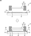
図1には、従来の固体撮像装置が示されている。図1Aは、固体撮像装置の平面図であり、図1Bは、固体撮像装置の側面図である。 FIG. 1 shows a conventional solid-state imaging device. 1A is a plan view of the solid-state imaging device, and FIG. 1B is a side view of the solid-state imaging device.
図1に示すように、固体撮像装置11は、光を受光する複数の画素が配置された撮像素子12の受光面を保護するため、撮像素子12の基板上に、露光プロセス、または定量吐出塗布、印刷等によりリブ13が形成され、リブ13にシールガラス14が搭載されて構成されている。撮像素子12の受光面とシールガラス14との間は、中空構造となっている。
As shown in FIG. 1, the solid-
ここで、例えば、特許文献1には、光硬化性接着剤(感光性接着剤)と熱硬化性接着剤との特性を利用して、半導体ウェハに蓋部を接着する技術が開示されている。また、特許文献2には、撮影レンズの光軸に垂直な面と、固体撮像装置の撮像面との平行度を高精度にする技術が開示されている。 Here, for example, Patent Document 1 discloses a technique for bonding a lid portion to a semiconductor wafer by using the characteristics of a photocurable adhesive (photosensitive adhesive) and a thermosetting adhesive. . Japanese Patent Application Laid-Open No. 2004-228561 discloses a technique for making the parallelism between a surface perpendicular to the optical axis of a photographing lens and an imaging surface of a solid-state imaging device highly accurate.
しかしながら、従来の固体撮像装置では、シールガラスを支持するリブが光硬化性接着剤を使用した露光プロセス等により形成されるため、例えば、数十μm程度しかリブ高さを確保することができず、撮像素子の受光面とシールガラスとの間隔を広く確保することは困難であった。このため、従来の固体撮像装置では、シールガラスが撮像素子の受光面に近接することになり、シールガラスのパーティクル(粉塵やキズなど)の影響を過大に受けることがあり、例えば、画像に影が発生することがあった。 However, in the conventional solid-state imaging device, since the rib supporting the seal glass is formed by an exposure process using a photo-curable adhesive, the height of the rib can only be secured, for example, about several tens of μm. It has been difficult to ensure a wide interval between the light receiving surface of the image sensor and the seal glass. For this reason, in the conventional solid-state imaging device, the seal glass is close to the light receiving surface of the image sensor, and may be excessively affected by particles (dust, scratches, etc.) of the seal glass. May occur.
本発明は、このような状況に鑑みてなされたものであり、パーティクルの影響を抑制することができるようにするものである。 The present invention has been made in view of such a situation, and makes it possible to suppress the influence of particles.
本発明の一側面の固体撮像装置は、受光面において光を受光する撮像素子と、前記撮像素子の受光面を覆う透光体および前記透光体の外周を固定する枠体を有し、前記撮像素子の受光面の周縁領域に装着される保護部品とを備え、少なくとも前記枠体が、モールド成形により成形されたものであり、前記保護部品の上端部が、その下端部となる前記枠体よりも外周方向に延長するように所定の幅を有して幅広に形成され、他の部品を装着可能な装着部とされる。 A solid-state imaging device according to one aspect of the present invention includes an imaging element that receives light on a light-receiving surface, a light-transmitting body that covers the light-receiving surface of the imaging element, and a frame that fixes an outer periphery of the light-transmitting body. and a protection component to be mounted on the peripheral area of the light receiving surface of the imaging device, at least the frame body state, and are not molded by molding, the upper end portion of the protective part, the frame serving as the lower end The mounting portion has a predetermined width so as to extend in the outer circumferential direction from the body, and is a mounting portion on which other components can be mounted .
本発明の一側面においては、受光面において光を受光する撮像素子の受光面の周縁領域に装着される保護部品が、撮像素子の受光面を覆う透光体と、その透光体の外周を固定する枠体とを有し、少なくとも枠体が、モールド成形により成形されている。そして、保護部品の上端部が、その下端部となる枠体よりも外周方向に延長するように所定の幅を有して幅広に形成され、他の部品を装着可能な装着部とされる。 In one aspect of the present invention, a protective component attached to the peripheral region of the light receiving surface of the image sensor that receives light on the light receiving surface includes a light transmitting body that covers the light receiving surface of the image sensor, and an outer periphery of the light transmitting body. A frame body to be fixed, and at least the frame body is formed by molding. Then, the upper end portion of the protective component is formed to be wider with a predetermined width so as to extend in the outer circumferential direction than the frame body serving as the lower end portion thereof, and is a mounting portion on which other components can be mounted.
本発明の一側面によれば、パーティクルの影響を抑制することができる。 According to one aspect of the present invention, the influence of particles can be suppressed.
以下、本発明を適用した具体的な実施の形態について、図面を参照しながら詳細に説明する。 Hereinafter, specific embodiments to which the present invention is applied will be described in detail with reference to the drawings.
図2には、本発明を適用した固体撮像装置の一実施の形態の構成例が示されている。図2Aは、固体撮像装置の平面図であり、図2Bは、固体撮像装置の側面図である。 FIG. 2 shows a configuration example of an embodiment of a solid-state imaging device to which the present invention is applied. FIG. 2A is a plan view of the solid-state imaging device, and FIG. 2B is a side view of the solid-state imaging device.
図2において、固体撮像装置21は、撮像素子22および保護部品23を備え、シールガラス24とモールド樹脂25とが一体成形された保護部品23が、撮像素子22上に直接的にマウントされて構成されている。
In FIG. 2, the solid-
CCDやCMOSセンサなどの撮像素子22の表面(図2Bの上側の面)の中央領域には、光を受光する複数の画素が配列され、光を受光する受光面が形成されており、その受光面には、それぞれの画素ごとにマイクロレンズ31が配設されている。また、撮像素子22の表面の周辺部には、画素から出力される電気信号を外部に出力するための複数の端子32が形成されている。
A plurality of pixels that receive light are arranged in the central region of the surface of the
保護部品23は、撮像素子22の受光部を保護するための部品であって、個片化された透光体であるシールガラス24と、シールガラス24の外周を固定する枠体でありモールド成形された樹脂からなるモールド樹脂25とが一体成形されて構成されている。また、モールド樹脂25としては、例えば、黒色の樹脂が使用され、モールド樹脂25は遮光性を備えている。
The
また、保護部品23は、接着剤33により撮像素子22の表面に接着される。
The
例えば、図3に示すように、接着剤33は、モールド樹脂25の底面の幅と同一の幅で、撮像素子22の受光面(マイクロレンズ31が配置されている領域)よりも外側の領域であって、複数の端子32よりも内側の領域である周縁領域に塗布される。接着剤33としては、例えば、エポキシ樹脂を含有する熱硬化型のものが使用され、接着剤33は、撮像素子22の表面の凹凸が隠れる程度の厚みで塗布される。なお、接着剤33としては、光硬化型の接着剤を使用してもよい。
For example, as shown in FIG. 3, the
そして、接着剤33の塗布面にモールド樹脂25を載置して、その後、接着剤33を硬化させる硬化処理(Cure)を行うことで、保護部品23が撮像素子22の表面に接着される。また、撮像素子22の表面の周辺部に形成されている複数の端子32には、撮像素子22の各画素から出力される電気信号を外部の装置に供給するためのワイヤ34が、それぞれワイヤボンディングされる。
Then, the
次に、図4のフローチャートを参照して、固体撮像装置21の製造プロセスを説明する。
Next, a manufacturing process of the solid-
ステップS11において、ガラス基板をダイシングしてシールガラス24を個片化するガラス加工工程が行われる。
In step S11, a glass processing step of dicing the glass substrate to separate the
例えば、図5Aに示すように、ガラス基板41の裏面に接着されたダイシングテープにより、ガラス基板41がフレーム42にテープマウントされる。そして、ダイヤモンド製の円形回転刃などからなるガラスダイサ43を高速回転させ、超純水で冷却しながらガラス基板41を切断する。その後、UV(紫外線)照射機により、紫外線を照射することによってダイシングテープを剥離し、シールガラス24が個片化される。
For example, as shown in FIG. 5A, the
また、ダイシング時のシールガラス24の側面は、ガラスの強度、モールド樹脂25の硬化による応力、撮像素子22に接着した後の応力、またはプロセス数などを考慮して、垂直に切削(フルカット)したり、片側または両側について面取り(べベルカット)をするなどの各種のカット方法が適宜選択される。また、面取りには、45度で切削するC面取りや、所定の曲率で切削するR面取りなどがある。
Further, the side surface of the
ステップS12において、シールガラス24を樹脂でモールド(射出成型)して保護部品23を成形するモールド成形工程が行われる。
In step S12, a molding process for molding the
例えば、図5Bに示すように、フレーム42上にあるダイシング済みのシールガラス24が、モールド樹脂25を成形するための金型44にセット(ガラスソート)される。その後、所定の温度に加温されて軟化した樹脂を金型44に射出して充填させ、シールガラス24の周囲を樹脂でモールドする。そして、金型44に流し込まれた樹脂が固化してモールド樹脂25となることで保護部品23が成形される。
For example, as shown in FIG. 5B, the
ステップS13において、撮像素子22の表面に接着剤33を塗布する接着剤塗布工程が行われる。
In step S <b> 13, an adhesive application process for applying the adhesive 33 to the surface of the
例えば、図5Cに示すように、撮像素子22の表面に接着剤33が塗布される。また、接着剤33を塗布する塗布方法には、液体の接着剤を精度良く定量供給するディスペンスや、凸版などを利用して接着剤を転写する印刷などの方法がある。また、ウェハの状態のままの撮像素子22に対して接着剤33を塗布したり、ウェハをダイシングして個片化された撮像素子22に接着剤33を塗布してもよい。
For example, as illustrated in FIG. 5C, the adhesive 33 is applied to the surface of the
ステップS14において、保護部品23を撮像素子22の表面に搭載するボンディング工程が行われる。
In step S <b> 14, a bonding process for mounting the
例えば、図5Dに示すように、金型44から取り出された保護部品23を、チップトレーガラスボンダ45により、撮像素子22の表面に保護部品23が正確に搭載される。また、撮像素子22に保護部品23を搭載する処理は、例えば、撮像素子22が載置されるステージ46の温度、または、保護部品23を運搬するチップトレーガラスボンダ45の温度を常温より高い温度とした環境で行うことができる。このように、ステージ46またはチップトレーガラスボンダ45の温度を常温より高くすることにより、保護部品23を撮像素子22の表面に載置することで、保護部品23を撮像素子22に仮固定することができる。なお、撮像素子22に保護部品23を搭載する処理を、常温の環境で行ってもよい。
For example, as shown in FIG. 5D, the
ステップS15において、接着剤33を硬化させる硬化処理(Cure)が行われる。 In step S15, a curing process (Cure) for curing the adhesive 33 is performed.
例えば、図5Eに示すように、複数の固体撮像装置21が、例えば、Cureオーブン内で加温されることで、接着剤33が硬化し、保護部品23が撮像素子22の表面に固定される。
For example, as shown in FIG. 5E, the plurality of solid-
ここで、硬化処理では、固体撮像装置21が高温の環境下に置かれることにより、撮像素子22の表面と保護部品23との間の空間内の圧力(キャビティ内の内圧)が上昇するため、撮像素子22から保護部品23が剥がれることが懸念される。このような内圧の上昇による悪影響を回避するため、加圧オーブンにより固体撮像装置21を加温することや、保護部品23を固定する固定ジグを使用すること、段階的に温度を上昇させるステップCureを行うことなどの対処を施すことができる。
Here, in the curing process, since the solid-
以上のように、シールガラス24の外周を固定するモールド樹脂25をモールド成形することにより、モールド樹脂25を任意の高さに設計することができ、撮像素子22の受光面とシールガラス24との間隔を、従来よりも広く確保することができる。これにより、シールガラス24のパーティクルの影響を抑制することができ、例えば、撮像素子22により撮像される画像に影が発生することなどが防止される。
As described above, by molding the
即ち、従来の固体撮像装置では、シールガラスが撮像素子の受光面に近接していたためにパーティクルの影響を過大に受けることがあったが、一般的に、撮像素子の受光面とシールガラスとの間隔を広くすることで、パーティクルの影響を回避することができる。従って、固体撮像装置21では、パーティクルの影響を回避することができる程度に、モールド樹脂25がシールガラス24を支持する高さを設計し、シールガラス24のパーティクルの影響を抑制することができる。
That is, in the conventional solid-state imaging device, the seal glass is close to the light receiving surface of the image sensor, and thus may be excessively affected by particles. By increasing the interval, the influence of particles can be avoided. Therefore, in the solid-
また、モールド樹脂25に黒色の樹脂を使用することで、モールド樹脂25に遮光性を備えることができ、これにより、撮像素子22の受光面に対して反射光または散乱光が側方から入射することを防止することができる。このように反射光または散乱光が側方から入射することを防止することで、撮像素子22により撮像された画像にフレアやゴーストなどが発生することを防止することができる。
In addition, by using a black resin for the
即ち、従来の固体撮像装置では、例えば、光硬化性接着剤を利用してシールガラスを撮像素子に固定しており、光硬化性接着剤は透光性が必要になるために遮光性を備えることは困難であり、硬化後の光硬化性接着剤を透過して側方から撮像素子に反射光または散乱光が入射することがあった。これに対し、固体撮像装置21では、シールガラス24を固定するモールド樹脂25をモールド成形により成形するので、黒色の樹脂を採用することで容易に遮光性を備えることができる。
That is, in a conventional solid-state imaging device, for example, a sealing glass is fixed to an imaging element using a photocurable adhesive, and the photocurable adhesive has light shielding properties because it needs translucency. This is difficult, and reflected light or scattered light may enter the image pickup device from the side through the cured photocurable adhesive. On the other hand, in the solid-
また、固体撮像装置21では、シールガラス24の周囲の上面および下面が、モールド樹脂25により挟み込むようにモールドされるので、シールガラス24がモールド樹脂25により補強されることになる。これにより、シールガラス24に歪を発生し難くすることができる。
Further, in the solid-
ここで、モールド樹脂25としては、エポキシ系の樹脂を材料とすることで、耐熱性などの硬化物物性に対する要求、および、不純物に対する耐腐食性などの信頼性に対する要求を満たすことができる。また、露光プロセスにより成形されるリブを使用した場合には、結露の問題や、フィラーなどの添加剤が受光面に悪影響を与える問題などがあるが、モールド成形されるモールド樹脂25を使用することにより、それらの問題が発生することを回避することができる。
Here, as the
また、シールガラス24としては、樹脂またはガラスで構成されるレンズなどの光学部品や、各種の光学フィルタ(IRCF(Infrared Cut Filter)、OLPF(Optical Low Pass Filer))などを使用することができ、これにより、それらの光学特性を有する固体撮像装置21を小型化することができる。
As the
また、固体撮像装置21は、例えば、他の部品を装着可能な装着部を有する保護部品を使用することができる。
Moreover, the solid-
即ち、図6は、固体撮像装置21に装着される保護部品の他の構成例を示す図である。
That is, FIG. 6 is a diagram illustrating another configuration example of the protective component attached to the solid-
図6に示すように、保護部品51のモールド樹脂52は、図3のモールド樹脂25と同様の幅で形成された枠体53と、枠体53よりも幅広に形成された装着部54とを有する。このように、装着部54が、枠体53よりも外周方向に延長するように所定の幅を有して形成されているので、モールド樹脂52は、シールガラス24の外周を固定するとともに、装着部54に他の部品を装着させることができる。
As shown in FIG. 6, the
例えば、モールド樹脂52は、図6に示すような断面形状の金型により成形してもよいし、装着部54を含む幅の枠体を形成した後に、その幅広の枠体の下方部分を外周側から枠体53の幅となるまで切削することにより成形してもよい。また、装着部54より幅の狭い枠体53を有することにより、図6の下側に示すように、撮像素子22の表面の周辺部に形成されている端子32にワイヤ34をボンディングするための空間を確保することができる。
For example, the
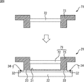
図7には、レンズ鏡筒62が装着された固体撮像装置21の側面図が示されている。
FIG. 7 shows a side view of the solid-
レンズ鏡筒62は、複数のレンズ61を収納しており、固体撮像装置21の表面に固定された保護部品51の装着部54の上面に、接着剤63により接着されて固定される。
The
このように、保護部品51が幅広の装着部54を備えることで、レンズ鏡筒62などの他の部品を、保護部品51を介して撮像素子22にマウントすることができる。
As described above, when the
また、モールド樹脂52は、モールド樹脂25と同様にモールド成形により成形されるので、例えば、露光プロセスで形成される樹脂リブよりも加工精度を向上させることができる。これにより、レンズ鏡筒62が装着される装着部54の上面の平行度を高精度に仕上げることができ、撮像素子22の受光面に対するレンズ鏡筒62の光軸の精度(アオリ精度)を高精度にすることができる。即ち、撮像素子22に対して正確にレンズ鏡筒62を位置決めすることができ、軸調整無でのレンズ鏡筒62の搭載を可能とする。
Further, since the
また、保護部品51に直接的にレンズ鏡筒62をマウントすることで、固体撮像装置21を小型化することができる。これにより、例えば、レンズ設計の外形規格の自由度が高くなり、バックフォーカスの距離設計の自由度を高くすることができる。
Further, by mounting the
なお、保護部品51を撮像素子22に接着する接着剤33は、撮像素子22の表面の凹凸が隠れる程度の厚みよりも厚く塗布されていてもよく、例えば、レンズ鏡筒62と撮像素子22の受光面との平行度を確保することができるような厚みであればよい。
Note that the adhesive 33 that adheres the
また、固体撮像装置21は、例えば、透明樹脂を使用して、いわゆる二色成形により一体化された保護部品を使用することができる。即ち、図3の保護部品23は、シールガラス24を固定するようにモールド樹脂25がモールド成型され、シールガラス24とモールド樹脂25とは独立した部品であるが、シールガラス24に替えて透明樹脂を使用することで、保護部品を一つの部品とすることができる。
Moreover, the solid-
即ち、図8は、固体撮像装置21に装着される保護部品のさらに他の構成例を示す図である。
That is, FIG. 8 is a diagram illustrating still another configuration example of the protective component attached to the solid-
図8の保護部品71は、透明樹脂により成型された透光体72と、透光体72の外周側に形成された枠部73とが、モールドプロセス時に一括で成形されて構成されている。例えば、保護部品71の金型に樹脂を流し込んでモールド成形する工程において、保護部品71の透光体72に該当する部分に透明樹脂を注入するとともに、枠部73に該当する部分に黒色樹脂を注入する。このとき、それぞれの樹脂の注入速度を適切にコントロールすることで、それぞれに該当する部分に透明樹脂と黒色樹脂が注入されて二色成形が行われる。
The
このように、透光体72と枠部73とを一括で成形することで、保護部品71の製造工程を、例えば、図3の保護部品23の製造工程よりも短縮することができ、これにより、コストダウンを図ることができる。
Thus, by forming the
なお、図3、図6、および図8に示した固体撮像装置21は、ワイヤボンディングにより外部の装置との接続が行われているが、例えば、貫通孔を利用して、裏面配線により外部の装置との接続が行われるような固体撮像装置に保護部品を装着してもよい。
Note that the solid-
即ち、図9は、固体撮像装置の他の構成例を示す図である。 That is, FIG. 9 is a diagram illustrating another configuration example of the solid-state imaging device.
図9の固体撮像装置81は、撮像素子22の各画素から出力される電気信号を外部の装置に供給するための配線82が、撮像素子22の表面(受光面が形成されている面)の反対側となる裏面に形成されている。そして、画素から出力される電気信号を外部に出力するための複数の端子32と、裏面の配線82とが貫通孔83を介して電気的に接続されている。
In the solid-
このように、裏面の配線82を有する固体撮像装置81に、図9Aに示すように、シールガラス24の外周がモールド樹脂25により固定された保護部品23(図3の保護部品23と同一)を装着することができる。また、図9Bに示すように、固体撮像装置81に、装着部54を有する保護部品51(図6の保護部品51と同一)を装着することができる。また、図9Cに示すように、固体撮像装置81に、透光体72と枠部73とがモールドプロセス時に一括で成形された保護部品71(図8の保護部品71と同一)を装着することができる。
9A, the protective component 23 (same as the
このように、裏面の配線82を有する固体撮像装置81に保護部品23,51、または71を装着する際、固体撮像装置81の上面においてワイヤをボンディングするための空間を確保する必要がなく、固体撮像装置81の受光面以外の上面の全てに保護部品23,51、または71が接触可能となり、それらの設計の自由度が向上する。また、図9Bに示すように、撮像素子22より広い装着部54を有する保護部品51を用いることで、固体撮像装置81より大きな部品を装着することができる。
Thus, when mounting the
なお、上述のフローチャートを参照して説明した各処理は、必ずしもフローチャートとして記載された順序に沿って時系列に処理する必要はなく、並列的あるいは個別に実行される処理(例えば、並列処理あるいはオブジェクトによる処理)も含むものである。 Note that the processes described with reference to the flowcharts described above do not necessarily have to be processed in chronological order in the order described in the flowcharts, but are performed in parallel or individually (for example, parallel processes or objects). Processing).
なお、本発明の実施の形態は、上述した実施の形態に限定されるものではなく、本発明の要旨を逸脱しない範囲において種々の変更が可能である。 The embodiment of the present invention is not limited to the above-described embodiment, and various modifications can be made without departing from the gist of the present invention.
21 固体撮像装置, 22 撮像素子, 23 保護部品, 24 シールガラス, 25 モールド樹脂, 31 マイクロレンズ, 32 端子, 33 接着剤, 34 ワイヤ, 41 ガラス基板, 42 フレーム, 43 ガラスダイサ, 44 金型, 45 チップトレーガラスボンダ, 46 ステージ, 51 保護部品, 52 モールド樹脂, 53 枠体, 54 装着部, 61 レンズ, 62 レンズ鏡筒, 63 接着剤, 71 保護部品, 72 透光体, 73 枠部, 81 固体撮像装置, 82 配線, 83 貫通孔 21 solid-state imaging device, 22 imaging device, 23 protective component, 24 sealing glass, 25 mold resin, 31 microlens, 32 terminal, 33 adhesive, 34 wire, 41 glass substrate, 42 frame, 43 glass dicer, 44 mold, 45 Chip tray glass bonder, 46 stages, 51 protective parts, 52 mold resin, 53 frame, 54 mounting part, 61 lens, 62 lens barrel, 63 adhesive, 71 protective part, 72 translucent body, 73 frame part, 81 Solid-state imaging device, 82 wiring, 83 through-hole
Claims (6)
前記撮像素子の受光面を覆う透光体および前記透光体の外周を固定する枠体を有し、前記撮像素子の受光面の周縁領域に装着される保護部品と
を備え、
少なくとも前記枠体が、モールド成形により成形されたものであり、
前記保護部品の上端部が、その下端部となる前記枠体よりも外周方向に延長するように所定の幅を有して幅広に形成され、他の部品を装着可能な装着部とされる
固体撮像装置。 An image sensor that receives light at the light receiving surface;
A light-transmitting body that covers the light-receiving surface of the image sensor and a frame that fixes the outer periphery of the light-transmitting body, and a protective component that is attached to a peripheral region of the light-receiving surface of the image sensor,
At least the frame body state, and are not molded by molding,
A solid part that has a predetermined width and is widened so that an upper end portion of the protective component extends in an outer peripheral direction from the frame body serving as a lower end portion thereof, and is a mounting portion on which other components can be mounted Imaging device.
請求項1に記載の固体撮像装置。 A lens barrel that houses the lens is mounted on the mounting portion of the protective component.
The solid-state imaging device according to claim 1 .
請求項1に記載の固体撮像装置。 The solid-state imaging device according to claim 1, wherein the frame of the protective component has a light shielding property.
請求項1に記載の固体撮像装置。 The solid-state imaging device according to claim 1, wherein the protective component is integrally formed by molding a mold resin that is the frame body on an outer periphery of a seal glass that is the light transmitting body.
請求項1に記載の固体撮像装置。 The solid-state imaging device according to claim 1, wherein a transparent resin is employed as the translucent body, and the transparent resin and the frame body are integrally molded by two-color molding.
請求項1に記載の固体撮像装置。The solid-state imaging device according to claim 1.
Priority Applications (2)
| Application Number | Priority Date | Filing Date | Title |
|---|---|---|---|
| JP2009217717A JP5487842B2 (en) | 2009-06-23 | 2009-09-18 | Solid-state imaging device |
| US12/789,099 US20100321563A1 (en) | 2009-06-23 | 2010-05-27 | Solid-state imaging unit |
Applications Claiming Priority (3)
| Application Number | Priority Date | Filing Date | Title |
|---|---|---|---|
| JP2009148797 | 2009-06-23 | ||
| JP2009148797 | 2009-06-23 | ||
| JP2009217717A JP5487842B2 (en) | 2009-06-23 | 2009-09-18 | Solid-state imaging device |
Publications (3)
| Publication Number | Publication Date |
|---|---|
| JP2011030173A JP2011030173A (en) | 2011-02-10 |
| JP2011030173A5 JP2011030173A5 (en) | 2012-10-18 |
| JP5487842B2 true JP5487842B2 (en) | 2014-05-14 |
Family
ID=43354020
Family Applications (1)
| Application Number | Title | Priority Date | Filing Date |
|---|---|---|---|
| JP2009217717A Expired - Fee Related JP5487842B2 (en) | 2009-06-23 | 2009-09-18 | Solid-state imaging device |
Country Status (2)
| Country | Link |
|---|---|
| US (1) | US20100321563A1 (en) |
| JP (1) | JP5487842B2 (en) |
Cited By (1)
| Publication number | Priority date | Publication date | Assignee | Title |
|---|---|---|---|---|
| FR3142039A1 (en) * | 2022-11-14 | 2024-05-17 | Stmicroelectronics International N.V. | Chip package and its manufacturing process |
Families Citing this family (5)
| Publication number | Priority date | Publication date | Assignee | Title |
|---|---|---|---|---|
| JP2014138119A (en) * | 2013-01-17 | 2014-07-28 | Sony Corp | Semiconductor device and semiconductor device manufacturing method |
| JP2015038920A (en) | 2013-08-19 | 2015-02-26 | ソニー株式会社 | Imaging apparatus and electronic apparatus |
| EP3226050A4 (en) * | 2014-11-27 | 2017-12-06 | Panasonic Intellectual Property Management Co., Ltd. | Imaging apparatus |
| WO2018145644A1 (en) | 2017-02-08 | 2018-08-16 | 宁波舜宇光电信息有限公司 | Camera module, moulded photosensitive component thereof, manufacturing method therefor, and electronic device |
| CN111034167B (en) * | 2017-08-29 | 2021-12-14 | 索尼半导体解决方案公司 | Image forming apparatus and method of manufacturing the same |
Family Cites Families (25)
| Publication number | Priority date | Publication date | Assignee | Title |
|---|---|---|---|---|
| US6795120B2 (en) * | 1996-05-17 | 2004-09-21 | Sony Corporation | Solid-state imaging apparatus and camera using the same |
| JPH1126782A (en) * | 1997-06-30 | 1999-01-29 | Olympus Optical Co Ltd | Semiconductor device |
| JP2002094035A (en) * | 2000-09-14 | 2002-03-29 | Shinko Electric Ind Co Ltd | Light-transmitting cap and its manufacturing method |
| DE10109787A1 (en) * | 2001-02-28 | 2002-10-02 | Infineon Technologies Ag | Digital camera with a light-sensitive sensor |
| JP4698874B2 (en) * | 2001-04-24 | 2011-06-08 | ローム株式会社 | Image sensor module and method of manufacturing image sensor module |
| JP4197228B2 (en) * | 2001-12-11 | 2008-12-17 | パナソニック株式会社 | Solid-state imaging device and manufacturing method thereof |
| US6876544B2 (en) * | 2003-07-16 | 2005-04-05 | Kingpak Technology Inc. | Image sensor module and method for manufacturing the same |
| JP4441211B2 (en) * | 2003-08-13 | 2010-03-31 | シチズン電子株式会社 | Small imaging module |
| JP2005109092A (en) * | 2003-09-30 | 2005-04-21 | Konica Minolta Opto Inc | Solid state imaging device and imaging apparatus having same |
| US20050117046A1 (en) * | 2003-12-02 | 2005-06-02 | Jichen Wu | Image sensor module and method for manufacturing the same |
| US7821564B2 (en) * | 2003-12-30 | 2010-10-26 | Given Imaging Ltd. | Assembly for aligning an optical system |
| US7872686B2 (en) * | 2004-02-20 | 2011-01-18 | Flextronics International Usa, Inc. | Integrated lens and chip assembly for a digital camera |
| JP3801601B2 (en) * | 2004-06-15 | 2006-07-26 | シャープ株式会社 | Manufacturing method of semiconductor wafer provided with lid and manufacturing method of semiconductor device |
| US20090040360A1 (en) * | 2006-02-24 | 2009-02-12 | Koji Taniguchi | Imaging device and portable terminal device |
| KR100817060B1 (en) * | 2006-09-22 | 2008-03-27 | 삼성전자주식회사 | Camera module and method of fabricating the same |
| JP2008197282A (en) * | 2007-02-09 | 2008-08-28 | Sharp Corp | Plastic lens unit, camera module and method for manufacturing them |
| WO2008132979A1 (en) * | 2007-04-17 | 2008-11-06 | Konica Minolta Opto, Inc. | Imaging device manufacturing method and imaging device |
| JP2008283002A (en) * | 2007-05-10 | 2008-11-20 | Sharp Corp | Imaging element module and its manufacturing method |
| JP2008289096A (en) * | 2007-05-21 | 2008-11-27 | Sharp Corp | Solid-state imaging module, imaging apparatus, imaging equipment, and method of manufacturing solid-state imaging module |
| EP2165225A4 (en) * | 2007-07-03 | 2012-05-09 | Optomecha Co Ltd | Lens unit composed of different materials and camera module and method for manufacturing the same |
| US8411192B2 (en) * | 2007-11-15 | 2013-04-02 | Sharp Kabushiki Kaisha | Image capturing module, method for manufacturing the image capturing module, and electronic information device |
| CN101630054A (en) * | 2008-07-15 | 2010-01-20 | 鸿富锦精密工业(深圳)有限公司 | Camera module and manufacturing method thereof |
| JP4694602B2 (en) * | 2008-09-02 | 2011-06-08 | シャープ株式会社 | Solid-state imaging device and electronic apparatus including the same |
| KR101032212B1 (en) * | 2009-09-14 | 2011-05-02 | 삼성전기주식회사 | Camera Module, focusing method of thereof and focusing device of thereof |
| JP2011180292A (en) * | 2010-02-26 | 2011-09-15 | Fujifilm Corp | Lens array |
-
2009
- 2009-09-18 JP JP2009217717A patent/JP5487842B2/en not_active Expired - Fee Related
-
2010
- 2010-05-27 US US12/789,099 patent/US20100321563A1/en not_active Abandoned
Cited By (1)
| Publication number | Priority date | Publication date | Assignee | Title |
|---|---|---|---|---|
| FR3142039A1 (en) * | 2022-11-14 | 2024-05-17 | Stmicroelectronics International N.V. | Chip package and its manufacturing process |
Also Published As
| Publication number | Publication date |
|---|---|
| JP2011030173A (en) | 2011-02-10 |
| US20100321563A1 (en) | 2010-12-23 |
Similar Documents
| Publication | Publication Date | Title |
|---|---|---|
| US7863062B2 (en) | Semiconductor device with a shielding section to prevent condensation and optical device module having the semiconductor device | |
| TWI305959B (en) | Optical device module, and method of fabricating the optical device module | |
| JP5487842B2 (en) | Solid-state imaging device | |
| KR100735446B1 (en) | Imaging device and its manufacturing method | |
| TWI711307B (en) | Optoelectronic modules including overmold supporting an optical assembly | |
| TWI386327B (en) | Bildaufnahmesystem und verfahren zu dessen herstellung | |
| US9525002B2 (en) | Image sensor device with sensing surface cavity and related methods | |
| JP2006005029A (en) | Imaging device and its manufacturing method | |
| JP4618639B2 (en) | Manufacturing method of semiconductor device | |
| JP2011035360A (en) | Method for manufacturing image pickup element package and structure thereof | |
| KR20080075880A (en) | Solid state imaging device and manufacturing method thereof | |
| JP2007142207A (en) | Solid-state image pickup device, and manufacturing method thereof | |
| US7999284B2 (en) | Semiconductor device and optical device module having the same | |
| JP2005317745A (en) | Solid-state imaging apparatus and method for manufacturing the same | |
| US20080296577A1 (en) | Camera module package | |
| JP5734769B2 (en) | Imaging lens and imaging module | |
| JP2017208468A (en) | Electronic component | |
| JP2007317719A (en) | Imaging device and its manufacturing method | |
| JP2011187482A (en) | Solid-state imaging apparatus, module for optical device, and method of manufacturing solid-state imaging apparatus | |
| US20120098080A1 (en) | Method and package for an electro-optical semiconductor device | |
| WO2016203923A1 (en) | Module, module manufacturing method, and electronic apparatus | |
| JP5694670B2 (en) | Solid-state imaging device and manufacturing method thereof | |
| JP2009123788A (en) | Solid-state imaging apparatus, method of manufacturing solid-state imaging apparatus, and photographic apparatus using the same solid-state imaging apparatus | |
| JP2006245118A (en) | Imaging device and its manufacturing method | |
| US10600835B2 (en) | Electronic module and method of manufacturing the same |
Legal Events
| Date | Code | Title | Description |
|---|---|---|---|
| A521 | Request for written amendment filed |
Free format text: JAPANESE INTERMEDIATE CODE: A523 Effective date: 20120904 |
|
| A621 | Written request for application examination |
Free format text: JAPANESE INTERMEDIATE CODE: A621 Effective date: 20120904 |
|
| A977 | Report on retrieval |
Free format text: JAPANESE INTERMEDIATE CODE: A971007 Effective date: 20130404 |
|
| A131 | Notification of reasons for refusal |
Free format text: JAPANESE INTERMEDIATE CODE: A131 Effective date: 20130409 |
|
| A521 | Request for written amendment filed |
Free format text: JAPANESE INTERMEDIATE CODE: A523 Effective date: 20130531 |
|
| TRDD | Decision of grant or rejection written | ||
| A01 | Written decision to grant a patent or to grant a registration (utility model) |
Free format text: JAPANESE INTERMEDIATE CODE: A01 Effective date: 20140128 |
|
| A61 | First payment of annual fees (during grant procedure) |
Free format text: JAPANESE INTERMEDIATE CODE: A61 Effective date: 20140210 |
|
| LAPS | Cancellation because of no payment of annual fees |