JP2009123788A - Solid-state imaging apparatus, method of manufacturing solid-state imaging apparatus, and photographic apparatus using the same solid-state imaging apparatus - Google Patents
Solid-state imaging apparatus, method of manufacturing solid-state imaging apparatus, and photographic apparatus using the same solid-state imaging apparatus Download PDFInfo
- Publication number
- JP2009123788A JP2009123788A JP2007293698A JP2007293698A JP2009123788A JP 2009123788 A JP2009123788 A JP 2009123788A JP 2007293698 A JP2007293698 A JP 2007293698A JP 2007293698 A JP2007293698 A JP 2007293698A JP 2009123788 A JP2009123788 A JP 2009123788A
- Authority
- JP
- Japan
- Prior art keywords
- solid
- state imaging
- imaging device
- lens
- optical element
- Prior art date
- Legal status (The legal status is an assumption and is not a legal conclusion. Google has not performed a legal analysis and makes no representation as to the accuracy of the status listed.)
- Pending
Links
Images


Abstract
Description
本発明は、受光素子が形成された固体撮像素子によって被写体の像を撮像する固体撮像装置、固体撮像装置の製造方法、及びその固体撮像装置を備えた撮影装置に関する。より詳細には、デジタルカメラやビデオカメラ等のカメラに用いられる固体撮像装置、固体撮像装置の製造方法、及びその固体撮像装置を備えた撮影装置に関するものである。 The present invention relates to a solid-state imaging device that captures an image of a subject using a solid-state imaging device on which a light-receiving element is formed, a method for manufacturing the solid-state imaging device, and an imaging device including the solid-state imaging device. More specifically, the present invention relates to a solid-state imaging device used for a camera such as a digital camera or a video camera, a manufacturing method of the solid-state imaging device, and an imaging device including the solid-state imaging device.
デジタルカメラやビデオカメラ等の撮影装置は、被写体からの光を電気信号に変換し、該電気信号に基づいて被写体の画像データを形成する。上記撮影装置には、撮像レンズによって結像された被写体からの光を認識する撮像部(固体撮像装置)が備えられている。 An imaging device such as a digital camera or a video camera converts light from a subject into an electrical signal, and forms image data of the subject based on the electrical signal. The imaging apparatus includes an imaging unit (solid-state imaging device) that recognizes light from a subject imaged by an imaging lens.
固体撮像装置によって認識された光は、固体撮像装置内部の固体撮像素子によって電気信号に変換され、該電気信号として出力される。そして、出力された電気信号に基づいて、上記撮影装置の処理部において被写体の画像が形成される。 The light recognized by the solid-state imaging device is converted into an electrical signal by a solid-state imaging device inside the solid-state imaging device and output as the electrical signal. Based on the output electrical signal, an image of the subject is formed in the processing unit of the photographing apparatus.
上述のような固体撮像装置の従来の構成としては、固体撮像素子が平行平面板状の保護ガラスを備えたユニットケース内に収められている構成を挙げることができる。上記保護ガラスは、光の入射を妨げずに、ユニットケースへの異物(塵や埃等)の侵入や固体撮像装置の製造工程における固体撮像素子への他の部材の接触を防ぐ。つまり、上記保護ガラスは、固体撮像素子に対する悪影響(異物の付着や物理的な原因による素子の破損)から固体撮像素子を保護する部材である。 As a conventional configuration of the solid-state imaging device as described above, a configuration in which the solid-state imaging device is housed in a unit case provided with a parallel flat plate-like protective glass can be exemplified. The protective glass prevents entry of foreign matter (dust, dust, etc.) into the unit case and contact of other members with the solid-state imaging device in the manufacturing process of the solid-state imaging device without preventing light from entering. In other words, the protective glass is a member that protects the solid-state image sensor from adverse effects on the solid-state image sensor (attachment of foreign matter or damage to the element due to physical causes).
上記構成を有する固体撮像装置を撮影装置に適用した場合における、固体撮像素子に入射する光の角度について、図10を用いて説明する。 An angle of light incident on the solid-state imaging device when the solid-state imaging device having the above-described configuration is applied to an imaging device will be described with reference to FIG.
図10に示すように、図示しない撮像レンズを透過した光は、保護ガラス101を介して固体撮像素子102に到達する。仮想線O−O’は、撮像レンズを透過した光の中心軸を表している。
As shown in FIG. 10, light that has passed through an imaging lens (not shown) reaches the solid-
固体撮像素子102に入射する光の内、仮想線O−O’から離れた位置に入射する光ほど仮想線O−O’から外側へ広がるような角度を有する。光が保護ガラス101内に入射する際、内側に屈折されるが、保護ガラス101から出射する際、保護ガラス101への入射光と平行な光として出射される。つまり、固体撮像素子102の外側に位置するほど、仮想線O−O’から外側に離れるような角度を有する光が、固体撮像素子102に入射する。
Of the light incident on the solid-
入射光が仮想線O−O’から外側に離れるような角度を有していると、固体撮像素子102への入射効率が低下するため、光を効率的に電気信号に変換することが困難になる。
If the incident light has an angle that leaves the imaginary line OO ′ to the outside, the incident efficiency to the solid-
上述のような平行平面板状の保護ガラスを備えた固体撮像装置を撮影装置に適用し、該固体撮像装置を小型化及び薄型化した場合、必然的に、撮像レンズを透過した光が広角化する。光の広角化によって、固体撮像素子の中心部と周辺部との間における入射効率の差がさらに拡大するため、形成された画像を閲覧すると周辺部が極端に暗くなってしまうという問題が生じる。 When a solid-state imaging device having a parallel flat plate-like protective glass as described above is applied to an imaging device, and the solid-state imaging device is reduced in size and thickness, the light transmitted through the imaging lens is inevitably widened. To do. Due to the widening of the light, the difference in incident efficiency between the central portion and the peripheral portion of the solid-state imaging device is further enlarged, and thus there arises a problem that the peripheral portion becomes extremely dark when the formed image is viewed.
固体撮像素子の保護部材として透明な平行平面板状の部材を用いた場合、上記問題の他に、以下のような問題が生じる。 When a transparent plane-parallel plate-like member is used as a protective member for a solid-state imaging device, the following problems occur in addition to the above problems.
固体撮像素子として多く用いられるCCD(charge coupled device:電荷結合素子)やCMOS(Complementary Metal Oxide Semiconductor)デバイスは、比較的広い波長の光を電気信号に変換することができる。例えば、CCDやC−MOSデバイスは、可視光領域のみならず近赤外領域(750〜2500nm)の波長を有する光を電気信号に変換することができる。 CCD (charge coupled device) and CMOS (Complementary Metal Oxide Semiconductor) devices, which are often used as solid-state imaging devices, can convert light having a relatively wide wavelength into electrical signals. For example, a CCD or C-MOS device can convert light having a wavelength in the near infrared region (750 to 2500 nm) as well as the visible light region into an electrical signal.
しかし、通常のカメラとして用いる場合、固体撮像素子が近赤外線を電気信号に変換することは、無意味であるだけでなく、解像度の低下や画像のムラ等画質の劣化を引き起こす。このため、通常、ビデオカメラ等の光学系に赤外カットフィルタとして色ガラス等を挿入することによって、入射光の内、近赤外線がカットされる。近年、装置の低コスト化及び小型化のために、赤外カットフィルタとして安価な誘電体多層膜を保護ガラスに形成することによって近赤外線をカット(反射)する方法が多く採用されている。 However, when used as a normal camera, it is not meaningless for the solid-state imaging device to convert near-infrared light into an electrical signal, but it also causes deterioration in image quality such as a decrease in resolution and image unevenness. For this reason, normally, near-infrared rays are cut out of incident light by inserting colored glass or the like as an infrared cut filter into an optical system such as a video camera. 2. Description of the Related Art In recent years, in order to reduce the cost and size of an apparatus, a method of cutting (reflecting) near infrared rays by forming an inexpensive dielectric multilayer film as an infrared cut filter on a protective glass has been adopted.
ここで、誘電体多層膜は、入射する光の角度によって反射する光の波長の範囲が変化する角度依存性を有している。光の入射角が大きくなるほど、誘電体多層膜が反射できる光の波長の範囲は、より短波長へシフトする。つまり、光の入射角が大きくなるほど、誘電体多層膜は、近赤外線が有する波長よりも短い波長を有する光を反射し易くなる。言い換えると、光の入射角が大きくなるほど、誘電体多層膜の赤外カットフィルタとしての機能が低下する。 Here, the dielectric multilayer film has an angle dependency in which the range of the wavelength of the reflected light changes depending on the angle of the incident light. As the incident angle of light increases, the wavelength range of light that can be reflected by the dielectric multilayer film shifts to a shorter wavelength. That is, the larger the incident angle of light, the more easily the dielectric multilayer film reflects light having a shorter wavelength than that of near infrared rays. In other words, the larger the incident angle of light, the lower the function of the dielectric multilayer film as an infrared cut filter.
このため、固体撮像素子によって変換された電気信号に基づいて形成された画像は、その中心部から周辺部へ向かうに伴って青みが強くなる。よって、解像度の低下や画像のムラ等画質の劣化を十分に防止することができなくなる。 For this reason, the image formed based on the electrical signal converted by the solid-state imaging device becomes bluish as it goes from the center to the periphery. Accordingly, it is impossible to sufficiently prevent deterioration in image quality such as a decrease in resolution and image unevenness.
上述のような画像の周辺部における画質の劣化という問題を解決するために、保護ガラスの上部にレンズを形成した撮像素子ユニット(固体撮像装置)が特許文献1に開示されている。また、特許文献2には、樹脂製集束レンズを有する誘電体多層膜フィルタの製造方法及び固体撮像デバイス(固体撮像装置)が開示されている。
In order to solve the above-described problem of deterioration in image quality in the peripheral portion of an image, an image sensor unit (solid-state imaging device) in which a lens is formed on the upper part of a protective glass is disclosed in Patent Document 1.
特許文献1の固体撮像装置について図11を用いて説明すると共に、特許文献2の固体撮像装置及び誘電体多層膜フィルタの製造方法について図12及び図13を用いて説明する。
The solid-state imaging device disclosed in Patent Document 1 will be described with reference to FIG. 11 and the solid-state imaging device disclosed in
図11に示すように、特許文献1の固体撮像装置は、ユニットケース112、ユニットケース112内に配置されたセンサチップ114、センサチップ114上に形成されたレンズ部116、及びセンサチップ114を保護する保護ガラス115を備えている。上記固体撮像装置の光の入射面側には、水晶の複屈折によって光線を2つに分光するための水晶フィルタ111及び被写体からの光を結像するための撮像レンズ110が備えられている。仮想線Oは、撮像レンズ110から入射する光の中心軸を表している。
As illustrated in FIG. 11, the solid-state imaging device disclosed in Patent Document 1 protects the
ここで、レンズ部116は、センサチップ114を構成する複数の受光画素のそれぞれ1つに対して形成された1つのマイクロレンズ116aから構成されている。保護ガラス115は、平板状のガラス板115a及びレンズ部115bから構成されており、ガラス板115a及びレンズ部115bは、一体形成されている。レンズ部115bは、ガラス板115aにおける光の入射面側に形成されている。保護ガラス115に形成されたレンズ部115bは、結像作用を有していないアフォーカル系のレンズ機能を有している。
Here, the
特許文献1の固体撮像装置は、レンズ部115bを備えているので、センサチップ114の周辺部に入射する光を、仮想線Oとほぼ平行になるように屈折させる。したがって、センサチップ114の周辺部における光の入射効率の低下を抑制し、得られる画像全体の均一性を達成し得る。
Since the solid-state imaging device of Patent Document 1 includes the
また、図12に示すように、特許文献2の固体撮像装置130は、ユニットケース136、ユニットケース136内に配置されたセンサチップ135、及びセンサチップ135の上部に形成された誘電体多層膜フィルタ131を備えている。誘電体多層膜フィルタ131は、センサチップ135を保護する光透過性基板134、光透過性基板134の平坦面に形成された誘電体多層膜133及び樹脂製集束レンズ132から構成されている。
As shown in FIG. 12, the solid-
固体撮像装置130の光の入射面側には、被写体からの光を結像するための光学系140が備えられている。矢印L0は、センサチップ135の中心部に入射する光の経路を示しており、矢印L2は、センサチップ135の外周付近に入射する光の経路を示している。
An
矢印L2上を進む光は、樹脂製集束レンズ132の光の入射面において、矢印L0とより平行になるように屈折する。したがって、樹脂製集束レンズ132から出射し、誘電体多層膜133に入射する光は、樹脂製集束レンズ132への入射前と比較して矢印L0を進む光と平行に近くなる。つまり、固体撮像装置130の外周付近に入射する光であっても、樹脂製集束レンズ132が設けられているので、比較的垂直な角度で誘電体多層膜133に入射させることができる。
The light traveling on the arrow L2 is refracted so as to be more parallel to the arrow L0 on the light incident surface of the
このため、固体撮像装置130は、その外周付近に入射する光の角度を適切に補正することによって、不要な赤外線をカットすることができる。この結果、画像全体の解像度の低下や色ムラを防止することができる。
For this reason, the solid-
さらに、図13に示すように、上記図12に示す特許文献2の誘電体多層膜フィルタの製造方法は、以下S101〜S105のような製造プロセスからなる。
Furthermore, as shown in FIG. 13, the method for manufacturing the dielectric multilayer filter of
図13に示すように、まず、大面積の光透過性基板134及び凸面成形型137を準備する(S101)。上記大面積の光透過性基板134の一面には、予め誘電体多層膜133が形成されている。また、凸面成形型137は、樹脂製集束レンズ132の凸面を転写するための凹型キャビティ137a及び平坦な形成面137bを有している。
As shown in FIG. 13, first, a large-area light-transmitting
次いで、大面積の光透過性基板134と凸面成形型137とを重ね合わせる。このとき、光硬化性樹脂138は、光透過性基板134と凸面成形型137とを重ね合わせる前及び後のいずれかの状態で充填される。そして、光透過性基板134側から紫外線を照射することによって、光硬化性樹脂138を硬化させる(S102)。
Next, the large area light
次いで、紫外線照射後の光透過性基板134から凸面成形型137を分離する(S103)。これによって、複数の樹脂製集束レンズ132が形成された光透過性基板134(形成体)を作製することができる。
Next, the
次いで、切断線139に沿って、複数の樹脂製集束レンズ132が形成された誘電体多層膜フィルタ131を切断する(S104)。この結果、複数の誘電体多層膜フィルタ131を製造することができる(S105)。
Next, the
以上のように、特許文献2の誘電体多層膜フィルタの製造方法を採用すれば、光の入射位置に関わらず効率的に近赤外線をカットし得る複数の誘電体多層膜フィルタ131を、1度の製造工程で簡便に製造することができる。さらに、レンズが光硬化性樹脂から構成されているため、ガラスを用いてレンズを形成した場合とは異なり、レンズ表面を所望の形状に成形することが容易である。
As described above, if the dielectric multilayer filter manufacturing method of
ここで、カメラ付き携帯電話やPDA(Personal Digital Assistant)等に搭載するためのカメラモジュールは、製品自体の小型化及び薄型化を達成するために、小型化及び薄型化の要求が高まっている。 Here, a camera module to be mounted on a camera-equipped mobile phone, a PDA (Personal Digital Assistant), or the like is increasingly required to be reduced in size and thickness in order to achieve reduction in size and thickness of the product itself.
しかし、図11及び図12に示した固体撮像装置において、固体撮像素子を保護するための部材(保護ガラス115及び誘電体多層膜フィルタ131)を、固体撮像素子の平面寸法(サイズ)より大きく形成せざるを得ない。この理由を以下に説明する。
However, in the solid-state imaging device shown in FIGS. 11 and 12, the members (
撮影装置を用いて被写体の像を撮影するためには、固体撮像素子によって被写体からの光が変換された電気信号を、固体撮像装置の外部にある処理部へ該電気信号を出力する必要がある。当然、電気信号の出力には配線が必要である。この配線として、通常、ボンディングワイヤによって固体撮像素子と処理部とを接続する。このボンディングワイヤが固体撮像素子の外側に張り出すように接続することから、ユニットケースを固体撮像素子よりも十分大きく形成する必要がある。結果として、保護ガラス115及び誘電体多層膜フィルタ131を大きくせざるを得ないので、上述のような固体撮像装置及び固体撮像装置は小型化に不向きな構造を有している。
In order to capture an image of a subject using an imaging device, it is necessary to output an electrical signal obtained by converting light from the subject by a solid-state imaging device to a processing unit outside the solid-state imaging device. . Naturally, wiring is necessary for outputting electric signals. As this wiring, the solid-state imaging device and the processing unit are usually connected by a bonding wire. Since the bonding wires are connected so as to protrude outside the solid-state image sensor, the unit case needs to be formed sufficiently larger than the solid-state image sensor. As a result, since the
さらに、ボンディングワイヤを保護ガラス115及び誘電体多層膜フィルタ131等と接触させないためには、ユニットケースを十分高く形成する必要があるので、上述のような固体撮像装置は薄型化することも困難である。
Furthermore, in order to prevent the bonding wire from contacting the
ここで、小型化及び薄型化が容易な撮影装置が特許文献3に開示されている。特許文献3の撮影装置の構造について、図14を用いて以下に説明する。
Here,
図14に示すように、特許文献3の撮影装置150は、両面に複数の導体配線161が形成された配線基板152、この配線基板152上に形成された画像処理用のDSP(Digital Signal Processor)154、スペーサ153を介してDSP154と接着された固体撮像装置151、配線基板152の一部や固体撮像装置151の側面を封止する封止樹脂158、この封止樹脂158上に固定されたレンズ保持具163、及び固体撮像装置151と対向して配置され、かつ固体撮像装置151への光路を画定する光路画定器として機能するレンズ162を備えている。センサチップ156及びDSP154と配線基板152とは、ボンディングワイヤ159とを介して電気的に接続されている。
As shown in FIG. 14, the
固体撮像装置151は、センサチップ156、及びセンサチップ156の有効画素領域と対向するように配置された光透過性基板155、及びセンサチップ156と光透過性基板155とを接着する接着部157から構成されている。配線基板152とセンサチップ156とを電気的に接続するためのボンディングワイヤ159が、接着部157の外側に接続されている。さらに、センサチップ156上にある有効画素領域に沿って接着部157が配置されている。また、センサチップ156の平面寸法より小さい平面寸法の光透過性基板155とセンサチップ156とが、接着部157を介して接着されている。
The solid-
平面寸法の小さい光透過性基板155を用いてセンサチップ156上にある有効画素領域を封止することができるため、光透過性基板155が、配線したボンディングワイヤ159に干渉されない。したがって、センサチップ156の近傍に光透過性基板155を配置し得る。
Since the effective pixel region on the
つまり、ボンディングワイヤ159と他の部材との接触を回避するための空間が不要になる。上記空間を設ける必要がなくなった分だけ、固体撮像装置151の小型化及び薄型化が可能である。結果として、撮影装置全体の小型化及び薄型化が容易である。
しかしながら、上記従来の特許文献1及び特許文献2の固体撮像装置を撮影装置に適用した場合、以下のような問題が生じる。
However, when the conventional solid-state imaging devices of Patent Literature 1 and
すなわち、特許文献1及び特許文献2の固体撮像装置において、レンズが形成された保護部材(保護ガラス115又は誘電体多層膜フィルタ131)は、ユニットケースを覆っている。上記保護部材を固体撮像素子と平行になるように取り付けなければ、固体撮像素子に入射する光束の中心軸と上記レンズの中心軸とが一致せず、大きな角度を有する(傾いた)状態になる。2つの中心軸間の角度ずれは固体撮像素子に入射する光の収差を拡大させるため、形成された画像の歪みやぼやけの原因になる。
That is, in the solid-state imaging devices of Patent Literature 1 and
上記保護部材を正確に取り付けるには、ユニットケースの形状が高精度に形成されていることが重要であるが、ユニットケースの形状を高精度化するには、製造工程におけるコストアップを避けることができない。 In order to attach the protective member accurately, it is important that the shape of the unit case is formed with high accuracy. However, to increase the shape of the unit case with high accuracy, it is necessary to avoid an increase in cost in the manufacturing process. Can not.
また、特許文献2の誘電体多層膜フィルタ131の製造方法においては、光透過性基板134の一面又は両面に誘電体多層膜133を形成した後、樹脂製集束レンズ132を形成することが記載されている。
In addition, in the manufacturing method of the
通常、誘電体多層膜133は40層〜50層の多層膜から構成されているため、光透過性基板134の一面のみに誘電体多層膜133を形成した場合、誘電体多層膜133の膜応力によって光透過性基板134に反りが生じる。反りが生じたままの光透過性基板134上に樹脂製集束レンズを形成すると、光透過性基板134の反りが樹脂製集束レンズに伝わり、特に樹脂製集束レンズの周辺部が変形する。樹脂製集束レンズが変形すると、光の入射角を適切に補正することができなくなるので、樹脂製集束レンズの変形は製品の良品率を大きく低下させる。
Usually, the
例えば、樹脂製集束レンズの形成前に、誘電体多層膜133を形成した光透過性基板134をダイシングによって小片化すれば、上記膜応力を開放(無視できる程度にまで軽減)することができる。しかし、先にダイシングを行うと、製造工程の簡略化及び低コスト化を実現することができなくなる。
For example, if the
また、光透過性基板134の両面に誘電体多層膜133を形成した場合、両面に形成された誘電体多層膜133の膜応力が互いに打ち消しあってくれるので、樹脂製集束レンズの形成後にダイシングを行ってもよい。しかし、光透過性基板134の、固体撮像素子であるセンサチップ135と対向する面に誘電体多層膜133を形成すると、以下のような問題が生じる。
In addition, when the
誘電体多層膜133は、赤外線を反射する機能には影響しない程度のひび割れを無数に有している。誘電体多層膜133は温度変化に影響を受け易いので、製造工程や実装後における装置の駆動によって生じる温度変化に伴って、上記ひび割れが拡大する可能性がある。ひび割れの拡大(複数のひび割れが繋がること)によって、赤外線を反射する機能には殆ど影響しない程度の膜の微小剥離が生じる。誘電体多層膜133の微小剥離を起こした小片が有効画素領域上に付着すると、画像にしみを形成してしまう。
The
すなわち、光透過性基板134の両面に誘電体多層膜133を形成した場合、固体撮像装置の良品率及び長期的な信頼性が低下する。さらに、光透過性基板134の両面に誘電体多層膜133を形成すると、当然のことながら、固体撮像装置の小型化及び薄型化の妨げになる。
That is, when the
ここで、特許文献3の固体撮像装置151(図14参照)に特許文献1又は特許文献2に記載の技術を適用すると、ユニットケース作製による作業の煩雑さやコストアップ、及び誘電体多層膜の微小剥離を解決すると同時に、固体撮像装置の小型化及び薄型化を達成し得る。
Here, when the technique described in Patent Document 1 or
すなわち、特許文献1及び特許文献2の問題は、以下の(1)〜(3)の理由によって解決し得る。
(1)光透過性基板を有効画素領域のサイズよりも若干大きくするだけでよいので、ボンディングワイヤと他の部材との接触を回避するための空間が不要になる。
(2)上面にレンズが形成された光透過性基板と固体撮像素子とが非常に薄い接着部を介して固定されているので、入射光の中心軸とレンズの中心軸とが大きく傾くことがない。
(3)小片化された光透過性基板を用いているので、誘電体多層膜の膜応力によるレンズの変形が起こらない。
That is, the problems of Patent Document 1 and
(1) Since the light-transmitting substrate only needs to be slightly larger than the size of the effective pixel region, a space for avoiding contact between the bonding wire and another member becomes unnecessary.
(2) Since the light-transmitting substrate on which the lens is formed on the upper surface and the solid-state imaging device are fixed through a very thin adhesive portion, the central axis of the incident light and the central axis of the lens may be greatly inclined. Absent.
(3) Since a small light-transmitting substrate is used, the lens is not deformed by the film stress of the dielectric multilayer film.
ここで、特許文献3の固体撮像装置151(図14参照)に特許文献1又は特許文献2に記載の技術を適用することを考えると、図15(a)に示す固体撮像装置151’を有する撮影装置150’となる。
Here, considering that the technique described in Patent Literature 1 or
すなわち、図15(a)に示すように、固体撮像装置151’は、光透過性基板155を覆う樹脂製レンズ155aを備えている。
That is, as shown in FIG. 15A, the solid-
上記樹脂製レンズ155aは、光透過性基板155と同じ表面形状を有しており、センサチップ156の有効画素領域と殆ど同じ表面形状を有している。樹脂製レンズ155a及び光透過性基板155の側壁は、平らな面を形成している。樹脂製レンズ155a及び光透過性基板155の側壁が平らな面を形成しているのは、樹脂製レンズ155a及び光透過性基板155が、ダイシングによって個片化されているためである。
The
この構成により、固体撮像装置151’は、製造コストの削減、及び光透過性基板155の反りの抑制を達成し得る。
With this configuration, the solid-
しかしながら、樹脂製レンズ155aの端部が平坦な側壁を有しているため、該側壁において光が反射され、上記有効画素領域上に迷光として入射する。すなわち、図15(b)に示すように、樹脂製レンズ155aの端部付近に入射する光170は、樹脂製レンズ155aの凸面において屈折された屈折光170aとして樹脂製レンズ155aに入射する。ここで、樹脂製レンズ155aの端部付近は、製造上、上記有効画素領域の真上からわずかに外側へはみ出している。このため、屈折光170aは、樹脂製レンズ155aの端部の上記側壁及び封止樹脂148から露出した光透過性基板155の側壁において反射した反射光170bになる。この反射光170bは、上記有効画素領域上に画像の形成に不要な光として入射する。この結果、固体撮像装置151’を用いて形成された画像の画質が低下するという問題点を有している。
However, since the end portion of the
ここで、上述のように、固体撮像装置151’において、封止樹脂158から光透過性基板155の側壁の一部が露出している。これは、封止樹脂158が光透過性基板155の上面に浸入しないようにするためである。
Here, as described above, in the solid-
センサチップ156及び光透過性基板155等を樹脂封止する際、過剰量の流動性を有する封止樹脂158を充填すると、光透過性基板155の上面に封止樹脂158が浸入し易くなる。したがって、流動性を有する封止樹脂158は、センサチップ156及び光透過性基板155等の封止に必要な量よりも少なめに充填される。
When the
この結果、封止樹脂158から光透過性基板155の側壁の一部が露出する。通常、光透過性基板155の側壁の内、光透過性基板155の上面から高さ50〜100μm程度の部分が、封止樹脂158から露出している。
As a result, a part of the side wall of the
以上のように、特許文献3の固体撮像装置151に樹脂製レンズ155aを形成すると、光透過性基板155の側壁及び樹脂製レンズ155aの端部の側壁における光の反射に伴い、有効画素領域へ入射する迷光が増加する。特に、封止樹脂158を備えてない固体撮像装置においては、光透過性基板155の側壁の全面が光の反射面として機能するので、有効画素領域へ入射する迷光がさらに増加する。
As described above, when the
本発明は、上記従来の問題点に鑑みなされたものであって、その目的は、固体撮像素子の周辺部への入射光が暗くなることを抑制し、かつ固体撮像素子の有効画素領域へ入射する迷光を抑制し、さらに、高い信頼性を得ることができる固体撮像装置、固体撮像装置の製造方法、及びその固体撮像装置を備えた撮影装置を提供することにある。 The present invention has been made in view of the above-described conventional problems, and an object thereof is to suppress the incident light to the peripheral part of the solid-state image sensor from becoming dark and to enter the effective pixel region of the solid-state image sensor. An object of the present invention is to provide a solid-state imaging device capable of suppressing stray light to be generated and obtaining high reliability, a method for manufacturing the solid-state imaging device, and an imaging device including the solid-state imaging device.
本発明の固体撮像装置は、上記課題を解決するために、有効画素領域が形成された固体撮像素子と、上記固体撮像素子の有効画素領域と対向するように配置された透明板と、上記固体撮像素子の一部、及び上記透明板の側壁を封止する封止樹脂と、透明な樹脂から構成された光学素子とを備え、上記光学素子は、上記透明板上に形成され、かつ該光学素子の光軸方向から見たときに、該光学素子の外周は該透明板の外周よりも光軸中心側に形成されていることを特徴としている。 In order to solve the above problems, a solid-state imaging device of the present invention includes a solid-state imaging device in which an effective pixel region is formed, a transparent plate disposed to face the effective pixel region of the solid-state imaging device, and the solid A sealing resin for sealing a part of the image sensor and the side wall of the transparent plate, and an optical element made of a transparent resin, the optical element being formed on the transparent plate, and the optical element When viewed from the optical axis direction of the element, the outer periphery of the optical element is formed closer to the optical axis center side than the outer periphery of the transparent plate.
本発明の固体撮像装置の製造方法は、上記課題を解決するために、固体撮像素子の有効画素領域と対向するように、かつ該固体撮像素子の平面形状の内側に存在するように透明板を配設する第1の工程と、上記固体撮像素子の一部、及び上記透明板の側壁を封止樹脂により封止する第2の工程と、上記透明板上に透明な樹脂から構成された光学素子を形成する第3の工程とを含み、上記第3の工程において上記光学素子と上記封止樹脂とは接しないことを特徴としている。 In order to solve the above-described problem, a method for manufacturing a solid-state imaging device according to the present invention provides a transparent plate so as to face the effective pixel region of the solid-state imaging device and to exist inside the planar shape of the solid-state imaging device. A first step of disposing, a second step of sealing a part of the solid-state imaging device, and a side wall of the transparent plate with a sealing resin, and an optical unit made of a transparent resin on the transparent plate And a third step of forming an element, wherein the optical element and the sealing resin are not in contact with each other in the third step.
上記の発明によれば、光学素子は、透明板上に形成され、かつ該光学素子の光軸方向から見たときに、該光学素子の外周は該透明板の外周よりも光軸中心側に形成されている。 According to the above invention, the optical element is formed on the transparent plate, and when viewed from the optical axis direction of the optical element, the outer periphery of the optical element is closer to the optical axis center side than the outer periphery of the transparent plate. Is formed.
したがって、光学素子が透明板上に形成されているので、固体撮像素子の周辺部への入射光が暗くなることを抑制することができる。 Therefore, since the optical element is formed on the transparent plate, it is possible to suppress the incident light to the peripheral part of the solid-state imaging element from becoming dark.
また、光学素子は、透明板と同じ外周の側壁を有していないので、固体撮像素子の有効画素領域へ入射する迷光を抑制することができる。 Moreover, since the optical element does not have the same outer peripheral side wall as the transparent plate, stray light incident on the effective pixel region of the solid-state imaging element can be suppressed.
また、例えば、光学素子を流動体の樹脂にて硬化させて形成する場合、光学素子成形時には、成形型に該樹脂を充填し、成形型と透明板とを接触させて硬化させる。その際、本発明では、光学素子は透明板上に形成され、封止樹脂上には形成されない。したがって、透明板上面と封止樹脂上面との段差部に樹脂が接触するということがなく、これによって、該段差から樹脂が漏れ出して所望の光学素子形状を得ることができないということがない。 For example, when the optical element is formed by curing with a fluid resin, when molding the optical element, the mold is filled with the resin, and the mold and the transparent plate are brought into contact with each other and cured. In that case, in this invention, an optical element is formed on a transparent plate, and is not formed on sealing resin. Therefore, the resin does not come into contact with the step portion between the upper surface of the transparent plate and the upper surface of the sealing resin, thereby preventing the resin from leaking out from the step and obtaining a desired optical element shape.
さらに、樹脂は、成形型と透明板とで密閉され大気に触れることがない。これにより、例えば、酸素による硬化阻害が起きる樹脂を選択することができ、自由度のある設計を行うことができる。この結果、信頼性のある高性能な固体撮像装置の製造方法を提供することができる。 Furthermore, the resin is sealed between the mold and the transparent plate and is not exposed to the atmosphere. Thereby, for example, a resin that inhibits curing by oxygen can be selected, and a design with flexibility can be performed. As a result, it is possible to provide a method for manufacturing a reliable and high-performance solid-state imaging device.
また、封止樹脂と光学素子とが接しないことにより、光学素子が封止樹脂から剥がることがない点において、高い信頼性及び耐環境性能を持った固体撮像装置とすることができる。 In addition, since the sealing resin and the optical element are not in contact, the solid-state imaging device having high reliability and environmental resistance can be obtained in that the optical element is not peeled off from the sealing resin.
したがって、固体撮像素子の周辺部への入射光が暗くなることを抑制し、かつ固体撮像素子の有効画素領域へ入射する迷光を抑制し、さらに、高い信頼性を得ることができる固体撮像装置、及び固体撮像装置の製造方法を提供することができる。 Therefore, it is possible to suppress the incident light to the peripheral portion of the solid-state imaging element from becoming dark, to suppress stray light that enters the effective pixel region of the solid-state imaging element, and to obtain high reliability, In addition, a method for manufacturing a solid-state imaging device can be provided.
本発明の固体撮像装置では、前記光学素子は、該光学素子の光軸方向から見たときに、該光学素子の外周が前記固体撮像素子の有効画素領域の外側になるように形成されていることが好ましい。 In the solid-state imaging device of the present invention, the optical element is formed so that the outer periphery of the optical element is outside the effective pixel region of the solid-state imaging element when viewed from the optical axis direction of the optical element. It is preferable.
これにより、光学素子は、固体撮像素子の有効画素領域の全面を覆っている。この結果、光学素子においても、上記有効画素領域の対応平面領域の外周部に入射した光を屈折させて、光の角度が直角に近づくように補正することができる。したがって、固体撮像素子の周辺部への入射光が暗くなることを確実に抑制することができる。 Thus, the optical element covers the entire effective pixel region of the solid-state image sensor. As a result, also in the optical element, it is possible to refract the light incident on the outer peripheral portion of the corresponding planar region of the effective pixel region and correct the light angle so as to approach a right angle. Accordingly, it is possible to reliably suppress the incident light to the peripheral portion of the solid-state imaging element from becoming dark.
また、本発明の固体撮像装置では、前記透明板は、前記固体撮像素子の平面形状の内側に存在するように配設されていることが好ましい。 In the solid-state imaging device of the present invention, it is preferable that the transparent plate is disposed so as to exist inside a planar shape of the solid-state imaging element.
これにより、透明板の面積を固体撮像素子の面積よりも小さくすることによって、固体撮像装置もそれに応じて小さくなり、結果的に、この固体撮像装置を備える撮像装置も小型のものを提供することができる。 Thereby, by making the area of the transparent plate smaller than the area of the solid-state imaging device, the solid-state imaging device is also reduced accordingly, and as a result, the imaging device including this solid-state imaging device is also provided with a small size Can do.
また、本発明の固体撮像装置では、前記光学素子は、該光学素子の光軸方向から見たときに、該光学素子の外周が曲線で形成されているとすることができる。 In the solid-state imaging device of the present invention, the optical element may be formed such that the outer periphery of the optical element is curved when viewed from the optical axis direction of the optical element.
これにより、例えば、光学素子を流動体の樹脂にて硬化させて形成する場合、光学素子の形成時に使用する成形型の内形は、急激な変曲点が存在せず連続しているため、切削時に欠けが生じ難く、容易に作製が可能である。したがって、成形型の作製において、低コストを図り得る固体撮像装置を提供することができる。 Thereby, for example, when the optical element is formed by curing with a fluid resin, the inner shape of the mold used when forming the optical element is continuous without a sharp inflection point, Chipping is unlikely to occur during cutting and can be easily manufactured. Therefore, it is possible to provide a solid-state imaging device that can achieve low cost in the production of the mold.
また、本発明の固体撮像装置では、前記光学素子は、該光学素子の光軸方向から見たときに、該光学素子の外周が1つ以上の直線を含んで形成されているとすることができる。 In the solid-state imaging device of the present invention, the optical element may be formed so that an outer periphery of the optical element includes one or more straight lines when viewed from the optical axis direction of the optical element. it can.
これにより、光学素子の外周として曲線よりも直線を用いることによって、光学素子中心の認識が容易となり、光学素子の形成時及び検査時に、撮像装置との位置調整用のマーカーとして機能することが可能となり、短時間で高精度な位置調整を行った低コスト、かつ高性能の固体撮像装置を提供することができる。 This makes it easy to recognize the center of the optical element by using a straight line rather than a curve as the outer periphery of the optical element, and can function as a marker for position adjustment with the imaging device when forming and inspecting the optical element. Thus, it is possible to provide a low-cost and high-performance solid-state imaging device that performs high-precision position adjustment in a short time.
また、本発明の固体撮像装置では、前記光学素子は、該光学素子の光軸方向から見たときに、該光学素子の外周が曲線と1つ以上の直線とで形成されているとすることができる。 In the solid-state imaging device of the present invention, the optical element has an outer periphery formed of a curved line and one or more straight lines when viewed from the optical axis direction of the optical element. Can do.
これにより、一般的に長方形である固体撮像素子の有効画素領域と、その有効画素領域よりも少し広めの長方形である透明板との間に、光学素子の外形を形成することができる。したがって、固体撮像素子の有効画素領域と同等程度の大きさの透明板を採用することができ、小型の固体撮像装置を提供することができる。 As a result, the outer shape of the optical element can be formed between the effective pixel region of the solid-state imaging device that is generally rectangular and the transparent plate that is a rectangle slightly wider than the effective pixel region. Therefore, a transparent plate having a size comparable to the effective pixel area of the solid-state image sensor can be employed, and a small solid-state image sensor can be provided.
また、本発明の固体撮像装置では、前記光学素子は、前記固体撮像素子の有効画素領域内に形成された有効領域と、それ以外の非有効領域とからなり、上記光学素子の有効領域は、撮像系における有効光束を屈折させて上記固体撮像素子の有効画素領域に導く一方、上記光学素子の非有効領域は、有効光束に関与しないように形成されていることが好ましい。 In the solid-state imaging device of the present invention, the optical element includes an effective area formed in an effective pixel area of the solid-state imaging element and other ineffective areas. The effective area of the optical element is It is preferable that the effective light beam in the imaging system is refracted and guided to the effective pixel region of the solid-state image sensor, while the ineffective region of the optical element is formed so as not to be involved in the effective light beam.
これにより、光学素子の非有効領域を通過した光束は撮像に関係しない構成となり、非有効領域の光学素子形状を任意の形状に設計することができる。したがって、例えば、成形型から光学素子が離型し易い構造等、成形型の成形が容易になり、高スループットで低コストの固体撮像装置を提供することができる。 Thereby, the light beam that has passed through the ineffective area of the optical element has a configuration that is not related to imaging, and the shape of the optical element in the ineffective area can be designed to an arbitrary shape. Therefore, for example, the mold can be easily molded, such as a structure in which the optical element is easily released from the mold, and a high-throughput and low-cost solid-state imaging device can be provided.
また、本発明の固体撮像装置では、前記光学素子は、前記有効領域の断面形状と前記非有効領域の断面形状との間に変曲点を有して互いに異なる曲率又は勾配を有すると共に、該非有効領域において前記透明板面と交わっているとすることができる。 In the solid-state imaging device of the present invention, the optical element has an inflection point between the cross-sectional shape of the effective region and the cross-sectional shape of the non-effective region, and has different curvatures or gradients. It can be assumed that it intersects the transparent plate surface in the effective region.
これにより、光学素子の非有効領域における形状を自由に設定できるので、成形型及び光学素子設計の簡略化を図ることができ、短期間で固体撮像装置を提供することができる。 Thereby, since the shape in the ineffective area | region of an optical element can be set freely, a simplification of a shaping | molding die and an optical element can be aimed at, and a solid-state imaging device can be provided in a short period of time.
また、本発明の固体撮像装置では、前記光学素子は、前記非有効領域の断面形状において、前記透明板面を接線とする円の一部を、形状の一部としているとすることができる。 In the solid-state imaging device of the present invention, the optical element may have a part of a circle whose tangent line is the transparent plate surface in the cross-sectional shape of the ineffective area.
これにより、光学素子の非有効領域の断面形状を部分的に透明板面を接線とする円に変更することによって、光学素子の外形が透明板内に収まることが可能になると共に、徐々に端部の光学素子厚みが減少する形状となるため、離型時に端部に応力が集中せず、離型が容易になる。この結果、高スループットで低コストの固体撮像装置を提供することができる。 As a result, by changing the cross-sectional shape of the ineffective area of the optical element to a circle partially tangent to the transparent plate surface, the outer shape of the optical element can be accommodated in the transparent plate, and gradually Since the thickness of the optical element in the portion is reduced, the stress is not concentrated on the end portion at the time of mold release, and the mold release becomes easy. As a result, a high-throughput and low-cost solid-state imaging device can be provided.
また、本発明の固体撮像装置では、前記光学素子は、前記非有効領域の断面形状において、該光学素子から前記固体撮像素子に近づくに伴って該光学素子の光軸から遠ざかる方向の直線を、形状の一部としているとすることができる。 In the solid-state imaging device of the present invention, the optical element has a straight line in a direction away from the optical axis of the optical element as it approaches the solid-state imaging element from the optical element in the cross-sectional shape of the ineffective region. It can be assumed to be part of the shape.
これにより、光学素子の非有効領域の断面形状を途中から直線に変更することによって、光学素子の外形が透明板内に収まることが可能になると共に、断面形状におけるその直線と光学素子の曲線との境界を、光学素子の形成時及び検査時に、撮像装置との位置調整用のマーカーとして機能させることができる。この結果、短時間で高精度な位置調整を行った低コストかつ高性能の固体撮像装置を提供することができる。 Thus, by changing the cross-sectional shape of the ineffective area of the optical element to a straight line from the middle, the outer shape of the optical element can be accommodated in the transparent plate, and the straight line in the cross-sectional shape and the curve of the optical element Can be made to function as a marker for position adjustment with the imaging device at the time of forming and inspecting the optical element. As a result, it is possible to provide a low-cost and high-performance solid-state imaging device that performs highly accurate position adjustment in a short time.
また、本発明の固体撮像装置では、前記透明板における前記光学素子側の表面には、シランカップリング剤が付与されていることが好ましい。 In the solid-state imaging device of the present invention, it is preferable that a silane coupling agent is applied to the surface of the transparent plate on the optical element side.
これにより、シランカップリング剤によって、例えば、無機材料である透明板と有機材料である光学素子との接着力を向上させ、耐環境性能の高い固体撮像装置を提供することができる。 Thereby, for example, the adhesive force between the transparent plate that is an inorganic material and the optical element that is an organic material can be improved by the silane coupling agent, and a solid-state imaging device with high environmental resistance can be provided.
また、本発明の固体撮像装置では、前記透明板の前記光学素子側には、赤外波長カット膜が設けられていることが好ましい。 In the solid-state imaging device of the present invention, it is preferable that an infrared wavelength cut film is provided on the optical element side of the transparent plate.
これにより、固体撮像装置が、近赤外線を電気信号に変換し、解像度の低下や画像のムラ等画質の劣化を引き起こすということがなくなる。 As a result, the solid-state imaging device does not cause near-infrared light to be converted into an electrical signal and cause deterioration in image quality such as a decrease in resolution and image unevenness.
また、本発明の固体撮像装置では、前記赤外波長カット膜と前記光学素子との間には、シランカップリング剤が付与されていることが好ましい。 In the solid-state imaging device of the present invention, it is preferable that a silane coupling agent is provided between the infrared wavelength cut film and the optical element.
これにより、シランカップリング剤により、無機材料である赤外波長カット膜と有機材料である光学素子との接着力を向上させ、耐環境性能の高い固体撮像装置を提供することができる。 Thereby, the adhesive force of the infrared wavelength cut film | membrane which is an inorganic material, and the optical element which is organic materials can be improved with a silane coupling agent, and a solid-state imaging device with high environmental resistance can be provided.
また、本発明の固体撮像装置では、前記光学素子は、−60℃〜270℃の温度条件において、80%以上の可視光の透過率を有していることが好ましい。 In the solid-state imaging device of the present invention, it is preferable that the optical element has a visible light transmittance of 80% or more under a temperature condition of −60 ° C. to 270 ° C.
これにより、光学素子を実装したまま、固体撮像装置におけるその外部接続端子とFPC等の基板上の配線とをリフロー処理によって半田を熔解及び凝固させて、固体撮像装置を基板に実装することができる。したがって、製造工程が簡略化されるので、低コストの固体撮像装置を提供することができる。 As a result, it is possible to mount the solid-state imaging device on the substrate by reflowing the external connection terminals of the solid-state imaging device and the wiring on the substrate such as the FPC with a reflow process while the optical element is mounted. . Therefore, since the manufacturing process is simplified, a low-cost solid-state imaging device can be provided.
本発明の撮影装置は、上記課題を解決するために、上記記載の固体撮像装置を備えていることを特徴としている。 In order to solve the above-described problems, an imaging apparatus according to the present invention includes the above-described solid-state imaging device.
これにより、固体撮像素子の周辺部への入射光が暗くなることを抑制し、かつ固体撮像素子の有効画素領域へ入射する迷光を抑制し、さらに、高い信頼性を得ることができる固体撮像装置を備えた撮影装置を提供することができる。 Thereby, it is possible to suppress the incident light to the peripheral portion of the solid-state imaging element from being darkened, to suppress the stray light incident to the effective pixel region of the solid-state imaging element, and to obtain high reliability. Can be provided.
本発明の固体撮像装置の製造方法では、前記第3の工程は、流動性を有するエネルギー硬化性樹脂を成形型に充填する第1の処理と、光エネルギー又は熱エネルギーの付与によって上記エネルギー硬化性樹脂を硬化する第2の処理とを含むことが好ましい。 In the method for manufacturing a solid-state imaging device of the present invention, the third step includes the first process of filling the mold with a fluid curable resin having fluidity, and the energy curable by applying light energy or thermal energy. And a second treatment for curing the resin.
これにより、エネルギー硬化性樹脂を充填した成形型を用いて光学素子を形成することができる。このため、所望の形状を有する光学素子の、例えば、パワーを有する非球面レンズ、フレネル形状を有するレンズ及び微細なレリーフ形状が施された回折レンズ等の凸面を容易に形成することができる。 Thereby, an optical element can be formed using the shaping | molding die filled with energy curable resin. Therefore, convex surfaces of optical elements having a desired shape, such as aspherical lenses having power, lenses having a Fresnel shape, and diffractive lenses having a fine relief shape, can be easily formed.
本発明の固体撮像装置の製造方法では、前記第2の処理を、透明な成形型を用いて前記光学素子を形成すべき位置を確認しながら行うことが好ましい。 In the method for manufacturing a solid-state imaging device according to the present invention, it is preferable to perform the second process while confirming a position where the optical element is to be formed using a transparent mold.
これにより、成形型に充填されるエネルギー硬化性樹脂と成形型とが透明であるため、エネルギー硬化性樹脂を充填した透明な成形型を通して、固体撮像装置が有する有効画素領域の中心を視認することができる。つまり、例えばカメラ等を用いて位置の確認を行いながら、透明板上の所望の位置に光学素子を形成することが可能となる。このため、有効画素領域の中心の真上に光学素子の中心を機械的に正確に配置することができる。 As a result, since the energy curable resin and the mold filled in the mold are transparent, the center of the effective pixel area of the solid-state imaging device can be visually recognized through the transparent mold filled with the energy curable resin. Can do. That is, it is possible to form an optical element at a desired position on the transparent plate while confirming the position using, for example, a camera. For this reason, the center of the optical element can be mechanically accurately arranged right above the center of the effective pixel region.
したがって、固体撮像装置の生産歩留まりを向上させることができる。 Therefore, the production yield of the solid-state imaging device can be improved.
本発明の固体撮像装置は、以上のように、有効画素領域が形成された固体撮像素子と、上記固体撮像素子の有効画素領域と対向するように配置された透明板と、上記固体撮像素子の一部、及び上記透明板の側壁を封止する封止樹脂と、透明な樹脂から構成された光学素子とを備え、上記光学素子は、上記透明板上に形成され、かつ該光学素子の光軸方向から見たときに、該光学素子の外周は該透明板の外周よりも光軸中心側に形成されているものである。 As described above, the solid-state imaging device of the present invention includes a solid-state imaging device in which an effective pixel region is formed, a transparent plate disposed so as to face the effective pixel region of the solid-state imaging device, and the solid-state imaging device. A sealing resin that seals a part of the side wall of the transparent plate, and an optical element made of the transparent resin, the optical element formed on the transparent plate, and light of the optical element When viewed from the axial direction, the outer periphery of the optical element is formed closer to the optical axis center side than the outer periphery of the transparent plate.
本発明の固体撮像装置の製造方法は、以上のように、固体撮像素子の有効画素領域と対向するように、かつ該固体撮像素子の平面形状の内側に存在するように透明板を配設する第1の工程と、上記固体撮像素子の一部、及び上記透明板の側壁を封止樹脂により封止する第2の工程と、上記透明板上に透明な樹脂から構成された光学素子を形成する第3の工程とを含み、上記第3の工程において上記光学素子と上記封止樹脂とは接しない方法である。 As described above, the manufacturing method of the solid-state imaging device of the present invention arranges the transparent plate so as to face the effective pixel region of the solid-state imaging device and to exist inside the planar shape of the solid-state imaging device. A first step, a second step of sealing a part of the solid-state imaging device and a side wall of the transparent plate with a sealing resin, and forming an optical element made of a transparent resin on the transparent plate The optical element and the sealing resin are not in contact with each other in the third process.
また、本発明の撮影装置は、以上のように、上記記載の固体撮像装置を備えているものである。 Moreover, the imaging device of the present invention includes the above-described solid-state imaging device as described above.
それゆえ、固体撮像素子の周辺部への入射光が暗くなることを抑制し、かつ固体撮像素子の有効画素領域へ入射する迷光を抑制し、さらに、高い信頼性を得ることができる固体撮像装置、固体撮像装置の製造方法、及びその固体撮像装置を備えた撮影装置を提供するという効果を奏する。 Therefore, it is possible to suppress the incident light to the peripheral portion of the solid-state imaging element from becoming dark, to suppress the stray light incident to the effective pixel region of the solid-state imaging element, and to obtain high reliability. The present invention provides an effect of providing a method for manufacturing a solid-state imaging device and a photographing apparatus including the solid-state imaging device.
〔参考形態〕
図14に示す前記特許文献3の固体撮像装置151に樹脂性レンズを適用するに当たり、本願発明者らは、先の出願(特願2007−094985)において、以下の技術を提案している。
[Reference form]
In applying a resinous lens to the solid-
本願は、上記先の出願の問題を解決するものとなっている。したがって、本発明の一実施形態について説明する前に、該先の出願の技術及びその課題について説明する。 The present application solves the problems of the previous application. Therefore, before describing an embodiment of the present invention, the technology of the previous application and its problems will be described.
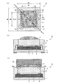
最初に、先の出願で開示した固体撮像装置80の構成及び製造方法について説明する。図8(a)は、固体撮像装置80の構成を示す平面図であり、図8(b)は、固体撮像装置80の構成を示す、X−X’における断面図であり、図8(c)は、固体撮像装置80の構成を示す、Y−Y’における断面図である。また、図9(a)は、固体撮像装置80の製造工程の内、一工程を説明するための図8(a)のX−X’における断面図であり、図9(b)は、固体撮像装置80の製造工程の内、一工程を説明するための図8(a)のY−Y’における断面図であり、図9(c)は、図9(b)のレンズ端部83a付近を拡大した断面図である。
First, the configuration and manufacturing method of the solid-
固体撮像装置80は、図8(a)(b)に示すように、下部に外部接続端子89が形成されたセンサ基板81、このセンサ基板81上に形成された固体撮像素子であるセンサチップ82、このセンサチップ82の有効画素領域91と対向するように配置された透明板であるガラス板84、上記センサチップ82とガラス板84とを平行に保持するスペーサ86、センサ基板81の一部、センサチップ82の一部、ガラス板84の側壁及びスペーサ96の側壁を封止する封止樹脂85、並びにガラス板84を覆う光学素子である樹脂製のレンズ83を備えている。
As shown in FIGS. 8A and 8B, the solid-
有効画素領域91は、スペーサ86に挟まれたセンサチップ82上の領域に形成されている。レンズ83は、紫外線の照射によって硬化する光硬化性樹脂83’を成形型に充填し、紫外線照射によって硬化させたものである。
The
センサチップ82の有効画素領域91、ガラス板84及びスペーサ86に囲まれた空間は、密閉された空気層87を形成している。ガラス板84は、空気層87への湿気、塵及び埃等の侵入、並びに製造工程において有効画素領域91に他の部材や製造装置の部品等が接触することによって生じる有効画素領域91の破損等から有効画素領域91を保護している。スペーサ86は、センサチップ82とガラス板84とに挟まれた熱硬化性樹脂を熱硬化させることによって形成する。このため、空気層87は完全に密閉されている。
A space surrounded by the
また、センサチップ82とセンサ基板81とは、ボンディングワイヤ88によって電気的に接続されている。すなわち、センサチップ82は、ボンディングワイヤ88、センサ基板81及び外部接続端子89を介して、外部へ電気信号を出力することができる。ボンディングワイヤ88も封止樹脂85によって封止されており、封止樹脂85は、ボンディングワイヤ88同士の接触や、ボンディングワイヤ88の断線等を防止している。
Further, the
封止樹脂85は、センサ基板81、センサチップ82、ガラス板84、スペーサ86、及びボンディングワイヤ88を組み立てた後、その周りに流し込むようにして成形される。その際、ガラス板84の上面(図8(b)に示す上方)への回り込みを防ぐために、封止樹脂85の上面はガラス板84の上面よりも下方に形成される。
The sealing
ここで、ボンディングワイヤ88は、センサチップ82のスペーサ86が形成された領域よりも外側に接続されている。このため、ガラス板84は、有効画素領域91を覆うことができるだけの平面寸法(サイズ)を有していれば、有効画素領域91を保護することができる。
Here, the
また、空気層87内部にボンディングワイヤ88を配置する必要がないので、空気層87を形成するスペーサ86の高さはガラス板84が有効画素領域91に接触しない程度であればよい。すなわち、ボンディングワイヤ88を空気層87内部に配置する必要がないので、固体撮像装置80の小型化及び薄型化(低背化)することができる。
Further, since it is not necessary to dispose the
さらに、固体撮像装置80の小型化を行うには、ガラス板84は有効画素領域91と同等の平面寸法(サイズ)である必要がある。ガラス板84が必要以上に大きいと、ボンディングワイヤ88と接触することになり、センサチップ82及びセンサ基板81を大型化し、接触を回避する設計が必要となる。結果的には、固体撮像装置80が大型化してしまうため、ガラス板84は有効画素領域91と同等の平面寸法であることが好ましい。
Furthermore, in order to reduce the size of the solid-
ガラス板84上に形成されたレンズ83は、凸レンズ状に形成されているので、レンズ83に入射した光を屈折させることによって、該光の角度が直角に近づくように補正することができる。光の入射する位置が、有効画素領域91の中心から離れるほど、その光の角度は垂直から離れる。有効画素領域91が入射光を認識し、電気信号に変換する効率は、入射光の角度が直角から離れるほど低くなるため、上記補正が必要になる。このため、レンズ83は、有効画素領域91の外周部における光の入射効率を高めるためには、有効画素領域91の全面を覆っている必要がある。
Since the
ここで、ガラス板84は、有効画素領域91と同等の平面寸法であるためレンズ83を形成すると、図8(a)(c)に示すように、レンズ83はガラス板84からはみ出て、封止樹脂85上にも形成される。
Here, since the
後述するが、レンズ83を傾けずにガラス板84上に形成するためには、レンズ成形型がガラス板84と接触する必要がある。そこで、ガラス板84に、露出した露出領域84aを設けている。
As will be described later, in order to form the
以上の構成から、図8(c)に示すように、ガラス板84の対角方向X−X’線の断面図では、レンズ83はガラス板84上に形成され、図8(b)に示すように、Y−Y’線の断面図では、レンズ83はガラス板84及び封止樹脂85の上に形成される。
From the above configuration, as shown in FIG. 8C, in the cross-sectional view taken along the line XX ′ in the diagonal direction of the
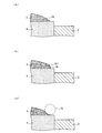
上記樹脂製のレンズ83を製造する方法について、図9(a)(b)(c)を用いて説明する。
A method for manufacturing the
レンズ83は、紫外線照射によって硬化する光硬化性樹脂83’から構成されている。レンズ83は、光硬化性樹脂83’を成形型92の窪みに充填し、成形型92の平坦部をガラス板84に接触させた状態で紫外線を照射することによって形成されている。
The
図8(a)に示すガラス板84の対角方向X−X’では、図9(a)に示すように、成形型92をガラス板84に接触させることによって、成形型92とガラス板84との距離の調整を行うと共に、相互傾きを低減することができる。これにより、レンズ83とガラス板84との調整を行うことが可能となる。
In the diagonal direction XX ′ of the
図8(a)に示すガラス板84のY−Y’では、図9(b)に示すように、ガラス板84が成形型92の窪みよりも小さいため、レンズ83は封止樹脂85に形成される。
In YY ′ of the
上記封止樹脂85の上に形成されたレンズ端部83aの拡大図を、図9(c)に示す。成形型92の平坦面とガラス板84とは、上述の通り、一致している。ここで、ガラス板84の上面と封止樹脂85の上面との間にはギャップGがあり、成形型92の平坦面と封止樹脂85とは接触していない。
An enlarged view of the
しかしながら、上記構成の固体撮像装置80においては、以下の課題を有している。
However, the solid-
まず、光硬化性樹脂83’は、硬化前は流動体であるので、該光硬化性樹脂83’は、成形型92及びガラス板84への接触時に、毛細管力及び光硬化性樹脂83’にかかる重力によって成形型92の窪みからギャップGを通して流れ出る。この現象により、レンズ83形成に必要な樹脂量を確保することができなくなり、レンズ83の一部に窪み及び気泡が発生し、所望のレンズ形状を得ることができないという課題を生ずる。
First, since the
次に、光硬化性樹脂には、シリコーン樹脂等、酸素による硬化阻害により、大気中(酸素雰囲気中)では硬化しない樹脂が多くある。本構成では、ギャップGにおいて硬化前の光硬化性樹脂83’が大気と接触するため、ギャップG付近の光硬化性樹脂83’が硬化しないといった課題を生じる。また、酸素による効果阻害のない光硬化性樹脂に選択肢を制限され、自由度のある設計を行うことができないといった課題を同時に生じる。
Next, many photocurable resins, such as silicone resins, do not cure in the air (in an oxygen atmosphere) due to inhibition of curing by oxygen. In this configuration, the photo-curing
一方、上述のように、レンズ端部83aが封止樹脂85の一部と接着しているが、レンズ83と封止樹脂85との接着力は小さい。これは以下の2つの理由による。
(1)封止樹脂85が図示しない金型を用いて圧縮形成された後にレンズ83が形成されるため、レンズ83の形成時に封止樹脂85が化学的に活性を有していない。
(2)封止樹脂85の成形終了後に、封止樹脂85とそれを形成するための金型とが剥がれ易くなるように、封止樹脂85表面には離型剤が付着している。さらに、レンズ83と封止樹脂85とは、異なる樹脂から構成されているので、熱膨張係数が異なる。
On the other hand, as described above, the
(1) Since the
(2) After the molding of the sealing
したがって、レンズ83を封止樹脂85上に形成すれば、固体撮像装置80の実装工程における加熱冷却処理や固体撮像装置80を内蔵した製品を使用する環境温度の変化によって、レンズ端部83aが封止樹脂85から剥離する。
Therefore, if the
この結果、レンズ端部83aが封止樹脂85から剥離することによって、レンズ83が変形し、所望の光学特性を得ることができないといった課題を生じる。また、封止樹脂85とレンズ端部83aの樹脂との接着性が悪いため、該箇所でレンズ端部83aの樹脂が金型へ付着し、金型の洗浄が必要となる。
As a result, the
このように、固体撮像装置80においては、種々の課題が残されている。
As described above, various problems remain in the solid-
〔実施の形態1〕
本発明の一実施形態について図1〜図7に基づいて説明すれば、以下の通りである。
[Embodiment 1]
An embodiment of the present invention will be described below with reference to FIGS.
本実施の形態の固体撮像装置は、前記参考形態に記載の固体撮像装置80の課題を解決するものとなっている。
The solid-state imaging device according to the present embodiment solves the problem of the solid-
本実施の形態の固体撮像装置10の構成及び形成方法について、図1(a)(b)(c)及び図2(a)(b)(c)を用いて以下に説明する。図1(a)は、固体撮像装置10の構成を示す平面図であり、図1(b)は、固体撮像装置10の構成を示す、図1(a)のA−A’線における断面図であり、図1(c)は、固体撮像装置10の製造工程の内、一工程を説明するための図1(a)のA−A’線における断面図である。また、図2(a)は、図1(a)に示す固体撮像装置10のレンズ3のレンズ角端部3a付近を拡大した断面図であり、図2(b)(c)は、図1(a)に示す固体撮像装置10のレンズ3のレンズ角端部3a付近を拡大した断面図である。
The configuration and formation method of the solid-
本実施の形態の固体撮像装置10は、図1(b)に示すように、下部に外部接続端子9が形成されたセンサ基板1、このセンサ基板1上に形成された固体撮像素子としてのセンサチップ2、このセンサチップ2の有効画素領域11と対向するように配置されたガラス板等の透明板としての透明基板4、上記センサチップ2と透明基板4とを平行に保持するスペーサ6、センサ基板1の一部、センサチップ2の一部、透明基板4の側壁及びスペーサ6の側壁を封止する封止樹脂5、並びに透明基板4を覆う樹脂製の光学素子としてのレンズ3を備えている。
As shown in FIG. 1B, the solid-
上記センサチップ2の有効画素領域11は、スペーサ6に挟まれたセンサチップ2上の領域に形成されている。レンズ3は、紫外線の照射によって硬化する光硬化性樹脂3’を後述する成形型22に充填し、紫外線照射によって硬化させたものである。
The
センサチップ2の有効画素領域11、透明基板4及びスペーサ6に囲まれた空間は、密閉された空気層7を形成している。透明基板4は、空気層7への湿気、塵及び埃等の侵入、並びに製造工程において有効画素領域11に他の部材や製造装置の部品等が接触することによって生じる有効画素領域11の破損等から有効画素領域11を保護している。スペーサ6は、センサチップ2と透明基板4とに挟まれた熱硬化性樹脂を熱硬化させることによって形成する。このため、空気層7は完全に密閉されている。
A space surrounded by the
上記センサチップ2とセンサ基板1とは、ボンディングワイヤ8によって電気的に接続されている。すなわち、センサチップ2は、ボンディングワイヤ8、センサ基板1及び外部接続端子9を介して、外部へ電気信号を出力することができる。ボンディングワイヤ8も封止樹脂5によって封止されており、封止樹脂5は、ボンディングワイヤ8同士の接触や、ボンディングワイヤ8の断線等を防止している。
The
ここで、ボンディングワイヤ8は、センサチップ2のスペーサ6が形成された領域よりも外側に接続されている。このため、透明基板4は、有効画素領域11を覆うことができるだけの平面寸法(サイズ)を有していれば、有効画素領域11を保護することができる。
Here, the
さらに、空気層7内部にボンディングワイヤ8を配置する必要がないので、空気層7を形成するスペーサ6の高さは透明基板4が有効画素領域11に接触しない程度であればよい。すなわち、ボンディングワイヤ8を空気層7内部に配置する必要がないので、固体撮像装置10の小型化及び薄型化(低背化)することができる。
Furthermore, since it is not necessary to arrange the
透明基板4上に形成されたレンズ3は、凸レンズ状に形成されているので、レンズ3に入射した光を屈折させることによって、該光の角度が直角に近づくように補正することができる。光の入射する位置が、有効画素領域11の中心から離れるほど、その光の角度は垂直から離れる。有効画素領域11が入射光を認識し、電気信号に変換する効率は、入射光の角度が直角から離れるほど低くなるため、上記補正が必要になる。このため、レンズ3は、有効画素領域11の外周部における光の入射効率を高めるためには、有効画素領域11の全面を覆っている必要がある。
Since the
次に、本実施の形態の固体撮像装置10の主たる特徴点について、図1(a)を用いて以下に説明する。
Next, main feature points of the solid-
本実施の形態の固体撮像装置10は、図1(a)に示すように、固体撮像装置10の側面及び上面の一部を覆う封止樹脂5、封止樹脂5に取り囲まれた透明基板4、この透明基板4上に形成された樹脂製のレンズ3、及びレンズ3と透明基板4とを透過した光が入射する前記センサチップ2の有効画素領域11を備えている。
As shown in FIG. 1A, the solid-
上記有効画素領域11は、対向する1組の辺が長さW1を有し、かつ他の1組の辺が長さW2を有している。透明基板4の上面は、対向する1組の辺が長さW3を有し、かつ他の1組の辺が長さW4を有している。長さW1と長さW3との差は、又は長さW2と長さW4との差は、スペーサ6の幅に等しい。つまり、透明基板4の上面のサイズ(W3×W4)は、有効画素領域11のサイズ(W1×W2)にスペーサ6上面のサイズを加えたものであり、上述のように、透明基板4の上面のサイズと有効画素領域11のサイズは同等程度であり、詳しくは透明基板4の上面のサイズは有効画素領域11のサイズよりもスペーサ6の分だけ大きい。また、透明基板4はボンディングワイヤ8に接触しない必要があるため、該センサ基板1のサイズよりも小さい。
In the
透明基板4の上面のサイズ(W3×W4)と有効画素領域11のサイズ(W1×W2)とは殆ど変わらないので、有効画素領域11の全体を覆うようにレンズ3を形成すると、円形状のレンズではレンズ外周部が透明基板4からはみ出す。ここで、レンズ3が透明基板4の上面を全て覆っている必要はなく、有効画素領域11上にあればよい。
Since the size (W3 × W4) of the upper surface of the
また、光硬化性樹脂3’が成形時に封止樹脂5上に存在すると、前記参考形態で述べた固体撮像装置80のように、いくつかの課題が生じる。
In addition, when the
そこで、本実施の形態の固体撮像装置10では、レンズ3は有効画素領域11上を覆っており、かつ封止樹脂5上にかかることなく、透明基板4の外形部よりも内側で形成されることとしている。換言すると、図1(a)に示すように、レンズ3の外形が有効画素領域11の外側かつ透明基板4の外形よりも内側に形成されるようにしている。
Therefore, in the solid-
本実施の形態においては、レンズ3は、紫外線照射によって硬化する光硬化性樹脂3’から構成されている。ここで、レンズ3は、図1(c)に示すように、光硬化性樹脂3’を成形型22の窪みに充填し、成形型22の平坦部を透明基板4に接触させた状態で紫外線を照射することによって形成されている。
In the present embodiment, the
上記レンズ3は、固体撮像装置10に入射する光の角度を直角に近づくように補正するためのものであり、レンズ3の中心を透過する光が有効画素領域11へ直角に入射するように形成される必要がある。入射光の角度の補正を適切に行えるようにレンズ3を形成するためには、成形型22の平坦部22a(図1(c)の破線で囲んだ箇所)を有効画素領域11と平行な面に接触させる必要がある。
The
本実施の形態では、透明基板4は、有効画素領域11と対向するようにスペーサ6を介してセンサチップ2に接着されている。透明基板4が平行平面状であること、及びスペーサ6が均一な厚さを有する非常に薄い構成であることから、透明基板4の上面は有効画素領域11と平行である。
In the present embodiment, the
また、本実施の形態では、レンズ3は、成形型22の平坦部が有効画素領域11と平行な透明基板4の上面に接触した状態で形成されているため、レンズ3の中心を透過する光を正確に有効画素領域11に対して直角に入射させることができる。つまり、透明基板4にレンズ3からの露出部を有しているため、レンズ3の取り付け精度を高めることができる。
In the present embodiment, the
一般的に、透明基板4の上面の形状が、長さW4が長さW3よりも僅かに長い長方形を有している。同様に、有効画素領域11の形状は、長さW2が長さW1よりも僅かに長い長方形を有している。尚、本実施の形態において、有効画素領域11(透明基板4上面)が長方形を有する固体撮像装置10について説明しているが、必要に応じて、有効画素領域11(透明基板4上面)の形状を適宜変更すればよい。
Generally, the shape of the upper surface of the
ここで、図2(a)を用いて、図1(a)に示すレンズ3のレンズ角端部3aの構成を説明する。
Here, the configuration of the lens
本実施の形態では、レンズ3は有効画素領域11の対角間距離が光学有効径として設計されている。すなわち、レンズ3は、有効画素領域11の中心を光学中心とし、直径を有効画素領域11の対角間距離として、外形を円形状にして設計される。なお、レンズ外形は、円に限らず、楕円でもよい。
In the present embodiment, the
上記レンズ3は凸レンズ形状であるため、図1(a)におけるA−A’線で示す透明基板4の対角方向においては、図2(a)に示すように、レンズ稜線は有効径外側近傍で透明基板4と交わる。
Since the
次に、図2(b)を用いて、図1(a)に示すレンズ3のレンズ辺端部3bの構成を説明する。
Next, the configuration of the lens
上述のように、レンズ3は有効画素領域11の対角間距離を光学有効径として設計されるが、このまま円形のレンズ3としてしまうと、レンズ3の平面形状が透明基板4の平面形状よりも大きくなり、封止樹脂5に形成され、前記参考形態にて説明した固体撮像装置80の課題となる。
As described above, the
そこで、本実施の形態では、有効画素領域11の対角方向以外の方向においては、有効画素領域11上以外の領域において設計形状とは異なった形状を取る必要があり、レンズ3の稜線が透明基板4と交わる設計とする。
Therefore, in the present embodiment, in the direction other than the diagonal direction of the
具体的には、図2(b)に示すように、レンズ3のレンズ辺端部3bを断面が直線SL1となるように形成する。この直線SL1は、センサチップ2に近づくに伴ってレンズ3外側に広がる方向の傾きを持つ。この勾配構造により、光硬化性樹脂3’硬化後の離型時に必要な力を低減することができると共に、曲面形状から直線形状に切り替わる極値を設けることができるため、この部分をレンズ3の位置調整及び検査を行う際のマーカーとして使用することができる。
Specifically, as shown in FIG. 2B, the lens
尚、レンズ辺端部3bにおける他の稜線の形状としては、図2(c)に示すように、透明基板4の上面を接線とする円CLを形状の一部としてもよい。また、レンズ辺端部3bのさらに他の稜線の形状としては、直線SL1と円CLとを組み合わせたものでもよい。
In addition, as a shape of the other ridgeline in the lens
レンズ3の外形形状についてまとめると、レンズ3の外形形状は、図1(a)に示すように、有効画素領域11の対角方向については、有効画素領域11の中心を光学中心とし、直径を有効画素領域11の対角間距離として設計された、レンズの円形状外形の一部からなる。また、有効画素領域11の対角方向以外の方向については、レンズ3の外形形状は、有効画素領域11及び透明基板4の各4辺と平行な直線で構成される。
Summarizing the outer shape of the
以上において、本実施の形態の固体撮像装置10の主な構成について説明した。
The main configuration of the solid-
次に、固体撮像装置10のより好ましい構成及び固体撮像装置10に採用可能な構成について以下に説明する。
Next, a more preferable configuration of the solid-
本実施の形態においては、レンズ3は紫外線の照射によって硬化する光硬化性樹脂3’を用いているが、レンズ3を構成する樹脂としては、必ずしもこれに限らず、紫外線を除く光の照射によって硬化する光硬化性樹脂3’であってもよく、さらに、熱エネルギーの付与によって硬化する熱硬化性樹脂であってもよい。
In the present embodiment, the
また、本実施の形態のレンズ3を構成する樹脂としては、エネルギーを付与することによって硬化する樹脂であり、硬化した後に光透過性を有する樹脂であれば従来公知の樹脂から適宜選択し得る。尚、本明細書において、光硬化性樹脂3’及び熱硬化性樹脂を総称して「エネルギー硬化性樹脂」と記載する場合がある。
Moreover, as resin which comprises the
さらに、本実施の形態の固体撮像装置10においては、上記レンズ3は、−60℃〜270℃の温度条件において、80%以上の可視光の透過率を有していることが好ましい。
Furthermore, in the solid-
すなわち、−60℃〜270℃の温度条件において、レンズ3を構成する樹脂が変性した場合、80%以上の可視光の透過率を有していない場合には、固体撮像装置10を適切に補正し得なくなる。しかし、レンズ3が−60℃〜270℃の温度条件において、80%以上の可視光の透過率を有しているという構成を有することによって、レンズ3が上記温度条件に曝された場合であっても、固体撮像装置10に入射する光を、固体撮像装置10にほぼ垂直に入射するように補正するというレンズ3の作用を維持し得る。
That is, when the resin constituting the
ここで、レンズ3を形成しない場合、固体撮像装置10は、通常、その外部接続端子9とフレキシブルプリント基板(FPC:flexible printed circuits)等の基板上の配線とをリフロー処理によって半田を熔解及び凝固させることによって基板に実装される。リフロー処理の後、固体撮像装置10に光学レンズを搭載することによって撮影素子(カメラモジュール)を作製する。
Here, when the
固体撮像装置10のリフロー処理による実装は、例えば、固体撮像装置10をフレキシブルプリント基板(FPC)等にマウントする場合には、無鉛半田リフロー実装工程を、図3に示すような温度プロファイルで行う。
For example, when the solid-
上記条件を満たす樹脂としては、アルキル基及び/又はフェニル基及び/又はメチル基及び/又はメタクリル基を有するシリコーン樹脂、並びに炭素骨格とシリコーン骨格とがハイブリッドされた有機無機ハイブリッドシリコン樹脂等のエネルギー硬化性樹脂を挙げることができる。 Examples of the resin satisfying the above conditions include energy curing such as a silicone resin having an alkyl group and / or a phenyl group and / or a methyl group and / or a methacryl group, and an organic-inorganic hybrid silicone resin in which a carbon skeleton and a silicone skeleton are hybridized. Can be mentioned.
すなわち、例示したような材料から光学素子を構成することによって、透明板上に光学素子を形成した状態であっても、リフロー処理によって固体撮像装置10を基板に実装することができる。
That is, by configuring the optical element from the exemplified materials, the solid-
本実施の形態では、レンズ3は、エネルギー硬化性樹脂である光硬化性樹脂3’を成形型22に充填し、この成形型22を透明基板4及び封止樹脂5を接触させた状態で硬化させることによって形成されている。このため、レンズ3は、所望の形状に形成することが容易である。レンズ3の凸面の形状としては、レンズ3に入射する光を、有効画素領域11に垂直に出射し得るように補正する形状であればよく、球面又は非球面であってもよい。例えば、レンズ3は、パワーを有する非球面レンズ、フレネル形状を有するレンズ及び微細なレリーフ形状が施された回折レンズとして形成されていてもよい。
In the present embodiment, the
また、透明基板4上には、シランカップリング剤が付与されていることが好ましい。上記透明基板4に付与するシランカップリング剤は、レンズ3との化学的な接着力を向上し得るのもであればよく、従来公知のシランカップリング剤から、レンズ3を構成する樹脂の性質に合わせて、適宜選択すればよい。レンズ3と透明基板4との接着力を向上させるシランカップリング剤としては、エポキシ系やアミノ系のシランカップリング剤が好ましい。
Moreover, it is preferable that a silane coupling agent is provided on the
上記シランカップリング剤の透明基板4への付与は、以下のように行えばよい。
The silane coupling agent may be applied to the
まず、シランカップリング剤をイソプロピルアルコール等の有機溶媒によって1%程度に希釈する。次いで、希釈したシランカップリング剤に透明基板4の上面を浸漬(ディップ)する。そして、シランカップリング剤をディップした透明基板4を乾燥させることによって、透明基板4にシランカップリング剤を付与することができる。尚、ここで説明した方法以外にも、従来公知の方法を用いて透明基板4にシランカップリング剤を付与することができる。
First, the silane coupling agent is diluted to about 1% with an organic solvent such as isopropyl alcohol. Next, the upper surface of the
また、上記シランカップリング剤は、後述する赤外波長カット膜としての赤外線カットフィルタとレンズ3との間に付与することも可能である。これにより、赤外波長カット膜とレンズ3との付着性を高めることができる。
The silane coupling agent can be applied between an infrared cut filter as an infrared wavelength cut film, which will be described later, and the
さらに、上記センサチップ2の有効画素領域11上には、マイクロレンズが形成されていることが好ましい。
Furthermore, it is preferable that a microlens is formed on the
上記構成を有することによって、レンズ3から出射された(出射角度が補正された)光を、さらに、上記マイクロレンズによって有効画素領域11に入射する光の角度を補正することができる。したがって、固体撮像装置10の有効画素領域11に入射する光をより最適な状態に補正することができる。
By having the above configuration, it is possible to further correct the angle of light emitted from the lens 3 (the emission angle is corrected) and incident on the
さらに、固体撮像装置10を撮影装置に適用する場合、上記マイクロレンズの形成位置等も考慮に入れて、撮影装置全体の光学系(レンズ3、マイクロレンズ及び撮影用レンズ等)の設計(形状及び配置等)を行うことが好ましい。
Further, when the solid-
また、透明基板4とレンズ3の間には、赤外波長カット膜としての赤外線カットフィルタが形成されていることが好ましい。
In addition, an infrared cut filter as an infrared wavelength cut film is preferably formed between the
すなわち、カメラやビデオレコーダーカメラ等の撮影装置に固体撮像装置10を内蔵させる場合、画像の形成に不要な赤外線がセンサチップ2へ入射することを回避する必要がある。赤外線のセンサチップ2への入射を回避するためには、赤外線を反射及び/又は吸収(カット)する必要がある。ここでは、赤外線を反射するための誘電体多層膜を透明基板4とレンズ3との間に形成することを例として、以下に説明を行う。
That is, when the solid-
上記誘電体多層膜は、光の入射角に応じて、反射する光の波長の範囲が変化する。このため、曲面(例えば、レンズ3等)上に誘電体多層膜を形成すると、中心付近と端部付近とにおいて反射する光の波長が異なるため、逆に画質の悪化に繋がる。このため、平坦な透明基板4上に形成することが好ましい。
In the dielectric multilayer film, the range of the wavelength of reflected light changes according to the incident angle of light. For this reason, when a dielectric multilayer film is formed on a curved surface (for example, the lens 3), the wavelength of the reflected light is different between the vicinity of the center and the vicinity of the end portion. For this reason, it is preferable to form on the flat
また、上記誘電体多層膜は、透明基板4におけるレンズ3を形成するための面に製膜される。透明基板4の有効画素領域11との対向面に誘電体多層膜を形成すると、誘電体多層膜が剥離を起こした場合、有効画素領域11に付着することによって、画質を低下させるためである。
The dielectric multilayer film is formed on the surface of the
尚、透明基板4だけに誘電体多層膜を形成すると、誘電体多層膜の膜応力によって、透明基板4に反りが生じる。しかし、大面積の透明基板4に誘電体多層膜を製膜した後、透明基板4はダイシングによって小片に分割されるので、上記膜応力を開放(低下)し得る。このため、誘電体多層膜の形成による透明基板4の反りは、固体撮像装置10によって形成される画像の質を低下させることはない。ここで、赤外線反射の誘電体多層膜は、スパッタ法や蒸着法等によって、高い屈折率の層と低い屈折率の層とが交互に形成された多層膜である。
If the dielectric multilayer film is formed only on the
また、透明基板4としては、平行平面板状の透明な部材であればよく、ガラスに限らず、樹脂等から構成されていてもよい。
Further, the
さらに、センサ基板1は、絶縁性を有する平板状の構成であればよく、センサ基板1全体が絶縁性の材料から構成されていても、センサ基板1表面が絶縁性を有していてもよい。上記センサ基板1を構成するための材料は、セラミックや樹脂等、従来公知の種々の材料から選択することができる。また、センサ基板1表面に絶縁性を付与する方法は、従来公知の種々の方法を採用し得る。 Furthermore, the sensor substrate 1 may be a flat plate-like structure having an insulating property, and the entire sensor substrate 1 may be made of an insulating material or the surface of the sensor substrate 1 may have an insulating property. . The material for constructing the sensor substrate 1 can be selected from conventionally known various materials such as ceramic and resin. Moreover, conventionally well-known various methods can be employ | adopted for the method of providing insulation to the sensor substrate 1 surface.
また、スペーサ6は、センサチップ2と透明基板4とを平行に保持し得る材料であればよく、例えば、接着性を有する材料等、従来公知の種々の材料から選択できる。尚、透明基板4以外の部材から光が入射することがないように、スペーサ6は不透明な材料から構成されていることが好ましい。
Moreover, the
さらに、封止樹脂5を構成する材料としては、従来公知の種々の樹脂から選択すればよい。尚、透明基板4以外の部材から光が入射することがないように、封止樹脂5は不透明な材料から構成されていることが好ましい。また、封止樹脂5を形成するための方法としては、従来公知の種々の方法を採用すればよい。
Furthermore, what is necessary is just to select as a material which comprises the sealing
すなわち、樹脂封止後の未完成の固体撮像装置(以下、単に固体撮像装置と称する)にレンズ3を形成する工程は、例えば、図4(a)〜図4(d)の順に行われる。
That is, the process of forming the
まず、図4(a)に示すように、固体撮像装置10を、透明基板4が下方を向くように、図示しないマウンター装置のロッド21を用いて真空固定(バキュームチャッキング)する。同時に、透明な成形型22のレンズ3の表面形状を転写するために形成された窪みに流動性を有する光硬化性樹脂3’を充填する。
First, as shown in FIG. 4A, the solid-
ここで、本実施の形態においては、レンズ3を構成する樹脂として、紫外線の照射によって硬化する光硬化性樹脂3’を例に説明しているが、エネルギー硬化性樹脂であれば、本発明の固体撮像装置の製造方法に適用することができる。
Here, in the present embodiment, as the resin constituting the
次いで、図4(b)に示すように、透明な成形型22、光硬化性樹脂3’及び透明基板4を介して、カメラ23を用いて有効画素領域11の形状(平面形状及び中心の位置等)を撮像する。撮像した有効画素領域11の形状を画像処理装置によって画像処理を行う。次いで、マーキングを用いて上記画像処理装置に予め認識させておいた透明な成形型22の中心と画像処理した有効画素領域11の中心とをX軸方向及び/又はY軸方向に位置合わせする。尚、透明基板4には、光硬化性樹脂3’を固着する前に、シランカップリング剤が付与されていてもよい。
Next, as shown in FIG. 4B, the shape (planar shape and center position) of the
上記位置合わせの終了後、図4(c)に示すように、光硬化性樹脂3’を充填した透明な成形型22を透明基板4に接触した状態で固定する。透明な成形型22を固定した後、UV(Ultra Violet)ランプ24を点灯し、紫外線照射を行う。
After completion of the alignment, as shown in FIG. 4C, the
UVランプ24による紫外線の照射によって、透明な成形型22に充填された光硬化性樹脂3’が硬化する。
By irradiating the
光硬化性樹脂3’が十分に硬化することによって、レンズ3が形成された後、図4(d)に示すように、透明な成形型22を固体撮像装置10から離型させる。
After the
本実施の形態の製造方法を用いれば、パワーを有する非球面レンズ、フレネル形状を有するレンズ及び微細なレリーフ形状が施された回折レンズ等、複雑な形状を有するレンズ3を容易に形成することができる。さらに、レンズ3の中心が有効画素領域11の中心と正確に対向するように位置合わせをしながら、レンズ3を形成することができるので、収差が小さく、かつ解像度の高い画像を形成することができる固体撮像装置10を提供することができる。
By using the manufacturing method of the present embodiment, it is possible to easily form a
したがって、簡便で安価な方法を用いて、小型化及び薄型化を達成し、かつ高い信頼性(耐環境性)及び性能を付与した固体撮像装置10及びその製造方法を提供することができる。
Therefore, it is possible to provide a solid-
このように、本実施の形態の固体撮像装置10では、有効画素領域が形成されたセンサチップ2と、センサチップ2の有効画素領域と対向するように配置された透明基板4と、センサチップ2の一部、及び透明基板4の側壁を封止する封止樹脂5と、透明な樹脂から構成されたレンズ3とを備え、レンズ3は、透明基板4上に形成され、かつレンズ3の光軸方向から見たときに、レンズ3の外周は透明基板4の外周よりも光軸中心側に形成されている。
Thus, in the solid-
また、本実施の形態の固体撮像装置10の製造方法では、センサチップ2の有効画素領域と対向するように、かつセンサチップ2の平面形状の内側に存在するように透明基板4を配設する第1の工程と、センサチップ2の一部、及び透明基板4の側壁を封止樹脂5により封止する第2の工程と、透明基板4上に透明な樹脂から構成されたレンズ3を形成する第3の工程とを含み、第3の工程においてレンズ3と封止樹脂5とは接しない。
Further, in the method for manufacturing the solid-
この構成によれば、レンズ3は、透明基板4上に形成され、かつレンズ3の光軸方向から見たときに、レンズ3の外周は透明基板4の外周よりも光軸中心側に形成されている。
According to this configuration, the
したがって、レンズ3が透明基板4上に形成されているので、センサチップ2の周辺部への入射光が暗くなることを抑制することができる。
Therefore, since the
また、レンズ3は、透明基板4と同じ外周の側壁を有していないので、センサチップ2の有効画素領域へ入射する迷光を抑制することができる。
Further, since the
また、例えば、レンズ3を流動体の光硬化性樹脂3’にて硬化させて形成する場合、光学素子成形時には、成形型22に光硬化性樹脂3’を充填し、成形型22と透明基板4とを接触させて硬化させる。その際、本実施の形態では、レンズ3は透明基板4上に形成され、封止樹脂5上には形成されない。したがって、透明基板4の上面と封止樹脂5の上面との段差部に光硬化性樹脂3’が接触するということがなく、これによって、該段差から樹脂が漏れ出して所望の光学素子形状を得ることができないということがない。
Further, for example, when the
さらに、光硬化性樹脂3’は、成形型22と透明基板4とで密閉され大気に触れることがない。これにより、例えば、酸素による硬化阻害が起きる光硬化性樹脂3’を選択することができ、自由度のある設計を行うことができる。この結果、信頼性のある高性能な固体撮像装置10の製造方法を提供することができる。
Furthermore, the
また、封止樹脂5とレンズ3とが接しないことにより、レンズ3が封止樹脂5から剥がることがない点において、高い信頼性及び耐環境性能を持った固体撮像装置10とすることができる。
Further, since the sealing
したがって、センサチップ2の周辺部への入射光が暗くなることを抑制し、かつセンサチップ2の有効画素領域へ入射する迷光を抑制し、さらに、高い信頼性を得ることができる固体撮像装置10、及び固体撮像装置10の製造方法を提供することができる。
Therefore, the solid-
本実施の形態の固体撮像装置10では、レンズ3は、レンズ3の光軸方向から見たときに、レンズ3の外周がセンサチップ2の有効画素領域の外側になるように形成されている。
In the solid-
これにより、レンズ3は、センサチップ2の有効画素領域の全面を覆っている。この結果、レンズ3においても、センサチップ2の有効画素領域における対応平面領域の外周部に入射した光を屈折させて、光の角度が直角に近づくように補正することができる。したがって、センサチップ2の周辺部への入射光が暗くなることを確実に抑制することができる。
Thus, the
また、本実施の形態の固体撮像装置10では、透明基板4は、センサチップ2の平面形状の内側に存在するように配設されている。
Moreover, in the solid-
これにより、透明基板4の面積をセンサチップ2の面積よりも小さくすることによって、固体撮像装置10もそれに応じて小さくなり、結果的に、この固体撮像装置10を備える後述する撮影装置50も小型のものを提供することができる。
Thereby, by making the area of the
また、本実施の形態の固体撮像装置10では、レンズ3は、レンズ3の光軸方向から見たときに、レンズ3の外周が曲線で形成されているとすることができる。
In the solid-
これにより、例えば、レンズ3を流動体の光硬化性樹脂3’にて硬化させて形成する場合、レンズ3の形成時に使用する成形型22の内形は、急激な変曲点が存在せず連続しているため、切削時に欠けが生じ難く、容易に作製が可能である。したがって、成形型22の作製において、低コストを図り得る固体撮像装置10を提供することができる。
Thereby, for example, when the
また、本実施の形態の固体撮像装置10では、レンズ3は、レンズ3の光軸方向から見たときに、レンズ3の外周が1つ以上の直線を含んで形成されているとすることができる。
Further, in the solid-
これにより、レンズ3の外周として曲線よりも直線を用いることによって、レンズ3の中心の認識が容易となり、レンズ3の形成時及び検査時に、後述する撮影装置50との位置調整用のマーカーとして機能することが可能となり、短時間で高精度な位置調整を行った低コスト、かつ高性能の固体撮像装置10を提供することができる。
Accordingly, by using a straight line rather than a curve as the outer periphery of the
また、本実施の形態の固体撮像装置10では、レンズ3は、レンズ3の光軸方向から見たときに、レンズ3の外周が曲線と1つ以上の直線とで形成されているとすることができる。
Further, in the solid-
これにより、一般的に長方形であるセンサチップ2の有効画素領域と、その有効画素領域よりも少し広めの長方形である透明基板4との間に、レンズ3の外形を形成することができる。したがって、センサチップ2の有効画素領域と同等程度の大きさの透明基板4を採用することができ、小型の固体撮像装置10を提供することができる。
Thus, the outer shape of the
また、本実施の形態の固体撮像装置10では、レンズ3は、センサチップ2の有効画素領域内に形成された有効領域と、それ以外の非有効領域とからなり、レンズ3の有効領域は、撮像系における有効光束を屈折させてセンサチップ2の有効画素領域に導く一方、レンズ3の非有効領域は、有効光束に関与しないように形成されている。
In the solid-
これにより、レンズ3の非有効領域を通過した光束は撮像に関係しない構成となり、非有効領域のレンズ3の形状を任意の形状に設計することができる。したがって、例えば、成形型22からレンズ3が離型し易い構造等、成形型22の成形が容易になり、高スループットで低コストの固体撮像装置10を提供することができる。
Thereby, the light flux that has passed through the ineffective area of the
また、本実施の形態の固体撮像装置10では、レンズ3は、有効領域の断面形状と非有効領域の断面形状との間に変曲点を有して互いに異なる曲率又は勾配を有すると共に、非有効領域において透明基板4面と交わっているとすることができる。
In the solid-
これにより、レンズ3の非有効領域における形状を自由に設定できるので、成形型22及びレンズ3の設計の簡略化を図ることができ、短期間で固体撮像装置10を提供することができる。
Thereby, since the shape in the ineffective area | region of the
また、本実施の形態の固体撮像装置10では、レンズ3は、非有効領域の断面形状において、透明基板4の表面を接線とする円の一部を、形状の一部としているとすることができる。
Further, in the solid-
これにより、レンズ3の非有効領域の断面形状を部分的に透明基板4の表面を接線とする円に変更することによって、レンズ3の外形が透明基板4内に収まることが可能になると共に、徐々に端部のレンズ3の厚みが減少する形状となるため、離型時に端部に応力が集中せず、離型が容易になる。この結果、高スループットで低コストの固体撮像装置を提供することができる。
Accordingly, by changing the cross-sectional shape of the ineffective area of the
また、本実施の形態の固体撮像装置10では、レンズ3は、非有効領域の断面形状において、レンズ3からセンサチップ2に近づくに伴ってレンズ3の光軸から遠ざかる方向の直線SL1を、形状の一部としているとすることができる。
Further, in the solid-
これにより、レンズ3の非有効領域の断面形状を途中から直線に変更することによって、レンズ3の外形が透明基板4内に収まることが可能になると共に、断面形状におけるその直線SL1とレンズ3の曲線との境界を、レンズ3の形成時及び検査時に、後述する撮影装置50との位置調整用のマーカーとして機能させることができる。この結果、短時間で高精度な位置調整を行った低コストかつ高性能の固体撮像装置10を提供することができる。
Thereby, by changing the cross-sectional shape of the ineffective area of the
また、本実施の形態の固体撮像装置10では、透明基板4におけるレンズ3側の表面には、シランカップリング剤が付与されていることが好ましい。
In the solid-
これにより、シランカップリング剤によって、例えば、無機材料である透明基板4と有機材料であるレンズ3との接着力を向上させ、耐環境性能の高い固体撮像装置10を提供することができる。
Thereby, for example, the adhesive force between the
また、本実施の形態の固体撮像装置10では、透明基板4のレンズ3側には、図示しない赤外波長カットフィルタが設けられていることが好ましい。
In the solid-
これにより、固体撮像装置10が、近赤外線を電気信号に変換し、解像度の低下や画像のムラ等画質の劣化を引き起こすということがなくなる。
As a result, the solid-
また、本実施の形態の固体撮像装置10では、図示しない赤外波長カットフィルタとレンズ3との間には、シランカップリング剤が付与されていることが好ましい。
Moreover, in the solid-
これにより、シランカップリング剤により、無機材料である赤外波長カットフィルタと有機材料であるレンズ3との接着力を向上させ、耐環境性能の高い固体撮像装置を提供することができる。
Thereby, the adhesive force of the infrared wavelength cut filter which is an inorganic material and the
また、本実施の形態の固体撮像装置10では、レンズ3は、−60℃〜270℃の温度条件において、80%以上の可視光の透過率を有していることが好ましい。
Moreover, in the solid-
これにより、レンズ3を実装したまま、固体撮像装置10におけるその外部接続端子9とFPC等の基板上の配線とをリフロー処理によって半田を熔解及び凝固させて、固体撮像装置10を基板に実装することができる。したがって、製造工程が簡略化されるので、低コストの固体撮像装置10を提供することができる。
As a result, with the
また、本実施の形態の固体撮像装置10の製造方法では、前記第3の工程は、流動性を有するエネルギー硬化性樹脂を成形型に充填する第1の処理と、光エネルギー又は熱エネルギーの付与によって上記エネルギー硬化性樹脂を硬化する第2の処理とを含む。
Further, in the method for manufacturing the solid-
これにより、エネルギー硬化性樹脂を充填した成形型22を用いてレンズ3を形成することができる。このため、所望の形状を有するレンズ3の、例えば、パワーを有する非球面レンズ、フレネル形状を有するレンズ及び微細なレリーフ形状が施された回折レンズ等の凸面を容易に形成することができる。
Thereby, the
また、本実施の形態の固体撮像装置10の製造方法では、前記第2の処理を、透明な成形型22を用いてレンズ3を形成すべき位置を確認しながら行うことが好ましい。
In the method for manufacturing the solid-
これにより、成形型22に充填されるエネルギー硬化性樹脂と成形型22とが透明であるため、エネルギー硬化性樹脂を充填した透明な成形型22を通して、固体撮像装置10が有する有効画素領域の中心を視認することができる。つまり、例えばカメラ等を用いて位置の確認を行いながら、透明基板4上の所望の位置にレンズ3を形成することが可能となる。このため、有効画素領域の中心の真上にレンズ3の中心を機械的に正確に配置することができる。
Thereby, since the energy curable resin filled in the
したがって、固体撮像装置10の生産歩留まりを向上させることができる。
Therefore, the production yield of the solid-
〔実施の形態2〕
本発明の他の実施の形態について図5に基づいて説明すれば、以下の通りである。尚、本実施の形態において説明すること以外の構成は、前記実施の形態1と同じである。また、説明の便宜上、前記の実施の形態1の図面に示した部材と同一の機能を有する部材については、同一の符号を付し、その説明を省略する。
[Embodiment 2]
The following will describe another embodiment of the present invention with reference to FIG. The configurations other than those described in the present embodiment are the same as those in the first embodiment. For convenience of explanation, members having the same functions as those shown in the drawings of the first embodiment are given the same reference numerals, and explanation thereof is omitted.
本実施の形態の固体撮像装置30の構成について、図5を用いて以下に説明する。図5は固体撮像装置30の構成を示す平面図である。
The configuration of the solid-
本実施の形態の固体撮像装置30では、図5に示すように、樹脂製のレンズ33は透明基板4上に形成され、有効画素領域11を覆っている。上記有効画素領域11の外形と透明基板4の外形との間隔は、実施の形態1と比較して大きく、有効画素領域11の中心を光学中心、直径を有効画素領域11の対角間距離とした曲線としての円を、該間隔内に収めることができる。
In the solid-
すなわち、固体撮像装置30上に形成されたレンズ33の外形は略円であり、レンズ33の非有効径領域の設計が複雑にならないという効果を生じる。また、レンズ形状及び外形に変曲点を持たない構成のため、光硬化性樹脂3’を硬化後の離型時に、応力が集中する箇所がなくなり、離型時のレンズ割れ、傷付きを防止することができる。
In other words, the outer shape of the
なお、図5においては、透明基板4及び有効画素領域11を正方形として図示しているが、実際は、長方形であることが多い。この場合には、レンズ外形は曲線としての楕円となる。すなわち、透明基板4及び有効画素領域11は正方形に限らず、長方形の場合がある。また、レンズ外形は、円に限らず、楕円の場合がある。
In FIG. 5, the
このように、本実施の形態の固体撮像装置30では、レンズ3は、レンズ3の光軸方向から見たときに、レンズ3の外周が曲線で形成されているとすることができる。
Thus, in the solid-
これにより、例えば、レンズ3を流動体の光硬化性樹脂3’にて硬化させて形成する場合、レンズ3の形成時に使用する成形型22の内形は、急激な変曲点が存在せず連続しているため、切削時に欠けが生じ難く、容易に作製が可能である。したがって、成形型22の作製において、低コストを図り得る固体撮像装置30を提供することができる。
Thereby, for example, when the
〔実施の形態3〕
本発明のさらに他の実施の形態について図6に基づいて説明すれば、以下の通りである。尚、本実施の形態において説明すること以外の構成は、前記実施の形態1及び実施の形態2と同じである。また、説明の便宜上、前記の実施の形態1及び実施の形態2の図面に示した部材と同一の機能を有する部材については、同一の符号を付し、その説明を省略する。
[Embodiment 3]
The following will describe still another embodiment of the present invention with reference to FIG. The configurations other than those described in the present embodiment are the same as those in the first embodiment and the second embodiment. For convenience of explanation, members having the same functions as those shown in the drawings of Embodiment 1 and
本実施の形態の固体撮像装置40の構成について、図6を用いて以下に説明する。図6は固体撮像装置40の構成を示す平面図である。
The configuration of the solid-
本実施の形態の固体撮像装置40では、図6に示すように、樹脂製のレンズ43は透明基板4上に形成され、有効画素領域41を覆っている。有効画素領域41の中心は透明基板4の中心とずれた位置にある。レンズ43の中心は有効画素領域41の中心と一致するため、そのままでは透明基板4からはみ出る領域が存在することとなる。
In the solid-
このため、本実施の形態では、レンズ43は、透明基板4からはみ出る方向において、外形を透明基板4上において平面形状を直線SL2とすることにより、上記課題を解決することができる。
For this reason, in the present embodiment, the
尚、透明基板4と有効画素領域41の中心をずらす理由としては、有効画素領域41外に、結露防止用の溝を作製する場合や信号処理用の回路を作製する場合等が挙げられる。
The reason why the centers of the
すなわち、本実施の形態では、固体撮像装置40上に形成されたレンズ43の外形は円と1つの直線SL2で構成される。
That is, in the present embodiment, the outer shape of the
尚、レンズ43の外形形状は前述した形状に限定されるものでなく、例えば、楕円で構成したり、複数の曲線と複数の直線で構成したり、直線のみで構成したりする等、透明基板4と有効画素領域41との相対的な形状に応じて、適宜設計されることが好ましい。
Note that the outer shape of the
このように、本実施の形態の固体撮像装置40では、レンズ43は、レンズ43の光軸方向から見たときに、レンズ43の外周が1つ以上の直線SL2を含んで形成されている。
Thus, in the solid-
これにより、レンズ43の外周として曲線よりも直線SL2を用いることによって、レンズ43の中心の認識が容易となり、レンズ43の形成時及び検査時に、後述する撮影装置50との位置調整用のマーカーとして機能することが可能となり、短時間で高精度な位置調整を行った低コスト、かつ高性能の固体撮像装置40を提供することができる。
Accordingly, by using the straight line SL2 rather than the curve as the outer periphery of the
また、本実施の形態の固体撮像装置40では、レンズ43は、レンズ43の光軸方向から見たときに、レンズ43の外周が曲線と1つ以上の直線SL2とで形成されている。
Further, in the solid-
これにより、一般的に長方形であるセンサチップ2の有効画素領域と、その有効画素領域よりも少し広めの長方形である透明基板4との間に、レンズ43の外形を形成することができる。したがって、センサチップ2の有効画素領域と同等程度の大きさの透明基板4を採用することができ、小型の固体撮像装置40を提供することができる。
Thus, the outer shape of the
〔実施の形態4〕
本発明のさらに他の実施の形態について図7に基づいて説明すれば、以下の通りである。尚、本実施の形態において説明すること以外の構成は、前記実施の形態1〜実施の形態3と同じである。また、説明の便宜上、前記の実施の形態1〜実施の形態3の図面に示した部材と同一の機能を有する部材については、同一の符号を付し、その説明を省略する。
[Embodiment 4]
The following will describe still another embodiment of the present invention with reference to FIG. The configurations other than those described in the present embodiment are the same as those in the first to third embodiments. For convenience of explanation, members having the same functions as those shown in the drawings of Embodiments 1 to 3 are given the same reference numerals, and descriptions thereof are omitted.
本実施の形態の撮影装置50の構成について、図7を用いて以下に説明する。図7は、例えば、前記実施の形態1に示した固体撮像装置10を内蔵した撮影装置50の構成を示す断面図である。
The configuration of the
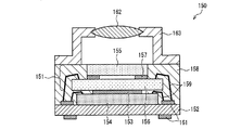
撮影装置50は、図7に示すように、固体撮像装置10、平板状の面と2つの凸面とからなる撮像用レンズ51、この撮像用レンズ51の平板状の面を挟んで形成された遮光部52、並びに撮像用レンズ51とセンサチップ2との光軸方向の距離を調節及び固定するためのスペーサ53を備えている。
As shown in FIG. 7, the
上記撮像用レンズ51は、固体撮像装置10に入射する光の光路を画定する光路画定器である。遮光部52は、撮像用レンズ51の絞りであり、かつ撮像用レンズ51に入射する光の内、迷光の入射を抑制する。スペーサ53は、封止樹脂5の外周部付近に形成されている。
The
尚、固体撮像装置10の底面に設けられた外部接続端子9は、図示しない配線基板上に形成された導体配線と電気的に接続されている。さらに、上記導体配線は、上記配線基板上に接着された図示しない画像処理装置に電気的に接続されている。つまり、撮影装置50は、上記導体配線を介して、上記画像処理装置と電気的に接続されている。
The external connection terminal 9 provided on the bottom surface of the solid-
このため、撮像用レンズ51から入射した光は、レンズ3、透明基板4、空気層7を介して、センサチップ2上の前記有効画素領域11に入射する。そして、有効画素領域11に入射した光は電気信号に変換され、上記画像処理装置に送信される。送信された電気信号に基づいて上記画像処理装置が画像を形成する。
Therefore, the light incident from the
本実施の形態の撮影装置50は、以上の構成を有しているので、固体撮像装置10と同様の機能及び作用を有する。
Since the
尚、撮影装置50は、固体撮像装置10の代わりに、固体撮像装置30又は固体撮像装置40を備えていてもよい。
Note that the
このように、本実施の形態の撮影装置50は、実施の形態1〜実施の形態3に記載の固体撮像装置10・30・40を備えている。
As described above, the
これにより、センサチップ2の周辺部への入射光が暗くなることを抑制し、かつセンサチップ2の有効画素領域へ入射する迷光を抑制し、さらに、高い信頼性を得ることができる固体撮像装置10・30・40を備えた撮影装置50を提供することができる。
Thereby, the solid-state imaging device which can suppress that the incident light to the peripheral part of the
尚、本発明は、上述した各実施形態に限定されるものではなく、請求項に示した範囲で種々の変更が可能であり、異なる実施形態にそれぞれ開示された技術的手段を適宜組み合わせて得られる実施形態についても本発明の技術的範囲に含まれる。 The present invention is not limited to the above-described embodiments, and various modifications can be made within the scope of the claims, and the technical means disclosed in different embodiments can be appropriately combined. Such embodiments are also included in the technical scope of the present invention.
本発明によれば、簡便で安価な方法を用いて小型化及び薄型化を達成し、かつ高い信頼性(耐環境性)及び性能を付与した固体撮像装置を提供することができるので、被写体からの光に基づいて画像を形成するための光学機器全般に適用可能である。特に、携帯電話用のカメラモジュールやデジタルカメラ等に適用することが有効である。装置の小型・薄型化かつ広角化の用途に利用することができる。 According to the present invention, it is possible to provide a solid-state imaging device that achieves downsizing and thinning using a simple and inexpensive method and that has high reliability (environment resistance) and performance. The present invention can be applied to all optical devices for forming an image based on the light of the above. In particular, it is effective to apply to a camera module for a mobile phone, a digital camera, or the like. It can be used for the purpose of downsizing, thinning and widening the device.
1 センサ基板
2 センサチップ(固体撮像素子)
3 レンズ(光学素子)
3’ 光硬化性樹脂(エネルギー硬化性樹脂)
3a レンズ角端部
3b レンズ辺端部
4 透明基板(透明板)
5 封止樹脂
6 スペーサ
7 空気層
8 ボンディングワイヤ
9 外部接続端子
10 固体撮像装置
11 有効画素領域
21 ロッド
22 成形型
23 カメラ
24 UVランプ
30 固体撮影装置
33 レンズ(光学素子)
40 固体撮像装置
41 有効画素領域
43 レンズ(光学素子)
50 撮影装置
51 撮像用レンズ
52 遮光部
53 スペーサ
SL1 直線
SL2 直線
CL 円
1
3 Lens (optical element)
3 'light curable resin (energy curable resin)
3a
DESCRIPTION OF
40 Solid-
50
Claims (18)
上記固体撮像素子の有効画素領域と対向するように配置された透明板と、
上記固体撮像素子の一部、及び上記透明板の側壁を封止する封止樹脂と、
透明な樹脂から構成された光学素子とを備え、
上記光学素子は、上記透明板上に形成され、かつ該光学素子の光軸方向から見たときに、該光学素子の外周は該透明板の外周よりも光軸中心側に形成されていることを特徴とする固体撮像装置。 A solid-state imaging device in which an effective pixel region is formed;
A transparent plate disposed so as to face the effective pixel region of the solid-state imaging device;
A sealing resin for sealing a part of the solid-state imaging device and a side wall of the transparent plate;
An optical element composed of a transparent resin,
The optical element is formed on the transparent plate, and the outer periphery of the optical element is formed closer to the optical axis center side than the outer periphery of the transparent plate when viewed from the optical axis direction of the optical element. A solid-state imaging device.
前記固体撮像素子の有効画素領域内に形成された有効領域と、それ以外の非有効領域とからなり、
上記光学素子の有効領域は、撮像系における有効光束を屈折させて上記固体撮像素子の有効画素領域に導く一方、
上記光学素子の非有効領域は、有効光束に関与しないように形成されていることを特徴とする請求項4,5又は6に記載の固体撮像装置。 The optical element is
The effective area formed in the effective pixel area of the solid-state imaging device, and other non-effective area,
The effective area of the optical element refracts an effective light beam in the imaging system and guides it to the effective pixel area of the solid-state imaging element,
7. The solid-state imaging device according to claim 4, wherein the ineffective area of the optical element is formed so as not to be involved in an effective light beam.
上記固体撮像素子の一部、及び上記透明板の側壁を封止樹脂により封止する第2の工程と、
上記透明板上に透明な樹脂から構成された光学素子を形成する第3の工程とを含み、
上記第3の工程において上記光学素子と上記封止樹脂とは接しないことを特徴とする固体撮像装置の製造方法。 A first step of disposing a transparent plate so as to face the effective pixel region of the solid-state image sensor and to be present inside the planar shape of the solid-state image sensor;
A second step of sealing a part of the solid-state imaging device and a side wall of the transparent plate with a sealing resin;
A third step of forming an optical element composed of a transparent resin on the transparent plate,
A method of manufacturing a solid-state imaging device, wherein the optical element and the sealing resin are not in contact with each other in the third step.
流動性を有するエネルギー硬化性樹脂を成形型に充填する第1の処理と、
光エネルギー又は熱エネルギーの付与によって上記エネルギー硬化性樹脂を硬化する第2の処理とを含むことを特徴とする請求項16に記載の固体撮像装置の製造方法。 The third step includes
A first treatment of filling a mold with an energy curable resin having fluidity;
The method for manufacturing a solid-state imaging device according to claim 16, further comprising: a second process for curing the energy curable resin by applying light energy or thermal energy.
Priority Applications (1)
| Application Number | Priority Date | Filing Date | Title |
|---|---|---|---|
| JP2007293698A JP2009123788A (en) | 2007-11-12 | 2007-11-12 | Solid-state imaging apparatus, method of manufacturing solid-state imaging apparatus, and photographic apparatus using the same solid-state imaging apparatus |
Applications Claiming Priority (1)
| Application Number | Priority Date | Filing Date | Title |
|---|---|---|---|
| JP2007293698A JP2009123788A (en) | 2007-11-12 | 2007-11-12 | Solid-state imaging apparatus, method of manufacturing solid-state imaging apparatus, and photographic apparatus using the same solid-state imaging apparatus |
Publications (1)
| Publication Number | Publication Date |
|---|---|
| JP2009123788A true JP2009123788A (en) | 2009-06-04 |
Family
ID=40815653
Family Applications (1)
| Application Number | Title | Priority Date | Filing Date |
|---|---|---|---|
| JP2007293698A Pending JP2009123788A (en) | 2007-11-12 | 2007-11-12 | Solid-state imaging apparatus, method of manufacturing solid-state imaging apparatus, and photographic apparatus using the same solid-state imaging apparatus |
Country Status (1)
| Country | Link |
|---|---|
| JP (1) | JP2009123788A (en) |
Cited By (6)
| Publication number | Priority date | Publication date | Assignee | Title |
|---|---|---|---|---|
| JP2019008253A (en) * | 2017-06-28 | 2019-01-17 | 京セラ株式会社 | Imaging device and moving body |
| WO2019131488A1 (en) * | 2017-12-28 | 2019-07-04 | ソニーセミコンダクタソリューションズ株式会社 | Camera package, camera package production method, and electronic device |
| WO2020039958A1 (en) * | 2018-08-22 | 2020-02-27 | ソニーセミコンダクタソリューションズ株式会社 | Solid-state imaging device, imaging device, and electronic equipment |
| WO2020171037A1 (en) * | 2019-02-22 | 2020-08-27 | ソニーセミコンダクタソリューションズ株式会社 | Camera package, method of manufacturing camera package, and electronic equipment |
| WO2021095562A1 (en) * | 2019-11-13 | 2021-05-20 | ソニーセミコンダクタソリューションズ株式会社 | Imaging device and electronic instrument |
| CN113192994A (en) * | 2021-05-07 | 2021-07-30 | 豪威光电子科技(上海)有限公司 | Lens module and forming method thereof |
-
2007
- 2007-11-12 JP JP2007293698A patent/JP2009123788A/en active Pending
Cited By (12)
| Publication number | Priority date | Publication date | Assignee | Title |
|---|---|---|---|---|
| JP2019008253A (en) * | 2017-06-28 | 2019-01-17 | 京セラ株式会社 | Imaging device and moving body |
| WO2019131488A1 (en) * | 2017-12-28 | 2019-07-04 | ソニーセミコンダクタソリューションズ株式会社 | Camera package, camera package production method, and electronic device |
| JPWO2019131488A1 (en) * | 2017-12-28 | 2021-01-21 | ソニーセミコンダクタソリューションズ株式会社 | Camera packages, camera package manufacturing methods, and electronic devices |
| US11574949B2 (en) | 2017-12-28 | 2023-02-07 | Sony Semiconductor Solutions Corporation | Camera package, manufacturing method of camera package, and electronic device |
| JP7379163B2 (en) | 2017-12-28 | 2023-11-14 | ソニーセミコンダクタソリューションズ株式会社 | Camera package, camera package manufacturing method, and electronic equipment |
| WO2020039958A1 (en) * | 2018-08-22 | 2020-02-27 | ソニーセミコンダクタソリューションズ株式会社 | Solid-state imaging device, imaging device, and electronic equipment |
| US11728363B2 (en) | 2018-08-22 | 2023-08-15 | Sony Semiconductor Solutions Corporation | Solid-state imaging device, imaging device, and electronic apparatus |
| WO2020171037A1 (en) * | 2019-02-22 | 2020-08-27 | ソニーセミコンダクタソリューションズ株式会社 | Camera package, method of manufacturing camera package, and electronic equipment |
| CN113348064A (en) * | 2019-02-22 | 2021-09-03 | 索尼半导体解决方案公司 | Camera package, method of manufacturing camera package, and electronic apparatus |
| EP3928946A4 (en) * | 2019-02-22 | 2022-03-23 | Sony Semiconductor Solutions Corporation | Camera package, method of manufacturing camera package, and electronic equipment |
| WO2021095562A1 (en) * | 2019-11-13 | 2021-05-20 | ソニーセミコンダクタソリューションズ株式会社 | Imaging device and electronic instrument |
| CN113192994A (en) * | 2021-05-07 | 2021-07-30 | 豪威光电子科技(上海)有限公司 | Lens module and forming method thereof |
Similar Documents
| Publication | Publication Date | Title |
|---|---|---|
| JP4686400B2 (en) | Optical device, optical device apparatus, camera module, and optical device manufacturing method | |
| JP4694602B2 (en) | Solid-state imaging device and electronic apparatus including the same | |
| KR100575094B1 (en) | Module for optical device, and manufacturing method therefor | |
| TWI392337B (en) | Wafer based camera module and method of manufacture | |
| JP5009209B2 (en) | Wafer-like optical device and manufacturing method thereof, electronic element wafer module, sensor wafer module, electronic element module, sensor module, and electronic information device | |
| JP2012222546A (en) | Solid-state imaging device, method for manufacturing the same, and electronic apparatus | |
| KR100730726B1 (en) | Camera module | |
| CN101271913B (en) | Optical device, camera module, mobile phone, digital still camera, and medical endoscope | |
| KR20060056870A (en) | Image pickup module and manufacturing method of image pickup module | |
| JP2007158751A (en) | Imaging apparatus and its manufacturing method | |
| JP2005020687A (en) | Imaging device and its manufacturing method | |
| JP2007027713A (en) | Manufacturing method of optical device to which transparent cover is attached and manufacturing method of optical device module using the same | |
| JP2009123788A (en) | Solid-state imaging apparatus, method of manufacturing solid-state imaging apparatus, and photographic apparatus using the same solid-state imaging apparatus | |
| JP4153016B1 (en) | Solid-state imaging device, method for manufacturing solid-state imaging device, and imaging device using the solid-state imaging device | |
| JP2005317745A (en) | Solid-state imaging apparatus and method for manufacturing the same | |
| JP4248586B2 (en) | IMAGING DEVICE, MANUFACTURING METHOD THEREOF, AND PORTABLE INFORMATION TERMINAL AND IMAGING DEVICE WITH THE IMAGING DEVICE | |
| JP2009171065A (en) | Solid imaging apparatus, method for manufacturing solid imaging apparatus and photographing device using solid imaging apparatus | |
| JP4324633B2 (en) | SOLID-STATE IMAGING DEVICE, MANUFACTURING METHOD THEREOF, AND PHOTOGRAPHING DEVICE HAVING THE SOLID-STATE IMAGING DEVICE | |
| JP2017208468A (en) | Electronic component | |
| JPWO2003015400A1 (en) | The camera module | |
| US20100321563A1 (en) | Solid-state imaging unit | |
| JP2006080597A (en) | Image pickup module and method of manufacturing the same | |
| WO2019198318A1 (en) | Imaging device, electronic apparatus, and method for manufacturing imaging device | |
| JP2008289096A (en) | Solid-state imaging module, imaging apparatus, imaging equipment, and method of manufacturing solid-state imaging module | |
| JP2004096638A (en) | Imaging device and manufacturing method therefor |