EP3575438B1 - Cu-ga-legierungs-sputtertarget und verfahren zur herstellung des cu-ga-legierungs-sputtertargets - Google Patents
Cu-ga-legierungs-sputtertarget und verfahren zur herstellung des cu-ga-legierungs-sputtertargets Download PDFInfo
- Publication number
- EP3575438B1 EP3575438B1 EP18892002.9A EP18892002A EP3575438B1 EP 3575438 B1 EP3575438 B1 EP 3575438B1 EP 18892002 A EP18892002 A EP 18892002A EP 3575438 B1 EP3575438 B1 EP 3575438B1
- Authority
- EP
- European Patent Office
- Prior art keywords
- sputtering target
- complex fluorides
- alloy
- powder
- alloy sputtering
- Prior art date
- Legal status (The legal status is an assumption and is not a legal conclusion. Google has not performed a legal analysis and makes no representation as to the accuracy of the status listed.)
- Active
Links
Images




Classifications
-
- C—CHEMISTRY; METALLURGY
- C23—COATING METALLIC MATERIAL; COATING MATERIAL WITH METALLIC MATERIAL; CHEMICAL SURFACE TREATMENT; DIFFUSION TREATMENT OF METALLIC MATERIAL; COATING BY VACUUM EVAPORATION, BY SPUTTERING, BY ION IMPLANTATION OR BY CHEMICAL VAPOUR DEPOSITION, IN GENERAL; INHIBITING CORROSION OF METALLIC MATERIAL OR INCRUSTATION IN GENERAL
- C23C—COATING METALLIC MATERIAL; COATING MATERIAL WITH METALLIC MATERIAL; SURFACE TREATMENT OF METALLIC MATERIAL BY DIFFUSION INTO THE SURFACE, BY CHEMICAL CONVERSION OR SUBSTITUTION; COATING BY VACUUM EVAPORATION, BY SPUTTERING, BY ION IMPLANTATION OR BY CHEMICAL VAPOUR DEPOSITION, IN GENERAL
- C23C14/00—Coating by vacuum evaporation, by sputtering or by ion implantation of the coating forming material
- C23C14/22—Coating by vacuum evaporation, by sputtering or by ion implantation of the coating forming material characterised by the process of coating
- C23C14/34—Sputtering
- C23C14/3407—Cathode assembly for sputtering apparatus, e.g. Target
- C23C14/3414—Metallurgical or chemical aspects of target preparation, e.g. casting, powder metallurgy
-
- C—CHEMISTRY; METALLURGY
- C22—METALLURGY; FERROUS OR NON-FERROUS ALLOYS; TREATMENT OF ALLOYS OR NON-FERROUS METALS
- C22C—ALLOYS
- C22C9/00—Alloys based on copper
-
- C—CHEMISTRY; METALLURGY
- C23—COATING METALLIC MATERIAL; COATING MATERIAL WITH METALLIC MATERIAL; CHEMICAL SURFACE TREATMENT; DIFFUSION TREATMENT OF METALLIC MATERIAL; COATING BY VACUUM EVAPORATION, BY SPUTTERING, BY ION IMPLANTATION OR BY CHEMICAL VAPOUR DEPOSITION, IN GENERAL; INHIBITING CORROSION OF METALLIC MATERIAL OR INCRUSTATION IN GENERAL
- C23C—COATING METALLIC MATERIAL; COATING MATERIAL WITH METALLIC MATERIAL; SURFACE TREATMENT OF METALLIC MATERIAL BY DIFFUSION INTO THE SURFACE, BY CHEMICAL CONVERSION OR SUBSTITUTION; COATING BY VACUUM EVAPORATION, BY SPUTTERING, BY ION IMPLANTATION OR BY CHEMICAL VAPOUR DEPOSITION, IN GENERAL
- C23C14/00—Coating by vacuum evaporation, by sputtering or by ion implantation of the coating forming material
- C23C14/22—Coating by vacuum evaporation, by sputtering or by ion implantation of the coating forming material characterised by the process of coating
- C23C14/34—Sputtering
-
- H—ELECTRICITY
- H10—SEMICONDUCTOR DEVICES; ELECTRIC SOLID-STATE DEVICES NOT OTHERWISE PROVIDED FOR
- H10F—INORGANIC SEMICONDUCTOR DEVICES SENSITIVE TO INFRARED RADIATION, LIGHT, ELECTROMAGNETIC RADIATION OF SHORTER WAVELENGTH OR CORPUSCULAR RADIATION
- H10F10/00—Individual photovoltaic cells, e.g. solar cells
- H10F10/10—Individual photovoltaic cells, e.g. solar cells having potential barriers
- H10F10/16—Photovoltaic cells having only PN heterojunction potential barriers
- H10F10/167—Photovoltaic cells having only PN heterojunction potential barriers comprising Group I-III-VI materials, e.g. CdS/CuInSe2 [CIS] heterojunction photovoltaic cells
-
- B—PERFORMING OPERATIONS; TRANSPORTING
- B22—CASTING; POWDER METALLURGY
- B22F—WORKING METALLIC POWDER; MANUFACTURE OF ARTICLES FROM METALLIC POWDER; MAKING METALLIC POWDER; APPARATUS OR DEVICES SPECIALLY ADAPTED FOR METALLIC POWDER
- B22F2998/00—Supplementary information concerning processes or compositions relating to powder metallurgy
- B22F2998/10—Processes characterised by the sequence of their steps
-
- B—PERFORMING OPERATIONS; TRANSPORTING
- B22—CASTING; POWDER METALLURGY
- B22F—WORKING METALLIC POWDER; MANUFACTURE OF ARTICLES FROM METALLIC POWDER; MAKING METALLIC POWDER; APPARATUS OR DEVICES SPECIALLY ADAPTED FOR METALLIC POWDER
- B22F2999/00—Aspects linked to processes or compositions used in powder metallurgy
-
- Y—GENERAL TAGGING OF NEW TECHNOLOGICAL DEVELOPMENTS; GENERAL TAGGING OF CROSS-SECTIONAL TECHNOLOGIES SPANNING OVER SEVERAL SECTIONS OF THE IPC; TECHNICAL SUBJECTS COVERED BY FORMER USPC CROSS-REFERENCE ART COLLECTIONS [XRACs] AND DIGESTS
- Y02—TECHNOLOGIES OR APPLICATIONS FOR MITIGATION OR ADAPTATION AGAINST CLIMATE CHANGE
- Y02E—REDUCTION OF GREENHOUSE GAS [GHG] EMISSIONS, RELATED TO ENERGY GENERATION, TRANSMISSION OR DISTRIBUTION
- Y02E10/00—Energy generation through renewable energy sources
- Y02E10/50—Photovoltaic [PV] energy
- Y02E10/541—CuInSe2 material PV cells
-
- Y—GENERAL TAGGING OF NEW TECHNOLOGICAL DEVELOPMENTS; GENERAL TAGGING OF CROSS-SECTIONAL TECHNOLOGIES SPANNING OVER SEVERAL SECTIONS OF THE IPC; TECHNICAL SUBJECTS COVERED BY FORMER USPC CROSS-REFERENCE ART COLLECTIONS [XRACs] AND DIGESTS
- Y02—TECHNOLOGIES OR APPLICATIONS FOR MITIGATION OR ADAPTATION AGAINST CLIMATE CHANGE
- Y02P—CLIMATE CHANGE MITIGATION TECHNOLOGIES IN THE PRODUCTION OR PROCESSING OF GOODS
- Y02P70/00—Climate change mitigation technologies in the production process for final industrial or consumer products
- Y02P70/50—Manufacturing or production processes characterised by the final manufactured product
Definitions
- the present invention relates to a Cu-Ga alloy sputtering target, for example, used when forming a Cu-In-Ga-Se compound film (hereinafter abbreviated as a CIGS film) to be a light absorption layer of a CIGS solar cell, and a method of manufacturing the Cu-Ga alloy sputtering target.
- a Cu-Ga alloy sputtering target for example, used when forming a Cu-In-Ga-Se compound film (hereinafter abbreviated as a CIGS film) to be a light absorption layer of a CIGS solar cell, and a method of manufacturing the Cu-Ga alloy sputtering target.
- a CIGS solar cell including a light absorption layer formed of a CIGS film is provided.
- a deposition method using a vapor deposition method is known.
- a solar cell including the light absorption layer deposited by the vapor deposition method has an advantage that an energy exchange efficiency is high.
- uniformity in film thickness distribution was likely to be deteriorated.
- an In film is deposited using an In sputtering target
- a Cu-Ga film is deposited on the In film by using a Cu-Ga sputtering target, and a laminated film of the In film and the Cu-Ga film is formed.
- the CIGS film is formed by heat treating the laminated film in a Se atmosphere and selenizing the laminated film.
- NPL 1 it is known that when an alkali metal such as Na or K, is added to a CIGS film to be a light absorption layer, the conversion efficiency of a solar cell is improved.
- PTL 1 discloses that Na is added to a Cu-Ga alloy sputtering target used when a Cu-Ga film is deposited
- PTL 2 proposes that K is added to a Cu-Ga alloy sputtering target used when a Cu-Ga film is deposited.
- PTL 3 relates to a sputtering target having a composition containing 5-60 atom% of Ga and 0.01-5 atom% of an alkali metal as metal components, the balance being Cu and unavoidable impurities, wherein the alkali metal concentration of the surface on the sputtering-surface side is less than 80% of the alkali metal concentration of the target interior.
- Potassium fluoride (KF) has a hygroscopic property lower than that of selenides and sulfides, but has a property in that it relatively easily absorbs moisture.
- KF potassium fluoride
- the sputtering target is stored in an atmosphere, moisture in the air is absorbed, and a surface of the sputtering target is oxidized and discolored. Therefore, there was a problem that a defect such as abnormal discharge during sputtering might occur. Therefore, it is necessary to store the sputtering target strictly, and there was a problem that process management in manufacturing a solar cell might be greatly hindered.
- An object of the present invention is to provide a Cu-Ga alloy sputtering target in which Na and K are included, discoloration is suppressed even when stored in an atmosphere, and stable sputtering deposition is possible, and to provide a method of manufacturing the Cu-Ga alloy sputtering target.
- a Cu-Ga alloy sputtering target having a composition comprising: as a metal component, Ga in a range of 20 at% or more and 45 at% or less; K and Na in a range of 0.1 at% or more and 2 at% or less in total; and a Cu balance including inevitable impurities, in which, complex fluorides containing Na, K, and F are dispersed in a matrix of a Cu-Ga alloy, a maximum diameter of an inscribed circle of the complex fluorides is 30 ⁇ m or less, and [Na]/([Na]+[K]) is set to be in a range of 0.3 or more and 0.9 or less, [Na] and [K] being atomic ratios of Na and K in the complex fluorides, respectively.
- the complex fluorides containing Na, K, and F is dispersed. Therefore, it is possible to deposit a Cu-Ga alloy film containing Na and K.
- the complex fluoride is an insulator, when the maximum diameter of the inscribed circle of the complex fluorides is set to 30 ⁇ m or less, abnormal discharge caused by the complex fluorides can be prevented from occurring.
- an oxygen concentration is set to 1000 mass ppm or less.
- the oxygen concentration is limited to 1000 mass ppm or less, the complex fluorides containing Na, K, and F can be prevented from reacting with oxygen to form a sodium oxide and a potassium oxide having high hygroscopic properties.
- abnormal discharge at the time of sputtering deposition can be prevented from occurring.
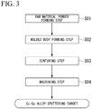
- a method of manufacturing the Cu-Ga alloy sputtering target described above includes the steps of: a raw material powder forming step of mixing a pure Cu powder, a Cu-Ga alloy powder, and a complex fluorides powder formed of a complex fluorides containing Na, K, and F to obtain a raw material powder; a molded body forming step of forming a molded body of the raw material powder; and a sintering step of heating the molded body in a reducing atmosphere to perform pressureless sintering.
- the complex fluorides powder formed of the complex fluorides containing Na, K, and F can be prevented from containing an excessive amount of water due to moisture absorption. Accordingly, at the time of sintering, it can be prevented that the surface of the raw material powder is oxidized by the moisture to inhibit sinterability, and the sinterability can be improved.
- the liquid phase can be prevented from leaking out of the molded body, and the sintering can be favorably performed.
- the present invention it is possible to provide a Cu-Ga alloy sputtering target in which Na and K are contained, and even when stored in an atmosphere, discoloration is suppressed, and stable sputtering deposition is possible, and a method of manufacturing the Cu-Ga alloy sputtering target.
- the Cu-Ga alloy sputtering target according to the present embodiment is used when depositing a Cu-Ga film by sputtering, in order to form a light absorption layer formed of a CIGS film in a CIGS thin film solar cell.
- the Cu-Ga alloy sputtering target according to the present embodiment having a composition comprising: as a metal component, Ga in a range of 20 at% or more and 45 at% or less; K and Na in a range of 0.1 at% or more and 2 at% or less in total; and a Cu balance including inevitable impurities.
- a disk-shaped sputtering target having a circular sputtering surface is used.
- the complex fluorides containing Na, K, and F is dispersed and a maximum diameter of an inscribed circle of the complex fluorides is set to 30 ⁇ m or less.
- [Na]/([Na]+[K]) is set to be in a range of 0.3 or more and 0.9 or less, [Na] and [K] being atomic ratios of Na and K in the complex fluorides, respectively.
- the oxygen concentration is set to 1000 mass ppm or less.
- the relative density is set to 90% or higher.
- the alkali salt in a case where the total content of K and Na exceeds 2 at%, the alkali salt is excessively contained. Accordingly, the hygroscopic property cannot be suppressed to be low. In addition, there was a concern that the surface of the sputtering target might be oxidized and discolored when stored in the atmosphere.
- the total content of K and Na is set to be in the range of 0.1 at% or more and 2 at% or less.
- a lower limit of the total content of K and Na is preferably 0.2 at% or more, and more preferably 0.3 at% or more.
- an upper limit of the total content of K and Na is preferably 1.5 at% or less, and more preferably 1.2 at% or less.
- the complex fluorides containing Na, K, and F has hygroscopic property lower than that of the potassium fluoride (KF), even when stored in the atmosphere, the surface of the sputtering target can be prevented from oxidizing and discoloring.
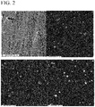
- the complex fluorides containing Na, K, and F can be confirmed when in an element mapping image obtained by a wavelength separation type X-ray detector of an electron probe micro analyzer (EPMA), there is a region where Na, K, and F coexist in a substrate of the Cu-Ga alloy.
- EPMA electron probe micro analyzer
- the complex fluorides containing Na, K, and F described above is an insulator. Therefore, when a particle diameter of the complex fluorides is large, abnormal discharge is likely to occur at the time of sputtering deposition.
- the maximum diameter of the inscribed circle of the complex fluorides containing Na, K, and F is limited to 30 ⁇ m or less.
- samples were taken from 5 sites of a center (1) of the circle that the sputtering surface forms, and outer peripheral portions (2), (3), (4), and (5), on two straight lines which pass through the center of the circle and orthogonal to each other.
- a tissue of the samples was observed at a magnification of 360 times. The observation was performed in 3 fields of view for one sample, and the maximum diameter of the inscribed circle of the complex fluorides was measured in 15 fields of view in total.
- the maximum diameter of the inscribed circle of the complex fluorides containing Na, K, and F is preferably set to 30 ⁇ m or less, and more preferably set to 20 ⁇ m or less.
- [Na]/([Na]+[K]) is set to be in a range of 0.3 or more, [Na] and [K] being atomic ratios of Na and K in the complex fluorides, respectively. Accordingly, a proportion of Na in the complex fluorides is secured.
- [Na]/([Na]+[K]) is set to be in a range of 0.9 or less, [Na] and [K] being atomic ratios of Na and K in the complex fluorides, respectively.
- a lower limit of [Na]/([Na]+[K]) is preferably 0.35 or more, and more preferably 0.45 or more.
- an upper limit of [Na]/([Na]+[K]) is preferably 0.8 or less, and more preferably 0.7 or less.
- the oxygen concentration in the Cu-Ga alloy sputtering target is limited to 1000 mass ppm or less. Accordingly, formation of the sodium oxide or the potassium oxide having high hygroscopic property is suppressed.
- the oxygen concentration in the Cu-Ga alloy sputtering target is preferably 900 mass ppm or less, and more preferably 800 mass ppm or less.
- the relative density is set to 90% or more. Accordingly, the number of voids in the Cu-Ga alloy sputtering target can be reduced, and the abnormal discharge at the time of sputtering deposition can be prevented from occurring.
- the relative density of the Cu-Ga alloy sputtering target is preferably 93% or higher, and more preferably 95% or higher.
- a pure copper powder, a Cu-Ga alloy powder, and a complex fluorides powder formed of the complex fluorides containing Na, K, and F are prepared.
- a median diameter D50 measured by micro track is 2 to 3 ⁇ m.
- the Cu-Ga alloy powder is manufactured by an atomization method, and a median diameter D50 measured by micro track is 20 to 30 ⁇ m.
- a Ga content is set to be in a range of 45 at% or more and 49 at% or less.
- the complex fluorides powder formed of the complex fluorides containing Na, K, and F was manufactured as follows.
- NaF and KF are weighed to have a predetermined composition, and heated and melted in an inert gas atmosphere to manufacture a mass of the complex fluorides containing Na, K, and F.
- NaF and KF undergo eutectic reaction as shown in FIG. 4 .
- the resulting mass of the complex fluorides is pulverized and sieved to have a maximum particle size of 20 ⁇ m or less, and the complex fluorides powder described above was obtained.
- the pure copper powder, the Cu-Ga alloy powder, and the complex fluorides powder described above are weighed to have a predetermined composition, and mixed in an inert atmosphere (Ar atmosphere) using a mixing apparatus such as a Henschel mixer to obtain the raw material powder.
- a mixing apparatus such as a Henschel mixer
- the pure copper powder is contained in a range of 3 mol% or more and 60 mol% or less of a whole raw material powder.
- a green compact (a molded body) was formed using the raw material powder obtained as described above, at 500 kgf/cm 2 to 2000 kgf/cm 2 of molding pressure.
- the molded body obtained as described above is charged into a sintering furnace, heated in a pressureless state at a temperature rising rate of 10°C/min to reach a predetermined sintering temperature, while flowing a reducing gas such as hydrogen, carbon monoxide, and ammonia decomposition gas in a range of 10 L/min or more and 100 L/min or less, and held at the sintering temperature for 5 hours. Then, it was naturally cooled in the sintering furnace to obtain a sintered material.
- a reducing gas such as hydrogen, carbon monoxide, and ammonia decomposition gas
- the sintering temperature is set according to the Ga content in the Cu-Ga alloy powder.
- the sintered material described above is machined on a lathe to obtain a Cu-Ga alloy sputtering target having a predetermined size.
- the Cu-Ga alloy sputtering target according to the present embodiment is manufactured.
- the complex fluorides containing Na, K, and F is dispersed in the matrix of the Cu-Ga alloy. Therefore, it is possible to deposit the Cu-Ga alloy film containing Na and K by sputtering deposition using the Cu-Ga alloy sputtering target. Accordingly, a solar cell having high conversion efficiency can be configured.
- the hygroscopic property is sufficiently lower than that of the potassium fluoride (KF), and even when stored in the atmosphere, the surface of the Cu-Ga alloy sputtering target can be prevented from oxidizing and discoloring.
- the maximum diameter of the inscribed circle of the complex fluorides, which is an insulator is limited to 30 ⁇ m or less, at the time of sputtering deposition, abnormal discharge caused by the complex fluorides can be prevented from occurring.
- [Na]/([Na]+[K]) is set to be in a range of 0.3 or more, [Na] and [K] being atomic ratios of Na and K in the complex fluorides, respectively. Therefore, a proportion of Na in the complex fluorides is secured. And it is possible to suppress the hygroscopic property of the complex fluorides surely to be low and further prevent the Cu-Ga alloy sputtering target from discoloring.
- [Na]/([Na]+[K]) is set to be in a range of 0.9 or less, [Na] and [K] being atomic ratios of Na and K in the complex fluorides, respectively. Therefore, a proportion of K in the complex fluorides is secured. And it is possible to deposit the Cu-Ga alloy film containing Na and K and form a solar cell with high conversion efficiency.
- the complex fluorides containing Na, K, and F can be prevented from reacting with oxygen to form a sodium oxide and a potassium oxide having high hygroscopic property, and it is possible to further prevent the Cu-Ga alloy sputtering target from discoloring.
- abnormal discharge caused by the oxide described above can be prevented from occurring.
- the relative density is set to 90% or more. Therefore, the number of voids in the Cu-Ga alloy sputtering target can be reduced, and the abnormal discharge at the time of sputtering deposition can be prevented from occurring.
- the complex fluorides powder formed of the complex fluorides containing Na, K, and F is used as the raw material powder, and the raw material powder can be prevented from containing an excessive amount of water due to moisture absorption. Accordingly, at the time of sintering, the surface of the raw material powder can be prevented from being oxidized by the moisture to inhibit sinterability, and the sinterability can be improved.
- the pure Cu powder which is likely to be plastically deformed is used as the raw material powder. Therefore, in the molded body forming step S02, a shape of the molded body can be easily maintained.
- the Cu-Ga alloy powder is used as the raw material powder. Therefore, the relative density of the sintered material can be increased by adjusting the sintering temperature according to the Ga content of the Cu-Ga alloy powder.
- the pressureless sintering is performed in the sintering step S03, the formed liquid phase can be prevented from leaking out of the molded body, and the sintering can be favorably performed.
- a rectangular flat sputtering target having a rectangular sputtering surface may be used.
- a cylindrical-shaped sputtering target having a cylindrical sputtering surface may also be used.
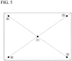
- samples were taken from 5 sites of an intersection (1) where diagonals intersect to each other and corners (2), (3), (4), and (5) on each diagonal, a tissue of the samples was observed at a magnification of 360 times, the observation was performed in 3 fields of view for one sample, and the maximum diameter of the inscribed circle of the complex fluorides was measured in 15 fields of view in total.
- samples were taken from 4 sites, (1), (2), (3), and (4), at equal intervals (90° intervals) in a circumferential direction in the center portion of an axial direction, a tissue of the samples was observed at a magnification of 360 times, the observation was performed in 3 fields of view for one sample, and the maximum diameter of the inscribed circle of the complex fluorides was measured in 12 fields of view in total.
- a complex fluorides formed of a pure copper powder (a median diameter: 3 ⁇ m, purity: 99.9 mass% or more), a Cu-Ga alloy atomized powder (median diameter: 25 ⁇ m) having a composition shown in Table 1, and a complex fluorides containing Na, K, and F having a composition shown in Table 1 was prepared.
- a NaF powder (median diameter 8 ⁇ m) and KF powder (median diameter 5 ⁇ m) to be used as comparative examples were prepared.
- the pure copper powder, the Cu-Ga alloy atomized powder, the complex fluorides powder, NaF powder, and KF powder described above were weighed to satisfy a mixing ratio shown in Table 2, and mixed in an Ar atmosphere using a Henschel mixer to obtain the raw material powder.
- a mold is filled with the raw material powder described above and pressed at a molding pressure of 1000 kgf/cm 2 to obtain a disc-shaped molded body.
- the molded body was placed in a firing furnace and sintered under conditions shown in Table 2.
- the temperature rising rate is set to 10°C/min to reach a sintering temperature.
- the sintering temperature was kept for 5 hours, and then naturally cooled in the furnace. Accordingly, the sintered material was obtained.
- the resulting sintered material was machined to manufacture a disc-shaped Cu-Ga alloy sputtering target having a diameter of 125 mm and a thickness of 6 mm.
- the prepared Cu-Ga alloy sputtering target was pulverized and pretreated with acid. Then, a composition analysis of Ga, K, and Na was performed by ICP-AES. The Cu component was described as a balance excluding Ga, K, and Na.
- the complex fluorides containing Na, K, and F was confirmed when in an element mapping image obtained by a wavelength separation type X-ray detector of an electron probe micro analyzer (EPMA: JXA-8530F manufactured by JEOL Ltd.), there is a region where Na, K, and F coexist in a substrate of the Cu-Ga alloy.
- EPMA electron probe micro analyzer
- samples were taken from 5 sites of a center (1) of the circle, and outer peripheral portions (2), (3), (4), and (5), on two straight lines which pass through the center of the circle and orthogonal to each other.
- a tissue of the samples was observed at a magnification of 360 times. The observation was performed in 3 fields of view for one sample, and the maximum diameter of the inscribed circle of the complex fluorides was measured in 15 fields of view in total.
- the atomic ratio [Na] of Na and the atomic ratio [K] of K in the complex fluorides were observed at an accelerating voltage of 15 kV using an electron probe micro analyzer (EPMA: JXA-8530F manufactured by JEOL Ltd.).
- the compositional analysis of the exposed complex fluorides was carried out by ion processing the section of the samples to measure a content of K and Na in the complex fluorides.
- contents of K and Na in the complex fluorides were measured in a total of 15 fields of view, and an average value of these was determined.
- the prepared Cu-Ga alloy sputtering target was soldered to a backing plate made of Cu using In solder. Then, sputtering deposition was performed under the following conditions, and the number of occurrences of abnormal discharge was measured. In order to remove a surface defect of the Cu-Ga alloy sputtering target, pre-sputtering was carried out under the following conditions. Thereafter, the number of abnormal discharges was measured.
- the present invention it is possible to provide a Cu-Ga alloy sputtering target in which Na and K are contained, and even when stored in an atmosphere, discoloration is suppressed, and stable sputtering deposition is possible, and a method of manufacturing the Cu-Ga alloy sputtering target.
Landscapes
- Chemical & Material Sciences (AREA)
- Engineering & Computer Science (AREA)
- Materials Engineering (AREA)
- Mechanical Engineering (AREA)
- Metallurgy (AREA)
- Organic Chemistry (AREA)
- Chemical Kinetics & Catalysis (AREA)
- Physical Vapour Deposition (AREA)
- Photovoltaic Devices (AREA)
- Powder Metallurgy (AREA)
Claims (3)
- Cu-Ga-Legierungs-Sputtertarget mit einer Zusammensetzung, die folgendes umfasst: Ga in einem Bereich von 20 At.-% oder mehr und 45 At.-% oder weniger als eine Metallkomponente; K und Na in einem Bereich von 0,1 At.-% oder mehr und 2 At.-% oder weniger insgesamt; und einen Cu-Rest einschließlich unvermeidbarer Verunreinigungen, wobeikomplexe Fluoride, die Na, K und F enthalten, in einer Matrix einer Cu-Ga-Legierung dispergiert sind,ein maximaler Inkreis-Durchmesser der komplexen Fluoride 30 µm oder weniger beträgt, und[Na]/([Na]+[K]) auf einen Bereich von 0,3 oder mehr und 0,9 oder weniger eingestellt ist, wobei [Na] und [K] Atomverhältnisse von Na bzw. K in den komplexen Fluoriden sind.
- Cu-Ga-Legierungs-Sputtertarget gemäß Anspruch 1, wobei eine Sauerstoffkonzentration auf 1000 Massen-ppm oder weniger eingestellt ist.
- Verfahren zur Herstellung des Cu-Ga-Legierungs-Sputtertargets gemäß Anspruch 1 oder 2, wobei das Verfahren die folgenden Schritte umfasst:einen Rohmaterialpulver-Bildungsschritt, in dem ein reines Cu-Pulver, ein Cu-Ga-Legierungspulver und ein Pulver aus komplexen Fluoriden, die Na, K und F enthalten, so gemischt werden, dass ein Rohmaterialpulver erhalten wird;einen Formkörper-Bildungsschritt, in dem ein Formkörper aus dem Rohmaterialpulver gebildet wird; undeinen Sinterschritt, in dem der Formkörper so in einer reduzierenden Atmosphäre erwärmt wird, dass druckloses Sintern durchgeführt wird.
Applications Claiming Priority (2)
| Application Number | Priority Date | Filing Date | Title |
|---|---|---|---|
| JP2017246339A JP6531816B1 (ja) | 2017-12-22 | 2017-12-22 | Cu−Ga合金スパッタリングターゲット、及び、Cu−Ga合金スパッタリングターゲットの製造方法 |
| PCT/JP2018/046750 WO2019124430A1 (ja) | 2017-12-22 | 2018-12-19 | Cu-Ga合金スパッタリングターゲット、及び、Cu-Ga合金スパッタリングターゲットの製造方法 |
Publications (3)
| Publication Number | Publication Date |
|---|---|
| EP3575438A1 EP3575438A1 (de) | 2019-12-04 |
| EP3575438A4 EP3575438A4 (de) | 2020-02-26 |
| EP3575438B1 true EP3575438B1 (de) | 2021-11-10 |
Family
ID=66934294
Family Applications (1)
| Application Number | Title | Priority Date | Filing Date |
|---|---|---|---|
| EP18892002.9A Active EP3575438B1 (de) | 2017-12-22 | 2018-12-19 | Cu-ga-legierungs-sputtertarget und verfahren zur herstellung des cu-ga-legierungs-sputtertargets |
Country Status (5)
| Country | Link |
|---|---|
| EP (1) | EP3575438B1 (de) |
| JP (1) | JP6531816B1 (de) |
| CN (1) | CN110337508B (de) |
| TW (1) | TWI687521B (de) |
| WO (1) | WO2019124430A1 (de) |
Family Cites Families (13)
| Publication number | Priority date | Publication date | Assignee | Title |
|---|---|---|---|---|
| WO2009081157A1 (en) * | 2007-12-24 | 2009-07-02 | Foseco International Limited | Improved modifying flux for molten aluminium |
| WO2011083647A1 (ja) * | 2010-01-07 | 2011-07-14 | Jx日鉱日石金属株式会社 | Cu-Ga系スパッタリングターゲット、同ターゲットの製造方法、光吸収層及び該光吸収層を用いた太陽電池 |
| US9410259B2 (en) * | 2011-09-02 | 2016-08-09 | Alliance For Sustainable Energy, Llc | Electrodeposition of gallium for photovoltaics |
| US20130168825A1 (en) * | 2011-12-30 | 2013-07-04 | Alliance For Sustainable Energy, Llc | Fabrication of ionic liquid electrodeposited cu-sn-zn-s-se thin films and method of making |
| KR20150023925A (ko) * | 2012-11-13 | 2015-03-05 | 제이엑스 닛코 닛세키 킨조쿠 가부시키가이샤 | Cu-Ga 합금 스퍼터링 타깃 및 그 제조 방법 |
| JP5594618B1 (ja) * | 2013-02-25 | 2014-09-24 | 三菱マテリアル株式会社 | スパッタリングターゲット及びその製造方法 |
| JP6120076B2 (ja) | 2013-08-01 | 2017-04-26 | 三菱マテリアル株式会社 | Cu−Ga合金スパッタリングターゲット及びその製造方法 |
| JP6665428B2 (ja) * | 2014-07-08 | 2020-03-13 | 三菱マテリアル株式会社 | Cu−Ga合金スパッタリングターゲット及びその製造方法 |
| JP5973041B2 (ja) | 2014-08-28 | 2016-08-17 | 三菱マテリアル株式会社 | Cu−Gaスパッタリングターゲット及びCu−Gaスパッタリングターゲットの製造方法 |
| JP6634750B2 (ja) * | 2014-09-22 | 2020-01-22 | 三菱マテリアル株式会社 | スパッタリングターゲット及びその製造方法 |
| CN105720132B (zh) * | 2014-12-03 | 2019-01-01 | 中国电子科技集团公司第十八研究所 | 一种柔性衬底上制备cigs吸收层碱金属掺杂方法 |
| JP6794850B2 (ja) * | 2016-02-08 | 2020-12-02 | 三菱マテリアル株式会社 | スパッタリングターゲット及びスパッタリングターゲットの製造方法 |
| WO2017138565A1 (ja) * | 2016-02-08 | 2017-08-17 | 三菱マテリアル株式会社 | スパッタリングターゲット及びスパッタリングターゲットの製造方法 |
-
2017
- 2017-12-22 JP JP2017246339A patent/JP6531816B1/ja not_active Expired - Fee Related
-
2018
- 2018-12-19 CN CN201880014267.2A patent/CN110337508B/zh not_active Expired - Fee Related
- 2018-12-19 EP EP18892002.9A patent/EP3575438B1/de active Active
- 2018-12-19 WO PCT/JP2018/046750 patent/WO2019124430A1/ja not_active Ceased
- 2018-12-20 TW TW107146121A patent/TWI687521B/zh active
Non-Patent Citations (1)
| Title |
|---|
| None * |
Also Published As
| Publication number | Publication date |
|---|---|
| JP6531816B1 (ja) | 2019-06-19 |
| CN110337508B (zh) | 2020-08-04 |
| CN110337508A (zh) | 2019-10-15 |
| EP3575438A1 (de) | 2019-12-04 |
| WO2019124430A1 (ja) | 2019-06-27 |
| EP3575438A4 (de) | 2020-02-26 |
| TWI687521B (zh) | 2020-03-11 |
| JP2019112670A (ja) | 2019-07-11 |
| TW201932611A (zh) | 2019-08-16 |
Similar Documents
| Publication | Publication Date | Title |
|---|---|---|
| EP2818574B1 (de) | Sputtertarget und herstellungsverfahren dafür | |
| US10017850B2 (en) | Cu—Ga alloy sputtering target, and method for producing same | |
| US20170178876A1 (en) | Cu-Ga ALLOY SPUTTERING TARGET AND METHOD FOR MANUFACTURING SAME | |
| EP3957600A1 (de) | Verfahren zur herstellung eines sulfid-festkörperelektrolyts | |
| EP3187619B1 (de) | Cu-ga-sputtertarget und verfahren zur herstellung des cu-ga-sputtertargets | |
| EP4300618A1 (de) | Festelektrolyt, aktivmaterialschicht, elektrolytschicht und sekundärbatterie | |
| EP2666884A1 (de) | Cu-ga-target und verfahren zu seiner herstellung sowie aus einem cu-ga-legierungsfilm gebildete lichtabsorbierende schicht und cigs-solarzelle mit der lichtabsorbierenden schicht | |
| EP0104936B1 (de) | Amorpher Ionenleiter auf Lithiumoxidbasis | |
| EP3575438A1 (de) | Cu-ga-legierungs-sputtertarget und verfahren zur herstellung des cu-ga-legierungs-sputtertargets | |
| EP3415658B1 (de) | Sputtertarget und verfahren zur herstellung des sputtertargets | |
| US20150211108A1 (en) | Sputtering target and producing method thereof | |
| EP3730670A1 (de) | Sputtertarget aus cu-ga-legierung und verfahren zur herstellung des sputtertargets aus einer cu-ga-legierung | |
| US20190271069A1 (en) | Cu-Ga SPUTTERING TARGET AND METHOD OF MANUFACTURING Cu-Ga SPUTTERING TARGET | |
| WO2018021105A1 (ja) | Cu-Gaスパッタリングターゲット及びCu-Gaスパッタリングターゲットの製造方法 | |
| EP3056586A1 (de) | Sputtertarget und verfahren zur herstellung davon | |
| JP2014144898A (ja) | 硫化亜鉛焼結体およびその製造方法 | |
| JP2017171986A (ja) | スパッタリングターゲットおよびその製造方法 | |
| JP2015074789A (ja) | 酸化ニオブ系スパッタリングターゲット及びその製造方法 | |
| WO2012015016A1 (ja) | スパッタリングターゲットおよびその製造方法 |
Legal Events
| Date | Code | Title | Description |
|---|---|---|---|
| STAA | Information on the status of an ep patent application or granted ep patent |
Free format text: STATUS: THE INTERNATIONAL PUBLICATION HAS BEEN MADE |
|
| PUAI | Public reference made under article 153(3) epc to a published international application that has entered the european phase |
Free format text: ORIGINAL CODE: 0009012 |
|
| STAA | Information on the status of an ep patent application or granted ep patent |
Free format text: STATUS: REQUEST FOR EXAMINATION WAS MADE |
|
| 17P | Request for examination filed |
Effective date: 20190828 |
|
| AK | Designated contracting states |
Kind code of ref document: A1 Designated state(s): AL AT BE BG CH CY CZ DE DK EE ES FI FR GB GR HR HU IE IS IT LI LT LU LV MC MK MT NL NO PL PT RO RS SE SI SK SM TR |
|
| AX | Request for extension of the european patent |
Extension state: BA ME |
|
| A4 | Supplementary search report drawn up and despatched |
Effective date: 20200127 |
|
| RIC1 | Information provided on ipc code assigned before grant |
Ipc: H01L 31/0749 20120101ALI20200121BHEP Ipc: C22C 1/05 20060101ALI20200121BHEP Ipc: C23C 14/34 20060101AFI20200121BHEP Ipc: B22F 3/10 20060101ALI20200121BHEP Ipc: C22C 1/04 20060101ALI20200121BHEP Ipc: C22C 9/00 20060101ALI20200121BHEP |
|
| STAA | Information on the status of an ep patent application or granted ep patent |
Free format text: STATUS: EXAMINATION IS IN PROGRESS |
|
| 17Q | First examination report despatched |
Effective date: 20201021 |
|
| DAV | Request for validation of the european patent (deleted) | ||
| DAX | Request for extension of the european patent (deleted) | ||
| GRAP | Despatch of communication of intention to grant a patent |
Free format text: ORIGINAL CODE: EPIDOSNIGR1 |
|
| STAA | Information on the status of an ep patent application or granted ep patent |
Free format text: STATUS: GRANT OF PATENT IS INTENDED |
|
| INTG | Intention to grant announced |
Effective date: 20210714 |
|
| GRAS | Grant fee paid |
Free format text: ORIGINAL CODE: EPIDOSNIGR3 |
|
| GRAA | (expected) grant |
Free format text: ORIGINAL CODE: 0009210 |
|
| STAA | Information on the status of an ep patent application or granted ep patent |
Free format text: STATUS: THE PATENT HAS BEEN GRANTED |
|
| AK | Designated contracting states |
Kind code of ref document: B1 Designated state(s): AL AT BE BG CH CY CZ DE DK EE ES FI FR GB GR HR HU IE IS IT LI LT LU LV MC MK MT NL NO PL PT RO RS SE SI SK SM TR |
|
| REG | Reference to a national code |
Ref country code: GB Ref legal event code: FG4D |
|
| REG | Reference to a national code |
Ref country code: AT Ref legal event code: REF Ref document number: 1446163 Country of ref document: AT Kind code of ref document: T Effective date: 20211115 Ref country code: CH Ref legal event code: EP |
|
| REG | Reference to a national code |
Ref country code: DE Ref legal event code: R096 Ref document number: 602018026658 Country of ref document: DE |
|
| REG | Reference to a national code |
Ref country code: IE Ref legal event code: FG4D |
|
| REG | Reference to a national code |
Ref country code: LT Ref legal event code: MG9D |
|
| REG | Reference to a national code |
Ref country code: NL Ref legal event code: MP Effective date: 20211110 |
|
| REG | Reference to a national code |
Ref country code: AT Ref legal event code: MK05 Ref document number: 1446163 Country of ref document: AT Kind code of ref document: T Effective date: 20211110 |
|
| PG25 | Lapsed in a contracting state [announced via postgrant information from national office to epo] |
Ref country code: RS Free format text: LAPSE BECAUSE OF FAILURE TO SUBMIT A TRANSLATION OF THE DESCRIPTION OR TO PAY THE FEE WITHIN THE PRESCRIBED TIME-LIMIT Effective date: 20211110 Ref country code: LT Free format text: LAPSE BECAUSE OF FAILURE TO SUBMIT A TRANSLATION OF THE DESCRIPTION OR TO PAY THE FEE WITHIN THE PRESCRIBED TIME-LIMIT Effective date: 20211110 Ref country code: FI Free format text: LAPSE BECAUSE OF FAILURE TO SUBMIT A TRANSLATION OF THE DESCRIPTION OR TO PAY THE FEE WITHIN THE PRESCRIBED TIME-LIMIT Effective date: 20211110 Ref country code: BG Free format text: LAPSE BECAUSE OF FAILURE TO SUBMIT A TRANSLATION OF THE DESCRIPTION OR TO PAY THE FEE WITHIN THE PRESCRIBED TIME-LIMIT Effective date: 20220210 Ref country code: AT Free format text: LAPSE BECAUSE OF FAILURE TO SUBMIT A TRANSLATION OF THE DESCRIPTION OR TO PAY THE FEE WITHIN THE PRESCRIBED TIME-LIMIT Effective date: 20211110 |
|
| PG25 | Lapsed in a contracting state [announced via postgrant information from national office to epo] |
Ref country code: IS Free format text: LAPSE BECAUSE OF FAILURE TO SUBMIT A TRANSLATION OF THE DESCRIPTION OR TO PAY THE FEE WITHIN THE PRESCRIBED TIME-LIMIT Effective date: 20220310 Ref country code: SE Free format text: LAPSE BECAUSE OF FAILURE TO SUBMIT A TRANSLATION OF THE DESCRIPTION OR TO PAY THE FEE WITHIN THE PRESCRIBED TIME-LIMIT Effective date: 20211110 Ref country code: PT Free format text: LAPSE BECAUSE OF FAILURE TO SUBMIT A TRANSLATION OF THE DESCRIPTION OR TO PAY THE FEE WITHIN THE PRESCRIBED TIME-LIMIT Effective date: 20220310 Ref country code: PL Free format text: LAPSE BECAUSE OF FAILURE TO SUBMIT A TRANSLATION OF THE DESCRIPTION OR TO PAY THE FEE WITHIN THE PRESCRIBED TIME-LIMIT Effective date: 20211110 Ref country code: NO Free format text: LAPSE BECAUSE OF FAILURE TO SUBMIT A TRANSLATION OF THE DESCRIPTION OR TO PAY THE FEE WITHIN THE PRESCRIBED TIME-LIMIT Effective date: 20220210 Ref country code: NL Free format text: LAPSE BECAUSE OF FAILURE TO SUBMIT A TRANSLATION OF THE DESCRIPTION OR TO PAY THE FEE WITHIN THE PRESCRIBED TIME-LIMIT Effective date: 20211110 Ref country code: LV Free format text: LAPSE BECAUSE OF FAILURE TO SUBMIT A TRANSLATION OF THE DESCRIPTION OR TO PAY THE FEE WITHIN THE PRESCRIBED TIME-LIMIT Effective date: 20211110 Ref country code: HR Free format text: LAPSE BECAUSE OF FAILURE TO SUBMIT A TRANSLATION OF THE DESCRIPTION OR TO PAY THE FEE WITHIN THE PRESCRIBED TIME-LIMIT Effective date: 20211110 Ref country code: GR Free format text: LAPSE BECAUSE OF FAILURE TO SUBMIT A TRANSLATION OF THE DESCRIPTION OR TO PAY THE FEE WITHIN THE PRESCRIBED TIME-LIMIT Effective date: 20220211 Ref country code: ES Free format text: LAPSE BECAUSE OF FAILURE TO SUBMIT A TRANSLATION OF THE DESCRIPTION OR TO PAY THE FEE WITHIN THE PRESCRIBED TIME-LIMIT Effective date: 20211110 |
|
| PG25 | Lapsed in a contracting state [announced via postgrant information from national office to epo] |
Ref country code: SM Free format text: LAPSE BECAUSE OF FAILURE TO SUBMIT A TRANSLATION OF THE DESCRIPTION OR TO PAY THE FEE WITHIN THE PRESCRIBED TIME-LIMIT Effective date: 20211110 Ref country code: SK Free format text: LAPSE BECAUSE OF FAILURE TO SUBMIT A TRANSLATION OF THE DESCRIPTION OR TO PAY THE FEE WITHIN THE PRESCRIBED TIME-LIMIT Effective date: 20211110 Ref country code: RO Free format text: LAPSE BECAUSE OF FAILURE TO SUBMIT A TRANSLATION OF THE DESCRIPTION OR TO PAY THE FEE WITHIN THE PRESCRIBED TIME-LIMIT Effective date: 20211110 Ref country code: EE Free format text: LAPSE BECAUSE OF FAILURE TO SUBMIT A TRANSLATION OF THE DESCRIPTION OR TO PAY THE FEE WITHIN THE PRESCRIBED TIME-LIMIT Effective date: 20211110 Ref country code: DK Free format text: LAPSE BECAUSE OF FAILURE TO SUBMIT A TRANSLATION OF THE DESCRIPTION OR TO PAY THE FEE WITHIN THE PRESCRIBED TIME-LIMIT Effective date: 20211110 Ref country code: CZ Free format text: LAPSE BECAUSE OF FAILURE TO SUBMIT A TRANSLATION OF THE DESCRIPTION OR TO PAY THE FEE WITHIN THE PRESCRIBED TIME-LIMIT Effective date: 20211110 |
|
| REG | Reference to a national code |
Ref country code: CH Ref legal event code: PL |
|
| REG | Reference to a national code |
Ref country code: DE Ref legal event code: R097 Ref document number: 602018026658 Country of ref document: DE |
|
| PG25 | Lapsed in a contracting state [announced via postgrant information from national office to epo] |
Ref country code: MC Free format text: LAPSE BECAUSE OF FAILURE TO SUBMIT A TRANSLATION OF THE DESCRIPTION OR TO PAY THE FEE WITHIN THE PRESCRIBED TIME-LIMIT Effective date: 20211110 |
|
| PLBE | No opposition filed within time limit |
Free format text: ORIGINAL CODE: 0009261 |
|
| STAA | Information on the status of an ep patent application or granted ep patent |
Free format text: STATUS: NO OPPOSITION FILED WITHIN TIME LIMIT |
|
| REG | Reference to a national code |
Ref country code: BE Ref legal event code: MM Effective date: 20211231 |
|
| 26N | No opposition filed |
Effective date: 20220811 |
|
| PG25 | Lapsed in a contracting state [announced via postgrant information from national office to epo] |
Ref country code: LU Free format text: LAPSE BECAUSE OF NON-PAYMENT OF DUE FEES Effective date: 20211219 Ref country code: IE Free format text: LAPSE BECAUSE OF NON-PAYMENT OF DUE FEES Effective date: 20211219 Ref country code: AL Free format text: LAPSE BECAUSE OF FAILURE TO SUBMIT A TRANSLATION OF THE DESCRIPTION OR TO PAY THE FEE WITHIN THE PRESCRIBED TIME-LIMIT Effective date: 20211110 |
|
| PG25 | Lapsed in a contracting state [announced via postgrant information from national office to epo] |
Ref country code: SI Free format text: LAPSE BECAUSE OF FAILURE TO SUBMIT A TRANSLATION OF THE DESCRIPTION OR TO PAY THE FEE WITHIN THE PRESCRIBED TIME-LIMIT Effective date: 20211110 Ref country code: FR Free format text: LAPSE BECAUSE OF NON-PAYMENT OF DUE FEES Effective date: 20220110 Ref country code: BE Free format text: LAPSE BECAUSE OF NON-PAYMENT OF DUE FEES Effective date: 20211231 |
|
| PG25 | Lapsed in a contracting state [announced via postgrant information from national office to epo] |
Ref country code: LI Free format text: LAPSE BECAUSE OF NON-PAYMENT OF DUE FEES Effective date: 20211231 Ref country code: CH Free format text: LAPSE BECAUSE OF NON-PAYMENT OF DUE FEES Effective date: 20211231 |
|
| PG25 | Lapsed in a contracting state [announced via postgrant information from national office to epo] |
Ref country code: IT Free format text: LAPSE BECAUSE OF FAILURE TO SUBMIT A TRANSLATION OF THE DESCRIPTION OR TO PAY THE FEE WITHIN THE PRESCRIBED TIME-LIMIT Effective date: 20211110 |
|
| PG25 | Lapsed in a contracting state [announced via postgrant information from national office to epo] |
Ref country code: CY Free format text: LAPSE BECAUSE OF FAILURE TO SUBMIT A TRANSLATION OF THE DESCRIPTION OR TO PAY THE FEE WITHIN THE PRESCRIBED TIME-LIMIT Effective date: 20211110 |
|
| PG25 | Lapsed in a contracting state [announced via postgrant information from national office to epo] |
Ref country code: HU Free format text: LAPSE BECAUSE OF FAILURE TO SUBMIT A TRANSLATION OF THE DESCRIPTION OR TO PAY THE FEE WITHIN THE PRESCRIBED TIME-LIMIT; INVALID AB INITIO Effective date: 20181219 |
|
| GBPC | Gb: european patent ceased through non-payment of renewal fee |
Effective date: 20221219 |
|
| PG25 | Lapsed in a contracting state [announced via postgrant information from national office to epo] |
Ref country code: GB Free format text: LAPSE BECAUSE OF NON-PAYMENT OF DUE FEES Effective date: 20221219 |
|
| PG25 | Lapsed in a contracting state [announced via postgrant information from national office to epo] |
Ref country code: MK Free format text: LAPSE BECAUSE OF FAILURE TO SUBMIT A TRANSLATION OF THE DESCRIPTION OR TO PAY THE FEE WITHIN THE PRESCRIBED TIME-LIMIT Effective date: 20211110 |
|
| PG25 | Lapsed in a contracting state [announced via postgrant information from national office to epo] |
Ref country code: MT Free format text: LAPSE BECAUSE OF FAILURE TO SUBMIT A TRANSLATION OF THE DESCRIPTION OR TO PAY THE FEE WITHIN THE PRESCRIBED TIME-LIMIT Effective date: 20211110 |
|
| PGFP | Annual fee paid to national office [announced via postgrant information from national office to epo] |
Ref country code: DE Payment date: 20241210 Year of fee payment: 7 |
|
| PG25 | Lapsed in a contracting state [announced via postgrant information from national office to epo] |
Ref country code: TR Free format text: LAPSE BECAUSE OF FAILURE TO SUBMIT A TRANSLATION OF THE DESCRIPTION OR TO PAY THE FEE WITHIN THE PRESCRIBED TIME-LIMIT Effective date: 20211110 |