EP3572875A1 - Roll-to-roll-verfahren zur herstellung eines strukturierten substrats und mittels diesem verfahren hergestelltes strukturiertes substrat - Google Patents
Roll-to-roll-verfahren zur herstellung eines strukturierten substrats und mittels diesem verfahren hergestelltes strukturiertes substrat Download PDFInfo
- Publication number
- EP3572875A1 EP3572875A1 EP19183860.6A EP19183860A EP3572875A1 EP 3572875 A1 EP3572875 A1 EP 3572875A1 EP 19183860 A EP19183860 A EP 19183860A EP 3572875 A1 EP3572875 A1 EP 3572875A1
- Authority
- EP
- European Patent Office
- Prior art keywords
- layer
- functionalizable
- substrate
- scale
- nano
- Prior art date
- Legal status (The legal status is an assumption and is not a legal conclusion. Google has not performed a legal analysis and makes no representation as to the accuracy of the status listed.)
- Pending
Links
- 239000000758 substrate Substances 0.000 title claims abstract description 204
- 238000000034 method Methods 0.000 title claims abstract description 109
- 230000008569 process Effects 0.000 title claims abstract description 96
- 229920000642 polymer Polymers 0.000 claims abstract description 254
- 239000000463 material Substances 0.000 claims description 62
- -1 epoxysilicone Chemical compound 0.000 claims description 57
- 125000000524 functional group Chemical group 0.000 claims description 36
- 239000000017 hydrogel Substances 0.000 claims description 33
- 108091033319 polynucleotide Proteins 0.000 claims description 26
- 102000040430 polynucleotide Human genes 0.000 claims description 26
- 239000002157 polynucleotide Substances 0.000 claims description 26
- 150000007523 nucleic acids Chemical class 0.000 claims description 20
- 239000012530 fluid Substances 0.000 claims description 19
- 102000039446 nucleic acids Human genes 0.000 claims description 19
- 108020004707 nucleic acids Proteins 0.000 claims description 19
- 239000002019 doping agent Substances 0.000 claims description 18
- 238000012546 transfer Methods 0.000 claims description 17
- 150000001540 azides Chemical class 0.000 claims description 14
- 150000001336 alkenes Chemical class 0.000 claims description 12
- 230000003287 optical effect Effects 0.000 claims description 11
- 150000003536 tetrazoles Chemical class 0.000 claims description 11
- 150000001732 carboxylic acid derivatives Chemical class 0.000 claims description 10
- 239000004205 dimethyl polysiloxane Substances 0.000 claims description 10
- 150000007857 hydrazones Chemical class 0.000 claims description 10
- 229920000435 poly(dimethylsiloxane) Polymers 0.000 claims description 10
- 125000000391 vinyl group Chemical group [H]C([*])=C([H])[H] 0.000 claims description 10
- 150000001412 amines Chemical class 0.000 claims description 9
- 229910052736 halogen Inorganic materials 0.000 claims description 9
- 150000002367 halogens Chemical class 0.000 claims description 9
- 239000002777 nucleoside Substances 0.000 claims description 9
- 150000004905 tetrazines Chemical class 0.000 claims description 9
- NIXOWILDQLNWCW-UHFFFAOYSA-M Acrylate Chemical compound [O-]C(=O)C=C NIXOWILDQLNWCW-UHFFFAOYSA-M 0.000 claims description 8
- 108091034117 Oligonucleotide Proteins 0.000 claims description 8
- JLCPHMBAVCMARE-UHFFFAOYSA-N [3-[[3-[[3-[[3-[[3-[[3-[[3-[[3-[[3-[[3-[[3-[[5-(2-amino-6-oxo-1H-purin-9-yl)-3-[[3-[[3-[[3-[[3-[[3-[[5-(2-amino-6-oxo-1H-purin-9-yl)-3-[[5-(2-amino-6-oxo-1H-purin-9-yl)-3-hydroxyoxolan-2-yl]methoxy-hydroxyphosphoryl]oxyoxolan-2-yl]methoxy-hydroxyphosphoryl]oxy-5-(5-methyl-2,4-dioxopyrimidin-1-yl)oxolan-2-yl]methoxy-hydroxyphosphoryl]oxy-5-(6-aminopurin-9-yl)oxolan-2-yl]methoxy-hydroxyphosphoryl]oxy-5-(6-aminopurin-9-yl)oxolan-2-yl]methoxy-hydroxyphosphoryl]oxy-5-(6-aminopurin-9-yl)oxolan-2-yl]methoxy-hydroxyphosphoryl]oxy-5-(6-aminopurin-9-yl)oxolan-2-yl]methoxy-hydroxyphosphoryl]oxyoxolan-2-yl]methoxy-hydroxyphosphoryl]oxy-5-(5-methyl-2,4-dioxopyrimidin-1-yl)oxolan-2-yl]methoxy-hydroxyphosphoryl]oxy-5-(4-amino-2-oxopyrimidin-1-yl)oxolan-2-yl]methoxy-hydroxyphosphoryl]oxy-5-(5-methyl-2,4-dioxopyrimidin-1-yl)oxolan-2-yl]methoxy-hydroxyphosphoryl]oxy-5-(5-methyl-2,4-dioxopyrimidin-1-yl)oxolan-2-yl]methoxy-hydroxyphosphoryl]oxy-5-(6-aminopurin-9-yl)oxolan-2-yl]methoxy-hydroxyphosphoryl]oxy-5-(6-aminopurin-9-yl)oxolan-2-yl]methoxy-hydroxyphosphoryl]oxy-5-(4-amino-2-oxopyrimidin-1-yl)oxolan-2-yl]methoxy-hydroxyphosphoryl]oxy-5-(4-amino-2-oxopyrimidin-1-yl)oxolan-2-yl]methoxy-hydroxyphosphoryl]oxy-5-(4-amino-2-oxopyrimidin-1-yl)oxolan-2-yl]methoxy-hydroxyphosphoryl]oxy-5-(6-aminopurin-9-yl)oxolan-2-yl]methoxy-hydroxyphosphoryl]oxy-5-(4-amino-2-oxopyrimidin-1-yl)oxolan-2-yl]methyl [5-(6-aminopurin-9-yl)-2-(hydroxymethyl)oxolan-3-yl] hydrogen phosphate Polymers Cc1cn(C2CC(OP(O)(=O)OCC3OC(CC3OP(O)(=O)OCC3OC(CC3O)n3cnc4c3nc(N)[nH]c4=O)n3cnc4c3nc(N)[nH]c4=O)C(COP(O)(=O)OC3CC(OC3COP(O)(=O)OC3CC(OC3COP(O)(=O)OC3CC(OC3COP(O)(=O)OC3CC(OC3COP(O)(=O)OC3CC(OC3COP(O)(=O)OC3CC(OC3COP(O)(=O)OC3CC(OC3COP(O)(=O)OC3CC(OC3COP(O)(=O)OC3CC(OC3COP(O)(=O)OC3CC(OC3COP(O)(=O)OC3CC(OC3COP(O)(=O)OC3CC(OC3COP(O)(=O)OC3CC(OC3COP(O)(=O)OC3CC(OC3COP(O)(=O)OC3CC(OC3COP(O)(=O)OC3CC(OC3COP(O)(=O)OC3CC(OC3CO)n3cnc4c(N)ncnc34)n3ccc(N)nc3=O)n3cnc4c(N)ncnc34)n3ccc(N)nc3=O)n3ccc(N)nc3=O)n3ccc(N)nc3=O)n3cnc4c(N)ncnc34)n3cnc4c(N)ncnc34)n3cc(C)c(=O)[nH]c3=O)n3cc(C)c(=O)[nH]c3=O)n3ccc(N)nc3=O)n3cc(C)c(=O)[nH]c3=O)n3cnc4c3nc(N)[nH]c4=O)n3cnc4c(N)ncnc34)n3cnc4c(N)ncnc34)n3cnc4c(N)ncnc34)n3cnc4c(N)ncnc34)O2)c(=O)[nH]c1=O JLCPHMBAVCMARE-UHFFFAOYSA-N 0.000 claims description 8
- 229920001577 copolymer Chemical compound 0.000 claims description 8
- 239000000178 monomer Substances 0.000 claims description 8
- 239000002773 nucleotide Substances 0.000 claims description 8
- 125000003729 nucleotide group Chemical group 0.000 claims description 8
- 125000000547 substituted alkyl group Chemical group 0.000 claims description 8
- 125000002534 ethynyl group Chemical group [H]C#C* 0.000 claims description 7
- 230000001678 irradiating effect Effects 0.000 claims description 7
- 238000003825 pressing Methods 0.000 claims description 7
- 229920002554 vinyl polymer Polymers 0.000 claims description 7
- 239000004593 Epoxy Substances 0.000 claims description 6
- BLRPTPMANUNPDV-UHFFFAOYSA-N Silane Chemical compound [SiH4] BLRPTPMANUNPDV-UHFFFAOYSA-N 0.000 claims description 6
- 239000004020 conductor Substances 0.000 claims description 6
- 239000003446 ligand Substances 0.000 claims description 6
- 229920000058 polyacrylate Polymers 0.000 claims description 6
- 229920000728 polyester Polymers 0.000 claims description 6
- 229920001296 polysiloxane Polymers 0.000 claims description 6
- JOYRKODLDBILNP-UHFFFAOYSA-N Ethyl urethane Chemical compound CCOC(N)=O JOYRKODLDBILNP-UHFFFAOYSA-N 0.000 claims description 5
- 108091005461 Nucleic proteins Proteins 0.000 claims description 5
- 229920002125 Sokalan® Polymers 0.000 claims description 5
- QYKIQEUNHZKYBP-UHFFFAOYSA-N Vinyl ether Chemical class C=COC=C QYKIQEUNHZKYBP-UHFFFAOYSA-N 0.000 claims description 5
- 150000001413 amino acids Chemical class 0.000 claims description 5
- 230000027455 binding Effects 0.000 claims description 5
- 239000003822 epoxy resin Substances 0.000 claims description 5
- LNEPOXFFQSENCJ-UHFFFAOYSA-N haloperidol Chemical compound C1CC(O)(C=2C=CC(Cl)=CC=2)CCN1CCCC(=O)C1=CC=C(F)C=C1 LNEPOXFFQSENCJ-UHFFFAOYSA-N 0.000 claims description 5
- VZCYOOQTPOCHFL-UPHRSURJSA-N maleic acid Chemical compound OC(=O)\C=C/C(O)=O VZCYOOQTPOCHFL-UPHRSURJSA-N 0.000 claims description 5
- 125000003835 nucleoside group Chemical group 0.000 claims description 5
- 239000004584 polyacrylic acid Substances 0.000 claims description 5
- 229920000647 polyepoxide Polymers 0.000 claims description 5
- 108090000765 processed proteins & peptides Proteins 0.000 claims description 5
- 102000004196 processed proteins & peptides Human genes 0.000 claims description 5
- 102000004169 proteins and genes Human genes 0.000 claims description 5
- 229910000077 silane Inorganic materials 0.000 claims description 5
- VZCYOOQTPOCHFL-UHFFFAOYSA-N trans-butenedioic acid Natural products OC(=O)C=CC(O)=O VZCYOOQTPOCHFL-UHFFFAOYSA-N 0.000 claims description 5
- 239000002105 nanoparticle Substances 0.000 claims description 4
- 239000011358 absorbing material Substances 0.000 claims description 3
- 238000000149 argon plasma sintering Methods 0.000 claims description 3
- 125000004356 hydroxy functional group Chemical class O* 0.000 claims 1
- 150000003573 thiols Chemical class 0.000 claims 1
- 238000004049 embossing Methods 0.000 abstract description 10
- 238000002360 preparation method Methods 0.000 abstract description 4
- 238000004458 analytical method Methods 0.000 abstract description 3
- 238000010924 continuous production Methods 0.000 abstract 1
- 239000010410 layer Substances 0.000 description 542
- 238000007789 sealing Methods 0.000 description 35
- 125000004432 carbon atom Chemical group C* 0.000 description 25
- VYPSYNLAJGMNEJ-UHFFFAOYSA-N Silicium dioxide Chemical compound O=[Si]=O VYPSYNLAJGMNEJ-UHFFFAOYSA-N 0.000 description 20
- 125000003118 aryl group Chemical group 0.000 description 19
- 150000004756 silanes Chemical class 0.000 description 18
- 125000004169 (C1-C6) alkyl group Chemical group 0.000 description 17
- 125000000623 heterocyclic group Chemical group 0.000 description 16
- 125000004452 carbocyclyl group Chemical group 0.000 description 15
- 239000000523 sample Substances 0.000 description 14
- 125000004122 cyclic group Chemical group 0.000 description 13
- 125000000217 alkyl group Chemical group 0.000 description 12
- 125000005843 halogen group Chemical group 0.000 description 12
- 125000004191 (C1-C6) alkoxy group Chemical group 0.000 description 11
- 125000003342 alkenyl group Chemical group 0.000 description 11
- 125000000304 alkynyl group Chemical group 0.000 description 11
- 125000003396 thiol group Chemical class [H]S* 0.000 description 10
- 239000000853 adhesive Substances 0.000 description 9
- 230000001070 adhesive effect Effects 0.000 description 9
- 238000005516 engineering process Methods 0.000 description 9
- 125000001072 heteroaryl group Chemical group 0.000 description 9
- 125000002887 hydroxy group Chemical class [H]O* 0.000 description 9
- 239000000203 mixture Substances 0.000 description 9
- 125000004737 (C1-C6) haloalkoxy group Chemical group 0.000 description 8
- 125000000171 (C1-C6) haloalkyl group Chemical group 0.000 description 8
- HRPVXLWXLXDGHG-UHFFFAOYSA-N Acrylamide Chemical compound NC(=O)C=C HRPVXLWXLXDGHG-UHFFFAOYSA-N 0.000 description 8
- 125000005842 heteroatom Chemical group 0.000 description 8
- 239000002346 layers by function Substances 0.000 description 8
- 238000004519 manufacturing process Methods 0.000 description 8
- 229920003023 plastic Polymers 0.000 description 8
- 239000004033 plastic Substances 0.000 description 8
- 239000012790 adhesive layer Substances 0.000 description 7
- 238000003491 array Methods 0.000 description 7
- 239000000377 silicon dioxide Substances 0.000 description 7
- 125000004429 atom Chemical group 0.000 description 6
- 239000011248 coating agent Substances 0.000 description 6
- 238000000576 coating method Methods 0.000 description 6
- 238000000059 patterning Methods 0.000 description 6
- 125000002924 primary amino group Chemical group [H]N([H])* 0.000 description 6
- 235000012239 silicon dioxide Nutrition 0.000 description 6
- ZTWMBHJPUJJJME-UHFFFAOYSA-N 3,4-dimethylpyrrole-2,5-dione Chemical compound CC1=C(C)C(=O)NC1=O ZTWMBHJPUJJJME-UHFFFAOYSA-N 0.000 description 5
- 125000001313 C5-C10 heteroaryl group Chemical group 0.000 description 5
- 108020004414 DNA Proteins 0.000 description 5
- 239000004698 Polyethylene Substances 0.000 description 5
- KDCGOANMDULRCW-UHFFFAOYSA-N Purine Natural products N1=CNC2=NC=NC2=C1 KDCGOANMDULRCW-UHFFFAOYSA-N 0.000 description 5
- 229910052799 carbon Inorganic materials 0.000 description 5
- 229910052751 metal Inorganic materials 0.000 description 5
- 239000002184 metal Substances 0.000 description 5
- 229920002401 polyacrylamide Polymers 0.000 description 5
- 229920000573 polyethylene Polymers 0.000 description 5
- 239000010453 quartz Substances 0.000 description 5
- OKTJSMMVPCPJKN-UHFFFAOYSA-N Carbon Chemical compound [C] OKTJSMMVPCPJKN-UHFFFAOYSA-N 0.000 description 4
- WYTGDNHDOZPMIW-RCBQFDQVSA-N alstonine Natural products C1=CC2=C3C=CC=CC3=NC2=C2N1C[C@H]1[C@H](C)OC=C(C(=O)OC)[C@H]1C2 WYTGDNHDOZPMIW-RCBQFDQVSA-N 0.000 description 4
- 230000015572 biosynthetic process Effects 0.000 description 4
- 238000006243 chemical reaction Methods 0.000 description 4
- 238000001514 detection method Methods 0.000 description 4
- 229920002457 flexible plastic Polymers 0.000 description 4
- 125000004435 hydrogen atom Chemical class [H]* 0.000 description 4
- 229910044991 metal oxide Inorganic materials 0.000 description 4
- 150000004706 metal oxides Chemical class 0.000 description 4
- 239000002086 nanomaterial Substances 0.000 description 4
- 150000003833 nucleoside derivatives Chemical class 0.000 description 4
- 238000006116 polymerization reaction Methods 0.000 description 4
- 239000004800 polyvinyl chloride Substances 0.000 description 4
- 229920000915 polyvinyl chloride Polymers 0.000 description 4
- ASJSAQIRZKANQN-CRCLSJGQSA-N 2-deoxy-D-ribose Chemical compound OC[C@@H](O)[C@@H](O)CC=O ASJSAQIRZKANQN-CRCLSJGQSA-N 0.000 description 3
- 125000000041 C6-C10 aryl group Chemical group 0.000 description 3
- LFQSCWFLJHTTHZ-UHFFFAOYSA-N Ethanol Chemical compound CCO LFQSCWFLJHTTHZ-UHFFFAOYSA-N 0.000 description 3
- 239000004743 Polypropylene Substances 0.000 description 3
- 239000004793 Polystyrene Substances 0.000 description 3
- CZPWVGJYEJSRLH-UHFFFAOYSA-N Pyrimidine Chemical compound C1=CN=CN=C1 CZPWVGJYEJSRLH-UHFFFAOYSA-N 0.000 description 3
- XUIMIQQOPSSXEZ-UHFFFAOYSA-N Silicon Chemical compound [Si] XUIMIQQOPSSXEZ-UHFFFAOYSA-N 0.000 description 3
- 230000003321 amplification Effects 0.000 description 3
- 239000003153 chemical reaction reagent Substances 0.000 description 3
- 238000007334 copolymerization reaction Methods 0.000 description 3
- 238000000151 deposition Methods 0.000 description 3
- 239000011521 glass Substances 0.000 description 3
- 150000002430 hydrocarbons Chemical group 0.000 description 3
- 239000001257 hydrogen Substances 0.000 description 3
- 229910052739 hydrogen Inorganic materials 0.000 description 3
- 238000002032 lab-on-a-chip Methods 0.000 description 3
- 229910052757 nitrogen Inorganic materials 0.000 description 3
- 238000003199 nucleic acid amplification method Methods 0.000 description 3
- 229910052760 oxygen Inorganic materials 0.000 description 3
- 229920000098 polyolefin Polymers 0.000 description 3
- 229920001155 polypropylene Polymers 0.000 description 3
- 229920002223 polystyrene Polymers 0.000 description 3
- 230000005855 radiation Effects 0.000 description 3
- 238000001878 scanning electron micrograph Methods 0.000 description 3
- 239000010703 silicon Substances 0.000 description 3
- 229910052710 silicon Inorganic materials 0.000 description 3
- 239000007787 solid Substances 0.000 description 3
- 229910052717 sulfur Inorganic materials 0.000 description 3
- 229920001169 thermoplastic Polymers 0.000 description 3
- 239000004416 thermosoftening plastic Substances 0.000 description 3
- YBJHBAHKTGYVGT-ZKWXMUAHSA-N (+)-Biotin Chemical compound N1C(=O)N[C@@H]2[C@H](CCCCC(=O)O)SC[C@@H]21 YBJHBAHKTGYVGT-ZKWXMUAHSA-N 0.000 description 2
- 125000004178 (C1-C4) alkyl group Chemical group 0.000 description 2
- 125000006656 (C2-C4) alkenyl group Chemical group 0.000 description 2
- 125000006650 (C2-C4) alkynyl group Chemical group 0.000 description 2
- 108091032973 (ribonucleotides)n+m Proteins 0.000 description 2
- LBUJPTNKIBCYBY-UHFFFAOYSA-N 1,2,3,4-tetrahydroquinoline Chemical compound C1=CC=C2CCCNC2=C1 LBUJPTNKIBCYBY-UHFFFAOYSA-N 0.000 description 2
- IJGRMHOSHXDMSA-UHFFFAOYSA-N Atomic nitrogen Chemical compound N#N IJGRMHOSHXDMSA-UHFFFAOYSA-N 0.000 description 2
- 125000000882 C2-C6 alkenyl group Chemical group 0.000 description 2
- 125000003601 C2-C6 alkynyl group Chemical group 0.000 description 2
- ZAMOUSCENKQFHK-UHFFFAOYSA-N Chlorine atom Chemical compound [Cl] ZAMOUSCENKQFHK-UHFFFAOYSA-N 0.000 description 2
- RTZKZFJDLAIYFH-UHFFFAOYSA-N Diethyl ether Chemical compound CCOCC RTZKZFJDLAIYFH-UHFFFAOYSA-N 0.000 description 2
- PXGOKWXKJXAPGV-UHFFFAOYSA-N Fluorine Chemical compound FF PXGOKWXKJXAPGV-UHFFFAOYSA-N 0.000 description 2
- 108091028043 Nucleic acid sequence Proteins 0.000 description 2
- PYMYPHUHKUWMLA-LMVFSUKVSA-N Ribose Natural products OC[C@@H](O)[C@@H](O)[C@@H](O)C=O PYMYPHUHKUWMLA-LMVFSUKVSA-N 0.000 description 2
- FAPWRFPIFSIZLT-UHFFFAOYSA-M Sodium chloride Chemical compound [Na+].[Cl-] FAPWRFPIFSIZLT-UHFFFAOYSA-M 0.000 description 2
- NINIDFKCEFEMDL-UHFFFAOYSA-N Sulfur Chemical compound [S] NINIDFKCEFEMDL-UHFFFAOYSA-N 0.000 description 2
- DPOPAJRDYZGTIR-UHFFFAOYSA-N Tetrazine Chemical compound C1=CN=NN=N1 DPOPAJRDYZGTIR-UHFFFAOYSA-N 0.000 description 2
- 238000003848 UV Light-Curing Methods 0.000 description 2
- ISAKRJDGNUQOIC-UHFFFAOYSA-N Uracil Chemical compound O=C1C=CNC(=O)N1 ISAKRJDGNUQOIC-UHFFFAOYSA-N 0.000 description 2
- BZHJMEDXRYGGRV-UHFFFAOYSA-N Vinyl chloride Chemical compound ClC=C BZHJMEDXRYGGRV-UHFFFAOYSA-N 0.000 description 2
- 150000001252 acrylic acid derivatives Chemical class 0.000 description 2
- HMFHBZSHGGEWLO-UHFFFAOYSA-N alpha-D-Furanose-Ribose Natural products OCC1OC(O)C(O)C1O HMFHBZSHGGEWLO-UHFFFAOYSA-N 0.000 description 2
- HSFWRNGVRCDJHI-UHFFFAOYSA-N alpha-acetylene Natural products C#C HSFWRNGVRCDJHI-UHFFFAOYSA-N 0.000 description 2
- 238000013459 approach Methods 0.000 description 2
- 239000007864 aqueous solution Substances 0.000 description 2
- 239000011324 bead Substances 0.000 description 2
- 125000000484 butyl group Chemical group [H]C([*])([H])C([H])([H])C([H])([H])C([H])([H])[H] 0.000 description 2
- 239000011203 carbon fibre reinforced carbon Substances 0.000 description 2
- 229910052801 chlorine Inorganic materials 0.000 description 2
- 239000000460 chlorine Substances 0.000 description 2
- 230000000295 complement effect Effects 0.000 description 2
- 150000001875 compounds Chemical class 0.000 description 2
- OPTASPLRGRRNAP-UHFFFAOYSA-N cytosine Chemical compound NC=1C=CNC(=O)N=1 OPTASPLRGRRNAP-UHFFFAOYSA-N 0.000 description 2
- 238000001918 dark-field optical micrograph Methods 0.000 description 2
- 230000000694 effects Effects 0.000 description 2
- 125000001495 ethyl group Chemical group [H]C([H])([H])C([H])([H])* 0.000 description 2
- 229910052731 fluorine Inorganic materials 0.000 description 2
- 239000011737 fluorine Substances 0.000 description 2
- 238000007306 functionalization reaction Methods 0.000 description 2
- 230000005182 global health Effects 0.000 description 2
- UYTPUPDQBNUYGX-UHFFFAOYSA-N guanine Chemical compound O=C1NC(N)=NC2=C1N=CN2 UYTPUPDQBNUYGX-UHFFFAOYSA-N 0.000 description 2
- 125000000959 isobutyl group Chemical group [H]C([H])([H])C([H])(C([H])([H])[H])C([H])([H])* 0.000 description 2
- 125000001449 isopropyl group Chemical group [H]C([H])([H])C([H])(*)C([H])([H])[H] 0.000 description 2
- 239000007788 liquid Substances 0.000 description 2
- 238000001459 lithography Methods 0.000 description 2
- 125000002496 methyl group Chemical group [H]C([H])([H])* 0.000 description 2
- 238000002156 mixing Methods 0.000 description 2
- 230000004001 molecular interaction Effects 0.000 description 2
- UYORIKDXEZTMQA-UHFFFAOYSA-N n-[5-[(2-azidoacetyl)amino]pentyl]prop-2-enamide Chemical compound C=CC(=O)NCCCCCNC(=O)CN=[N+]=[N-] UYORIKDXEZTMQA-UHFFFAOYSA-N 0.000 description 2
- 125000004433 nitrogen atom Chemical group N* 0.000 description 2
- JRZJOMJEPLMPRA-UHFFFAOYSA-N olefin Natural products CCCCCCCC=C JRZJOMJEPLMPRA-UHFFFAOYSA-N 0.000 description 2
- 125000004430 oxygen atom Chemical group O* 0.000 description 2
- 150000002972 pentoses Chemical class 0.000 description 2
- 125000002467 phosphate group Chemical group [H]OP(=O)(O[H])O[*] 0.000 description 2
- 229920003229 poly(methyl methacrylate) Polymers 0.000 description 2
- 229920000515 polycarbonate Polymers 0.000 description 2
- 239000004417 polycarbonate Substances 0.000 description 2
- 239000004926 polymethyl methacrylate Substances 0.000 description 2
- 125000001436 propyl group Chemical group [H]C([*])([H])C([H])([H])C([H])([H])[H] 0.000 description 2
- 230000009257 reactivity Effects 0.000 description 2
- 125000000548 ribosyl group Chemical group C1([C@H](O)[C@H](O)[C@H](O1)CO)* 0.000 description 2
- 239000004065 semiconductor Substances 0.000 description 2
- 238000000926 separation method Methods 0.000 description 2
- 238000012163 sequencing technique Methods 0.000 description 2
- 239000007790 solid phase Substances 0.000 description 2
- 239000000243 solution Substances 0.000 description 2
- 239000000126 substance Substances 0.000 description 2
- 125000001424 substituent group Chemical group 0.000 description 2
- 239000011593 sulfur Substances 0.000 description 2
- RWQNBRDOKXIBIV-UHFFFAOYSA-N thymine Chemical compound CC1=CNC(=O)NC1=O RWQNBRDOKXIBIV-UHFFFAOYSA-N 0.000 description 2
- 125000006727 (C1-C6) alkenyl group Chemical group 0.000 description 1
- 125000006700 (C1-C6) alkylthio group Chemical group 0.000 description 1
- 125000006728 (C1-C6) alkynyl group Chemical group 0.000 description 1
- 125000006716 (C1-C6) heteroalkyl group Chemical group 0.000 description 1
- 125000006706 (C3-C6) carbocyclyl group Chemical group 0.000 description 1
- IGERFAHWSHDDHX-UHFFFAOYSA-N 1,3-dioxanyl Chemical group [CH]1OCCCO1 IGERFAHWSHDDHX-UHFFFAOYSA-N 0.000 description 1
- JPRPJUMQRZTTED-UHFFFAOYSA-N 1,3-dioxolanyl Chemical group [CH]1OCCO1 JPRPJUMQRZTTED-UHFFFAOYSA-N 0.000 description 1
- FLOJNXXFMHCMMR-UHFFFAOYSA-N 1,3-dithiolanyl Chemical group [CH]1SCCS1 FLOJNXXFMHCMMR-UHFFFAOYSA-N 0.000 description 1
- KFHQOZXAFUKFNB-UHFFFAOYSA-N 1,3-oxathiolanyl Chemical group [CH]1OCCS1 KFHQOZXAFUKFNB-UHFFFAOYSA-N 0.000 description 1
- 125000005940 1,4-dioxanyl group Chemical group 0.000 description 1
- SMZOUWXMTYCWNB-UHFFFAOYSA-N 2-(2-methoxy-5-methylphenyl)ethanamine Chemical compound COC1=CC=C(C)C=C1CCN SMZOUWXMTYCWNB-UHFFFAOYSA-N 0.000 description 1
- NIXOWILDQLNWCW-UHFFFAOYSA-N 2-Propenoic acid Natural products OC(=O)C=C NIXOWILDQLNWCW-UHFFFAOYSA-N 0.000 description 1
- 125000000069 2-butynyl group Chemical group [H]C([H])([H])C#CC([H])([H])* 0.000 description 1
- 125000005986 4-piperidonyl group Chemical group 0.000 description 1
- 229930024421 Adenine Natural products 0.000 description 1
- GFFGJBXGBJISGV-UHFFFAOYSA-N Adenine Chemical compound NC1=NC=NC2=C1N=CN2 GFFGJBXGBJISGV-UHFFFAOYSA-N 0.000 description 1
- WKBOTKDWSSQWDR-UHFFFAOYSA-N Bromine atom Chemical compound [Br] WKBOTKDWSSQWDR-UHFFFAOYSA-N 0.000 description 1
- 229920000089 Cyclic olefin copolymer Polymers 0.000 description 1
- HMFHBZSHGGEWLO-SOOFDHNKSA-N D-ribofuranose Chemical compound OC[C@H]1OC(O)[C@H](O)[C@@H]1O HMFHBZSHGGEWLO-SOOFDHNKSA-N 0.000 description 1
- GYHNNYVSQQEPJS-UHFFFAOYSA-N Gallium Chemical compound [Ga] GYHNNYVSQQEPJS-UHFFFAOYSA-N 0.000 description 1
- 229910001218 Gallium arsenide Inorganic materials 0.000 description 1
- NYHBQMYGNKIUIF-UUOKFMHZSA-N Guanosine Chemical compound C1=NC=2C(=O)NC(N)=NC=2N1[C@@H]1O[C@H](CO)[C@@H](O)[C@H]1O NYHBQMYGNKIUIF-UUOKFMHZSA-N 0.000 description 1
- GPXJNWSHGFTCBW-UHFFFAOYSA-N Indium phosphide Chemical compound [In]#P GPXJNWSHGFTCBW-UHFFFAOYSA-N 0.000 description 1
- 229930182556 Polyacetal Natural products 0.000 description 1
- 239000004952 Polyamide Substances 0.000 description 1
- 239000004962 Polyamide-imide Substances 0.000 description 1
- 239000004642 Polyimide Substances 0.000 description 1
- 239000004734 Polyphenylene sulfide Substances 0.000 description 1
- 125000005631 S-sulfonamido group Chemical group 0.000 description 1
- 229920001486 SU-8 photoresist Polymers 0.000 description 1
- 229910052581 Si3N4 Inorganic materials 0.000 description 1
- 108010090804 Streptavidin Proteins 0.000 description 1
- RYYWUUFWQRZTIU-UHFFFAOYSA-N Thiophosphoric acid Chemical class OP(O)(S)=O RYYWUUFWQRZTIU-UHFFFAOYSA-N 0.000 description 1
- 125000000641 acridinyl group Chemical group C1(=CC=CC2=NC3=CC=CC=C3C=C12)* 0.000 description 1
- 229920006322 acrylamide copolymer Polymers 0.000 description 1
- 125000002252 acyl group Chemical group 0.000 description 1
- 125000005073 adamantyl group Chemical group C12(CC3CC(CC(C1)C3)C2)* 0.000 description 1
- 239000000654 additive Substances 0.000 description 1
- 229960000643 adenine Drugs 0.000 description 1
- 150000001299 aldehydes Chemical class 0.000 description 1
- 125000002355 alkine group Chemical group 0.000 description 1
- 229910052782 aluminium Inorganic materials 0.000 description 1
- XAGFODPZIPBFFR-UHFFFAOYSA-N aluminium Chemical compound [Al] XAGFODPZIPBFFR-UHFFFAOYSA-N 0.000 description 1
- 125000006620 amino-(C1-C6) alkyl group Chemical group 0.000 description 1
- IPVPURUWKGWQQV-UHFFFAOYSA-N aminophosphonous acid;prop-2-enamide Chemical compound NP(O)O.NC(=O)C=C IPVPURUWKGWQQV-UHFFFAOYSA-N 0.000 description 1
- 150000008064 anhydrides Chemical class 0.000 description 1
- 125000002178 anthracenyl group Chemical group C1(=CC=CC2=CC3=CC=CC=C3C=C12)* 0.000 description 1
- 125000005110 aryl thio group Chemical group 0.000 description 1
- 125000004104 aryloxy group Chemical group 0.000 description 1
- QVGXLLKOCUKJST-UHFFFAOYSA-N atomic oxygen Chemical compound [O] QVGXLLKOCUKJST-UHFFFAOYSA-N 0.000 description 1
- 125000002785 azepinyl group Chemical group 0.000 description 1
- IVRMZWNICZWHMI-UHFFFAOYSA-N azide group Chemical group [N-]=[N+]=[N-] IVRMZWNICZWHMI-UHFFFAOYSA-N 0.000 description 1
- 125000003828 azulenyl group Chemical group 0.000 description 1
- 230000008901 benefit Effects 0.000 description 1
- 125000003785 benzimidazolyl group Chemical group N1=C(NC2=C1C=CC=C2)* 0.000 description 1
- 125000001164 benzothiazolyl group Chemical group S1C(=NC2=C1C=CC=C2)* 0.000 description 1
- 125000004196 benzothienyl group Chemical group S1C(=CC2=C1C=CC=C2)* 0.000 description 1
- 125000004541 benzoxazolyl group Chemical group O1C(=NC2=C1C=CC=C2)* 0.000 description 1
- 229960002685 biotin Drugs 0.000 description 1
- 235000020958 biotin Nutrition 0.000 description 1
- 239000011616 biotin Substances 0.000 description 1
- GDTBXPJZTBHREO-UHFFFAOYSA-N bromine Substances BrBr GDTBXPJZTBHREO-UHFFFAOYSA-N 0.000 description 1
- 229910052794 bromium Inorganic materials 0.000 description 1
- 125000004369 butenyl group Chemical group C(=CCC)* 0.000 description 1
- 125000000480 butynyl group Chemical group [*]C#CC([H])([H])C([H])([H])[H] 0.000 description 1
- 125000000609 carbazolyl group Chemical group C1(=CC=CC=2C3=CC=CC=C3NC12)* 0.000 description 1
- 150000001721 carbon Chemical group 0.000 description 1
- 150000007942 carboxylates Chemical class 0.000 description 1
- 239000000919 ceramic Substances 0.000 description 1
- 125000000259 cinnolinyl group Chemical group N1=NC(=CC2=CC=CC=C12)* 0.000 description 1
- 239000002299 complementary DNA Substances 0.000 description 1
- 230000021615 conjugation Effects 0.000 description 1
- 238000010276 construction Methods 0.000 description 1
- 229920006037 cross link polymer Polymers 0.000 description 1
- 238000004132 cross linking Methods 0.000 description 1
- 125000000392 cycloalkenyl group Chemical group 0.000 description 1
- 125000000753 cycloalkyl group Chemical group 0.000 description 1
- 125000001995 cyclobutyl group Chemical group [H]C1([H])C([H])([H])C([H])(*)C1([H])[H] 0.000 description 1
- 125000000596 cyclohexenyl group Chemical group C1(=CCCCC1)* 0.000 description 1
- 125000000113 cyclohexyl group Chemical group [H]C1([H])C([H])([H])C([H])([H])C([H])(*)C([H])([H])C1([H])[H] 0.000 description 1
- 125000001511 cyclopentyl group Chemical group [H]C1([H])C([H])([H])C([H])([H])C([H])(*)C1([H])[H] 0.000 description 1
- 125000001559 cyclopropyl group Chemical group [H]C1([H])C([H])([H])C1([H])* 0.000 description 1
- 229940104302 cytosine Drugs 0.000 description 1
- 230000032798 delamination Effects 0.000 description 1
- 239000005549 deoxyribonucleoside Substances 0.000 description 1
- 230000001419 dependent effect Effects 0.000 description 1
- 125000000723 dihydrobenzofuranyl group Chemical group O1C(CC2=C1C=CC=C2)* 0.000 description 1
- 125000005879 dioxolanyl group Chemical group 0.000 description 1
- 238000001493 electron microscopy Methods 0.000 description 1
- 230000009881 electrostatic interaction Effects 0.000 description 1
- 150000002148 esters Chemical class 0.000 description 1
- 238000005530 etching Methods 0.000 description 1
- 125000002541 furyl group Chemical group 0.000 description 1
- 239000005350 fused silica glass Substances 0.000 description 1
- 229910052733 gallium Inorganic materials 0.000 description 1
- PCHJSUWPFVWCPO-UHFFFAOYSA-N gold Chemical compound [Au] PCHJSUWPFVWCPO-UHFFFAOYSA-N 0.000 description 1
- 239000010931 gold Substances 0.000 description 1
- 229910052737 gold Inorganic materials 0.000 description 1
- 238000010438 heat treatment Methods 0.000 description 1
- 125000006038 hexenyl group Chemical group 0.000 description 1
- 125000004051 hexyl group Chemical group [H]C([H])([H])C([H])([H])C([H])([H])C([H])([H])C([H])([H])C([H])([H])* 0.000 description 1
- 125000005980 hexynyl group Chemical group 0.000 description 1
- 150000004678 hydrides Chemical class 0.000 description 1
- 125000002632 imidazolidinyl group Chemical group 0.000 description 1
- 125000002636 imidazolinyl group Chemical group 0.000 description 1
- 125000002883 imidazolyl group Chemical group 0.000 description 1
- PQNFLJBBNBOBRQ-UHFFFAOYSA-N indane Chemical compound C1=CC=C2CCCC2=C1 PQNFLJBBNBOBRQ-UHFFFAOYSA-N 0.000 description 1
- 125000003387 indolinyl group Chemical group N1(CCC2=CC=CC=C12)* 0.000 description 1
- 125000001041 indolyl group Chemical group 0.000 description 1
- 238000007689 inspection Methods 0.000 description 1
- 230000002452 interceptive effect Effects 0.000 description 1
- PNDPGZBMCMUPRI-UHFFFAOYSA-N iodine Chemical compound II PNDPGZBMCMUPRI-UHFFFAOYSA-N 0.000 description 1
- 125000004594 isoindolinyl group Chemical group C1(NCC2=CC=CC=C12)* 0.000 description 1
- 125000000904 isoindolyl group Chemical group C=1(NC=C2C=CC=CC12)* 0.000 description 1
- 125000001786 isothiazolyl group Chemical group 0.000 description 1
- 125000003965 isoxazolidinyl group Chemical group 0.000 description 1
- 125000003971 isoxazolinyl group Chemical group 0.000 description 1
- 125000000842 isoxazolyl group Chemical group 0.000 description 1
- 108020004999 messenger RNA Proteins 0.000 description 1
- 238000002493 microarray Methods 0.000 description 1
- 238000012775 microarray technology Methods 0.000 description 1
- 238000012986 modification Methods 0.000 description 1
- 230000004048 modification Effects 0.000 description 1
- 125000002757 morpholinyl group Chemical group 0.000 description 1
- 125000004108 n-butyl group Chemical group [H]C([H])([H])C([H])([H])C([H])([H])C([H])([H])* 0.000 description 1
- 125000001624 naphthyl group Chemical group 0.000 description 1
- 125000000449 nitro group Chemical group [O-][N+](*)=O 0.000 description 1
- 125000006574 non-aromatic ring group Chemical group 0.000 description 1
- 229920001778 nylon Polymers 0.000 description 1
- 125000000160 oxazolidinyl group Chemical group 0.000 description 1
- 125000005968 oxazolinyl group Chemical group 0.000 description 1
- 125000002971 oxazolyl group Chemical group 0.000 description 1
- 125000003551 oxepanyl group Chemical group 0.000 description 1
- 125000000466 oxiranyl group Chemical group 0.000 description 1
- 125000004043 oxo group Chemical group O=* 0.000 description 1
- 239000001301 oxygen Substances 0.000 description 1
- BPUBBGLMJRNUCC-UHFFFAOYSA-N oxygen(2-);tantalum(5+) Chemical compound [O-2].[O-2].[O-2].[O-2].[O-2].[Ta+5].[Ta+5] BPUBBGLMJRNUCC-UHFFFAOYSA-N 0.000 description 1
- 125000002255 pentenyl group Chemical group C(=CCCC)* 0.000 description 1
- 125000001147 pentyl group Chemical group C(CCCC)* 0.000 description 1
- 125000005981 pentynyl group Chemical group 0.000 description 1
- 230000000737 periodic effect Effects 0.000 description 1
- 125000001997 phenyl group Chemical group [H]C1=C([H])C([H])=C(*)C([H])=C1[H] 0.000 description 1
- UEZVMMHDMIWARA-UHFFFAOYSA-M phosphonate Chemical compound [O-]P(=O)=O UEZVMMHDMIWARA-UHFFFAOYSA-M 0.000 description 1
- 125000004592 phthalazinyl group Chemical group C1(=NN=CC2=CC=CC=C12)* 0.000 description 1
- 125000004193 piperazinyl group Chemical group 0.000 description 1
- 125000003386 piperidinyl group Chemical group 0.000 description 1
- 239000002985 plastic film Substances 0.000 description 1
- 229920006255 plastic film Polymers 0.000 description 1
- 229920001643 poly(ether ketone) Polymers 0.000 description 1
- 229920002492 poly(sulfone) Polymers 0.000 description 1
- 229920002037 poly(vinyl butyral) polymer Polymers 0.000 description 1
- 229920002647 polyamide Polymers 0.000 description 1
- 229920002312 polyamide-imide Polymers 0.000 description 1
- 229920001707 polybutylene terephthalate Polymers 0.000 description 1
- 229920001721 polyimide Polymers 0.000 description 1
- 229920006324 polyoxymethylene Polymers 0.000 description 1
- 229920000069 polyphenylene sulfide Polymers 0.000 description 1
- 238000004094 preconcentration Methods 0.000 description 1
- 125000004368 propenyl group Chemical group C(=CC)* 0.000 description 1
- 125000002568 propynyl group Chemical group [*]C#CC([H])([H])[H] 0.000 description 1
- IGFXRKMLLMBKSA-UHFFFAOYSA-N purine Chemical compound N1=C[N]C2=NC=NC2=C1 IGFXRKMLLMBKSA-UHFFFAOYSA-N 0.000 description 1
- 125000003373 pyrazinyl group Chemical group 0.000 description 1
- 125000003072 pyrazolidinyl group Chemical group 0.000 description 1
- 125000002755 pyrazolinyl group Chemical group 0.000 description 1
- 125000003226 pyrazolyl group Chemical group 0.000 description 1
- 125000002098 pyridazinyl group Chemical group 0.000 description 1
- 125000004076 pyridyl group Chemical group 0.000 description 1
- 125000000714 pyrimidinyl group Chemical group 0.000 description 1
- 125000000719 pyrrolidinyl group Chemical group 0.000 description 1
- 125000004929 pyrrolidonyl group Chemical group N1(C(CCC1)=O)* 0.000 description 1
- 125000000168 pyrrolyl group Chemical group 0.000 description 1
- 125000002943 quinolinyl group Chemical group N1=C(C=CC2=CC=CC=C12)* 0.000 description 1
- 239000001044 red dye Substances 0.000 description 1
- 238000011160 research Methods 0.000 description 1
- 229920005989 resin Polymers 0.000 description 1
- 239000011347 resin Substances 0.000 description 1
- 230000000717 retained effect Effects 0.000 description 1
- 230000002441 reversible effect Effects 0.000 description 1
- 239000002342 ribonucleoside Substances 0.000 description 1
- 229920002477 rna polymer Polymers 0.000 description 1
- 229920006395 saturated elastomer Polymers 0.000 description 1
- 125000002914 sec-butyl group Chemical group [H]C([H])([H])C([H])([H])C([H])(*)C([H])([H])[H] 0.000 description 1
- HQVNEWCFYHHQES-UHFFFAOYSA-N silicon nitride Chemical compound N12[Si]34N5[Si]62N3[Si]51N64 HQVNEWCFYHHQES-UHFFFAOYSA-N 0.000 description 1
- 239000011780 sodium chloride Substances 0.000 description 1
- 239000002904 solvent Substances 0.000 description 1
- 230000009870 specific binding Effects 0.000 description 1
- BDHFUVZGWQCTTF-UHFFFAOYSA-M sulfonate Chemical compound [O-]S(=O)=O BDHFUVZGWQCTTF-UHFFFAOYSA-M 0.000 description 1
- 125000000472 sulfonyl group Chemical group *S(*)(=O)=O 0.000 description 1
- 230000003075 superhydrophobic effect Effects 0.000 description 1
- 229910001936 tantalum oxide Inorganic materials 0.000 description 1
- 125000000999 tert-butyl group Chemical group [H]C([H])([H])C(*)(C([H])([H])[H])C([H])([H])[H] 0.000 description 1
- 125000003718 tetrahydrofuranyl group Chemical group 0.000 description 1
- 125000001412 tetrahydropyranyl group Chemical group 0.000 description 1
- 125000003507 tetrahydrothiofenyl group Chemical group 0.000 description 1
- 125000004632 tetrahydrothiopyranyl group Chemical group S1C(CCCC1)* 0.000 description 1
- 125000005247 tetrazinyl group Chemical group N1=NN=NC(=C1)* 0.000 description 1
- 125000003831 tetrazolyl group Chemical group 0.000 description 1
- 230000008646 thermal stress Effects 0.000 description 1
- 125000001113 thiadiazolyl group Chemical group 0.000 description 1
- 125000001984 thiazolidinyl group Chemical group 0.000 description 1
- 125000002769 thiazolinyl group Chemical group 0.000 description 1
- 125000000335 thiazolyl group Chemical group 0.000 description 1
- 125000001544 thienyl group Chemical group 0.000 description 1
- 125000001583 thiepanyl group Chemical group 0.000 description 1
- 125000004568 thiomorpholinyl group Chemical group 0.000 description 1
- 229940113082 thymine Drugs 0.000 description 1
- 125000004306 triazinyl group Chemical group 0.000 description 1
- 125000001425 triazolyl group Chemical group 0.000 description 1
- 125000000876 trifluoromethoxy group Chemical group FC(F)(F)O* 0.000 description 1
- 229940035893 uracil Drugs 0.000 description 1
- 239000002699 waste material Substances 0.000 description 1
Images


Classifications
-
- B—PERFORMING OPERATIONS; TRANSPORTING
- B32—LAYERED PRODUCTS
- B32B—LAYERED PRODUCTS, i.e. PRODUCTS BUILT-UP OF STRATA OF FLAT OR NON-FLAT, e.g. CELLULAR OR HONEYCOMB, FORM
- B32B3/00—Layered products comprising a layer with external or internal discontinuities or unevennesses, or a layer of non-planar form; Layered products having particular features of form
- B32B3/26—Layered products comprising a layer with external or internal discontinuities or unevennesses, or a layer of non-planar form; Layered products having particular features of form characterised by a particular shape of the outline of the cross-section of a continuous layer; characterised by a layer with cavities or internal voids ; characterised by an apertured layer
- B32B3/266—Layered products comprising a layer with external or internal discontinuities or unevennesses, or a layer of non-planar form; Layered products having particular features of form characterised by a particular shape of the outline of the cross-section of a continuous layer; characterised by a layer with cavities or internal voids ; characterised by an apertured layer characterised by an apertured layer, the apertures going through the whole thickness of the layer, e.g. expanded metal, perforated layer, slit layer regular cells B32B3/12
-
- B—PERFORMING OPERATIONS; TRANSPORTING
- B01—PHYSICAL OR CHEMICAL PROCESSES OR APPARATUS IN GENERAL
- B01L—CHEMICAL OR PHYSICAL LABORATORY APPARATUS FOR GENERAL USE
- B01L3/00—Containers or dishes for laboratory use, e.g. laboratory glassware; Droppers
- B01L3/50—Containers for the purpose of retaining a material to be analysed, e.g. test tubes
- B01L3/502—Containers for the purpose of retaining a material to be analysed, e.g. test tubes with fluid transport, e.g. in multi-compartment structures
-
- B—PERFORMING OPERATIONS; TRANSPORTING
- B32—LAYERED PRODUCTS
- B32B—LAYERED PRODUCTS, i.e. PRODUCTS BUILT-UP OF STRATA OF FLAT OR NON-FLAT, e.g. CELLULAR OR HONEYCOMB, FORM
- B32B3/00—Layered products comprising a layer with external or internal discontinuities or unevennesses, or a layer of non-planar form; Layered products having particular features of form
- B32B3/26—Layered products comprising a layer with external or internal discontinuities or unevennesses, or a layer of non-planar form; Layered products having particular features of form characterised by a particular shape of the outline of the cross-section of a continuous layer; characterised by a layer with cavities or internal voids ; characterised by an apertured layer
- B32B3/30—Layered products comprising a layer with external or internal discontinuities or unevennesses, or a layer of non-planar form; Layered products having particular features of form characterised by a particular shape of the outline of the cross-section of a continuous layer; characterised by a layer with cavities or internal voids ; characterised by an apertured layer characterised by a layer formed with recesses or projections, e.g. hollows, grooves, protuberances, ribs
-
- C—CHEMISTRY; METALLURGY
- C08—ORGANIC MACROMOLECULAR COMPOUNDS; THEIR PREPARATION OR CHEMICAL WORKING-UP; COMPOSITIONS BASED THEREON
- C08G—MACROMOLECULAR COMPOUNDS OBTAINED OTHERWISE THAN BY REACTIONS ONLY INVOLVING UNSATURATED CARBON-TO-CARBON BONDS
- C08G69/00—Macromolecular compounds obtained by reactions forming a carboxylic amide link in the main chain of the macromolecule
-
- G—PHYSICS
- G03—PHOTOGRAPHY; CINEMATOGRAPHY; ANALOGOUS TECHNIQUES USING WAVES OTHER THAN OPTICAL WAVES; ELECTROGRAPHY; HOLOGRAPHY
- G03F—PHOTOMECHANICAL PRODUCTION OF TEXTURED OR PATTERNED SURFACES, e.g. FOR PRINTING, FOR PROCESSING OF SEMICONDUCTOR DEVICES; MATERIALS THEREFOR; ORIGINALS THEREFOR; APPARATUS SPECIALLY ADAPTED THEREFOR
- G03F7/00—Photomechanical, e.g. photolithographic, production of textured or patterned surfaces, e.g. printing surfaces; Materials therefor, e.g. comprising photoresists; Apparatus specially adapted therefor
- G03F7/0002—Lithographic processes using patterning methods other than those involving the exposure to radiation, e.g. by stamping
-
- B—PERFORMING OPERATIONS; TRANSPORTING
- B01—PHYSICAL OR CHEMICAL PROCESSES OR APPARATUS IN GENERAL
- B01L—CHEMICAL OR PHYSICAL LABORATORY APPARATUS FOR GENERAL USE
- B01L2300/00—Additional constructional details
- B01L2300/08—Geometry, shape and general structure
- B01L2300/0887—Laminated structure
-
- B—PERFORMING OPERATIONS; TRANSPORTING
- B01—PHYSICAL OR CHEMICAL PROCESSES OR APPARATUS IN GENERAL
- B01L—CHEMICAL OR PHYSICAL LABORATORY APPARATUS FOR GENERAL USE
- B01L2300/00—Additional constructional details
- B01L2300/08—Geometry, shape and general structure
- B01L2300/0896—Nanoscaled
-
- B—PERFORMING OPERATIONS; TRANSPORTING
- B01—PHYSICAL OR CHEMICAL PROCESSES OR APPARATUS IN GENERAL
- B01L—CHEMICAL OR PHYSICAL LABORATORY APPARATUS FOR GENERAL USE
- B01L2300/00—Additional constructional details
- B01L2300/16—Surface properties and coatings
- B01L2300/161—Control and use of surface tension forces, e.g. hydrophobic, hydrophilic
- B01L2300/163—Biocompatibility
-
- B—PERFORMING OPERATIONS; TRANSPORTING
- B29—WORKING OF PLASTICS; WORKING OF SUBSTANCES IN A PLASTIC STATE IN GENERAL
- B29C—SHAPING OR JOINING OF PLASTICS; SHAPING OF MATERIAL IN A PLASTIC STATE, NOT OTHERWISE PROVIDED FOR; AFTER-TREATMENT OF THE SHAPED PRODUCTS, e.g. REPAIRING
- B29C59/00—Surface shaping of articles, e.g. embossing; Apparatus therefor
- B29C59/005—Surface shaping of articles, e.g. embossing; Apparatus therefor characterised by the choice of material
-
- B—PERFORMING OPERATIONS; TRANSPORTING
- B29—WORKING OF PLASTICS; WORKING OF SUBSTANCES IN A PLASTIC STATE IN GENERAL
- B29C—SHAPING OR JOINING OF PLASTICS; SHAPING OF MATERIAL IN A PLASTIC STATE, NOT OTHERWISE PROVIDED FOR; AFTER-TREATMENT OF THE SHAPED PRODUCTS, e.g. REPAIRING
- B29C59/00—Surface shaping of articles, e.g. embossing; Apparatus therefor
- B29C59/02—Surface shaping of articles, e.g. embossing; Apparatus therefor by mechanical means, e.g. pressing
- B29C59/022—Surface shaping of articles, e.g. embossing; Apparatus therefor by mechanical means, e.g. pressing characterised by the disposition or the configuration, e.g. dimensions, of the embossments or the shaping tools therefor
-
- B—PERFORMING OPERATIONS; TRANSPORTING
- B29—WORKING OF PLASTICS; WORKING OF SUBSTANCES IN A PLASTIC STATE IN GENERAL
- B29K—INDEXING SCHEME ASSOCIATED WITH SUBCLASSES B29B, B29C OR B29D, RELATING TO MOULDING MATERIALS OR TO MATERIALS FOR MOULDS, REINFORCEMENTS, FILLERS OR PREFORMED PARTS, e.g. INSERTS
- B29K2077/00—Use of PA, i.e. polyamides, e.g. polyesteramides or derivatives thereof, as moulding material
-
- B—PERFORMING OPERATIONS; TRANSPORTING
- B29—WORKING OF PLASTICS; WORKING OF SUBSTANCES IN A PLASTIC STATE IN GENERAL
- B29K—INDEXING SCHEME ASSOCIATED WITH SUBCLASSES B29B, B29C OR B29D, RELATING TO MOULDING MATERIALS OR TO MATERIALS FOR MOULDS, REINFORCEMENTS, FILLERS OR PREFORMED PARTS, e.g. INSERTS
- B29K2105/00—Condition, form or state of moulded material or of the material to be shaped
- B29K2105/0085—Copolymers
-
- B—PERFORMING OPERATIONS; TRANSPORTING
- B81—MICROSTRUCTURAL TECHNOLOGY
- B81B—MICROSTRUCTURAL DEVICES OR SYSTEMS, e.g. MICROMECHANICAL DEVICES
- B81B2201/00—Specific applications of microelectromechanical systems
- B81B2201/02—Sensors
- B81B2201/0214—Biosensors; Chemical sensors
-
- B—PERFORMING OPERATIONS; TRANSPORTING
- B81—MICROSTRUCTURAL TECHNOLOGY
- B81B—MICROSTRUCTURAL DEVICES OR SYSTEMS, e.g. MICROMECHANICAL DEVICES
- B81B2201/00—Specific applications of microelectromechanical systems
- B81B2201/05—Microfluidics
-
- B—PERFORMING OPERATIONS; TRANSPORTING
- B81—MICROSTRUCTURAL TECHNOLOGY
- B81B—MICROSTRUCTURAL DEVICES OR SYSTEMS, e.g. MICROMECHANICAL DEVICES
- B81B2203/00—Basic microelectromechanical structures
- B81B2203/03—Static structures
-
- B—PERFORMING OPERATIONS; TRANSPORTING
- B81—MICROSTRUCTURAL TECHNOLOGY
- B81B—MICROSTRUCTURAL DEVICES OR SYSTEMS, e.g. MICROMECHANICAL DEVICES
- B81B2203/00—Basic microelectromechanical structures
- B81B2203/03—Static structures
- B81B2203/0315—Cavities
-
- B—PERFORMING OPERATIONS; TRANSPORTING
- B81—MICROSTRUCTURAL TECHNOLOGY
- B81B—MICROSTRUCTURAL DEVICES OR SYSTEMS, e.g. MICROMECHANICAL DEVICES
- B81B2203/00—Basic microelectromechanical structures
- B81B2203/03—Static structures
- B81B2203/0323—Grooves
-
- B—PERFORMING OPERATIONS; TRANSPORTING
- B81—MICROSTRUCTURAL TECHNOLOGY
- B81B—MICROSTRUCTURAL DEVICES OR SYSTEMS, e.g. MICROMECHANICAL DEVICES
- B81B2203/00—Basic microelectromechanical structures
- B81B2203/03—Static structures
- B81B2203/0361—Tips, pillars
Definitions
- the present application relates to the fields of nano-patterning process and substrates comprising nano-patterning surfaces. More specifically, the present application relates to substrates comprising at least two and in some embodiments at least three layers, including a polymer layer comprising nano-scale and micro-scale patterns. Methods of preparing these substrates by using a resist-free, room temperatures UV curing and embossing processes are also disclosed.
- Nano-imprinting technology enables the economic and effective production of nanostructures.
- Standard nano-embossing lithography relies on direct mechanical deformation of the resist materials by a stamp having nanostructures, followed by an etching process to transfer the nanostructures from the stamp to the substrate.
- the current application utilizes a UV sensitive polymer to form a polymer layer with a plurality of micro-scale or nano-scale patterns.
- the UV release process prevents the stiction of the polymer to the template and prevents any deformation of the patterns during separation, hence giving robust pattern transfer even at nano-scale.
- the process of the present application is complementary to the thermal embossing process and does not require heating the master template and thereby avoids issues related to thermal stresses in materials and thermal gradients across the template.
- the processes of the present application can be applied to technologies where low-cost micro and nano-patterning may be necessary. Applications include nano-manufacturing, medical diagnostics and global health, flexible display technology, nanofluidics, as well as emerging markets including the construction and automotive industries where low-cost methods to generate nano-patterned, super hydrophobic surfaces (dewetting windows, windscreens etc.) are gaining traction.
- the processes of the present application can also be applied to generate low-cost patterned consumables, for example, patterned plastic flowcells and low-cost microfluidic devices for use in sequencing devices.
- Some embodiments disclosed herein include a substrate comprising a functionalizable layer comprising one or more functional groups; a polymer layer comprising a plurality of micro-scale or nano-scale patterns, or combinations thereof; and a backing layer.
- the functionalizable layer is disposed between the backing layer and the polymer layer.
- the polymer layer is disposed between the backing layer and the functionalizable layer.
- the substrate can further comprise a sealing layer to substantially seal the polymer layer and the functionalizable layer between the backing layer and the sealing layer.
- the sealing layer is optically transparent.
- the substrate can further comprise a fluid reservoir, for example, a sample reservoir.
- the functionalizable layer can comprise a reactive silane layer, a functionalizable hydrogel or a functionalizable polymer.
- the functionalizable layer can comprise one or more functional groups.
- the functional group can be selected from the group consisting of optionally substituted alkene, azide, optionally substituted amine, carboxylic acid, optionally substituted hydrazone, halogen, hydroxy, optionally substituted tetrazole, optionally substituted tetrazine, thiol, and combinations thereof.
- the functional groups of the functionalizable layer can be attached to biomolecules.
- the biomolecules are selected from amino acids, nucleosides, nucleotides, peptides, oligonucleotides, polynucleotides, nucleic acids, proteins, or combinations thereof. In some such embodiments, the biomolecules are polynucleotides or nucleic acids.
- the polymer layer comprises at least one photocurable polymer.
- the photocurable polymer comprises a urethane, acrylate, silicone, epoxy, polyacrylic acid, polyacrylates, epoxysilicone, epoxy resins, polydimethylsiloxane (PDMS), silsesquioxane, acyloxysilanes, maleate polyesters, vinyl ethers, monomers with vinyl or ethynyl groups, or copolymers and combinations thereof.
- Some embodiments disclosed herein include a process for preparing a substrate, comprising: providing a substrate comprising a functionalizable layer comprising one or more functional groups disposed between a backing layer and a layer of photocurable polymer; contacting a surface of the layer of photocurable polymer with a template having a plurality of micro-scale or nano-scale patterns including micro-scale or nano-scale wells, posts, or combinations thereof; applying pressure to the template or substrate to transfer the micro-scale or nano-scale patterns to at least the layer of photocurable polymer, where the contacting and applying are performed at room temperature; irradiating the photocurable polymer with UV light to cure the photocurable polymer; and separating the template from substrate; where at least a portion of the polymer layer is perforated to expose the underlying functionalizable layer. In some embodiments, at least a portion of polymer layer and functionalizable layer are perforated to expose the underlying backing layer.
- Some embodiments disclosed herein include a process of preparing a substrate, comprising: providing a template comprising a plurality of micro-scale or nano-scale patterns including micro-scale or nano-scale wells, channels or combinations thereof on a surface of the template; depositing a functional layer comprising one or more functional groups on the surface of the template such that at least a portion of the micro-scale or nano-scale wells, channels or combinations thereof contain the functional layer; removing excess functionalizable layer from the surface of the template such that the functionalizable layer is present on only a portion of the template surface; providing a substrate comprising a backing layer having a photocurable polymer layer disposed on the backing layer; contacting a surface of the photocurable polymer layer with the surface of the template having the plurality of micro-scale or nano-scale patterns and functionalizable layer thereon; applying pressure to the template or substrate to transfer the micro-scale or nano-scale patterns to at least the layer of photocurable polymer, where the contacting and applying are performed at room temperature; i
- the process can further comprises applying a sealing layer to the substrate after removing the template to substantially seal the polymer layer and the functionalizable layer between the backing layer and the sealing layer.
- the sealing layer further comprises a second substrate prepared by the process of any of the disclosed embodiments, where the functionalizable layers and photocurable polymer layers of the substrates are disposed between the backing layers of the substrates.
- the sealing layer is optically transparent.
- the process can be a roll to roll process.
- the terms “comprise(s)” and “comprising” are to be interpreted as having an open-ended meaning. That is, the terms are to be interpreted synonymously with the phrases “having at least” or “including at least.”
- the term “comprising” means that the process includes at least the recited steps, but may include additional steps.
- the term “comprising” means that the compound, composition, or device includes at least the recited features or components, but may also include additional features or components.
- an array refers to a population of different probe molecules that are attached to one or more substrates such that the different probe molecules can be spatially differentiated from each other.
- An array can include different probe molecules that are each located at a different addressable location on a substrate.
- an array can include separate substrates each bearing a different probe molecule, wherein the different probe molecules can be identified according to the locations of the substrates on a surface to which the substrates are attached or according to the locations of the substrates in a liquid.
- Exemplary arrays in which separate substrates are located on a surface include, without limitation, those including beads in wells as described, for example, in U.S. Patent No.
- covalently attached refers to the forming of a chemical bonding that is characterized by the sharing of pairs of electrons between atoms.
- a “covalently attached polymer coating” when used in reference to a substrate surface, refers to a polymer coating that forms chemical bonds with a functionalized surface of a substrate, as compared to attachment to the surface via other means, for example, adhesion or electrostatic interaction. It will be appreciated that polymers that are attached covalently to a surface can also be bonded via other means in addition to covalent attachment.
- a "dicing tape” refers to a flexible substrate that includes a backing layer and an adhesive layer.
- the adhesive layer can be treated, for example, by thermal or photophysical treatment (e.g. UV light) to inhibit or destroy adhesive characteristics.
- Dicing tape can be made of PVC, polyolefin, or polyethylene backing material with an adhesive to hold the dies in place.
- a dicing tape can be in a variety of thicknesses, for example, from 75 to 150 ⁇ m, with a variety of adhesive strengths.
- UV tapes are dicing tapes in which the adhesive bond is broken by exposure to UV light after dicing.
- a functionalizable layer refers to a layer or coating comprising reactive moieties that can be used to attach one or more biomolecules by way of a chemical reaction or molecular interaction. Such attachment may be via a covalent bond or through other bonding or interactive forces.
- the molecular interaction can be specific binding between a ligand and receptor, pairs of which include, but are not limited to, streptavidin and biotin, a nucleic acid and its complement, an antibody and ligand, and others known in the art.
- a functionalizable layer can be a hydrogel comprising one or more functional groups that are capable of reacting with or binding to a biomolecule of interest.
- a non-limiting specific example is PAZAM comprising one or more azide functional groups, which can react with oligonucleotides comprising alkyne groups.
- a functionalizable layer becomes a functionalized layer by reacting with biomolecules of interests with reactive site left.
- photocurable polymer refers to a polymer that is capable of undergoing a polymerization reaction when exposed to actinic radiation (such as UV radiation).
- roll to roll process refers to manipulation of an elongated substrate as it is transferred from one spool to another.
- An exemplary roll to roll process is continuous patterning of a surface with micro-scale or nano-scale patterns as the surface moves past a patterning device while being unspooled from one roll and spooled onto another roll.
- alkyl refers to a straight or branched hydrocarbon chain that is fully saturated (i.e., contains no double or triple bonds).
- the alkyl group may have 1 to 20 carbon atoms (whenever it appears herein, a numerical range such as “1 to 20" refers to each integer in the given range; e.g., "1 to 20 carbon atoms” means that the alkyl group may consist of 1 carbon atom, 2 carbon atoms, 3 carbon atoms, etc., up to and including 20 carbon atoms, although the present definition also covers the occurrence of the term "alkyl” where no numerical range is designated).
- the alkyl group may also be a medium size alkyl having 1 to 9 carbon atoms.
- the alkyl group could also be a lower alkyl having 1 to 4 carbon atoms.
- the alkyl group may be designated as "C 1-4 alkyl” or similar designations.
- C 1-4 alkyl indicates that there are one to four carbon atoms in the alkyl chain, i.e., the alkyl chain is selected from the group consisting of methyl, ethyl, propyl, iso-propyl, n-butyl, iso-butyl, sec-butyl, and t-butyl.
- alkene or “alkenyl” refers to a straight or branched hydrocarbon chain containing one or more double bonds.
- the alkenyl group may have 2 to 20 carbon atoms, although the present definition also covers the occurrence of the term "alkenyl” where no numerical range is designated.
- the alkenyl group may also be a medium size alkenyl having 2 to 9 carbon atoms.
- the alkenyl group could also be a lower alkenyl having 2 to 4 carbon atoms.
- the alkenyl group may be designated as "C 2-4 alkenyl" or similar designations.
- C 2-4 alkenyl indicates that there are two to four carbon atoms in the alkenyl chain, i.e., the alkenyl chain is selected from the group consisting of ethenyl, propen-1-yl, propen-2-yl, propen-3-yl, buten-1-yl, buten-2-yl, buten-3-yl, buten-4-yl, 1-methyl-propen-1-yl, 2-methyl-propen-1-yl, 1-ethyl-ethen-1-yl, 2-methyl-propen-3-yl, buta-1,3-dienyl, buta-1,2,-dienyl, and buta-1,2-dien-4-yl.
- Typical alkenyl groups include, but are in no way limited to, ethenyl, propenyl, butenyl, pentenyl, and hexenyl, and the like.
- alkynyl refers to a straight or branched hydrocarbon chain containing one or more triple bonds.
- the alkynyl group may have 2 to 20 carbon atoms, although the present definition also covers the occurrence of the term "alkynyl” where no numerical range is designated.
- the alkynyl group may also be a medium size alkynyl having 2 to 9 carbon atoms.
- the alkynyl group could also be a lower alkynyl having 2 to 4 carbon atoms.
- the alkynyl group may be designated as "C 2-4 alkynyl" or similar designations.
- C 2-4 alkynyl indicates that there are two to four carbon atoms in the alkynyl chain, i.e., the alkynyl chain is selected from the group consisting of ethynyl, propyn-1-yl, propyn-2-yl, butyn-1-yl, butyn-3-yl, butyn-4-yl, and 2-butynyl.
- Typical alkynyl groups include, but are in no way limited to, ethynyl, propynyl, butynyl, pentynyl, and hexynyl, and the like.
- amino group refers to a "-NR A R B " group in which R A and R B are each independently selected from hydrogen, C 1-6 alkyl, C 2-6 alkenyl, C 2-6 alkynyl, C 3-7 carbocyclyl, C 6-10 aryl, 5-10 membered heteroaryl, and 5-10 membered heterocyclyl, as defined herein.
- R A and R B are each independently selected from hydrogen, C 1-6 alkyl, C 2-6 alkenyl, C 2-6 alkynyl, C 3-7 carbocyclyl, C 6-10 aryl, 5-10 membered heteroaryl, and 5-10 membered heterocyclyl, as defined herein.
- a non-limiting example includes free amino (i.e., -NH 2 ).
- aryl refers to an aromatic ring or ring system (i.e., two or more fused rings that share two adjacent carbon atoms) containing only carbon in the ring backbone. When the aryl is a ring system, every ring in the system is aromatic.
- the aryl group may have 6 to 18 carbon atoms, although the present definition also covers the occurrence of the term "aryl” where no numerical range is designated. In some embodiments, the aryl group has 6 to 10 carbon atoms.
- the aryl group may be designated as "C 6-10 aryl,” “C 6 or C 10 aryl,” or similar designations. Examples of aryl groups include, but are not limited to, phenyl, naphthyl, azulenyl, and anthracenyl.
- carboxylic acid refers to - C(O)OH.
- carbocyclyl means a non-aromatic cyclic ring or ring system containing only carbon atoms in the ring system backbone. When the carbocyclyl is a ring system, two or more rings may be joined together in a fused, bridged or spiro-connected fashion. Carbocyclyls may have any degree of saturation provided that at least one ring in a ring system is not aromatic. Thus, carbocyclyls include cycloalkyls, cycloalkenyls, and cycloalkynyls.
- the carbocyclyl group may have 3 to 20 carbon atoms, although the present definition also covers the occurrence of the term "carbocyclyl” where no numerical range is designated.
- the carbocyclyl group may also be a medium size carbocyclyl having 3 to 10 carbon atoms.
- the carbocyclyl group could also be a carbocyclyl having 3 to 6 carbon atoms.
- the carbocyclyl group may be designated as "C 3-6 carbocyclyl" or similar designations.
- carbocyclyl rings include, but are not limited to, cyclopropyl, cyclobutyl, cyclopentyl, cyclohexyl, cyclohexenyl, 2,3-dihydro-indene, bicycle[2.2.2]octanyl, adamantyl, and spiro[4.4]nonanyl.
- hydrazone or “hydrazonyl” as used herein refers to a group in which R a and R b are each independently selected from hydrogen, C 1-6 alkyl, C 2-6 alkenyl, C 2-6 alkynyl, C 3-7 carbocyclyl, C 6-10 aryl, 5-10 membered heteroaryl, and 5-10 membered heterocyclyl, as defined herein.
- R a and R b are each independently selected from hydrogen, C 1-6 alkyl, C 2-6 alkenyl, C 2-6 alkynyl, C 3-7 carbocyclyl, C 6-10 aryl, 5-10 membered heteroaryl, and 5-10 membered heterocyclyl, as defined herein.
- a non-limiting example includes free amino (i.e., -NH 2 ).
- halogen or "halo,” as used herein, means any one of the radio-stable atoms of column 7 of the Periodic Table of the Elements, e.g., fluorine, chlorine, bromine, or iodine, with fluorine and chlorine being preferred.
- heteroaryl refers to an aromatic ring or ring system (i.e., two or more fused rings that share two adjacent atoms) that contain(s) one or more heteroatoms, that is, an element other than carbon, including but not limited to, nitrogen, oxygen and sulfur, in the ring backbone.
- heteroaryl is a ring system, every ring in the system is aromatic.
- the heteroaryl group may have 5-18 ring members (i.e., the number of atoms making up the ring backbone, including carbon atoms and heteroatoms), although the present definition also covers the occurrence of the term "heteroaryl" where no numerical range is designated.
- the heteroaryl group has 5 to 10 ring members or 5 to 7 ring members.
- the heteroaryl group may be designated as "5-7 membered heteroaryl,” "5-10 membered heteroaryl,” or similar designations.
- heteroaryl rings include, but are not limited to, furyl, thienyl, phthalazinyl, pyrrolyl, oxazolyl, thiazolyl, imidazolyl, pyrazolyl, isoxazolyl, isothiazolyl, triazolyl, thiadiazolyl, pyridinyl, pyridazinyl, pyrimidinyl, pyrazinyl, triazinyl, quinolinyl, isoquinlinyl, benzimidazolyl, benzoxazolyl, benzothiazolyl, indolyl, isoindolyl, and benzothienyl.
- heterocyclyl means a non-aromatic cyclic ring or ring system containing at least one heteroatom in the ring backbone. Heterocyclyls may be joined together in a fused, bridged or spiro-connected fashion. Heterocyclyls may have any degree of saturation provided that at least one ring in the ring system is not aromatic. The heteroatom(s) may be present in either a non-aromatic or aromatic ring in the ring system.
- the heterocyclyl group may have 3 to 20 ring members (i.e., the number of atoms making up the ring backbone, including carbon atoms and heteroatoms), although the present definition also covers the occurrence of the term "heterocyclyl” where no numerical range is designated.
- the heterocyclyl group may also be a medium size heterocyclyl having 3 to 10 ring members.
- the heterocyclyl group could also be a heterocyclyl having 3 to 6 ring members.
- the heterocyclyl group may be designated as "3-6 membered heterocyclyl" or similar designations.
- the heteroatom(s) are selected from one up to three of O, N or S, and in preferred five membered monocyclic heterocyclyls, the heteroatom(s) are selected from one or two heteroatoms selected from O, N, or S.
- heterocyclyl rings include, but are not limited to, azepinyl, acridinyl, carbazolyl, cinnolinyl, dioxolanyl, imidazolinyl, imidazolidinyl, morpholinyl, oxiranyl, oxepanyl, thiepanyl, piperidinyl, piperazinyl, dioxopiperazinyl, pyrrolidinyl, pyrrolidonyl, pyrrolidionyl, 4-piperidonyl, pyrazolinyl, pyrazolidinyl, 1,3-dioxinyl, 1,3-dioxanyl, 1,4-dioxinyl, 1,4-dioxanyl, 1,3-oxathianyl, 1,4-oxathiinyl, 1,4-oxathianyl, 2H-1,2-oxazinyl, trioxanyl, hexahydr
- tetrazine or "tetrazinyl” refers to six-membered heteroaryl group comprising four nitrogen atoms. Tetrazine can be optionally substituted.
- tetrazole or “tetrazolyl” refers to five membered heterocyclic group comprising four nitrogen atoms. Tetrazole can be optionally substituted.
- a "nucleotide” includes a nitrogen containing heterocyclic base, a sugar, and one or more phosphate groups. They are monomeric units of a nucleic acid sequence.
- the sugar is a ribose, and in DNA a deoxyribose, i.e. a sugar lacking a hydroxyl group that is present at the 2' position in ribose.
- the nitrogen containing heterocyclic base can be purine or pyrimidine base.
- Purine bases include adenine (A) and guanine (G), and modified derivatives or analogs thereof.
- Pyrimidine bases include cytosine (C), thymine (T), and uracil (U), and modified derivatives or analogs thereof.
- C cytosine
- T thymine
- U uracil
- the C-1 atom of deoxyribose is bonded to N-1 of a pyrimidine or N-9 of a purine.
- nucleoside is structurally similar to a nucleotide, but lacks any phosphate moieties at the 5' position.
- the term “nucleoside” is used herein in its ordinary sense as understood by those skilled in the art. Examples include, but are not limited to, a ribonucleoside comprising a ribose moiety and a deoxyribonucleoside comprising a deoxyribose moiety.
- a modified pentose moiety is a pentose moiety in which an oxygen atom has been replaced with a carbon and/or a carbon has been replaced with a sulfur or an oxygen atom.
- a “nucleoside” is a monomer that can have a substituted base and/or sugar moiety. Additionally, a nucleoside can be incorporated into larger DNA and/or RNA polymers and oligomers.
- polynucleotide refers to nucleic acids in general, including DNA (e.g. genomic DNA cDNA), RNA (e.g. mRNA), synthetic oligonucleotides and synthetic nucleic acid analogs.
- Polynucleotides may include natural or non-natural bases, or combinations thereof and natural or non-natural backbone linkages, e.g. phosphorothioates, PNA or 2'-O-methyl-RNA, or combinations thereof.
- a substituted group is derived from the unsubstituted parent group in which there has been an exchange of one or more hydrogen atoms for another atom or group.
- substituents independently selected from C 1 -C 6 alkyl, C 1 -C 6 alkenyl, C 1 -C 6 alkynyl, C 1 -C 6 heteroalkyl, C 3 -C 7 carbocyclyl (optionally substituted with halo, C 1 -C 6 alkyl, C 1 -C 6 alkoxy, C 1 -C 6 haloalkyl, and C 1 -C 6 haloalkoxy), C 3 -C 7 -carbocyclyl-C 1 -C 6 -alkyl (optionally substituted with halo, C 1 -C 6 alkyl, C 1 -C 6 alkoxy, C 1
- Some embodiments disclosed herein include a substrate comprising a functionalizable layer comprising one or more functional groups; a polymer layer comprising a plurality of micro-scale or nano-scale patterns, or combinations thereof; and a backing layer.
- the functionalizable layer is disposed between the backing layer and the polymer layer. In some such embodiments, at least a portion of the micro-scale or nano-scale patterns of the polymer layer perforate the polymer layer to expose the underlying functionalizable layer. In some such embodiments, the functionalizable layer comprises a plurality of micro-scale or nano-scale patterns, or combinations thereof, and at least a portion of the micro-scale or nano-scale patterns of the polymer and functionalizable layers perforate the polymer and functionalizable layers to expose the underlying backing layer.
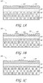
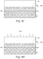
- FIGs. 1A-1C illustrate the cross-section views of a substrate 100 according to some embodiments of the present invention comprising a functionalizable layer 102 comprising one or more functional groups; a polymer layer 103 comprising a plurality of micro-scale or nano-scale patterns, or combinations thereof; and a backing layer 101, where the functionalizable layer 102 is disposed between the backing layer 101 and the polymer layer 103.
- a substrate 100 comprises at least three layers, a backing layer 101, a functionalizable layer 102 and a polymer layer 103.
- the polymer layer 103 comprises a plurality of nano-scale patterns 104 and 105 in different shape and depth. In some other embodiments, the nano-scale patterns of the polymer layer can be the same.
- the polymer layer has a combination of both micro-scale and nano-scale patterns.
- the polymer layer 103 further comprises a plurality of micro-scale patterns 106 and 107, where the nano-scale patterns 104 and 105 are formed within the micro-scale patterns.
- the nano-scale structures can be both nano-wells 104 and nano-posts 108.
- the underlying functionalizable layer 102 is not exposed.
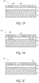
- FIG. 2A illustrate the cross-section view of a substrate 200 according to an embodiment of the present invention having the same layer configuration as those described in FIGs. 1A-1C , where the polymer layer 203 comprises nano-scale patterns 204 and 205. Nano-scale patterns 204 perforate the polymer layer 203 to expose the underlying functionalizable layer 202.
- the functionalizable layer comprises a plurality of micro-scale or nano-scale patterns, or combinations thereof, and at least a portion of the micro-scale or nano-scale patterns of the polymer and functionalizable layers perforate the polymer and functionalizable layers to expose the underlying backing layer.
- FIG. 2B depicts an substrate 200 according to another embodiment of the present invention, where the functionalizable layer 202 comprises a plurality of nano-scale patterns 204 and 206, and nano-scale patterns 206 perforate the polymer layer 203 and the functionalizable layer 202 to expose the underlying backing layer 201.
- each of the nano-scale patterns 204 of the polymer layer 203 perforates the polymer layer to expose the underlying functionalizable layer 202.
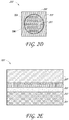
- FIG. 2D illustrates a top view of a substrate of FIG. 2B where nano-scale patterns 204 expose the underlying functionalizable layer 202 and nano-scale patterns 206 perforate the polymer and functionalizable layers to expose the underlying backing layer 201.
- the substrate can further comprise a sealing layer to substantially seal the polymer layer and the functionalizable layer between the backing layer and the sealing layer.
- a sealing layer 207 substantially seals the polymer layer 203 and the functionalizable layer 202 between the sealing layer 207 and the backing layer 201.
- the sealing layer can be optically transparent. In some embodiments, there can be some space in between the sealing layer and the polymer layer to allow sample fluid flowing through.
- the polymer layer is disposed between the backing layer and the functionalizable layer.
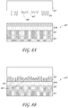
- FIGs. 3A-3C illustrate the cross-section views of a substrate 300 according to some embodiments of the present invention comprising a functionalizable layer 302 comprising one or more functional groups; a polymer layer 303 comprising a plurality of micro-scale or nano-scale patterns, or combinations thereof; and a backing layer 301, where the polymer layer 303 is disposed between the functionalizable layer 302 and the backing layer 301.
- a substrate 300 comprises at least three layers, a backing layer 301, a functionalizable layer 302 and a polymer layer 303, where the polymer layer 303 lays in between the functionalizable layer 302 and the backing layer 301.
- the polymer layer 303 comprises a plurality of nano-scale patterns 304 (nano posts) and 305 (nano wells).
- the nano-scale patterns of the polymer layer can be uniform in size and shape.
- the polymer layer has a combination of both micro-scale and nano-scale patterns.
- the polymer layer 303 further comprises a plurality of micro-scale patterns 306 and 307. In FIGs. 3A and 3B , the underlying polymer layer 303 is not exposed.
- FIG. 3C depicts the cross-section view of the substrate 300 of FIG. 3A when excess functionalizable layer 302 is removed except for those resides within the nano-scale patterns 304 and 305.
- the functionalizable layer comprises a plurality of micro-scale or nano-scale patterns, or combinations thereof, where at least a portion of the micro-scale or nano-scale patterns of the functional layer perforate the functionalizable layer to expose the underlying polymer layer.
- FIG. 4A illustrates the cross-section view of a substrate 400 according to an embodiment of the present invention having a functionalizable layer 402 comprising nano-scale patterns 404 and where the nano-scale patterns 404 perforate the functionalizable layer 402 to expose the underlying polymer layer 403.
- FIG. 4B depicts a substrate 400 according to an embodiment of the present invention, where the functionalizable layer 402 and polymer layer 403 comprise a plurality of nano-scale patterns 406, which perforate the polymer layer 403 and functionalizable layer 402 to expose the underlying backing layer 401, while nano-scale patterns 405 do not perforate the polymer layer 403.
- the polymer layer itself can comprise perforated nano-scale patterns to expose the underlying backing layer 401.
- the substrate can further comprise a sealing layer to substantially seal the polymer layer and the functionalizable layer between the backing layer and the sealing layer.
- a sealing layer 407 substantially seals the polymer layer 403 and the functionalizable layer 402 between the sealing layer 407 and the backing layer 401.
- the sealing layer can be optically transparent. In some embodiments, there can be some space in between the sealing layer and the functionalizable layer to allow sample fluid flowing through.
- the substrate is in the shape of a cylinder.
- the backing layer is closer to an outer surface of the cylinder than the functionalizable or polymer layer of the substrate.
- the backing layer is closer to an inner surface of the cylinder than the functionalizable or polymer layer of the substrate.
- a sample fluid can flow through the inner surface of the cylinder substrate along its longitudinal axis.
- FIGs. 5A, 5B , 6A and 6B are radial cross-section views of substrates 500 and 600 according to some embodiments of the present invention in the shape of a cylinder.
- a backing layer 501 is closer to an outer surface of the cylinder than the functionalizable layer 502 or polymer layer 503 of the substrate 500.
- the functionalizable layer 502 comprises a plurality of nano-scale patterns 504 and 505. Nano-scale patterns 504 perforate the polymer layer 503 to expose the underlying functionalizable layer 502. Nano-scale patterns 505 perforate the polymer layer 503 and the functionalizable layer 502 to expose the underlying backing layer 501.
- the backing layer 501 is closer to an inner surface of the cylinder than the functionalizable layer 502 or polymer layer 503 of the substrate 500.
- FIG. 6A illustrate a substrate 600 according to an embodiment of the present application with a backing layer 601 is closer to an outer surface of the cylinder than the functionalizable layer 602 or polymer layer 603 of the substrate 600.
- the functionalizable layer 602 comprises a plurality of nano-scale patterns 604 and 605. Nano-scale patterns 604 perforate the functionalizable layer 602 to expose the underlying polymer layer 603 and nano-scale patterns 605 perforate the polymer layer 603 and functionalizable layer 602 to expose the underlying backing layer 601.
- the backing layer 601 of the substrate 600 according to an embodiment of the present application is closer to an inner surface of the cylinder than the functionalizable layer 602 or polymer layer 603 of the substrate 600.
- FIGs. 7A and 7B are cross-section views of a substrate 700 according to some embodiments of the present application formed by two substrates, where the polymer layers 703 and the functionalizable layers 702 are substantially sealed in between two backing layers 701.
- the substrate 700 is formed by stacking substrate 700a on the distal surface of the substrate 700b such that the distal surface of the two polymer layers 703 are in contact with each other (the distal surface being referenced to the backing layer).
- Both substrates 700a and 700b comprise nano-scale patterns 704 and 705 in the polymer layers 703, where nano-scale patterns 705 perforate the polymer layers 703 to expose the underlying functionalizable layers 702.
- the substrate 700 is formed by stacking one substrate 700a on the distal surface of another substrate 700a such that the distal surfaces of the two functionalizable layers 702 are within close proximity to each other (e.g. in many embodiments the distal surfaces are in direct contact with each other).
- Nano-scale patterns 706 perforate the polymer layers 703 and the functionalizable layers 702 to expose the underlying backing layers 701. The spacing between the two functionalizable layers 702 can allow a sample fluid flowing through.
- One or more edges of the substrate 700 can be substantially sealed to avoid fluid leaking.
- the substrate can further comprise a sealing layer to substantially seal the polymer layer and the functionalizable layer between the backing layer and the sealing layer.
- the sealing layer is optically transparent.
- At least one of the micro-scale or nano-scale patterns is capable of admitting a sample fluid.
- the substrate can further comprise a fluid reservoir, for example, a sample, reagent or waste reservoir.
- the micro-scale or nano-scale patterns of the polymer layer can comprise channels, trenches, wells, posts, or combinations thereof.
- at least a portion of the micro-scale or nano-scale patterns are posts.
- the posts have an average diameter of less than about 500 nm.
- the posts have an average diameter of about 330 nm or less including, for example, less than about 300 nm, 200 nm, 100 nm, or 50 nm.
- the posts have an average height of less than about 500 nm.
- the posts have an average height of about 300 nm or less including, for example, less than about 300 nm, 200 nm, 100 nm, or 50 nm.
- the average diameter and/or average height of the posts can be at most 1 mm, 500 ⁇ m, 100 ⁇ m, 1 ⁇ m, 500 nm, 400 nm, 300 nm, 200 nm or 100 nm.
- the plurality of micro-scale or nano-scale patterns, or combinations thereof, are made by mechanical embossing at room temperature.
- the functionalizable layer can comprise a reactive silane layer, functionalizable hydrogel or a functionalizable polymer.
- the functionalizable layer can comprise one or more functional groups.
- the functional group can be selected from the group consisting of optionally substituted alkene, azide, optionally substituted amine, carboxylic acid, optionally substituted hydrazone, halogen, hydroxy, optionally substituted tetrazole, optionally substituted tetrazine, thiol, and combinations thereof.
- the functionalizable layer comprises a polymer or hydrogel comprising Formula (Ia) or (Ib):
- R 1 is H or optionally substituted alkyl
- the functional group R A is selected from the group consisting of azide, optionally substituted amine, optionally substituted alkene, optionally substituted hydrazone, carboxylic acid, halogen, hydroxy, optionally substituted tetrazole, optionally substituted tetrazine, and thiol
- R 5 is selected from H or optionally substituted alkyl
- each of the -(CH 2 )-p can be optionally substituted
- p is an integer in the range of 1 to 50
- n is an integer in the range of 1 to 50,000
- m is an integer in the range of 1 to 100,000.
- the functional groups comprise azides.
- each R 1 and R 5 is hydrogen.
- the functional group R A is azide.
- p is 5.
- the polymer or hydrogel comprised in the functionalizable layer is PAZAM. Methods for making and using PAZAM, and other functionalizable materials that can be used in a layer of a substrate of the present disclosure are described in U.S. Pat. App. Ser. Nos. 13/784,368 and 61/841,647 .
- reactive silanes examples include, but are not limited to, acrylate functional silanes, aldehyde functional silanes, amino functional silanes, anhydride functional silanes, azide functional silanes, carboxylate functional silanes, phosphonate functional silanes, sulfonate functional silanes, epoxy functional silanes, ester functional silanes, vinyl functional silanes, olefin functional silanes, halogen functional silanes and dipodal silanes with any or none of the above functional groups.
- Norbornene silanes are particularly useful and are described, for example, in U.S. Pat. App. Ser. No. 61/841,647 .
- silane functionality can be made based on the reactivity of the material to which it will react.
- amino functional silanes react with thermoplastics such as polyacrylate, polyamide, polyamide-imide, polybutylene terephthalate, polycarbonate, polyether ketone, polyethylene, polyphenylene sulfide, polysulfone, polyvinyl butyral and polyvinyl chloride.
- Vinyl and olefin functional silanes react with thermoplastics such as polyacetal, polyethylene, and polypropylene.
- Acrylate functional silanes react with thermoplastics such as polypropylene, and polystyrene.
- the functional groups of the functionalizable layer are attached to biomolecules.
- the biomolecules are selected from amino acids, nucleosides, nucleotides, peptides, oligonucleotides, polynucleotides, nucleic acids, proteins, or combinations thereof. In some such embodiments, the biomolecules are nucleic acids.
- the functionalizable layer can comprise a hydrogel.
- hydrogels can be used in the present application are described herein.
- WO 00/31148 discloses polyacrylamide hydrogels and polyacrylamide hydrogel-based arrays in which a so-called polyacrylamide prepolymer is formed, preferably from acrylamide and an acrylic acid or an acrylic acid derivative containing a vinyl group. Crosslinking of the prepolymer may then be affected.
- the hydrogels so produced are solid-supported, preferably on glass. Functionalization of the solid-supported hydrogel may also be effected.
- WO 01/01143 describes technology similar to WO00/31148 but differing in that the hydrogel bears functionality capable of participating in a [2+2] photocycloaddition reaction with a biomolecule so as to form immobilized arrays of such biomolecules.
- Dimethylmaleimide (DMI) is a particularly preferred functionality.
- the use of [2+2] photocycloaddition reactions, in the context of polyacrylamide-based microarray technology is also described in WO02/12566 and WO03/014392 .
- U.S. Pat. No. 6,465,178 discloses the use of reagent compositions in providing activated slides for use in preparing microarrays of nucleic acids; the reagent compositions include acrylamide copolymers.
- WO 00/53812 discloses the preparation of polyacrylamide-based hydrogel arrays of DNA and the use of these arrays in replica amplification.
- hydrogels Once hydrogels have been formed, biomolecules may then be attached to them so as to produce molecular arrays, if desired. Attachment has been effected in different ways.
- U.S. Pat. No. 6,372,813 teaches immobilization of polynucleotides bearing dimethylmaleimide groups to the hydrogels produced which bear dimethylmaleimide groups by conducting a [2+2] photocycloaddition step between two dimethylmaleimide groups-one attached to the polynucleotide to be immobilized and one pendant from the hydrogel.
- the hydrogel may be modified chemically after it is produced.
- a more common alternative is to effect polymerization with a co-monomer having a functionality primed or pre-activated to react with the molecules to be arrayed.
- ACRYDITETM an acrylamide phosphoramidite
- compositions and methods set forth above and in the references cited above can be used in the compositions and methods set forth herein.
- the hydrogels can be used as functionalizable layers in a substrate set forth herein.
- the functionalizable layer can comprise a polymer with one or more functional groups that are capable of reacting with biomolecules of interest.
- the functional group can be selected from the group consisting of optionally substituted alkene, azide, optionally substituted amine, carboxylic acid, optionally substituted hydrazone, halogen, hydroxy, optionally substituted tetrazole, optionally substituted tetrazine, thiol, and combinations thereof.
- Non-limiting examples of the polymers can be used in the present application are described herein, including those described in U.S. Ser. No. 13/784,368 and U.S. Pat. Pub. No. 2011/0059865 , which are hereby incorporated by references in their entireties.
- the polymer of Formula (Ia) or (Ib) is also represented by Formula (IIa) or (IIb): wherein n is an integer in the range of 1-20,000, and m is an integer in the range of 1-100,000.
- the functionalized molecule used for direct conjugation is poly(N-(5-azidoacetamidylpentyl)acrylamide-co-acrylamide) (PAZAM).
- PAZAM can be prepared by polymerization of acrylamide and Azapa (N-(5-(2-azidoacetamido)pentyl)acrylamide) in any ratio.
- PAZAM is a linear polymer.
- PAZAM is a lightly cross-linked polymer.
- PAZAM is applied as an aqueous solution.
- PAZAM is applied as an aqueous solution with one or more solvent additives, such as ethanol.
- solvent additives such as ethanol
- the polymer layer can comprise at least one photocurable polymer.
- the photocurable polymer comprises a urethane, acrylate, silicone, epoxy, polyacrylic acid, polyacrylates, epoxysilicone, epoxy resins, polydimethylsiloxane (PDMS), silsesquioxane, acyloxysilanes, maleate polyesters, vinyl ethers, monomers with vinyl or ethynyl groups, or copolymers and combinations thereof.
- the backing layer may be, for example, no more than about 10 nm, 50 nm, 100 nm, 1 ⁇ m, 10 ⁇ m, 100 ⁇ m, 500 ⁇ m, 1 mm, 5 mm, 1 cm, or 10 cm in thickness.
- the backing layer is no less than about 10 nm, 50 nm, 100 nm, 1 ⁇ m, 10 ⁇ m, 100 ⁇ m, 500 ⁇ m, 1 mm, 5 mm, 1 cm, or 10 cm in thickness.
- the polymer layer is no more than about the length of a carbon-carbon bond, 1 nm, 10 nm, 50 nm, 100 nm, 1 ⁇ m, 10 ⁇ m, 100 ⁇ m, 500 ⁇ m, 1 mm, 5 mm, 1 cm, or 10 cm in thickness. In some embodiments, the polymer layer is no less than about 10 nm, 50 nm, 100 nm, 1 ⁇ m, 10 ⁇ m, 100 ⁇ m, 500 ⁇ m, 1 mm, 5 mm, 1 cm, or 10 cm in thickness.
- the functionalizable layer is no more than about the length of a carbon-carbon bond, 1 nm, 10 nm, 50 nm, 100 nm, 1 ⁇ m, 10 ⁇ m, 100 ⁇ m, 500 ⁇ m, 1 mm, 5 mm, 1 cm, or 10 cm in thickness. In some embodiments, the functionalizable layer is no less than about 10 nm, 50 nm, 100 nm, 1 ⁇ m, 10 ⁇ m, 100 ⁇ m, 500 ⁇ m, 1 mm, 5 mm, 1 cm, or 10 cm in thickness.
- Exemplary dicing tapes that can be used in a composition or method set forth herein include, but are not limited to, Lintec KL-3225 UV tape; Ultron Systems, Anti-Static UV Adhesive Plastic Film (p/n: 1043R-9.05), or AIT UVR250 (AI Technology Inc., Princeton Junction, NJ). Other useful dicing tapes are commercially available from Semiconductor Equipment Corp.
- the backing layer can be made of a material selected from the group consisting of silica, plastic, quartz, metal, metal oxide, paper and combinations thereof.
- the backing layer is made of a flexible plastic material.
- the flexible plastic material has a stiffness that is sufficient to preclude the backing layer from conforming to nano-scale or micro-scale contours on a solid support when the backing layer is contacted with the solid support in a method set forth herein.
- the contacting between the solid support and backing layer may occur under sufficient pressure that a negative replicate of the nano-scale or micro-scale contours is transferred to an adhesive layer that is attached to the backing layer; yet the backing layer will have sufficient stiffness to resist deformation permanently or in some cases even temporarily.
- the backing layer is made from a roll of thin flexible film. Non-limiting examples of backing layers that can be used in the present application are described herein.
- backing layers used in the present application include silica-based materials, such as glass, fused silica and other silica-containing materials.
- silica-based substrates can also be silicon, silicon dioxide, silicon nitride, silicone hydrides.
- backing layers used in the present application include plastic materials such as polyethylene, polystyrene, poly(vinyl chloride), polypropylene, nylons, polyesters, polycarbonates and poly(methyl methacrylate). Preferred plastics materials are poly(methyl methacrylate), polystyrene and cyclic olefin polymer substrates.
- the backing layer can be a metal.
- the metal is gold.
- the backing layer has at least one surface comprising a metal oxide. In one embodiment, the surface comprises a tantalum oxide.
- Acrylamide, enone, or acrylate may also be utilized as a backing layer material.
- Other backing layer materials can include, but are not limited to gallium aresnide, indium phosphide, aluminum, ceramics, polyimide, quartz, resins, polymers and copolymers. The foregoing lists are intended to be illustrative of, but not limited to the present application.
- the backing layer and/or the backing layer surface can be quartz. In some other embodiments, the backing layer and/or the backing layer surface can be semiconductor, i.e. GaAs or ITO.
- the backing layer is made of paper.
- the backing layer is made of a flexible material.
- the backing layer is made from a roll of thin flexible film (for example, having a thickness of less than about 1 mm, 500 ⁇ m, 100 ⁇ m, or less.
- Backing layers can comprise a single material or a plurality of different materials, for example, two or more layers of one or more materials.
- the shape of the backing layers employed may be varied in accordance with the application for which the present application is practiced.
- One or more of the layers that is present in a composition or used in a method set forth herein can be doped with a material having a desired characteristic.
- a layer can have plasmonic properties due to the presence of nanoparticles, Q dots or the like spiked into the material of the layer.
- the resulting plasmonic properties can provide an antenna effect during a subsequent detection step that is carried out in or on the doped layer.
- a layer can be doped with receptors, ligands or nucleic acids to provide binding specificity in an analytical detection application; or doped with reactive moieties, such as those set forth herein in the context of functionalizable layers, to provide for subsequent functionalization; or doped with materials that alter optical properties of the layer such as optical filter materials, materials that absorb light in a particular wavelength range, materials that emit light in a particular wavelength range, or materials that scatter light; or doped with materials that impart conductive characteristics such as electrical conductivity; or doped with materials that are thermally conductive.
- a layer can be doped prior to use in a method set forth herein.
- one or more layer of a substrate can be doped prior to creation of a pattern in the substrate.
- a polymer layer or functionalizable layer can be doped prior to creation of a pattern in the polymer layer.
- the dopant material in the polymer layer will form part of the pattern, being displaced from some regions of the pattern and retained in other regions of the pattern.
- a dopant material that is in a functionalizable layer can be exposed in some portions of the pattern and protected in other parts of the pattern to allow for selective detection or reactivity of the exposed portions in a subsequent use of the substrate.
- One or more of the layers set forth herein can be doped, including, for example, a polymer layer, functionalizable layer, or backing layer.
- the dopant material can be present primarily or solely on the surface of a layer, within the volume of a layer, or both within the layer and on the surface of the layer.
- a substrate described herein forms at least part of a flow cell or is located in a flow cell.
- the flow cells further comprise polynucleotides attached to the surface of the substrate via reaction with the functional groups of the functionalizable layer, for example, a hydrogel coating.
- the functionalizable layer is disposed between the polymer layer and the backing layer, with at least a portion of the micro-scale or nano-scale patterns of the polymer layer are perforated to expose the underlying functionalizable layer.
- the polymer layer is disposed between the functionalizable layer and the backing layer, with at least a portion of the micro-scale or nano-scale patterns of the functionalizable layer are perforated to expose the underlying polymer layer.
- the polynucleotides are present in the flow cells in polynucleotide clusters, wherein the polynucleotides of the polynucleotide clusters are attached to a surface of the flow cell via the hydrogel coating.
- Clusters can be formed by solid-phase amplification techniques such as solid-phase PCR, bridge amplification or other techniques known in the art or described in U.S. Pat. No. 5,641,658 ; U.S. Patent Publ. No. 2002/0055100 ; U.S. Pat. No. 7,115,400 ; U.S. Patent Publ. No. 2004/0096853 ; U.S. Patent Publ. No. 2004/0002090 ; U.S. Patent Publ.
- the flow cell is a flow chamber that is divided into a plurality of lanes or a plurality of sectors, wherein one or more of the plurality of lanes or plurality of sectors comprises a surface that is coated with a covalently attached functionalizable hydrogel coating described herein.
- the attached polynucleotides within a single polynucleotide cluster have the same or similar nucleotide sequence.
- the attached polynucleotides of different polynucleotide clusters have different or nonsimilar nucleotide sequences.
- Exemplary flow cells and substrates for manufacture of flow cells that can be used in method or composition set forth herein include, but are not limited to, those commercially available from Illumina, Inc. (San Diego, CA) or described in US 2010/0111768 A1 or US 2012/0270305 , each of which is incorporated herein by reference.
- a substrate described herein forms at least part of a microfluidic device or is located within a microfluidic device.
- Exemplary devices include flow cells useful in nucleic acid sequencing and other analytical procedures such as the flow cells commercially available from Illumina, Inc. (San Diego, CA) or described in U.S. 2010/0111768 A1 or U.S. 2012/0270305 A1 , each of which is incorporated herein by reference.
- Other microfluidic devices include cell sorting devices, lab on a chip devices, capillary sequencers, cell counting devices and the like can also be prepared at least in part from a substrate described herein or comprise a substrate described herein.
- Some embodiments disclosed herein include a process for preparing a substrate, comprising: providing a substrate comprising a functionalizable layer comprising one or more functional groups disposed between a backing layer and a layer of photocurable polymer; contacting a surface of the layer of photocurable polymer with a template having a plurality of micro-scale or nano-scale patterns including micro-scale or nano-scale wells, posts, channels, junctions or combinations thereof; applying pressure to the template or substrate to transfer the micro-scale or nano-scale patterns to at least the layer of photocurable polymer, where the contacting and applying are performed at room temperature; irradiating the photocurable polymer with UV light to cure the photocurable polymer; and separating the template from substrate; where at least a portion of the polymer layer is perforated to expose the underlying functionalizable layer.
- FIGs. 8A - 8D are cross-section views to illustrate a UV nano-embossing process to prepare a substrate 800 according to an embodiment of the present invention.
- an embossed stamp 804 comprises a plurality of nano-scale patterns 805 and 806 thereon, and a plurality of grooves 807 in between the nano-scale patterns.
- a substrate 800 comprising a backing layer 801, a functionalizable layer 802 and a photocurable polymer layer 803a is also provided.
- the embossed stamp 804 is contacted with an upper surface of the photocurable polymer layer 803a, then pressure is applied to the embossed stamp 804 or the substrate 800 as shown in FIG. 8B .
- the nano-scale patterns 805 and 806 are formed in the photocurable polymer layer 803a of the substrate 800.
- UV light is irradiated onto the UV curable polymer layer 803a through the embossed stamp 804 as shown in FIG. 8C .
- the embossed stamp 804 is made of a material that allows UV light to pass through such that UV light reaches the photocurable polymer layer 803a and cure the photocurable polymer, forming a polymer layer 803.
- the UV light can be applied through the backing layer 801 if the backing layer and functionalizable layer 802 are made of materials that allow UV light to pass through.
- Nano-scale patterns 805 perforate the polymer layer 803 to expose the underlying functionalizable layer 802.
- Some embodiments disclosed herein include a process for preparing a substrate, comprising: providing a template comprising a plurality of micro-scale or nano-scale patterns including micro-scale or nano-scale wells, channels or combinations thereof on a surface of the template; depositing a functional layer comprising one or more functional groups on the surface of the template such that at least a portion of the micro-scale or nano-scale wells, channels or combinations thereof contain the functional layer; removing excess functionalizable layer from the surface of the template such that the functionalizable layer is present on only a portion of the template surface; providing a substrate comprising a backing layer having a photocurable polymer layer disposed on the backing layer; contacting a surface of the photocurable polymer layer with the surface of the template having the plurality of micro-scale or nano-scale patterns and functionalizable layer thereon; applying pressure to the template or substrate to transfer the micro-scale or nano-scale pattern to at least the layer of photocurable polymer, where the contacting and applying are performed at room temperature; i
- FIGs. 9A - 9E are cross-section views to illustrate a UV nano-embossing process to prepare a substrate 900 according to an embodiment of the present invention.
- an embossed stamp 904 comprises a plurality of nano-scale patterns 905 thereon, and a plurality of grooves 906 in between the nano-scale patterns 905.
- a functionalizable layer 902 is deposited on the nano-scale patterned surface of the embossed stamp 904.
- excess functionalizable layer 902 is removed such that the functionalizable layer is only present within the nano-scale patterns 905 of the embossed stamp 904.
- a substrate 900a having a backing layer 901 and a photocurable polymer layer 903a is provided.
- the embossed stamp 904 is contacted with an upper surface of the photocurable polymer layer 903a, and then pressure is applied to the embossed stamp 904 or the substrate 900a as shown in FIG. 9C .
- the nano-scale patterns 905 are formed in the photocurable polymer layer 903a of the substrate 900a.
- UV light is irradiated onto the UV curable polymer layer 903a through the embossed stamp 904 as shown in FIG. 9D .
- the embossed stamp 904 is made of a material that allows UV light to pass through such that UV light reaches the photocurable polymer layer 903a and cure the photocurable polymer, forming a polymer layer 903.
- the UV light can be applied through the backing layer 901 if the backing layer 901 is made of materials that allow UV light to pass through.
- the embossed stamp 904 is separated from the polymer layer 903.
- the functionalizable layer 902 is transferred to the top surface of the polymer layer 903.
- nano-scale patterns 905 are formed in the polymer layer 903 as shown in FIG. 9E .
- the embossed stamp can have micro-scale or nano-scale patterns that result in at least a portion of polymer layer and functionalizable layer being perforated to expose the underlying backing layer.
- the substrate further comprises a backing layer having a photocurable polymer layer disposed on the backing layer is a roll of flexible dicing tape.
- the process can further comprises applying a sealing layer to the substrate after removing the template to substantially seal the polymer layer and the functionalizable layer between the backing layer and the sealing layer.
- the sealing layer further comprises a second substrate prepared by the process of any of the disclosed embodiments, where the functionalizable layers and photocurable polymer layers of the substrates are disposed between the backing layers of the substrates.
- the sealing layer is optically transparent.
- the process can further comprise forming the substrate into a cylinder.
- the backing layer is closer to an outer surface of the cylinder than the functionalizable or polymer layer of the substrate.
- the backing layer is closer to an inner surface of the cylinder than the functionalizable or polymer layer of the substrate.
- the cylindrical shaped substrate can be formed using a flexible backing layer and wrapping the substrate around a cylindrical object, such as a glass or plastic rod or capillary.
- the process can be a roll to roll process.
- An 8" master template wafer containing 12 Hi-seq sized patterned flowcells was used to emboss directly into a UV curable adhesive coated polymer sheet ( FIG. 10A ).
- the template wafer with nano-scale patterned structures was aligned with a polymer sheet coated with a UV curable adhesive layer such that the adhesive layer was in direct contact with the nano patterned surface.
- Mechanical force was applied on the polymer sheet's non-adhesive surface.
- the polymer sheet was irradiated with UV light to cure the adhesive and the polymer sheet was released by delamination.
- high fidelity pattern transfer from the template to the polymer sheet was observed.
- Diffraction patterns from flowcell regions confirm large area pattern transfer.
- Flowcell 7 was cut out of the polymer sheet for further microscope inspection and electron microscopy.
- FIG. 10B dark field microscope image of a fiducial from FC7 confirms nano-scale patterns transfer.
- the master template in this case contained 350 nm nano-well features with 750 nm pitch.
- the pattern transferred into the polymer sheet was the opposite polarity as the pattern in the template (nano-posts).
- SEM images of fiducial region of the FC7 at 1240X and 20kX magnifications are illustrated in FIGs. 10C and 10D .
- nano-scale pillars on polymer sheet at 40 kX and 80 kX magnifications are illustrated in FIGs. 10E and 10F .
- Excellent pattern transfer was seen in all cases with post diameters in the range of about 330 nm and a post-height of about 300 nm.
- the polarity of nano-scale patterns of the master template was reversed as compared to the master template described in Example 1.
- the master template comprises nano-scale posts instead of nano-well features.
- the same pattern transfer process as described in Example 1 was used to generate the opposite polarity pattern on the polymer sheet.
- the formation of nano-wells and nano-trenches in the polymer sheet following physical embossing and UV curing are shown in FIGs. 11A and 11B with different magnification. High fidelity, high throughput pattern transfer was achieved.
- a silicon master template comprising microfluidic structures in patterned SU-8 photoresist was prepared. Then the silicon master wafer was imprinted into a clear polymer sheet with a UV curable adhesive layer such that the microfluidic pattern was in direct contact with the adhesive layer. After standard UV radiation and release process as described in Example 1, multiple 4-inch polymer replicas of the master wafer were formed in less than 2 minutes. The patterned microfluidic structures transferred are shown in FIGs. 12A-12D . These fluidic structures were formed in commercially available dicing tape (Lintec KL-3225 UV tape or Ultron Systems, Anti-Static UV Adhesive Plastic Filmp/n: 1043R-9.05).
- FIG. 12A depicts serpentine fluidic channels and junctions formed for applications such as fluidic mixing.
- Microfluidic filters FIG. 12B
- FIG. 12D shows an optical image of the fluid flowed into a T-junction for fluid mixing.
Applications Claiming Priority (3)
| Application Number | Priority Date | Filing Date | Title |
|---|---|---|---|
| US201361918582P | 2013-12-19 | 2013-12-19 | |
| PCT/US2014/070777 WO2015095291A1 (en) | 2013-12-19 | 2014-12-17 | Substrates comprising nano-patterning surfaces and methods of preparing thereof |
| EP14824694.5A EP3084523B1 (de) | 2013-12-19 | 2014-12-17 | Substrate mit nanostrukturierungsoberflächen und verfahren zur herstellung davon |
Related Parent Applications (1)
| Application Number | Title | Priority Date | Filing Date |
|---|---|---|---|
| EP14824694.5A Division EP3084523B1 (de) | 2013-12-19 | 2014-12-17 | Substrate mit nanostrukturierungsoberflächen und verfahren zur herstellung davon |
Publications (1)
| Publication Number | Publication Date |
|---|---|
| EP3572875A1 true EP3572875A1 (de) | 2019-11-27 |
Family
ID=52293256
Family Applications (2)
| Application Number | Title | Priority Date | Filing Date |
|---|---|---|---|
| EP14824694.5A Active EP3084523B1 (de) | 2013-12-19 | 2014-12-17 | Substrate mit nanostrukturierungsoberflächen und verfahren zur herstellung davon |
| EP19183860.6A Pending EP3572875A1 (de) | 2013-12-19 | 2014-12-17 | Roll-to-roll-verfahren zur herstellung eines strukturierten substrats und mittels diesem verfahren hergestelltes strukturiertes substrat |
Family Applications Before (1)
| Application Number | Title | Priority Date | Filing Date |
|---|---|---|---|
| EP14824694.5A Active EP3084523B1 (de) | 2013-12-19 | 2014-12-17 | Substrate mit nanostrukturierungsoberflächen und verfahren zur herstellung davon |
Country Status (7)
| Country | Link |
|---|---|
| US (3) | US10682829B2 (de) |
| EP (2) | EP3084523B1 (de) |
| JP (3) | JP6683608B2 (de) |
| CN (2) | CN114089597A (de) |
| AU (1) | AU2014364898B2 (de) |
| CA (2) | CA2928598C (de) |
| WO (1) | WO2015095291A1 (de) |
Families Citing this family (32)
| Publication number | Priority date | Publication date | Assignee | Title |
|---|---|---|---|---|
| KR102590448B1 (ko) * | 2014-11-11 | 2023-10-17 | 일루미나 케임브리지 리미티드 | 핵산의 모노클로날 클러스터를 형성시키고 시퀀싱하기 위한 방법 및 어레이 |
| CN107924121B (zh) | 2015-07-07 | 2021-06-08 | 亿明达股份有限公司 | 经由纳米压印的选择性表面图案化 |
| ES2945607T3 (es) * | 2015-07-17 | 2023-07-04 | Illumina Inc | Láminas de polímero para aplicaciones de secuenciación |
| US20190030530A1 (en) * | 2016-02-02 | 2019-01-31 | Okinawa Institute Of Science And Technology School Corporation | Micro- and nanocontact printing with aminosilanes: patterning surfaces of microfluidic devices for multi- plexed bioassays |
| CN109313396B (zh) | 2016-05-18 | 2022-11-22 | Illumina公司 | 使用图案化疏水性表面进行的自组装图案化 |
| DE102016109693B4 (de) * | 2016-05-25 | 2022-10-27 | Infineon Technologies Ag | Verfahren zum Trennen von Halbleiterdies von einem Halbleitersubstrat und Halbleitersubstratanordnung |
| CN109844638B (zh) * | 2016-09-27 | 2024-03-15 | 伊鲁米那股份有限公司 | 压印基板 |
| CN106501520A (zh) * | 2016-10-18 | 2017-03-15 | 成都市亿泰科技有限公司 | 一种基于微流体毛细结构的毒品检测试纸及其制备方法 |
| BR112019013079A2 (pt) | 2016-12-22 | 2020-06-16 | Illumina, Inc. | Matriz incluindo iniciador de sequenciamento e entidade de não sequenciamento |
| CN110248725B (zh) * | 2016-12-22 | 2022-08-02 | 伊鲁米那股份有限公司 | 包括树脂膜和图案化的聚合物层的阵列 |
| MY196044A (en) | 2016-12-22 | 2023-03-09 | Illumina Inc | Flow Cell Package And Method For Making The Same |
| JP7084402B2 (ja) * | 2016-12-22 | 2022-06-14 | イラミーナ インコーポレーテッド | インプリント装置 |
| US11261085B2 (en) | 2017-05-03 | 2022-03-01 | Nanotech Security Corp. | Methods for micro and nano fabrication by selective template removal |
| WO2018201248A1 (en) * | 2017-05-03 | 2018-11-08 | Nanotech Security Corp. | Methods for micro and nano fabrication by selective template removal |
| US10503456B2 (en) | 2017-05-05 | 2019-12-10 | Nvidia Corporation | Method and apparatus for rendering perspective-correct images for a tilted multi-display environment |
| CN110741463B (zh) * | 2017-06-09 | 2024-02-20 | 三井化学株式会社 | 带有微细凹凸图案的基板的制造方法、树脂组合物及层叠体 |
| DE102017217179A1 (de) * | 2017-09-27 | 2019-03-28 | Disco Corporation | Mikrofluidisches System oder mikrofluidische Einrichtung und Verfahren zum Herstellen eines mikrofluidischen Systems oder einer mikrofluidischen Einrichtung |
| KR102091622B1 (ko) * | 2017-10-10 | 2020-03-20 | 삼육대학교산학협력단 | 양자점-중합체 합성물의 패턴화 방법 및 패턴화된 양자점-중합체 합성물을 포함하는 기판 |
| US10344328B2 (en) | 2017-11-17 | 2019-07-09 | Ultima Genomics, Inc. | Methods for biological sample processing and analysis |
| US11499962B2 (en) | 2017-11-17 | 2022-11-15 | Ultima Genomics, Inc. | Methods and systems for analyte detection and analysis |
| CN111093819B (zh) * | 2017-12-21 | 2022-04-05 | 伊鲁米纳公司 | 具有水凝胶涂层的流动池 |
| SG11201911980WA (en) * | 2017-12-22 | 2020-01-30 | Illumina Inc | Catalytically active substances |
| US10512911B1 (en) | 2018-12-07 | 2019-12-24 | Ultima Genomics, Inc. | Implementing barriers for controlled environments during sample processing and detection |
| WO2020141056A1 (en) * | 2018-12-31 | 2020-07-09 | Asml Netherlands B.V. | Method for predicting resist deformation |
| US10900078B2 (en) | 2019-03-14 | 2021-01-26 | Ultima Genomics, Inc. | Methods, devices, and systems for analyte detection and analysis |
| US11118223B2 (en) | 2019-03-14 | 2021-09-14 | Ultima Genomics, Inc. | Methods, devices, and systems for analyte detection and analysis |
| US10852518B1 (en) | 2019-03-14 | 2020-12-01 | Ultima Genomics, Inc. | Methods, devices, and systems for analyte detection and analysis |
| US10830703B1 (en) | 2019-03-14 | 2020-11-10 | Ultima Genomics, Inc. | Methods, devices, and systems for analyte detection and analysis |
| NL2023679B1 (en) * | 2019-08-09 | 2021-04-13 | Illumina Inc | System and method for patterning flow cell substrates |
| CN110596950A (zh) | 2019-10-29 | 2019-12-20 | 京东方科技集团股份有限公司 | 一种量子点彩色滤光层及其制作方法、显示面板及装置 |
| EP3839625A1 (de) * | 2019-12-18 | 2021-06-23 | Nivarox-FAR S.A. | Verfahren zur herstellung einer uhrkomponente und nach diesem verfahren hergestellte komponente |
| US20240033738A1 (en) * | 2022-07-27 | 2024-02-01 | Illumina, Inc. | Flow cell based motion system calibration and control methods |
Citations (53)
| Publication number | Priority date | Publication date | Assignee | Title |
|---|---|---|---|---|
| WO1993017126A1 (en) | 1992-02-19 | 1993-09-02 | The Public Health Research Institute Of The City Of New York, Inc. | Novel oligonucleotide arrays and their use for sorting, isolating, sequencing, and manipulating nucleic acids |
| WO1995011995A1 (en) | 1993-10-26 | 1995-05-04 | Affymax Technologies N.V. | Arrays of nucleic acid probes on biological chips |
| US5429807A (en) | 1993-10-28 | 1995-07-04 | Beckman Instruments, Inc. | Method and apparatus for creating biopolymer arrays on a solid support surface |
| US5436327A (en) | 1988-09-21 | 1995-07-25 | Isis Innovation Limited | Support-bound oligonucleotides |
| WO1995035505A1 (en) | 1994-06-17 | 1995-12-28 | The Board Of Trustees Of The Leland Stanford Junior University | Method and apparatus for fabricating microarrays of biological samples |
| US5561071A (en) | 1989-07-24 | 1996-10-01 | Hollenberg; Cornelis P. | DNA and DNA technology for the construction of networks to be used in chip construction and chip production (DNA-chips) |
| EP0742287A2 (de) | 1995-05-10 | 1996-11-13 | McGall, Glenn H. | Modifizierte Nukleinsäuresonden |
| US5583211A (en) | 1992-10-29 | 1996-12-10 | Beckman Instruments, Inc. | Surface activated organic polymers useful for location - specific attachment of nucleic acids, peptides, proteins and oligosaccharides |
| US5641658A (en) | 1994-08-03 | 1997-06-24 | Mosaic Technologies, Inc. | Method for performing amplification of nucleic acid with two primers bound to a single solid support |
| US5658734A (en) | 1995-10-17 | 1997-08-19 | International Business Machines Corporation | Process for synthesizing chemical compounds |
| EP0799897A1 (de) | 1996-04-04 | 1997-10-08 | Affymetrix, Inc. (a California Corporation) | Verfahren und Zusammensetzungen zur Selektion von Tag-Nukleinsäuren und entsprechende Proben |
| US5837858A (en) | 1993-10-22 | 1998-11-17 | The Board Of Trustees Of The Leland Stanford Junior University | Method for polymer synthesis using arrays |
| US5874219A (en) | 1995-06-07 | 1999-02-23 | Affymetrix, Inc. | Methods for concurrently processing multiple biological chip assays |
| US5919523A (en) | 1995-04-27 | 1999-07-06 | Affymetrix, Inc. | Derivatization of solid supports and methods for oligomer synthesis |
| WO2000031148A2 (en) | 1998-11-25 | 2000-06-02 | Motorola, Inc. | Polyacrylamide hydrogels and hydrogel arrays made from polyacrylamide reactive prepolymers |
| WO2000053812A2 (en) | 1999-03-12 | 2000-09-14 | President And Fellows Of Harvard College | Replica amplification of nucleic acid arrays |
| US6136269A (en) | 1991-11-22 | 2000-10-24 | Affymetrix, Inc. | Combinatorial kit for polymer synthesis |
| WO2000063437A2 (en) | 1999-04-20 | 2000-10-26 | Illumina, Inc. | Detection of nucleic acid reactions on bead arrays |
| WO2001001143A2 (en) | 1999-06-25 | 2001-01-04 | Motorola Inc. | Attachment of biomolecule to a polymeric solid support by cycloaddition of a linker |
| WO2001062982A2 (en) | 2000-02-25 | 2001-08-30 | Mosaic Technologies, Inc. | Methods for multi-stage solid phase amplification of nucleic acids |
| US6288220B1 (en) | 1998-03-05 | 2001-09-11 | Hitachi, Ltd. | DNA probe array |
| US6287776B1 (en) | 1998-02-02 | 2001-09-11 | Signature Bioscience, Inc. | Method for detecting and classifying nucleic acid hybridization |
| US6287768B1 (en) | 1998-01-07 | 2001-09-11 | Clontech Laboratories, Inc. | Polymeric arrays and methods for their use in binding assays |
| US6291193B1 (en) | 1998-06-16 | 2001-09-18 | Millennium Pharmaceuticals, Inc. | MTbx protein and nucleic acid molecules and uses therefor |
| US6297006B1 (en) | 1997-01-16 | 2001-10-02 | Hyseq, Inc. | Methods for sequencing repetitive sequences and for determining the order of sequence subfragments |
| US6346413B1 (en) | 1989-06-07 | 2002-02-12 | Affymetrix, Inc. | Polymer arrays |
| WO2002012566A2 (en) | 2000-08-09 | 2002-02-14 | Motorola, Inc. | The use and evaluation of a [2+2] photocycloaddition in immobilization of oligonucleotides on a three-dimensional hydrogel matrix |
| US6355431B1 (en) | 1999-04-20 | 2002-03-12 | Illumina, Inc. | Detection of nucleic acid amplification reactions using bead arrays |
| US20020055100A1 (en) | 1997-04-01 | 2002-05-09 | Kawashima Eric H. | Method of nucleic acid sequencing |
| US6416949B1 (en) | 1991-09-18 | 2002-07-09 | Affymax, Inc. | Method of synthesizing diverse collections of oligomers |
| US20020102578A1 (en) | 2000-02-10 | 2002-08-01 | Todd Dickinson | Alternative substrates and formats for bead-based array of arrays TM |
| US6465178B2 (en) | 1997-09-30 | 2002-10-15 | Surmodics, Inc. | Target molecule attachment to surfaces |
| US6482591B2 (en) | 1994-10-24 | 2002-11-19 | Affymetrix, Inc. | Conformationally-restricted peptide probe libraries |
| US6514751B2 (en) | 1998-10-02 | 2003-02-04 | Incyte Genomics, Inc. | Linear microarrays |
| WO2003014392A2 (en) | 2001-08-09 | 2003-02-20 | Amersham Biosciences Ab | Use and evaluation of a [2+2] photoaddition in immobilization of oligonucleotides on a three-dimensional hydrogel matrix |
| US6524793B1 (en) | 1995-10-11 | 2003-02-25 | Luminex Corporation | Multiplexed analysis of clinical specimens apparatus and method |
| US20030059929A1 (en) * | 1993-11-01 | 2003-03-27 | Nanogen, Inc. | Methods for electronic synthesis of complex structures |
| US6610482B1 (en) | 1989-06-07 | 2003-08-26 | Affymetrix, Inc. | Support bound probes and methods of analysis using the same |
| US20040002090A1 (en) | 2002-03-05 | 2004-01-01 | Pascal Mayer | Methods for detecting genome-wide sequence variations associated with a phenotype |
| US20040096853A1 (en) | 2000-12-08 | 2004-05-20 | Pascal Mayer | Isothermal amplification of nucleic acids on a solid support |
| US20060021533A1 (en) * | 2004-07-30 | 2006-02-02 | Jeans Albert H | Imprint stamp |
| US7115400B1 (en) | 1998-09-30 | 2006-10-03 | Solexa Ltd. | Methods of nucleic acid amplification and sequencing |
| US20070037410A1 (en) * | 2005-08-15 | 2007-02-15 | Taiwan Semiconductor Manufacturing Company, Ltd. | Method for forming a lithography pattern |
| US20070128624A1 (en) | 2005-11-01 | 2007-06-07 | Gormley Niall A | Method of preparing libraries of template polynucleotides |
| US20080009420A1 (en) | 2006-03-17 | 2008-01-10 | Schroth Gary P | Isothermal methods for creating clonal single molecule arrays |
| WO2008143650A2 (en) * | 2006-12-04 | 2008-11-27 | Liquidia Technologies, Inc. | Methods and materials for fabricating laminate nanomolds and nanoparticles therefrom |
| US20090311629A1 (en) * | 2008-06-12 | 2009-12-17 | National Cheng Kung University | Method for manufacturing roller mold |
| US20100111768A1 (en) | 2006-03-31 | 2010-05-06 | Solexa, Inc. | Systems and devices for sequence by synthesis analysis |
| US20110059865A1 (en) | 2004-01-07 | 2011-03-10 | Mark Edward Brennan Smith | Modified Molecular Arrays |
| US20120270305A1 (en) | 2011-01-10 | 2012-10-25 | Illumina Inc. | Systems, methods, and apparatuses to image a sample for biological or chemical analysis |
| WO2013063382A2 (en) * | 2011-10-28 | 2013-05-02 | Illumina, Inc. | Microarray fabrication system and method |
| US20130154152A1 (en) * | 2011-12-20 | 2013-06-20 | Massachusetts Institute Of Technology | Precision Continuous Stamp Casting Method for Roll-Based Soft Lithography |
| WO2013184796A1 (en) * | 2012-06-08 | 2013-12-12 | Illumina, Inc. | Polymer coatings |
Family Cites Families (66)
| Publication number | Priority date | Publication date | Assignee | Title |
|---|---|---|---|---|
| US5077210A (en) * | 1989-01-13 | 1991-12-31 | Eigler Frances S | Immobilization of active agents on substrates with a silane and heterobifunctional crosslinking agent |
| US6017696A (en) * | 1993-11-01 | 2000-01-25 | Nanogen, Inc. | Methods for electronic stringency control for molecular biological analysis and diagnostics |
| SE9602545L (sv) * | 1996-06-25 | 1997-12-26 | Michael Mecklenburg | Metod för att diskriminera komplexa biologiska prover |
| US6682942B1 (en) * | 1998-07-14 | 2004-01-27 | Zyomyx, Inc. | Microdevices for screening biomolecules |
| US6921638B2 (en) * | 1999-06-25 | 2005-07-26 | Amersham Biosciences Ab | Hydrogel-based microarray signal amplification methods and devices therefor |
| US7501245B2 (en) * | 1999-06-28 | 2009-03-10 | Helicos Biosciences Corp. | Methods and apparatuses for analyzing polynucleotide sequences |
| BR0015893A (pt) * | 2000-06-09 | 2003-07-01 | 3M Innovative Properties Co | Montagem de laminado que retem imagem, e, métodos de formar um laminado e um meio que retenha imagem |
| EP1330306A2 (de) * | 2000-10-10 | 2003-07-30 | BioTrove, Inc. | Vorrichtung zum testen, synthese und lagerung sowie verfahren zur herstellung, verwendung und handhabung |
| JP2002184719A (ja) | 2000-12-19 | 2002-06-28 | Matsushita Electric Ind Co Ltd | パターン形成方法 |
| US20060207877A1 (en) * | 2001-01-30 | 2006-09-21 | Walter Schmidt | Microfluidic device with various surface properties fabricated in multilayer body by plasma etching |
| DE10117663B4 (de) * | 2001-04-09 | 2004-09-02 | Samsung SDI Co., Ltd., Suwon | Verfahren zur Herstellung von Matrixanordnungen auf Basis verschiedenartiger organischer leitfähiger Materialien |
| DE60236951D1 (de) * | 2001-05-21 | 2010-08-19 | Fujifilm Corp | Vorrichtung zur Durchführung biochemischer Analysen und Verfahren zu ihrer Herstellung |
| DE10392199T5 (de) * | 2002-01-18 | 2005-01-05 | Avery Dennison Corp., Pasadena | Folie mit Mikroarchitektur |
| US7514045B2 (en) * | 2002-01-18 | 2009-04-07 | Avery Dennison Corporation | Covered microchamber structures |
| US20040258885A1 (en) * | 2002-09-05 | 2004-12-23 | Kreutter Nathan P. | Etched dielectric film in microfluidic devices |
| JP4651390B2 (ja) * | 2003-03-27 | 2011-03-16 | コリア・インスティテュート・オブ・マシナリー・アンド・マテリアルズ | 多重浮彫要素スタンプを利用したuvナノインプリントリソグラフィ法 |
| JP4007269B2 (ja) * | 2003-07-29 | 2007-11-14 | オムロン株式会社 | 生体分子の形状転写方法、チップ基板の製造方法及びバイオチップの製造方法 |
| CN1997691B (zh) | 2003-09-23 | 2011-07-20 | 北卡罗来纳大学查珀尔希尔分校 | 光固化的全氟聚醚用作微流体器件中的新材料 |
| JP2005208044A (ja) * | 2003-12-25 | 2005-08-04 | Nippon Sheet Glass Co Ltd | 生体関連物質選択付着性基板 |
| US20050121782A1 (en) | 2003-12-05 | 2005-06-09 | Koichiro Nakamura | Selectively adherent substrate and method for producing the same |
| US7597814B2 (en) | 2004-03-23 | 2009-10-06 | Hewlett Packard Development Company, L.P. | Structure formed with template having nanoscale features |
| US7459197B2 (en) * | 2004-11-30 | 2008-12-02 | Lucent Technologies Inc. | Reversibly adaptive rough micro- and nano-structures |
| US20090011946A1 (en) * | 2004-12-20 | 2009-01-08 | Kalinex | Use of Sequence Specific Polymers in Chemical Detection |
| EP1700680A1 (de) | 2005-03-09 | 2006-09-13 | EPFL Ecole Polytechnique Fédérale de Lausanne | Die Entformung erleichternde Formwerkzeuge aus Fluorpolymer zur Reproduktion von Nano- und Mikromustern |
| JP4534817B2 (ja) | 2005-03-16 | 2010-09-01 | 住友ベークライト株式会社 | 蛋白質の検出方法及びペプチドの検出方法 |
| EP1877533A2 (de) * | 2005-04-18 | 2008-01-16 | Dsm Ip Assets B.V. | Biochip und verfahren zur herstellung eines biochips |
| US7331655B2 (en) * | 2005-05-19 | 2008-02-19 | Xerox Corporation | Fluid coupler and a device arranged with the same |
| US8011916B2 (en) | 2005-09-06 | 2011-09-06 | Canon Kabushiki Kaisha | Mold, imprint apparatus, and process for producing structure |
| US8084116B2 (en) * | 2005-09-30 | 2011-12-27 | Alcatel Lucent | Surfaces physically transformable by environmental changes |
| ATE498460T1 (de) * | 2005-11-08 | 2011-03-15 | Surmodics Inc | Ultradünne photopolymer-beschichtungen und verwendungen davon |
| AU2006320739B2 (en) * | 2005-11-28 | 2012-03-29 | Pacific Biosciences Of California, Inc. | Uniform surfaces for hybrid material substrates and methods for making and using same |
| US8944804B2 (en) * | 2006-01-04 | 2015-02-03 | Liquidia Technologies, Inc. | Nanostructured surfaces for biomedical/biomaterial applications and processes thereof |
| US8764996B2 (en) * | 2006-10-18 | 2014-07-01 | 3M Innovative Properties Company | Methods of patterning a material on polymeric substrates |
| WO2008127455A2 (en) * | 2006-12-05 | 2008-10-23 | Liquidia Technologies, Inc. | Nanoarrays and methods and materials for fabricating same |
| US20080233280A1 (en) * | 2007-03-22 | 2008-09-25 | Graciela Beatriz Blanchet | Method to form a pattern of functional material on a substrate by treating a surface of a stamp |
| US8597630B2 (en) * | 2007-04-19 | 2013-12-03 | University Of Massachusetts | Thermal-responsive polymer networks, compositions, and methods and applications related thereto |
| US20100111770A1 (en) * | 2007-06-07 | 2010-05-06 | Samsung Electronics Co., Ltd. | Microfluidic Chip and Method of Fabricating The Same |
| EP2184995A4 (de) * | 2007-08-03 | 2012-02-29 | Univ Massachusetts Medical | Verbundmaterialien für biomedizinische anwendungen |
| US8354280B2 (en) * | 2007-09-06 | 2013-01-15 | Bioscale, Inc. | Reusable detection surfaces and methods of using same |
| US20090243584A1 (en) * | 2008-03-25 | 2009-10-01 | Guigen Zhang | Fabrication of microstructures integrated with nanopillars along with their applications as electrodes in sensors |
| US8334217B2 (en) * | 2008-06-09 | 2012-12-18 | Rolith Inc. | Material deposition over template |
| US20100053623A1 (en) * | 2008-08-27 | 2010-03-04 | Sunghoon Kwon | Membrane and fabrication method thereof |
| WO2010036801A2 (en) * | 2008-09-26 | 2010-04-01 | Michael Appleby | Systems, devices, and/or methods for manufacturing castings |
| US20120010636A1 (en) * | 2009-02-11 | 2012-01-12 | Nanyang Technological University | Multi-layered surgical prosthesis |
| FR2943344B1 (fr) * | 2009-03-18 | 2011-04-15 | Commissariat Energie Atomique | Nouveaux composes silanes porteurs d'une chaine carbonee cyclique comprenant une fonction alcyne pour fonctionnaliser des supports solides et immobiliser sur ces supports des molecules biologiques |
| US8163834B2 (en) * | 2009-03-18 | 2012-04-24 | Dublin City University | Photoresponsive ionogel |
| JP5518538B2 (ja) | 2009-03-26 | 2014-06-11 | 富士フイルム株式会社 | レジスト組成物、レジスト層、インプリント方法、パターン形成体、磁気記録媒体の製造方法、及び磁気記録媒体 |
| EP2284252A1 (de) * | 2009-08-13 | 2011-02-16 | Sony DADC Austria AG | Oberflächenstrukturierte Vorrichtung für Anwendungen der Biowissenschaften |
| US9465296B2 (en) | 2010-01-12 | 2016-10-11 | Rolith, Inc. | Nanopatterning method and apparatus |
| WO2011121857A1 (ja) * | 2010-03-31 | 2011-10-06 | 株式会社カネカ | 構造体、局在型表面プラズモン共鳴センサ用チップ、及び局在型表面プラズモン共鳴センサ、並びにこれらの製造方法 |
| EP2566399B8 (de) * | 2010-05-05 | 2019-01-02 | Ethicon LLC | Oberflächentexturkonfiguration für selbsthaltende nähte |
| JP5464058B2 (ja) | 2010-06-02 | 2014-04-09 | 大日本印刷株式会社 | ナノインプリントモールドの製造方法、光学素子の製造方法、およびレジストパターンの形成方法 |
| JP5616309B2 (ja) * | 2010-12-01 | 2014-10-29 | アークレイ株式会社 | デバイス及びその製造方法 |
| WO2012077324A1 (ja) * | 2010-12-07 | 2012-06-14 | パナソニック株式会社 | バイオチップおよびこれを用いたアレイ基板 |
| CN102169086B (zh) * | 2010-12-31 | 2013-01-09 | 清华大学 | 用于单分子检测的分子载体 |
| US9206461B2 (en) * | 2011-03-08 | 2015-12-08 | Osaka Prefecture University Public Corporation | Microorganism detection sensor and method of manufacturing the same |
| WO2012170936A2 (en) * | 2011-06-09 | 2012-12-13 | Illumina, Inc. | Patterned flow-cells useful for nucleic acid analysis |
| CN106432778A (zh) * | 2011-07-18 | 2017-02-22 | 赛尔格有限责任公司 | 表面改性聚合材料、改性官能化聚合物、功能聚合物和方法 |
| KR101344340B1 (ko) * | 2011-08-12 | 2013-12-24 | 포항공과대학교 산학협력단 | 멤브레인과 그 제조 방법 |
| CA2758622A1 (en) * | 2011-11-17 | 2013-05-17 | Allan R. MANNINEN | Coextruded laser weld enabled polymer film or filament and fabrics made therefrom |
| DE102012103174B3 (de) * | 2012-04-12 | 2013-09-19 | Technische Universität Ilmenau | Verfahren zur Herstellung eines mikrostrukturierten Formkörpers |
| US8895249B2 (en) | 2012-06-15 | 2014-11-25 | Illumina, Inc. | Kinetic exclusion amplification of nucleic acid libraries |
| JP6386700B2 (ja) * | 2012-07-04 | 2018-09-05 | キヤノン株式会社 | 構造体、光学部材、反射防止膜、撥水性膜、質量分析用基板、位相板、構造体の製造方法、及び反射防止膜の製造方法 |
| AU2014284584B2 (en) | 2013-07-01 | 2019-08-01 | Illumina, Inc. | Catalyst-free surface functionalization and polymer grafting |
| US10006085B2 (en) * | 2013-11-04 | 2018-06-26 | The Regents Of The University Of California | Nanostructured arrays on flexible polymer films |
| CN107090023B (zh) | 2017-03-23 | 2020-06-05 | 桂林八加一药业股份有限公司 | 一种选择性tnfr1拮抗肽sn10及其在类风湿性关节炎中的应用 |
-
2014
- 2014-12-17 EP EP14824694.5A patent/EP3084523B1/de active Active
- 2014-12-17 CN CN202110878609.9A patent/CN114089597A/zh active Pending
- 2014-12-17 CA CA2928598A patent/CA2928598C/en active Active
- 2014-12-17 AU AU2014364898A patent/AU2014364898B2/en active Active
- 2014-12-17 US US15/025,866 patent/US10682829B2/en active Active
- 2014-12-17 WO PCT/US2014/070777 patent/WO2015095291A1/en active Application Filing
- 2014-12-17 JP JP2016532111A patent/JP6683608B2/ja active Active
- 2014-12-17 EP EP19183860.6A patent/EP3572875A1/de active Pending
- 2014-12-17 CN CN201480064276.4A patent/CN105874385B/zh active Active
- 2014-12-17 CA CA3171807A patent/CA3171807A1/en active Pending
-
2020
- 2020-03-26 JP JP2020055517A patent/JP7096853B2/ja active Active
- 2020-05-21 US US16/880,809 patent/US11110683B2/en active Active
-
2021
- 2021-08-23 US US17/409,649 patent/US20210379858A1/en active Pending
-
2022
- 2022-06-24 JP JP2022101879A patent/JP7407240B2/ja active Active
Patent Citations (54)
| Publication number | Priority date | Publication date | Assignee | Title |
|---|---|---|---|---|
| US5436327A (en) | 1988-09-21 | 1995-07-25 | Isis Innovation Limited | Support-bound oligonucleotides |
| US6346413B1 (en) | 1989-06-07 | 2002-02-12 | Affymetrix, Inc. | Polymer arrays |
| US6610482B1 (en) | 1989-06-07 | 2003-08-26 | Affymetrix, Inc. | Support bound probes and methods of analysis using the same |
| US5561071A (en) | 1989-07-24 | 1996-10-01 | Hollenberg; Cornelis P. | DNA and DNA technology for the construction of networks to be used in chip construction and chip production (DNA-chips) |
| US6416949B1 (en) | 1991-09-18 | 2002-07-09 | Affymax, Inc. | Method of synthesizing diverse collections of oligomers |
| US6136269A (en) | 1991-11-22 | 2000-10-24 | Affymetrix, Inc. | Combinatorial kit for polymer synthesis |
| WO1993017126A1 (en) | 1992-02-19 | 1993-09-02 | The Public Health Research Institute Of The City Of New York, Inc. | Novel oligonucleotide arrays and their use for sorting, isolating, sequencing, and manipulating nucleic acids |
| US5583211A (en) | 1992-10-29 | 1996-12-10 | Beckman Instruments, Inc. | Surface activated organic polymers useful for location - specific attachment of nucleic acids, peptides, proteins and oligosaccharides |
| US5837858A (en) | 1993-10-22 | 1998-11-17 | The Board Of Trustees Of The Leland Stanford Junior University | Method for polymer synthesis using arrays |
| WO1995011995A1 (en) | 1993-10-26 | 1995-05-04 | Affymax Technologies N.V. | Arrays of nucleic acid probes on biological chips |
| US5429807A (en) | 1993-10-28 | 1995-07-04 | Beckman Instruments, Inc. | Method and apparatus for creating biopolymer arrays on a solid support surface |
| US20030059929A1 (en) * | 1993-11-01 | 2003-03-27 | Nanogen, Inc. | Methods for electronic synthesis of complex structures |
| WO1995035505A1 (en) | 1994-06-17 | 1995-12-28 | The Board Of Trustees Of The Leland Stanford Junior University | Method and apparatus for fabricating microarrays of biological samples |
| US5641658A (en) | 1994-08-03 | 1997-06-24 | Mosaic Technologies, Inc. | Method for performing amplification of nucleic acid with two primers bound to a single solid support |
| US6482591B2 (en) | 1994-10-24 | 2002-11-19 | Affymetrix, Inc. | Conformationally-restricted peptide probe libraries |
| US5919523A (en) | 1995-04-27 | 1999-07-06 | Affymetrix, Inc. | Derivatization of solid supports and methods for oligomer synthesis |
| EP0742287A2 (de) | 1995-05-10 | 1996-11-13 | McGall, Glenn H. | Modifizierte Nukleinsäuresonden |
| US5874219A (en) | 1995-06-07 | 1999-02-23 | Affymetrix, Inc. | Methods for concurrently processing multiple biological chip assays |
| US6524793B1 (en) | 1995-10-11 | 2003-02-25 | Luminex Corporation | Multiplexed analysis of clinical specimens apparatus and method |
| US5658734A (en) | 1995-10-17 | 1997-08-19 | International Business Machines Corporation | Process for synthesizing chemical compounds |
| EP0799897A1 (de) | 1996-04-04 | 1997-10-08 | Affymetrix, Inc. (a California Corporation) | Verfahren und Zusammensetzungen zur Selektion von Tag-Nukleinsäuren und entsprechende Proben |
| US6297006B1 (en) | 1997-01-16 | 2001-10-02 | Hyseq, Inc. | Methods for sequencing repetitive sequences and for determining the order of sequence subfragments |
| US20020055100A1 (en) | 1997-04-01 | 2002-05-09 | Kawashima Eric H. | Method of nucleic acid sequencing |
| US6465178B2 (en) | 1997-09-30 | 2002-10-15 | Surmodics, Inc. | Target molecule attachment to surfaces |
| US6287768B1 (en) | 1998-01-07 | 2001-09-11 | Clontech Laboratories, Inc. | Polymeric arrays and methods for their use in binding assays |
| US6287776B1 (en) | 1998-02-02 | 2001-09-11 | Signature Bioscience, Inc. | Method for detecting and classifying nucleic acid hybridization |
| US6288220B1 (en) | 1998-03-05 | 2001-09-11 | Hitachi, Ltd. | DNA probe array |
| US6291193B1 (en) | 1998-06-16 | 2001-09-18 | Millennium Pharmaceuticals, Inc. | MTbx protein and nucleic acid molecules and uses therefor |
| US7115400B1 (en) | 1998-09-30 | 2006-10-03 | Solexa Ltd. | Methods of nucleic acid amplification and sequencing |
| US6514751B2 (en) | 1998-10-02 | 2003-02-04 | Incyte Genomics, Inc. | Linear microarrays |
| WO2000031148A2 (en) | 1998-11-25 | 2000-06-02 | Motorola, Inc. | Polyacrylamide hydrogels and hydrogel arrays made from polyacrylamide reactive prepolymers |
| WO2000053812A2 (en) | 1999-03-12 | 2000-09-14 | President And Fellows Of Harvard College | Replica amplification of nucleic acid arrays |
| US6355431B1 (en) | 1999-04-20 | 2002-03-12 | Illumina, Inc. | Detection of nucleic acid amplification reactions using bead arrays |
| WO2000063437A2 (en) | 1999-04-20 | 2000-10-26 | Illumina, Inc. | Detection of nucleic acid reactions on bead arrays |
| US6372813B1 (en) | 1999-06-25 | 2002-04-16 | Motorola | Methods and compositions for attachment of biomolecules to solid supports, hydrogels, and hydrogel arrays |
| WO2001001143A2 (en) | 1999-06-25 | 2001-01-04 | Motorola Inc. | Attachment of biomolecule to a polymeric solid support by cycloaddition of a linker |
| US20020102578A1 (en) | 2000-02-10 | 2002-08-01 | Todd Dickinson | Alternative substrates and formats for bead-based array of arrays TM |
| WO2001062982A2 (en) | 2000-02-25 | 2001-08-30 | Mosaic Technologies, Inc. | Methods for multi-stage solid phase amplification of nucleic acids |
| WO2002012566A2 (en) | 2000-08-09 | 2002-02-14 | Motorola, Inc. | The use and evaluation of a [2+2] photocycloaddition in immobilization of oligonucleotides on a three-dimensional hydrogel matrix |
| US20040096853A1 (en) | 2000-12-08 | 2004-05-20 | Pascal Mayer | Isothermal amplification of nucleic acids on a solid support |
| WO2003014392A2 (en) | 2001-08-09 | 2003-02-20 | Amersham Biosciences Ab | Use and evaluation of a [2+2] photoaddition in immobilization of oligonucleotides on a three-dimensional hydrogel matrix |
| US20040002090A1 (en) | 2002-03-05 | 2004-01-01 | Pascal Mayer | Methods for detecting genome-wide sequence variations associated with a phenotype |
| US20110059865A1 (en) | 2004-01-07 | 2011-03-10 | Mark Edward Brennan Smith | Modified Molecular Arrays |
| US20060021533A1 (en) * | 2004-07-30 | 2006-02-02 | Jeans Albert H | Imprint stamp |
| US20070037410A1 (en) * | 2005-08-15 | 2007-02-15 | Taiwan Semiconductor Manufacturing Company, Ltd. | Method for forming a lithography pattern |
| US20070128624A1 (en) | 2005-11-01 | 2007-06-07 | Gormley Niall A | Method of preparing libraries of template polynucleotides |
| US20080009420A1 (en) | 2006-03-17 | 2008-01-10 | Schroth Gary P | Isothermal methods for creating clonal single molecule arrays |
| US20100111768A1 (en) | 2006-03-31 | 2010-05-06 | Solexa, Inc. | Systems and devices for sequence by synthesis analysis |
| WO2008143650A2 (en) * | 2006-12-04 | 2008-11-27 | Liquidia Technologies, Inc. | Methods and materials for fabricating laminate nanomolds and nanoparticles therefrom |
| US20090311629A1 (en) * | 2008-06-12 | 2009-12-17 | National Cheng Kung University | Method for manufacturing roller mold |
| US20120270305A1 (en) | 2011-01-10 | 2012-10-25 | Illumina Inc. | Systems, methods, and apparatuses to image a sample for biological or chemical analysis |
| WO2013063382A2 (en) * | 2011-10-28 | 2013-05-02 | Illumina, Inc. | Microarray fabrication system and method |
| US20130154152A1 (en) * | 2011-12-20 | 2013-06-20 | Massachusetts Institute Of Technology | Precision Continuous Stamp Casting Method for Roll-Based Soft Lithography |
| WO2013184796A1 (en) * | 2012-06-08 | 2013-12-12 | Illumina, Inc. | Polymer coatings |
Non-Patent Citations (2)
| Title |
|---|
| EFIMOV ET AL., NUCLEIC ACIDS RESEARCH, vol. 27, no. 22, 1999, pages 4416 - 4426 |
| XIA Y ET AL: "SOFT LITHOGRAPHY", ANGEWANDTE CHEMIE INTERNATIONAL EDITION, WILEY - V C H VERLAG GMBH & CO. KGAA, DE, vol. 37, 1 January 1998 (1998-01-01), pages 551 - 575, XP000985399, ISSN: 1433-7851, DOI: 10.1002/(SICI)1521-3773(19980316)37:5<550::AID-ANIE550>3.0.CO;2-G * |
Also Published As
| Publication number | Publication date |
|---|---|
| CA2928598C (en) | 2022-11-29 |
| JP2022125109A (ja) | 2022-08-26 |
| AU2014364898A1 (en) | 2016-05-12 |
| US10682829B2 (en) | 2020-06-16 |
| JP2020129660A (ja) | 2020-08-27 |
| CA2928598A1 (en) | 2015-06-25 |
| US20200282693A1 (en) | 2020-09-10 |
| US20160246170A1 (en) | 2016-08-25 |
| CN114089597A (zh) | 2022-02-25 |
| AU2014364898B2 (en) | 2018-07-26 |
| CN105874385A (zh) | 2016-08-17 |
| JP6683608B2 (ja) | 2020-04-22 |
| WO2015095291A1 (en) | 2015-06-25 |
| US11110683B2 (en) | 2021-09-07 |
| CA3171807A1 (en) | 2015-06-25 |
| EP3084523B1 (de) | 2019-07-03 |
| US20210379858A1 (en) | 2021-12-09 |
| CN105874385B (zh) | 2021-08-20 |
| JP7407240B2 (ja) | 2023-12-28 |
| JP7096853B2 (ja) | 2022-07-06 |
| EP3084523A1 (de) | 2016-10-26 |
| JP2017504183A (ja) | 2017-02-02 |
Similar Documents
| Publication | Publication Date | Title |
|---|---|---|
| US11110683B2 (en) | Substrates comprising nano-patterning surfaces and methods of preparing thereof | |
| CN109313396B (zh) | 使用图案化疏水性表面进行的自组装图案化 | |
| EP3325648B1 (de) | Polymerfolien zur sequenzierung von anwendungen | |
| US11932900B2 (en) | Arrays including a resin film and a patterned polymer layer | |
| CN110382717A (zh) | 流动池套件及其制造方法 | |
| CN103080197A (zh) | 具有玻璃样表面的聚合物衬底和由所述聚合物衬底制成的芯片 | |
| WO2017007753A9 (en) | Selective surface patterning via nano-imprinting | |
| US20230330659A1 (en) | Substrate with orthogonally functional nanodomains | |
| US20230016633A1 (en) | Hydrogel-free surface functionalization for sequencing | |
| BR112019026796B1 (pt) | Células de fluxo com revestimento com hidrogel |
Legal Events
| Date | Code | Title | Description |
|---|---|---|---|
| PUAI | Public reference made under article 153(3) epc to a published international application that has entered the european phase |
Free format text: ORIGINAL CODE: 0009012 |
|
| STAA | Information on the status of an ep patent application or granted ep patent |
Free format text: STATUS: THE APPLICATION HAS BEEN PUBLISHED |
|
| AC | Divisional application: reference to earlier application |
Ref document number: 3084523 Country of ref document: EP Kind code of ref document: P |
|
| AK | Designated contracting states |
Kind code of ref document: A1 Designated state(s): AL AT BE BG CH CY CZ DE DK EE ES FI FR GB GR HR HU IE IS IT LI LT LU LV MC MK MT NL NO PL PT RO RS SE SI SK SM TR |
|
| STAA | Information on the status of an ep patent application or granted ep patent |
Free format text: STATUS: REQUEST FOR EXAMINATION WAS MADE |
|
| 17P | Request for examination filed |
Effective date: 20200525 |
|
| RBV | Designated contracting states (corrected) |
Designated state(s): AL AT BE BG CH CY CZ DE DK EE ES FI FR GB GR HR HU IE IS IT LI LT LU LV MC MK MT NL NO PL PT RO RS SE SI SK SM TR |
|
| REG | Reference to a national code |
Ref country code: HK Ref legal event code: DE Ref document number: 40017406 Country of ref document: HK |
|
| STAA | Information on the status of an ep patent application or granted ep patent |
Free format text: STATUS: EXAMINATION IS IN PROGRESS |
|
| 17Q | First examination report despatched |
Effective date: 20201217 |