EP3570649A1 - Multilayer board and manufacturing method thereof - Google Patents
Multilayer board and manufacturing method thereof Download PDFInfo
- Publication number
- EP3570649A1 EP3570649A1 EP19184242.6A EP19184242A EP3570649A1 EP 3570649 A1 EP3570649 A1 EP 3570649A1 EP 19184242 A EP19184242 A EP 19184242A EP 3570649 A1 EP3570649 A1 EP 3570649A1
- Authority
- EP
- European Patent Office
- Prior art keywords
- thermoplastic resin
- resin layer
- conductive portion
- multilayer substrate
- interlayer conductive
- Prior art date
- Legal status (The legal status is an assumption and is not a legal conclusion. Google has not performed a legal analysis and makes no representation as to the accuracy of the status listed.)
- Pending
Links
- 238000004519 manufacturing process Methods 0.000 title claims description 28
- 239000010410 layer Substances 0.000 claims abstract description 397
- 229920005992 thermoplastic resin Polymers 0.000 claims abstract description 289
- 239000000758 substrate Substances 0.000 claims abstract description 127
- 239000011229 interlayer Substances 0.000 claims abstract description 99
- 239000002184 metal Substances 0.000 claims description 16
- 229910052751 metal Inorganic materials 0.000 claims description 16
- 239000004020 conductor Substances 0.000 claims description 8
- 239000011888 foil Substances 0.000 claims description 7
- 238000000034 method Methods 0.000 claims description 7
- 238000009766 low-temperature sintering Methods 0.000 claims description 6
- 229920005989 resin Polymers 0.000 description 98
- 239000011347 resin Substances 0.000 description 98
- RYGMFSIKBFXOCR-UHFFFAOYSA-N Copper Chemical compound [Cu] RYGMFSIKBFXOCR-UHFFFAOYSA-N 0.000 description 16
- 239000011889 copper foil Substances 0.000 description 16
- 238000007747 plating Methods 0.000 description 9
- 230000008901 benefit Effects 0.000 description 8
- 230000004048 modification Effects 0.000 description 7
- 238000012986 modification Methods 0.000 description 7
- 239000000463 material Substances 0.000 description 5
- 238000005476 soldering Methods 0.000 description 5
- 230000003746 surface roughness Effects 0.000 description 4
- 238000001035 drying Methods 0.000 description 3
- 230000035882 stress Effects 0.000 description 3
- 229920000106 Liquid crystal polymer Polymers 0.000 description 2
- 239000004977 Liquid-crystal polymers (LCPs) Substances 0.000 description 2
- 239000004696 Poly ether ether ketone Substances 0.000 description 2
- 239000004697 Polyetherimide Substances 0.000 description 2
- 239000004642 Polyimide Substances 0.000 description 2
- 230000003247 decreasing effect Effects 0.000 description 2
- 230000008642 heat stress Effects 0.000 description 2
- 230000000149 penetrating effect Effects 0.000 description 2
- 239000004033 plastic Substances 0.000 description 2
- 229920003023 plastic Polymers 0.000 description 2
- 229920002530 polyetherether ketone Polymers 0.000 description 2
- 229920001601 polyetherimide Polymers 0.000 description 2
- 229920001721 polyimide Polymers 0.000 description 2
- 239000002356 single layer Substances 0.000 description 2
- 229910000679 solder Inorganic materials 0.000 description 2
- 230000009471 action Effects 0.000 description 1
- 239000000919 ceramic Substances 0.000 description 1
- 230000008602 contraction Effects 0.000 description 1
- 230000007423 decrease Effects 0.000 description 1
- 238000006073 displacement reaction Methods 0.000 description 1
- 230000002500 effect on skin Effects 0.000 description 1
- 230000000694 effects Effects 0.000 description 1
- 239000003822 epoxy resin Substances 0.000 description 1
- 238000005530 etching Methods 0.000 description 1
- 230000004907 flux Effects 0.000 description 1
- 238000010030 laminating Methods 0.000 description 1
- 239000007788 liquid Substances 0.000 description 1
- 238000000059 patterning Methods 0.000 description 1
- 229920002120 photoresistant polymer Polymers 0.000 description 1
- 229920000647 polyepoxide Polymers 0.000 description 1
- 230000008569 process Effects 0.000 description 1
- 238000007650 screen-printing Methods 0.000 description 1
- 230000008646 thermal stress Effects 0.000 description 1
Images


Classifications
-
- H—ELECTRICITY
- H05—ELECTRIC TECHNIQUES NOT OTHERWISE PROVIDED FOR
- H05K—PRINTED CIRCUITS; CASINGS OR CONSTRUCTIONAL DETAILS OF ELECTRIC APPARATUS; MANUFACTURE OF ASSEMBLAGES OF ELECTRICAL COMPONENTS
- H05K3/00—Apparatus or processes for manufacturing printed circuits
- H05K3/46—Manufacturing multilayer circuits
- H05K3/4611—Manufacturing multilayer circuits by laminating two or more circuit boards
- H05K3/4614—Manufacturing multilayer circuits by laminating two or more circuit boards the electrical connections between the circuit boards being made during lamination
- H05K3/4617—Manufacturing multilayer circuits by laminating two or more circuit boards the electrical connections between the circuit boards being made during lamination characterized by laminating only or mainly similar single-sided circuit boards
-
- H—ELECTRICITY
- H05—ELECTRIC TECHNIQUES NOT OTHERWISE PROVIDED FOR
- H05K—PRINTED CIRCUITS; CASINGS OR CONSTRUCTIONAL DETAILS OF ELECTRIC APPARATUS; MANUFACTURE OF ASSEMBLAGES OF ELECTRICAL COMPONENTS
- H05K3/00—Apparatus or processes for manufacturing printed circuits
- H05K3/46—Manufacturing multilayer circuits
- H05K3/4611—Manufacturing multilayer circuits by laminating two or more circuit boards
- H05K3/4626—Manufacturing multilayer circuits by laminating two or more circuit boards characterised by the insulating layers or materials
- H05K3/4632—Manufacturing multilayer circuits by laminating two or more circuit boards characterised by the insulating layers or materials laminating thermoplastic or uncured resin sheets comprising printed circuits without added adhesive materials between the sheets
-
- H—ELECTRICITY
- H05—ELECTRIC TECHNIQUES NOT OTHERWISE PROVIDED FOR
- H05K—PRINTED CIRCUITS; CASINGS OR CONSTRUCTIONAL DETAILS OF ELECTRIC APPARATUS; MANUFACTURE OF ASSEMBLAGES OF ELECTRICAL COMPONENTS
- H05K1/00—Printed circuits
- H05K1/18—Printed circuits structurally associated with non-printed electric components
- H05K1/182—Printed circuits structurally associated with non-printed electric components associated with components mounted in the printed circuit board, e.g. insert mounted components [IMC]
- H05K1/185—Components encapsulated in the insulating substrate of the printed circuit or incorporated in internal layers of a multilayer circuit
- H05K1/186—Components encapsulated in the insulating substrate of the printed circuit or incorporated in internal layers of a multilayer circuit manufactured by mounting on or connecting to patterned circuits before or during embedding
-
- H—ELECTRICITY
- H05—ELECTRIC TECHNIQUES NOT OTHERWISE PROVIDED FOR
- H05K—PRINTED CIRCUITS; CASINGS OR CONSTRUCTIONAL DETAILS OF ELECTRIC APPARATUS; MANUFACTURE OF ASSEMBLAGES OF ELECTRICAL COMPONENTS
- H05K2201/00—Indexing scheme relating to printed circuits covered by H05K1/00
- H05K2201/01—Dielectrics
- H05K2201/0104—Properties and characteristics in general
- H05K2201/0129—Thermoplastic polymer, e.g. auto-adhesive layer; Shaping of thermoplastic polymer
-
- H—ELECTRICITY
- H05—ELECTRIC TECHNIQUES NOT OTHERWISE PROVIDED FOR
- H05K—PRINTED CIRCUITS; CASINGS OR CONSTRUCTIONAL DETAILS OF ELECTRIC APPARATUS; MANUFACTURE OF ASSEMBLAGES OF ELECTRICAL COMPONENTS
- H05K2201/00—Indexing scheme relating to printed circuits covered by H05K1/00
- H05K2201/01—Dielectrics
- H05K2201/0183—Dielectric layers
- H05K2201/0191—Dielectric layers wherein the thickness of the dielectric plays an important role
-
- H—ELECTRICITY
- H05—ELECTRIC TECHNIQUES NOT OTHERWISE PROVIDED FOR
- H05K—PRINTED CIRCUITS; CASINGS OR CONSTRUCTIONAL DETAILS OF ELECTRIC APPARATUS; MANUFACTURE OF ASSEMBLAGES OF ELECTRICAL COMPONENTS
- H05K2201/00—Indexing scheme relating to printed circuits covered by H05K1/00
- H05K2201/09—Shape and layout
- H05K2201/09209—Shape and layout details of conductors
- H05K2201/095—Conductive through-holes or vias
- H05K2201/09509—Blind vias, i.e. vias having one side closed
- H05K2201/09527—Inverse blind vias, i.e. bottoms outwards in multilayer PCB; Blind vias in centre of PCB having opposed bottoms
-
- H—ELECTRICITY
- H05—ELECTRIC TECHNIQUES NOT OTHERWISE PROVIDED FOR
- H05K—PRINTED CIRCUITS; CASINGS OR CONSTRUCTIONAL DETAILS OF ELECTRIC APPARATUS; MANUFACTURE OF ASSEMBLAGES OF ELECTRICAL COMPONENTS
- H05K2201/00—Indexing scheme relating to printed circuits covered by H05K1/00
- H05K2201/09—Shape and layout
- H05K2201/09209—Shape and layout details of conductors
- H05K2201/095—Conductive through-holes or vias
- H05K2201/096—Vertically aligned vias, holes or stacked vias
-
- H—ELECTRICITY
- H05—ELECTRIC TECHNIQUES NOT OTHERWISE PROVIDED FOR
- H05K—PRINTED CIRCUITS; CASINGS OR CONSTRUCTIONAL DETAILS OF ELECTRIC APPARATUS; MANUFACTURE OF ASSEMBLAGES OF ELECTRICAL COMPONENTS
- H05K3/00—Apparatus or processes for manufacturing printed circuits
- H05K3/46—Manufacturing multilayer circuits
- H05K3/4688—Composite multilayer circuits, i.e. comprising insulating layers having different properties
- H05K3/4691—Rigid-flexible multilayer circuits comprising rigid and flexible layers, e.g. having in the bending regions only flexible layers
-
- Y—GENERAL TAGGING OF NEW TECHNOLOGICAL DEVELOPMENTS; GENERAL TAGGING OF CROSS-SECTIONAL TECHNOLOGIES SPANNING OVER SEVERAL SECTIONS OF THE IPC; TECHNICAL SUBJECTS COVERED BY FORMER USPC CROSS-REFERENCE ART COLLECTIONS [XRACs] AND DIGESTS
- Y10—TECHNICAL SUBJECTS COVERED BY FORMER USPC
- Y10T—TECHNICAL SUBJECTS COVERED BY FORMER US CLASSIFICATION
- Y10T156/00—Adhesive bonding and miscellaneous chemical manufacture
- Y10T156/10—Methods of surface bonding and/or assembly therefor
Definitions
- the present invention relates to a multilayer substrate and a manufacturing method thereof.
- Fig. 32 illustrates the example of the multilayer substrate described in PTL 1.
- This multilayer substrate 100 includes an insulated substrate 1 formed by stacking resin films 10a, 10b, 10c, 10d, 10e, and 10f.
- An electronic component 2 is held in the multilayer substrate 100 such that the electronic component 2 is wrapped in the insulated substrate 1.
- Each of the resin films has a conductive pattern 3 on only one of principal surfaces.
- Each of the resin films has a conductive portion 4 therein to penetrate through the resin film in the thickness direction.
- the conductive portion 4 is arranged within a region where the conductive pattern 3 extends.
- the conductive portion 4 is tapered in cross section. The narrow side is connected with the conductive pattern 3. Hence, when a single resin film is concerned, the wide side of the conductive portion 4 is exposed at another principal surface without the conductive pattern 3.
- the resin films 10a, 10b, 10c, 10d, and 10e are stacked in the multilayer substrate 100 such that the conductive patterns 3 are arranged at the upper sides. Only the resin film 10f is stacked such that the conductive pattern 3 is arranged at the lower side, to cause the conductive pattern 3 to be exposed at the lowermost surface of the multilayer substrate 100. As described above, the stacking direction of only the resin film 10f is inverted. The conductive pattern 3 is not present between the resin film 10e and the resin film 10f. Citation List.
- Each resin film has the conductive pattern on only one of the principal surfaces inevitably for the convenience of the manufacturing method.
- the conductive portion 4 is tapered because the hole is made by laser processing from the surface without the conductive pattern 3 of each resin film.
- a mount land electrode has to be provided on the upper surface of the multilayer substrate for mounting a surface mount device (also referred to as "SMD”) and an integrated circuit (also referred to as “IC”) on the upper surface, and a land electrode has to be provided on the lower surface of the multilayer substrate for mounting the multilayer substrate itself on a motherboard or the other components.
- a surface mount device also referred to as "SMD”
- IC integrated circuit
- a land electrode has to be provided on the lower surface of the multilayer substrate for mounting the multilayer substrate itself on a motherboard or the other components.
- the stacking direction of either of the uppermost and lowermost resin films has to be inverted to cause conductive patterns to be exposed at both the uppermost and lowermost surfaces.
- the conductive portion 4 of the resin film 10e is directly connected with the conductive portion 4 of the resin film 10f such that the conductive pattern 3 is not interposed therebetween as shown in Fig. 32 .
- a connection failure may occur at the connection position between the conductive portions 4.
- an object of the present invention is to provide a multilayer substrate and a manufacturing method thereof that can reduce occurrence of a connection failure between conductive portions of respective resin layers at an interface at which the resin layers are arranged in mutually inverted stacking directions and are in contact with each other.
- a multilayer substrate includes a plurality of stacked thermoplastic resin layers each having an in-plane conductive pattern provided on one of principal surfaces and an interlayer conductive portion provided to penetrate through the thermoplastic resin layer in a thickness direction.
- the plurality of thermoplastic resin layers include a first thermoplastic resin layer and a second thermoplastic resin layer a stacking direction of which is inverted with respect to a stacking direction of the first thermoplastic resin layer, the second thermoplastic resin layer being thicker than the first thermoplastic resin layer.
- One of ends in the thickness direction of the interlayer conductive portion formed at the second thermoplastic resin layer is connected with the interlayer conductive portion of the thermoplastic resin layer adjacent to the second thermoplastic resin layer in the thickness direction such that the in-plane conductive pattern is not interposed therebetween.
- the occurrence of a connection failure can be reduced between the conductive portions of the respective resin layers at the interface at which the resin layers are arranged in the mutually inverted stacking directions and are in contact with each other.
- the inventors have considered as follows for the reason of occurrence of a connection failure between the conductive portions of the respective resin layers at the interface at which the resin layers are arranged in the mutually inverted stacking directions and are in contact with each other as mentioned above.
- Each of the resin films included in the multilayer substrate shown in Fig. 32 has the conductive portion 4.
- Laser processing is typically performed to form the conductive portion 4 at the resin film. Specifically, laser light is emitted on the surface without the conductive pattern 3, and as shown in Fig. 1 , a tapered through hole 5 is provided at the resin film 10. The conductive pattern 3 is exposed at the bottom of the through hole 5.
- the through hole 5 of the resin film 10 is filled with conductive material paste by screen printing or the other methods, thereby providing a structure shown in Fig. 2 . That is, a conductive portion 4a is formed. In this state, the structure is dried if required.
- the conductive material filled as the conductive portion 4a contains resin such as epoxy resin or flux that is liquid in addition to metal components, by several percent to 20% by volume, to increase printability, dispersibility, and wettability, and to harden the material for keeping its shape.
- the components contained in the conductive portion 4a is partly evaporated through thermal history such as drying, laminating, and heat processing, and the conductive portion 4a itself is hardened and shrunk.
- the conductive portion 4a is changed to the conductive portion 4 shown in Fig. 3 .
- the conductive portion 4a becomes the conductive portion 4
- the upper surface of the conductive portion 4 is lower than the upper surface of the resin film 10.
- the resin films 10 in such a state are stacked as shown in Fig. 32 , applied with heat and pressure, and hence press-bonded.
- the resin films 10 are stacked and press-bonded, for example, as shown in Fig. 4 .
- One of the resin films shown in Fig. 4 is a resin film 10, and a single conductive portion 4 included in the resin film 10 is concerned.
- the thickness of each resin film ranges from about 25 to 50 ⁇ m when the resin film is thin.
- the thickness of the conductive pattern 3 ranges from 10 to 20 ⁇ m.
- a depth D by which the conductive portion 4 sinks at the exit side of the through hole 5 is about 10 ⁇ m.
- thermoplastic resin becomes elasto-plastic, and flows in the horizontal direction while being slightly shrunk in the thickness direction by the heat and pressure during press-bonding.
- the thermoplastic resin is, for example, liquid crystal polymer (LCP) resin, polyether ether ketone (PEEK) resin, polyether imide (PEI) resin, or polyimide (PI) resin.
- thermoplastic resin in the elasto-plastic state flows in the horizontal direction while the thermoplastic resin is slightly shrunk in the thickness direction, copper foil serving as the conductive pattern 3 is buried into the thermoplastic resin.
- the conductive portion 4 is compressed in the horizontal direction by the fluidized thermoplastic resin, and is narrowed inward. Consequently, the recess of the conductive portion 4 shown in Fig. 5 becomes small as shown in Fig. 6 , and becomes a gap 6 at a center part. If the gap 6 of the conductive portion 4 faces and comes into contact with the conductive pattern 3 during stacking, i.e., if the gap 6 is present at any interface among the resin films 10c, 10d, and 10e in Fig. 4 , the conductive pattern 3 comes into contact with the recess of the conductive portion 4, and pushes and eliminates the gap 6.
- the gap 6 of the conductive portion 4 does not come into contact with the conductive pattern 3 during stacking, but directly faces and comes into contact with the conductive portion 4 of the other resin films, i.e., if the gap 6 is present between the resin films 10e and 10f in Fig. 4 , the conductive pattern 3 is not present between the conductive portions 4 and thus the gap 6 is not eliminated. Accordingly, the gap 6 is trapped and remains in the multilayer substrate as shown in Fig. 7 .
- the remaining gap 6 may occasionally cause a conduction failure.
- reflowing is performed.
- the gap 6 trapped inside may be expanded and ruptured, and may cause a failure.
- a plating solution may enter the gap 6, the plating solution may oxidize or dissolve the conductive material or the copper foil serving as the conductive pattern 3, and hence a failure may occur.
- the area that makes a contribution to electrical connection decreases by the amount of the gap 6. In case of use with a high frequency, conduction resistance increases and hence characteristics may be degraded.
- the inventors have considered that the gap remaining in the multilayer substrate causes the connection failure between the conductive portions of the respective layers at the interface at which the resin layers are arranged in the mutually inverted stacking directions and are in contact with each other. Thus, the inventors have made the present invention.
- a multilayer substrate according to a first embodiment of the present invention is described with reference to Fig. 8 .
- a multilayer substrate 101 according to this embodiment includes a plurality of stacked thermoplastic resin layers 15c, 15d, 15e, and 1.5f each having an in-plane conductive pattern 13 provided on one of principal surfaces and an interlayer conductive portion 14 provided to penetrate through the thermoplastic resin layer in the thickness direction.
- the plurality of thermoplastic resin layers 15c, 15d, 15e, and 15f include first thermoplastic resin layers 15c, 15d, and 15e, and a second thermoplastic resin layer 15f the stacking direction of which is inverted with respect to the stacking direction of the first thermoplastic resin layers 15c, 15d, and 15e.
- the second thermoplastic resin layer 15f is thicker than the first thermoplastic resin layers 15c, 15d, and 15e.
- One of ends in the thickness direction of the interlayer conductive portion 14 formed at the second thermoplastic resin layer 15f is connected with the interlayer conductive portion 14 of the thermoplastic resin layer 15e adjacent to the second thermoplastic resin layer 15f in the thickness direction such that the in-plane conductive pattern 13 is not interposed therebetween.
- press-bonding for fabricating a multilayer substrate is performed such that hot plates 16 are arranged above and below stacked thermoplastic resin layers as shown in Fig. 9 .
- the hot plates 16 are formed of metal having a high thermal conductivity and likely formed with a high flatness.
- the thermoplastic resin layers tend to escape in the horizontal direction, i.e., in directions indicated by arrows 92.
- Fig. 10 illustrates a single thermoplastic resin layer 15 included in the stack during press-bonding.
- the thickness of the thermoplastic resin layer 15 is large, the amount of resin flowing from the outside to the inside of the interlayer conductive portion 14 in a via hole increases, i.e., the amount of flowing resin so as to compress the interlayer conductive portion 14 in directions indicated by arrows 93 increases. Accordingly, the via hole itself is narrowed inward. Hence, the interlayer conductive portion 14 is pushed out to the exit of the via hole, resulting in that the gap 6 shown in Fig. 6 is eliminated.
- the interlayer conductive portion 14 may pass through the exit of the via hole and may protrude in a direction indicated by an arrow 94 as shown in Fig. 11 depending on conditions.
- a via hole of the thermoplastic resin layer 15e adjacent to the second thermoplastic resin layer 15f is arranged to face the interlayer conductive portion 14 of the second thermoplastic resin layer 15f having the relatively large thickness in the multilayer substrate 101, at a position to which the interlayer conductive portion 14 of the second thermoplastic resin layer 15e tends to be pushed out.
- the interlayer conductive portion of the thermoplastic resin layer 15e tends to be pushed out in the facing direction.
- the interlayer conductive portions acting in directions in which the interlayer conductive portions are pushed out collide with each other, and closely contact each other.
- the gap 6 at the interface becomes markedly small or is eliminated.
- the gap at the interface at which the resin layers are arranged in the mutually inverted stacking directions and are in contact with each other can be reduced or eliminated. Accordingly, with this embodiment, the occurrence of a connection failure can be reduced between the conductive portions of the respective resin layers at the interface at which the resin layers are arranged in the mutually inverted stacking directions and are in contact with each other.
- This advantage noticeably appears as the thickness of the thermoplastic resin layer increases.
- the second thermoplastic resin layer preferably has a thickness that is 1.5 to 5 times the thickness of the first thermoplastic resin layer in view of the thickness of the multilayer substrate and the advantage.
- the gap can be reduced or eliminated at the interface at which the resin layers are arranged in the mutually inverted stacking direction and are in contact with each other, and at the other interfaces by increasing the thickness of each thermoplastic resin layer. Specifically, by increasing the thermoplastic resin layer having the interlayer conductive portion 14 that is connected with the in-plane conductive pattern 13, the gap at the interface between the in-plane conductive pattern 13 and the facing interlayer conductive portion 14 can be reduced or eliminated.
- the occurrence of a connection failure at the interface at which the resin layers are arranged in the mutually inverted stacking direction and are in contact with each other is reduced, and also the conduction resistance is reduced. Accordingly, a high-frequency property is improved. Also, the gap is hardly ruptured during reflowing. Further, since the gap is almost eliminated, the plating solution for wet soldering hardly enters the gap. Accordingly, reliability is improved.
- the number of stacked thermoplastic resin layers is four in this embodiment; however, the number is not limited to four.
- the number of stacked resin layers may be the other numbers as long as the number is two or larger.
- the adjacent thermoplastic resin layer 15e is one of the first thermoplastic resin layers, i.e., a thin layer.
- the "adjacent thermoplastic resin layer” is not limited to "one of the first thermoplastic resin layers.”
- the adjacent thermoplastic resin layer may be thick like the second thermoplastic resin layer.
- Fig. 12 illustrates a flowchart for a method of manufacturing a multilayer substrate according to this embodiment.
- the method of manufacturing the multilayer substrate according to this embodiment is a method of manufacturing a multilayer substrate including a plurality of stacked thermoplastic resin layers each having an in-plane conductive pattern provided on one of principal surfaces and an interlayer conductive portion provided to penetrate through the thermoplastic resin layer in the thickness direction.
- the plurality of thermoplastic resin layers include a first thermoplastic resin layer and a second thermoplastic resin layer being thicker than the first thermoplastic resin layer.
- the method includes a step S1 of stacking the first thermoplastic resin layer, and a step S2 of stacking the second thermoplastic resin layer such that the stacking direction of the second thermoplastic resin layer is inverted with respect to the stacking direction of the first thermoplastic resin layer.
- One of ends in the thickness direction of the interlayer conductive portion formed at the second thermoplastic resin layer is connected with the interlayer conductive portion of the thermoplastic resin layer adjacent to the second thermoplastic resin layer in the thickness direction such that the in-plane conductive pattern is not interposed therebetween.
- the occurrence of a connection failure can be reduced between the conductive portions of the respective resin layers at the interface at which the resin layers are arranged in the mutually inverted stacking directions and are in contact with each other.
- the lowermost layer is the second thermoplastic resin layer and the other layers are the first thermoplastic resin layers.
- the resin layers of the example in Fig. 8 are expressed as shown in Fig. 13 .
- the layer the stacking direction of which is merely inverted is called "inversion layer,” in an example shown in Fig. 13 , a layer L1 that is the lowermost layer corresponds to the inversion layer.
- the inversion layer may be the uppermost layer or an intermediate layer.
- the number of inversion layers is not limited to one in the multilayer substrate according to the present invention.
- the number of inversion layers may be a plural number. In this case, all inversion layers do not have to be the second thermoplastic resin layers.
- the first thermoplastic resin layer is any of layers stacked to form a multilayer substrate.
- the second thermoplastic resin layer satisfies all three requirements described below.
- the multilayer substrate according to the present invention includes the plurality of thermoplastic resin layers which form the multilayer substrate and include the first and second thermoplastic resin layers that satisfy the requirements.
- the multilayer substrate may include a thermoplastic resin layer that is none of the first and second thermoplastic resin layers.
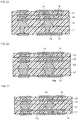
- a modification of the multilayer substrate according to this embodiment is described in further detail with reference to Figs. 14 to 16 each illustrating a multilayer substrate in a manner similar to Fig. 13 .
- Multilayer substrates shown in Figs. 13 to 16 are the multilayer substrates according to the present invention.
- L1 and L2 are inversion layers.
- L3 and L4 correspond to the first thermoplastic resin layers
- L2 corresponds to the second thermoplastic resin layer.
- L1 is the inversion layer, but is not thick. L1 does not correspond to the second thermoplastic resin layer.
- L1 is an inversion layer.
- L3 and L4 correspond to the first thermoplastic resin layers, and L1 corresponds to the second thermoplastic resin layer.
- the second thermoplastic resin layer is not adjacent to the first thermoplastic resin layer in the thickness direction.
- L2 is not an inversion layer, but is thick. L2 does not correspond to the second thermoplastic resin layer.
- L1 and L2 are inversion layers.
- L4 corresponds to the first thermoplastic resin layer
- L2 corresponds to the second thermoplastic resin layer.
- the second thermoplastic resin layer is not adjacent to the first thermoplastic resin layer in the thickness direction.
- L3 is not an inversion layer, but is thick. L3 does not correspond to the second thermoplastic resin layer.
- the second thermoplastic resin layer is preferably arranged at the uppermost layer or the lowermost layer.
- the examples shown in Figs. 13 and 15 correspond to this arrangement.
- the second thermoplastic resin layer is preferably arranged at the uppermost layer or the lowermost layer.
- Arranging the second thermoplastic resin layer at the uppermost layer or the lowermost layer also represents that the thermoplastic resin layer at the uppermost layer or the lowermost layer is thick.
- the in-plane conductive pattern 13 is typically formed of copper foil.
- the in-plane conductive pattern 13 at the uppermost layer or the lowermost layer, i.e., the in-plane conductive pattern 13 that is exposed as the upper or lower surface of the multilayer substrate is typically formed to have a larger surface roughness than the surface roughness of the in-plane conductive pattern 13 in the multilayer substrate, in order to increase bonding strength between the copper foil and the resin layer with use of the rough surface.
- SMD surface mount device
- IC integrated circuit
- back surface Since the lower surface (referred to as “back surface”) of the multilayer substrate is mounted on the motherboard by soldering, high bonding strength is required in order to increase resistance to heat stress during the heat cycle and resistance to drop impact stress.
- Ni/Sn plating, Ni/solder plating, or Ni/Au plating is applied on the copper foil on the upper and lower surfaces of the multilayer substrate.
- Ni plating is in contact with the copper foil, and hence shrinkage stress during plating becomes large. To resist this, the bonding strength between the copper foil and the resin layer is required to be increased.
- the surface roughness of the copper foil that is made rough to increase the bonding strength at the upper and lower surfaces of the multilayer substrate is 10 ⁇ m at the maximum.
- Fig. 17 illustrates such an example. If the thickness of the thermoplastic resin layer 15 is, for example, 25 ⁇ m, the surface projections and depressions of the copper foil of the in-plane conductive pattern 13 dig into the thermoplastic resin layer 15 by about half the thickness of the thermoplastic resin layer 15. The volume of resin of the thermoplastic resin layer 15 at the uppermost layer or the lowermost layer of the multilayer substrate is markedly smaller than the volume of resin of the thermoplastic resin layer 15 at the inner layer of the multilayer substrate. Therefore, the volume of resin (see Figs. 9 to 11 ) flowing to compress the via hole inward is small. To obtain the advantage of the present invention, the thermoplastic resin layer 15 located at the uppermost layer or the lowermost layer is preferably thick.
- the copper foil serving as the in-plane conductive pattern 13 disposed inside the multilayer substrate preferably has a small surface roughness as possible to allow a signal to easily pass through the surface of the copper foil by the skin effect if a high frequency is used.
- the thermoplastic resin layer 15 at the uppermost layer or the lowermost layer is preferably thick.
- the examples in Figs. 13 and 15 are more preferable than the examples in Figs. 14 and 16 from among the modifications shown in Figs. 13 to 16 of the multilayer substrate according to this embodiment.
- the total thickness of the multilayer substrate is decreased as possible and the thickness of the thermoplastic resin layer at the lowermost layer is increased to serve as the second thermoplastic resin layer.
- the example in Fig. 13 is preferable. If the total thickness of the multilayer substrate does not have to be decreased, the example in Fig. 15 can provide the most apparent advantage.
- the example in Fig. 15 from among the examples in Figs. 13 to 16 can most reliably reduce the occurrence of a connection failure between the conductive portions of the respective resin layers at the interface at which the resin layers are arranged in the mutually inverted stacking directions and are in contact with each other.
- a structure, in which two multilayer substrates having multiple layers to increase thicknesses and hence being rigid are connected with each other by a section having a reduced number of layers, is generally called "rigid-flexible substrate.”
- the present invention can be also applied to the rigid-flexible substrate.
- Fig. 18 illustrates an example.
- a rigid-flexible substrate 80 includes rigid sections 81 and a flexible section 82.
- Each of the rigid sections 81 includes four thermoplastic resin layers L1 to L4 in total, thereby being rigid.
- the flexible section 82 includes only a single layer that is the thermoplastic resin layer L2. Hence, the flexible section 82 is easily bent.
- the layer L2 forming the flexible section 82 is continued from the layer L2 included in the rigid sections 81.
- any of the examples in Figs. 14 to 16 may be formed as a rigid-flexible substrate by extending any of the layers L1 to L4.
- the example described here includes the rigid sections having the four layers L1 to L4 in total and the flexible section having the single layer L2 in total.
- the number of thermoplastic resin layers included in the rigid sections may be a number other than four
- the number of thermoplastic resin layers included in the flexible section may be a number other than one.
- the in-plane conducive pattern 13 is preferably metal foil, and the interlayer conductive portion 14 is preferably formed by hardening or low-temperature sintering metal paste filled in a via conductive hole, i.e., a via hole.
- the in-plane conducive pattern 13 is preferably metal foil, and the interlayer conductive portion 14 is preferably formed by hardening or low-temperature sintering metal paste filled in a via conductive hole.
- the in-plane conductive pattern can be in close contact with the resin layer.
- a multilayer substrate 102 according to a second embodiment of the present invention is described with reference to Fig. 19 .
- the basic configuration of the multilayer substrate according to this embodiment is similar to that described in the first embodiment.
- an interlayer conductive portion 14a formed at the second thermoplastic resin layer preferably has a larger diameter than the diameter of the interlayer conductive portion 14 formed at the first thermoplastic resin layer.
- L2 to L4 correspond to the first thermoplastic resin layers
- L1 corresponds to the second thermoplastic resin layer.
- the interlayer conductive portion 14a of L1 that is the second thermoplastic resin layer has the larger diameter than the diameters of the interlayer conductive portions 14 of L2 to L4 that is the first thermoplastic resin layer.
- the second thermoplastic resin layer is thicker than the first thermoplastic resin layer similarly to the configuration described in the first embodiment.
- the resin layer is present as a resin film before stacking.
- the resin film is subjected to various thermal history until the resin film is finished to serve as the multilayer substrate.
- the temperature is 300°C.
- the temperature is 100°C.
- the temperature is 100°C.
- the temperature is in a range from 100°C to 150°C.
- the temperature is in a range from 250°C to 300°C.
- the resin film is thermally deformed in the process of the thermal history.
- the metal paste of the interlayer conductive portion is hardened or sintered at low temperatures, and is bonded to the in-plane conductive pattern.
- Expected forms of thermal deformation of an individual resin film may be a form in which the resin film is expanded or contracted isotropically as shown in Fig. 20 , a form in which the resin film is deformed in a parallelogram as shown in Fig. 21 , and a form in which the resin film is deformed in the other quadrangles as shown in Fig. 22 .
- via holes are present at intersection points on a grating indicated by broken lines, and it is expected that an inverted resin film is overlaid on a non-inverted resin film.
- the shift amount of the intersection points between the two overlaid layers is twice the displacement by which each intersection point is shifted from the initial position.
- the via hole diameter is 100 ⁇ m
- the shift between the inverted and overlaid layers becomes 100 ⁇ m that is twice the value of 50 ⁇ m.
- the shift is substantially as large as the via hole diameter.
- the via holes may not be overlaid on each other. In other words, a condition that causes corresponding via holes at two inverted and overlaid layers to be aligned with each other even by only slightly is as follows: shift amount x ⁇ 50 ⁇ m .
- an effective countermeasure is that the diameter of the interlayer conductive portion at the second thermoplastic resin layer that is to be inverted is larger than the diameter of the interlayer conductive portion formed at the first thermoplastic resin layer.
- the diameter of the interlayer conductive portion formed at the second thermoplastic resin layer is larger than the diameter of the interlayer conductive portion formed at the first thermoplastic resin layer.
- the occurrence of a connection failure can be reduced between the conductive portions of the respective resin layers at the interface at which the resin layers are arranged in the mutually inverted stacking directions and are in contact with each other.
- a configuration in which the diameter of an interlayer conductive portion 14b at a thermoplastic resin layer adjacent to the second thermoplastic resin layer is conceivable as a modification. If the diameter of the interlayer conductive portion 14a at the second thermoplastic resin layer is increased, and the diameter of the interlayer conductive portion 14b at the adjacent layer is increased, this is preferable because the allowable range of the shift amount can be further increased.
- L3 and L4 correspond to the first thermoplastic resin layers
- L1 corresponds to the second thermoplastic resin layer.
- L2 does not correspond to the first thermoplastic resin layer.
- Multilayer substrates shown in Figs. 24 to 31 are the multilayer substrates according to the present invention.
- the thickness of the second thermoplastic resin layer is increased, and the thickness of a thermoplastic resin layer adjacent to the inverted layer in the thickness direction is increased.
- L3 and L4 correspond to the first thermoplastic resin layers
- L1 corresponds to the second thermoplastic resin layer.
- the diameter of the interlayer conductive portion of only one of the two layers of the second thermoplastic resin layer and the thermoplastic resin layer adjacent to the second thermoplastic resin layer may be increased, or the diameters of the interlayer conductive portions at both the two layers may be increased. In each of the examples in Figs.
- the diameter of the interlayer conductive portion 14a of the second thermoplastic resin layer is larger than the diameter of the interlayer conductive portion 14 of the first thermoplastic resin layer according to the second embodiment.
- the diameter of an interlayer conductive portion 14c of the second thermoplastic resin layer is not larger than the diameter of the interlayer conductive portion 14 of the first thermoplastic resin layer.
- Figs. 27 and 28 illustrates an example in which the second thermoplastic resin layer is not located at the lowermost layer but is located at an intermediate layer.
- L3 and L4 correspond to the first thermoplastic resin layers
- L2 corresponds to the second thermoplastic resin layer.
- any of Figs. 29 to 31 illustrates an example in which the structure provided at the lowermost layer and the second layer from the lowermost layer in any of Figs. 24 to 26 is provided by intermediate layers.
- L4 corresponds to the first thermoplastic resin layer
- L2 corresponds to the second thermoplastic resin layer.
- the diameter of the interlayer conductive portion of only one of the two layers of the second thermoplastic resin layer and the thermoplastic resin layer adjacent to the second thermoplastic resin layer, which are present as the intermediate layers of the multilayer substrate may be increased, or the diameters of the interlayer conductive portions of both the two layers may be increased.
- the gap at the interface at which the resin layers are arranged in the mutually inverted stacking directions and are in contact with each other can be reduced or eliminated.
- the allowable range of the shift amount by thermal deformation can be increased.
- the multilayer substrate is configured as the stack including the four thermoplastic resin layers L1 to L4 in total as precondition.
- the number of thermoplastic resin layers forming the multilayer substrate may be a number other than four.
- a multilayer substrate comprises a plurality of stacked thermoplastic resin layers each having an in-plane conductive pattern (13) provided on one of principal surfaces and an interlayer conductive portion (14, 14a, 14b, 14c) provided to penetrate through the thermoplastic resin layer in a thickness direction
- the plurality of thermoplastic resin layers include a first thermoplastic resin layer (15c, 15d, 15e) and a second thermoplastic resin layer (15f) a stacking direction of which is inverted with respect to a stacking direction of the first thermoplastic resin layer, the second thermoplastic resin layer being thicker than the first thermoplastic resin layer, and wherein one of ends in the thickness direction of the interlayer conductive portion formed at the second thermoplastic resin layer is connected with the interlayer conductive portion of the thermoplastic resin layer adjacent to the second thermoplastic resin layer in the thickness direction such that the in-plane conductive pattern is not interposed therebetween.
- the second thermoplastic resin layer is arranged at an uppermost layer or a lowermost layer.
- the interlayer conductive portion formed at the second thermoplastic resin layer has a larger diameter than a diameter of the interlayer conductive portion formed at the first thermoplastic resin layer.
- the interlayer conductive portion of the thermoplastic resin layer connected to the interlayer conductive portion of the second thermoplastic resin layer such that the in-plane conductive pattern is not interposed therebetween has a larger diameter than the diameter of the interlayer conductive portion formed at the first thermoplastic resin layer.
- thermoplastic resin layer connected with the interlayer conductive portion of the second thermoplastic resin layer such that the in-plane conductive pattern is not interposed therebetween is thicker than the first thermoplastic resin layer.
- the in-plane conductive pattern is metal foil
- the interlayer conductive portion is formed by hardening or low-temperature sintering metal paste filled in a via conductor hole.
- a seventh aspect provides a method of manufacturing a multilayer substrate including a plurality of stacked thermoplastic resin layers each having an in-plane conductive pattern (13) provided on one of principal surfaces and an interlayer conductive portion (14, 14a, 14b, 14c) provided to penetrate through the thermoplastic resin layer in a thickness direction, wherein the plurality of thermoplastic resin layers include a first thermoplastic resin layer (15c, 15d, 15e) and a second thermoplastic resin layer (15f) being thicker than the first thermoplastic resin layer, wherein the method comprises a step of stacking the first thermoplastic resin layer, and a step of stacking the second thermoplastic resin layer such that a stacking direction of the second thermoplastic resin layer is inverted with respect to a stacking direction of the first thermoplastic resin layer, and wherein one of ends in the thickness direction of the interlayer conductive portion formed at the second thermoplastic resin layer is connected with the interlayer conductive portion of the thermoplastic resin layer adjacent to the second thermoplastic resin layer in the thickness direction such that the in-plane conductive pattern is
- the second thermoplastic resin layer is arranged at an uppermost layer or a lowermost layer.
- the interlayer conductive portion formed at the second thermoplastic resin layer has a larger diameter than a diameter of the interlayer conductive portion formed at the first thermoplastic resin layer.
- the interlayer conductive portion of the thermoplastic resin layer connected to the interlayer conductive portion of the second thermoplastic resin layer such that the in-plane conductive pattern is not interposed therebetween has a larger diameter than the diameter of the interlayer conductive portion formed at the first thermoplastic resin layer.
- thermoplastic resin layer connected with the interlayer conductive portion of the second thermoplastic resin layer such that the in-plane conductive pattern is not interposed therebetween is thicker than the first thermoplastic resin layer.
- the in-plane conductive pattern is metal foil
- the interlayer conductive portion is formed by hardening or low-temperature sintering metal paste filled in a via conductor hole.
- the present invention can be applied to a multilayer substrate and a manufacturing method thereof.
- Reference Signs List
- thermoplastic resin layer 15c, 15d, 15e thermoplastic resin layer (first thermoplastic resin layer); 15f thermoplastic resin layer (second thermoplastic resin layer); 16 hot plate; 80 rigid-flexible substrate; 81 rigid section; 82 flexible section; 91, 92, 93 arrow; 100, 101, 102 multilayer substrate.
Abstract
Description
- The present invention relates to a multilayer substrate and a manufacturing method thereof.
- An example of the invention relating to a multilayer substrate and a manufacturing method thereof is described in Japanese Unexamined Patent Application Publication No.
2008-147254 -
Fig. 32 illustrates the example of the multilayer substrate described inPTL 1. Thismultilayer substrate 100 includes aninsulated substrate 1 formed by stackingresin films electronic component 2 is held in themultilayer substrate 100 such that theelectronic component 2 is wrapped in theinsulated substrate 1. Each of the resin films has aconductive pattern 3 on only one of principal surfaces. Each of the resin films has aconductive portion 4 therein to penetrate through the resin film in the thickness direction. Theconductive portion 4 is arranged within a region where theconductive pattern 3 extends. Theconductive portion 4 is tapered in cross section. The narrow side is connected with theconductive pattern 3. Hence, when a single resin film is concerned, the wide side of theconductive portion 4 is exposed at another principal surface without theconductive pattern 3. - Referring to
Fig. 32 , theresin films multilayer substrate 100 such that theconductive patterns 3 are arranged at the upper sides. Only theresin film 10f is stacked such that theconductive pattern 3 is arranged at the lower side, to cause theconductive pattern 3 to be exposed at the lowermost surface of themultilayer substrate 100. As described above, the stacking direction of only theresin film 10f is inverted. Theconductive pattern 3 is not present between theresin film 10e and theresin film 10f. Citation List. - PTL 1: Japanese Unexamined Patent Application Publication No.
2008-147254 - Each resin film has the conductive pattern on only one of the principal surfaces inevitably for the convenience of the manufacturing method. The
conductive portion 4 is tapered because the hole is made by laser processing from the surface without theconductive pattern 3 of each resin film. - A mount land electrode has to be provided on the upper surface of the multilayer substrate for mounting a surface mount device (also referred to as "SMD") and an integrated circuit (also referred to as "IC") on the upper surface, and a land electrode has to be provided on the lower surface of the multilayer substrate for mounting the multilayer substrate itself on a motherboard or the other components. In general, when a multilayer substrate is formed by stacking resin films, the stacking direction of either of the uppermost and lowermost resin films has to be inverted to cause conductive patterns to be exposed at both the uppermost and lowermost surfaces.
- In the multilayer substrate thus formed, the
conductive portion 4 of theresin film 10e is directly connected with theconductive portion 4 of theresin film 10f such that theconductive pattern 3 is not interposed therebetween as shown inFig. 32 . However, a connection failure may occur at the connection position between theconductive portions 4. - Accordingly, an object of the present invention is to provide a multilayer substrate and a manufacturing method thereof that can reduce occurrence of a connection failure between conductive portions of respective resin layers at an interface at which the resin layers are arranged in mutually inverted stacking directions and are in contact with each other.
- To attain the above-described object, a multilayer substrate according to the present invention includes a plurality of stacked thermoplastic resin layers each having an in-plane conductive pattern provided on one of principal surfaces and an interlayer conductive portion provided to penetrate through the thermoplastic resin layer in a thickness direction. The plurality of thermoplastic resin layers include a first thermoplastic resin layer and a second thermoplastic resin layer a stacking direction of which is inverted with respect to a stacking direction of the first thermoplastic resin layer, the second thermoplastic resin layer being thicker than the first thermoplastic resin layer. One of ends in the thickness direction of the interlayer conductive portion formed at the second thermoplastic resin layer is connected with the interlayer conductive portion of the thermoplastic resin layer adjacent to the second thermoplastic resin layer in the thickness direction such that the in-plane conductive pattern is not interposed therebetween.
- With the present invention, the occurrence of a connection failure can be reduced between the conductive portions of the respective resin layers at the interface at which the resin layers are arranged in the mutually inverted stacking directions and are in contact with each other.
-
-
Fig. 1 is a cross-sectional view of a state after a resin film is processed by laser processing. -
Fig. 2 is a cross-sectional view of a state after a through hole of the resin film is filled with a conductive material. -
Fig. 3 is a cross-sectional view of a state after a conductive portion provided at the resin film is hardened and shrunk. -
Fig. 4 is an explanatory view of a state in which resin films are stacked. -
Fig. 5 is an explanatory view of a state in which the conductive portion is recessed. -
Fig. 6 is an explanatory view of a state in which the recess of the conductive portion is deformed. -
Fig. 7 is a cross-sectional view of a state in which a gap is trapped in the multilayer substrate. -
Fig. 8 is a cross-sectional view of a multilayer substrate according to a first embodiment of the present invention. -
Fig. 9 is an explanatory view of press-bonding for fabricating the multilayer substrate according to the first embodiment of the present invention. -
Fig. 10 is a partly enlarged cross-sectional view of a single thermoplastic resin layer included in a stack during press-bonding. -
Fig. 11 is an explanatory view of a state in which an interlayer conductive portion protrudes. -
Fig. 12 is a flowchart of a method of manufacturing the multilayer substrate according to the first embodiment of the present invention. -
Fig. 13 is a cross-sectional view of a first example of the multilayer substrate according to the present invention. -
Fig. 14 is a cross-sectional view of a second example of the multilayer substrate according to the present invention. -
Fig. 15 is a cross-sectional view of a third example of the multilayer substrate according to the present invention. -
Fig. 16 is a cross-sectional view of a fourth example of the multilayer substrate according to the present invention. -
Fig. 17 is a cross-sectional view of an area near the upper or lower surface of the multilayer substrate. -
Fig. 18 is a cross-sectional view of an example of a rigid-flexible substrate according to the present invention. -
Fig. 19 is a cross-sectional view of a multilayer substrate according to a second embodiment of the present invention. -
Fig. 20 is an explanatory view of a first form of thermal deformation of a resin film. -
Fig. 21 is an explanatory view of a second form of the thermal deformation of the resin film. -
Fig. 22 is an explanatory view of a third form of the thermal deformation of the resin film. -
Fig. 23 is a cross-sectional view of a modification of the multilayer substrate according to the second embodiment of the present invention. -
Fig. 24 is a cross-sectional view of a first example of the multilayer substrate according to the present invention, in which the thickness of a thermoplastic resin layer adjacent to an inversion layer in the thickness direction is also increased. -
Fig. 25 is a cross-sectional view of a second example of the multilayer substrate according to the present invention, in which the thickness of a thermoplastic resin layer adjacent to an inversion layer in the thickness direction is also increased. -
Fig. 26 is a cross-sectional view of a third example of the multilayer substrate according to the present invention, in which the thickness of a thermoplastic resin layer adjacent to an inversion layer in the thickness direction is also increased. -
Fig. 27 is a cross-sectional view of a first example of the multilayer substrate according to the present invention, in which a second thermoplastic resin layer is positioned as an intermediate layer. -
Fig. 28 is a cross-sectional view of a second example of the multilayer substrate according to the present invention, in which a second thermoplastic resin layer is positioned as an intermediate layer. -
Fig. 29 is a cross-sectional view of a fourth example of the multilayer substrate according to the present invention, in which the thickness of a thermoplastic resin layer adjacent to an inversion layer in the thickness direction is also increased. -
Fig. 30 is a cross-sectional view of a fifth example of the multilayer substrate according to the present invention, in which the thickness of a thermoplastic resin layer adjacent to an inversion layer in the thickness direction is also increased. -
Fig. 31 is a cross-sectional view of a sixth example of the multilayer substrate according to the present invention, in which the thickness of a thermoplastic resin layer adjacent to an inversion layer in the thickness direction is also increased. -
Fig. 32 is a cross-sectional view of a multilayer substrate according to related art. - The inventors have considered as follows for the reason of occurrence of a connection failure between the conductive portions of the respective resin layers at the interface at which the resin layers are arranged in the mutually inverted stacking directions and are in contact with each other as mentioned above.
- Each of the resin films included in the multilayer substrate shown in
Fig. 32 has theconductive portion 4. Laser processing is typically performed to form theconductive portion 4 at the resin film. Specifically, laser light is emitted on the surface without theconductive pattern 3, and as shown inFig. 1 , a tapered throughhole 5 is provided at theresin film 10. Theconductive pattern 3 is exposed at the bottom of the throughhole 5. The throughhole 5 of theresin film 10 is filled with conductive material paste by screen printing or the other methods, thereby providing a structure shown inFig. 2 . That is, aconductive portion 4a is formed. In this state, the structure is dried if required. The conductive material filled as theconductive portion 4a contains resin such as epoxy resin or flux that is liquid in addition to metal components, by several percent to 20% by volume, to increase printability, dispersibility, and wettability, and to harden the material for keeping its shape. The components contained in theconductive portion 4a is partly evaporated through thermal history such as drying, laminating, and heat processing, and theconductive portion 4a itself is hardened and shrunk. Thus, theconductive portion 4a is changed to theconductive portion 4 shown inFig. 3 . When theconductive portion 4a becomes theconductive portion 4, the upper surface of theconductive portion 4 is lower than the upper surface of theresin film 10. Theresin films 10 in such a state are stacked as shown inFig. 32 , applied with heat and pressure, and hence press-bonded. - Illustrating the recess at the exposed surface of the
conductive portion 4 in an exaggerated manner, theresin films 10 are stacked and press-bonded, for example, as shown inFig. 4 . One of the resin films shown inFig. 4 is aresin film 10, and a singleconductive portion 4 included in theresin film 10 is concerned. The thickness of each resin film ranges from about 25 to 50 µm when the resin film is thin. The thickness of theconductive pattern 3 ranges from 10 to 20 µm. Referring toFig. 5 , a depth D by which theconductive portion 4 sinks at the exit side of the throughhole 5 is about 10 µm. - The material of the resin film, or more particularly, thermoplastic resin becomes elasto-plastic, and flows in the horizontal direction while being slightly shrunk in the thickness direction by the heat and pressure during press-bonding. The thermoplastic resin is, for example, liquid crystal polymer (LCP) resin, polyether ether ketone (PEEK) resin, polyether imide (PEI) resin, or polyimide (PI) resin.
- When the thermoplastic resin in the elasto-plastic state flows in the horizontal direction while the thermoplastic resin is slightly shrunk in the thickness direction, copper foil serving as the
conductive pattern 3 is buried into the thermoplastic resin. Meanwhile, theconductive portion 4 is compressed in the horizontal direction by the fluidized thermoplastic resin, and is narrowed inward. Consequently, the recess of theconductive portion 4 shown inFig. 5 becomes small as shown inFig. 6 , and becomes agap 6 at a center part. If thegap 6 of theconductive portion 4 faces and comes into contact with theconductive pattern 3 during stacking, i.e., if thegap 6 is present at any interface among theresin films Fig. 4 , theconductive pattern 3 comes into contact with the recess of theconductive portion 4, and pushes and eliminates thegap 6. - However, if the
gap 6 of theconductive portion 4 does not come into contact with theconductive pattern 3 during stacking, but directly faces and comes into contact with theconductive portion 4 of the other resin films, i.e., if thegap 6 is present between theresin films Fig. 4 , theconductive pattern 3 is not present between theconductive portions 4 and thus thegap 6 is not eliminated. Accordingly, thegap 6 is trapped and remains in the multilayer substrate as shown inFig. 7 . - The remaining
gap 6 may occasionally cause a conduction failure. When the multilayer substrate is mounted on the motherboard by soldering, reflowing is performed. When the multilayer substrate is exposed to high temperatures during reflowing, thegap 6 trapped inside may be expanded and ruptured, and may cause a failure. During wet plating of the multilayer substrate, a plating solution may enter thegap 6, the plating solution may oxidize or dissolve the conductive material or the copper foil serving as theconductive pattern 3, and hence a failure may occur. - At the connection position between the
conductive portions 4 of a contact hole, the area that makes a contribution to electrical connection decreases by the amount of thegap 6. In case of use with a high frequency, conduction resistance increases and hence characteristics may be degraded. - The inventors have considered that the gap remaining in the multilayer substrate causes the connection failure between the conductive portions of the respective layers at the interface at which the resin layers are arranged in the mutually inverted stacking directions and are in contact with each other. Thus, the inventors have made the present invention.
- A multilayer substrate according to a first embodiment of the present invention is described with reference to
Fig. 8 . Amultilayer substrate 101 according to this embodiment includes a plurality of stackedthermoplastic resin layers conductive pattern 13 provided on one of principal surfaces and an interlayerconductive portion 14 provided to penetrate through the thermoplastic resin layer in the thickness direction. The plurality ofthermoplastic resin layers thermoplastic resin layers thermoplastic resin layer 15f the stacking direction of which is inverted with respect to the stacking direction of the firstthermoplastic resin layers thermoplastic resin layer 15f is thicker than the firstthermoplastic resin layers conductive portion 14 formed at the secondthermoplastic resin layer 15f is connected with the interlayerconductive portion 14 of the thermoplastic resin layer 15e adjacent to the secondthermoplastic resin layer 15f in the thickness direction such that the in-planeconductive pattern 13 is not interposed therebetween. - An advantage provided by the multilayer substrate according to this embodiment is described.
- In general, press-bonding for fabricating a multilayer substrate is performed such that
hot plates 16 are arranged above and below stacked thermoplastic resin layers as shown inFig. 9 . To uniformly conduct heat, thehot plates 16 are formed of metal having a high thermal conductivity and likely formed with a high flatness. When pressure is applied in directions indicated byarrows 91, the thermoplastic resin layers tend to escape in the horizontal direction, i.e., in directions indicated byarrows 92. At this time, if the thicknesses of the thermoplastic resin layers are large, the amount of flowing resin increases.Fig. 10 illustrates a singlethermoplastic resin layer 15 included in the stack during press-bonding. If the thickness of thethermoplastic resin layer 15 is large, the amount of resin flowing from the outside to the inside of the interlayerconductive portion 14 in a via hole increases, i.e., the amount of flowing resin so as to compress the interlayerconductive portion 14 in directions indicated byarrows 93 increases. Accordingly, the via hole itself is narrowed inward. Hence, the interlayerconductive portion 14 is pushed out to the exit of the via hole, resulting in that thegap 6 shown inFig. 6 is eliminated. The interlayerconductive portion 14 may pass through the exit of the via hole and may protrude in a direction indicated by anarrow 94 as shown inFig. 11 depending on conditions. In actuality, a via hole of the thermoplastic resin layer 15e adjacent to the secondthermoplastic resin layer 15f is arranged to face the interlayerconductive portion 14 of the secondthermoplastic resin layer 15f having the relatively large thickness in themultilayer substrate 101, at a position to which the interlayerconductive portion 14 of the second thermoplastic resin layer 15e tends to be pushed out. The interlayer conductive portion of the thermoplastic resin layer 15e tends to be pushed out in the facing direction. Hence, the interlayer conductive portions acting in directions in which the interlayer conductive portions are pushed out collide with each other, and closely contact each other. Thus thegap 6 at the interface becomes markedly small or is eliminated. - With this action, the gap at the interface at which the resin layers are arranged in the mutually inverted stacking directions and are in contact with each other can be reduced or eliminated. Accordingly, with this embodiment, the occurrence of a connection failure can be reduced between the conductive portions of the respective resin layers at the interface at which the resin layers are arranged in the mutually inverted stacking directions and are in contact with each other. This advantage noticeably appears as the thickness of the thermoplastic resin layer increases. The second thermoplastic resin layer preferably has a thickness that is 1.5 to 5 times the thickness of the first thermoplastic resin layer in view of the thickness of the multilayer substrate and the advantage.
- The gap can be reduced or eliminated at the interface at which the resin layers are arranged in the mutually inverted stacking direction and are in contact with each other, and at the other interfaces by increasing the thickness of each thermoplastic resin layer. Specifically, by increasing the thermoplastic resin layer having the interlayer
conductive portion 14 that is connected with the in-planeconductive pattern 13, the gap at the interface between the in-planeconductive pattern 13 and the facing interlayerconductive portion 14 can be reduced or eliminated. - In the multilayer substrate according to this embodiment, the occurrence of a connection failure at the interface at which the resin layers are arranged in the mutually inverted stacking direction and are in contact with each other is reduced, and also the conduction resistance is reduced. Accordingly, a high-frequency property is improved. Also, the gap is hardly ruptured during reflowing. Further, since the gap is almost eliminated, the plating solution for wet soldering hardly enters the gap. Accordingly, reliability is improved.
- It is to be noted that the number of stacked thermoplastic resin layers is four in this embodiment; however, the number is not limited to four. The number of stacked resin layers may be the other numbers as long as the number is two or larger.
- The adjacent thermoplastic resin layer 15e is one of the first thermoplastic resin layers, i.e., a thin layer. However, the "adjacent thermoplastic resin layer" is not limited to "one of the first thermoplastic resin layers." The adjacent thermoplastic resin layer may be thick like the second thermoplastic resin layer.
-
Fig. 12 illustrates a flowchart for a method of manufacturing a multilayer substrate according to this embodiment. The method of manufacturing the multilayer substrate according to this embodiment is a method of manufacturing a multilayer substrate including a plurality of stacked thermoplastic resin layers each having an in-plane conductive pattern provided on one of principal surfaces and an interlayer conductive portion provided to penetrate through the thermoplastic resin layer in the thickness direction. The plurality of thermoplastic resin layers include a first thermoplastic resin layer and a second thermoplastic resin layer being thicker than the first thermoplastic resin layer. The method includes a step S1 of stacking the first thermoplastic resin layer, and a step S2 of stacking the second thermoplastic resin layer such that the stacking direction of the second thermoplastic resin layer is inverted with respect to the stacking direction of the first thermoplastic resin layer. One of ends in the thickness direction of the interlayer conductive portion formed at the second thermoplastic resin layer is connected with the interlayer conductive portion of the thermoplastic resin layer adjacent to the second thermoplastic resin layer in the thickness direction such that the in-plane conductive pattern is not interposed therebetween. - With such a manufacturing method, the occurrence of a connection failure can be reduced between the conductive portions of the respective resin layers at the interface at which the resin layers are arranged in the mutually inverted stacking directions and are in contact with each other.
- In the example shown in
Fig. 8 , the lowermost layer is the second thermoplastic resin layer and the other layers are the first thermoplastic resin layers. When it is assumed that the four stacked thermoplastic resin layers are successively called L1 to L4 from the lower side, the resin layers of the example inFig. 8 are expressed as shown inFig. 13 . - When it is assumed that the layer the stacking direction of which is merely inverted is called "inversion layer," in an example shown in
Fig. 13 , a layer L1 that is the lowermost layer corresponds to the inversion layer. However, the position of the inversion layer is not limited to the lowermost layer in the multilayer substrate according to the present invention. The inversion layer may be the uppermost layer or an intermediate layer. Also, the number of inversion layers is not limited to one in the multilayer substrate according to the present invention. The number of inversion layers may be a plural number. In this case, all inversion layers do not have to be the second thermoplastic resin layers. - The first thermoplastic resin layer is any of layers stacked to form a multilayer substrate. In contrast, the second thermoplastic resin layer satisfies all three requirements described below.
- (1) The stacking direction of the second thermoplastic resin layer is inverted with respect to the stacking direction of the first thermoplastic resin layer.
- (2) The second thermoplastic resin layer is thicker than the first thermoplastic resin layer.
- (3) One of ends in the thickness direction of the interlayer conductive portion of the second thermoplastic resin layer is connected with the interlayer conductive portion of either of thermoplastic resin layers adjacent to the second thermoplastic resin layer in the thickness direction such that the in-plane conductive pattern is not interposed therebetween.
- The multilayer substrate according to the present invention includes the plurality of thermoplastic resin layers which form the multilayer substrate and include the first and second thermoplastic resin layers that satisfy the requirements. The multilayer substrate may include a thermoplastic resin layer that is none of the first and second thermoplastic resin layers. A modification of the multilayer substrate according to this embodiment is described in further detail with reference to
Figs. 14 to 16 each illustrating a multilayer substrate in a manner similar toFig. 13 . Multilayer substrates shown inFigs. 13 to 16 are the multilayer substrates according to the present invention. - In an example in
Fig. 14 , L1 and L2 are inversion layers. L3 and L4 correspond to the first thermoplastic resin layers, and L2 corresponds to the second thermoplastic resin layer. L1 is the inversion layer, but is not thick. L1 does not correspond to the second thermoplastic resin layer. - In an example in
Fig. 15 , L1 is an inversion layer. L3 and L4 correspond to the first thermoplastic resin layers, and L1 corresponds to the second thermoplastic resin layer. In this case, the second thermoplastic resin layer is not adjacent to the first thermoplastic resin layer in the thickness direction. L2 is not an inversion layer, but is thick. L2 does not correspond to the second thermoplastic resin layer. - In an example in
Fig. 16 , L1 and L2 are inversion layers. L4 corresponds to the first thermoplastic resin layer, and L2 corresponds to the second thermoplastic resin layer. In this case, the second thermoplastic resin layer is not adjacent to the first thermoplastic resin layer in the thickness direction. L3 is not an inversion layer, but is thick. L3 does not correspond to the second thermoplastic resin layer. - For the multilayer substrate according to this embodiment, the second thermoplastic resin layer is preferably arranged at the uppermost layer or the lowermost layer. The examples shown in
Figs. 13 and 15 correspond to this arrangement. - For the method of manufacturing the multilayer substrate according to this embodiment, the second thermoplastic resin layer is preferably arranged at the uppermost layer or the lowermost layer.
- Arranging the second thermoplastic resin layer at the uppermost layer or the lowermost layer also represents that the thermoplastic resin layer at the uppermost layer or the lowermost layer is thick.
- The in-plane
conductive pattern 13 is typically formed of copper foil. The in-planeconductive pattern 13 at the uppermost layer or the lowermost layer, i.e., the in-planeconductive pattern 13 that is exposed as the upper or lower surface of the multilayer substrate is typically formed to have a larger surface roughness than the surface roughness of the in-planeconductive pattern 13 in the multilayer substrate, in order to increase bonding strength between the copper foil and the resin layer with use of the rough surface. - Since the surface mount device (SMD) and the integrated circuit (IC) are mounted on the upper surface (referred to as "front surface") of the multilayer substrate by soldering, bonding strength that is strong enough to resist shrinkage stress of solder is required between the copper foil and the resin layer. The main material of SMD is typically ceramic. The main material of IC is Si. These materials have thermal expansion coefficients different from that of the resin layer. A thermal stress is generated during heat cycle. Hence, high bonding strength that is enough to resist the heat stress is required between the copper foil and the resin layer.
- Since the lower surface (referred to as "back surface") of the multilayer substrate is mounted on the motherboard by soldering, high bonding strength is required in order to increase resistance to heat stress during the heat cycle and resistance to drop impact stress.
- For easy soldering, Ni/Sn plating, Ni/solder plating, or Ni/Au plating is applied on the copper foil on the upper and lower surfaces of the multilayer substrate. Ni plating is in contact with the copper foil, and hence shrinkage stress during plating becomes large. To resist this, the bonding strength between the copper foil and the resin layer is required to be increased.
- The surface roughness of the copper foil that is made rough to increase the bonding strength at the upper and lower surfaces of the multilayer substrate is 10 µm at the maximum.
Fig. 17 illustrates such an example. If the thickness of thethermoplastic resin layer 15 is, for example, 25 µm, the surface projections and depressions of the copper foil of the in-planeconductive pattern 13 dig into thethermoplastic resin layer 15 by about half the thickness of thethermoplastic resin layer 15. The volume of resin of thethermoplastic resin layer 15 at the uppermost layer or the lowermost layer of the multilayer substrate is markedly smaller than the volume of resin of thethermoplastic resin layer 15 at the inner layer of the multilayer substrate. Therefore, the volume of resin (seeFigs. 9 to 11 ) flowing to compress the via hole inward is small. To obtain the advantage of the present invention, thethermoplastic resin layer 15 located at the uppermost layer or the lowermost layer is preferably thick. - In contrast, the copper foil serving as the in-plane
conductive pattern 13 disposed inside the multilayer substrate preferably has a small surface roughness as possible to allow a signal to easily pass through the surface of the copper foil by the skin effect if a high frequency is used. - As described above, the
thermoplastic resin layer 15 at the uppermost layer or the lowermost layer is preferably thick. The examples inFigs. 13 and 15 are more preferable than the examples inFigs. 14 and 16 from among the modifications shown inFigs. 13 to 16 of the multilayer substrate according to this embodiment. In the example inFig. 13 , the total thickness of the multilayer substrate is decreased as possible and the thickness of the thermoplastic resin layer at the lowermost layer is increased to serve as the second thermoplastic resin layer. Hence, the example inFig. 13 is preferable. If the total thickness of the multilayer substrate does not have to be decreased, the example inFig. 15 can provide the most apparent advantage. In other words, the example inFig. 15 from among the examples inFigs. 13 to 16 can most reliably reduce the occurrence of a connection failure between the conductive portions of the respective resin layers at the interface at which the resin layers are arranged in the mutually inverted stacking directions and are in contact with each other. - A structure, in which two multilayer substrates having multiple layers to increase thicknesses and hence being rigid are connected with each other by a section having a reduced number of layers, is generally called "rigid-flexible substrate." The present invention can be also applied to the rigid-flexible substrate.
Fig. 18 illustrates an example. A rigid-flexible substrate 80 includesrigid sections 81 and aflexible section 82. Each of therigid sections 81 includes four thermoplastic resin layers L1 to L4 in total, thereby being rigid. Theflexible section 82 includes only a single layer that is the thermoplastic resin layer L2. Hence, theflexible section 82 is easily bent. The layer L2 forming theflexible section 82 is continued from the layer L2 included in therigid sections 81. The example shown inFig. 18 is the rigid-flexible substrate formed by extending the layer L2 of the example shown inFig. 13 . Alternatively, any of the examples inFigs. 14 to 16 may be formed as a rigid-flexible substrate by extending any of the layers L1 to L4. - The example described here includes the rigid sections having the four layers L1 to L4 in total and the flexible section having the single layer L2 in total. However, the number of thermoplastic resin layers included in the rigid sections may be a number other than four, and the number of thermoplastic resin layers included in the flexible section may be a number other than one.
- In the multilayer substrate according to this embodiment, the in-plane
conducive pattern 13 is preferably metal foil, and the interlayerconductive portion 14 is preferably formed by hardening or low-temperature sintering metal paste filled in a via conductive hole, i.e., a via hole. In the method of manufacturing the multilayer substrate according to this embodiment, the in-planeconducive pattern 13 is preferably metal foil, and the interlayerconductive portion 14 is preferably formed by hardening or low-temperature sintering metal paste filled in a via conductive hole. - This configuration facilitates the fabrication. Also, since the metal foil forms the in-plane conductive pattern, the in-plane conductive pattern can be in close contact with the resin layer.
- A
multilayer substrate 102 according to a second embodiment of the present invention is described with reference toFig. 19 . The basic configuration of the multilayer substrate according to this embodiment is similar to that described in the first embodiment. In themultilayer substrate 102 according to this embodiment, an interlayerconductive portion 14a formed at the second thermoplastic resin layer preferably has a larger diameter than the diameter of the interlayerconductive portion 14 formed at the first thermoplastic resin layer. In the example shown inFig. 19 , L2 to L4 correspond to the first thermoplastic resin layers, and L1 corresponds to the second thermoplastic resin layer. The interlayerconductive portion 14a of L1 that is the second thermoplastic resin layer has the larger diameter than the diameters of the interlayerconductive portions 14 of L2 to L4 that is the first thermoplastic resin layer. Also in this embodiment, the second thermoplastic resin layer is thicker than the first thermoplastic resin layer similarly to the configuration described in the first embodiment. - An advantage provided by the multilayer substrate according to this embodiment is described. In this embodiment, first, the advantage described in the first embodiment can be obtained. In addition, an advantage can be obtained for a shift caused by thermal deformation. This point is described below.
- The resin layer is present as a resin film before stacking. The resin film is subjected to various thermal history until the resin film is finished to serve as the multilayer substrate. For example, when the resin film is bonded to the copper foil that becomes the in-plane conductive pattern, the temperature is 300°C. When a photoresist film is attached for patterning the copper foil, the temperature is 100°C. During drying after etching of the copper foil, the temperature is 100°C. During drying after the inside of the via hole is filled with the conductive member, the temperature is in a range from 100°C to 150°C. During press-bonding of the stack, the temperature is in a range from 250°C to 300°C. The resin film is thermally deformed in the process of the thermal history. At the same time, the metal paste of the interlayer conductive portion is hardened or sintered at low temperatures, and is bonded to the in-plane conductive pattern.
- Expected forms of thermal deformation of an individual resin film may be a form in which the resin film is expanded or contracted isotropically as shown in
Fig. 20 , a form in which the resin film is deformed in a parallelogram as shown inFig. 21 , and a form in which the resin film is deformed in the other quadrangles as shown inFig. 22 . Herein, it is assumed that via holes are present at intersection points on a grating indicated by broken lines, and it is expected that an inverted resin film is overlaid on a non-inverted resin film. - In the case of the isotropic expansion or contraction as shown in
Fig. 20 , the positions of the intersection points at the respective layers are not shifted from each other even when the resin layer is inverted and overlaid. However, in the case of the deformation shown inFig. 21 , the intersection points are shifted from each other when the resin layer is inverted and overlaid. If a certain intersection point is shifted by +x as the result of deformation from the position before the deformation, the shift of the intersection point at the inverted layer appears as -x. When the inverted layer is overlaid on the non-inverted layer, the shift between the corresponding intersection points becomes (+x) - (-x) = +2x. That is, the shift amount of the intersection points between the two overlaid layers is twice the displacement by which each intersection point is shifted from the initial position. For example, in a case in which the via hole diameter is 100 µm, if a certain intersection point is shifted from the initial position by 50 µm as the result of the deformation as shown inFig. 21 , the shift between the inverted and overlaid layers becomes 100 µm that is twice the value of 50 µm. The shift is substantially as large as the via hole diameter. The via holes may not be overlaid on each other. In other words, a condition that causes corresponding via holes at two inverted and overlaid layers to be aligned with each other even by only slightly is as follows:
- As described in this embodiment, an effective countermeasure is that the diameter of the interlayer conductive portion at the second thermoplastic resin layer that is to be inverted is larger than the diameter of the interlayer conductive portion formed at the first thermoplastic resin layer. For example, if the diameter of the interlayer conductive portion at the first thermoplastic resin layer is 100 µm and the diameter of the interlayer conductive portion at the second thermoplastic resin layer is 200 µm, and if the first thermoplastic resin layer is directly overlaid on the second thermoplastic resin layer, a condition that causes corresponding via holes in the two inverted and overlaid layers to be aligned with each other even by only slightly is as follows:

- In the method of manufacturing the multilayer substrate according to this embodiment, the diameter of the interlayer conductive portion formed at the second thermoplastic resin layer is larger than the diameter of the interlayer conductive portion formed at the first thermoplastic resin layer.
- With such a manufacturing method, the occurrence of a connection failure can be reduced between the conductive portions of the respective resin layers at the interface at which the resin layers are arranged in the mutually inverted stacking directions and are in contact with each other.
- As shown in
Fig. 23 , a configuration in which the diameter of an interlayerconductive portion 14b at a thermoplastic resin layer adjacent to the second thermoplastic resin layer is conceivable as a modification. If the diameter of the interlayerconductive portion 14a at the second thermoplastic resin layer is increased, and the diameter of the interlayerconductive portion 14b at the adjacent layer is increased, this is preferable because the allowable range of the shift amount can be further increased. In the example shown inFig. 23 , L3 and L4 correspond to the first thermoplastic resin layers, and L1 corresponds to the second thermoplastic resin layer. L2 does not correspond to the first thermoplastic resin layer. - A modification of the multilayer substrate according to this embodiment is described in further detail with reference to
Figs. 24 to 31 each illustrating a multilayer substrate in a manner similar toFig. 13 . Multilayer substrates shown inFigs. 24 to 31 are the multilayer substrates according to the present invention. - In the examples shown in
Figs. 24 to 26 , the thickness of the second thermoplastic resin layer is increased, and the thickness of a thermoplastic resin layer adjacent to the inverted layer in the thickness direction is increased. In any of the examples shown inFigs. 24 to 26 , L3 and L4 correspond to the first thermoplastic resin layers, and L1 corresponds to the second thermoplastic resin layer. According to the present invention, as shown inFigs. 24 to 26 , the diameter of the interlayer conductive portion of only one of the two layers of the second thermoplastic resin layer and the thermoplastic resin layer adjacent to the second thermoplastic resin layer may be increased, or the diameters of the interlayer conductive portions at both the two layers may be increased. In each of the examples inFigs. 24 and26 , the diameter of the interlayerconductive portion 14a of the second thermoplastic resin layer is larger than the diameter of the interlayerconductive portion 14 of the first thermoplastic resin layer according to the second embodiment. In the example inFig. 25 , the diameter of an interlayerconductive portion 14c of the second thermoplastic resin layer is not larger than the diameter of the interlayerconductive portion 14 of the first thermoplastic resin layer. Hence this example does not correspond to the configuration described in the second embodiment. However, this example corresponds to the configuration described in the first embodiment. - Any of
Figs. 27 and28 illustrates an example in which the second thermoplastic resin layer is not located at the lowermost layer but is located at an intermediate layer. In any of the examples shown inFigs. 27 and28 , L3 and L4 correspond to the first thermoplastic resin layers, and L2 corresponds to the second thermoplastic resin layer. - Any of
Figs. 29 to 31 illustrates an example in which the structure provided at the lowermost layer and the second layer from the lowermost layer in any ofFigs. 24 to 26 is provided by intermediate layers. In any of the examples shown inFigs. 29 to 31 , L4 corresponds to the first thermoplastic resin layer, and L2 corresponds to the second thermoplastic resin layer. According to the present invention, as shown inFigs. 29 to 31 , the diameter of the interlayer conductive portion of only one of the two layers of the second thermoplastic resin layer and the thermoplastic resin layer adjacent to the second thermoplastic resin layer, which are present as the intermediate layers of the multilayer substrate, may be increased, or the diameters of the interlayer conductive portions of both the two layers may be increased. - Even with these modifications, the gap at the interface at which the resin layers are arranged in the mutually inverted stacking directions and are in contact with each other can be reduced or eliminated. In addition, the allowable range of the shift amount by thermal deformation can be increased.
- In any of the above-described embodiments, the multilayer substrate is configured as the stack including the four thermoplastic resin layers L1 to L4 in total as precondition. However, the number of thermoplastic resin layers forming the multilayer substrate may be a number other than four.
- The embodiments disclosed in this description are merely examples and do not intend to limit the present invention. The scope of the present invention is not determined by the above description but is determined by the claims, and includes all modifications within the equivalent meaning and scope of the claims.
- In a first aspect, a multilayer substrate comprises a plurality of stacked thermoplastic resin layers each having an in-plane conductive pattern (13) provided on one of principal surfaces and an interlayer conductive portion (14, 14a, 14b, 14c) provided to penetrate through the thermoplastic resin layer in a thickness direction,
wherein the plurality of thermoplastic resin layers include a first thermoplastic resin layer (15c, 15d, 15e) and a second thermoplastic resin layer (15f) a stacking direction of which is inverted with respect to a stacking direction of the first thermoplastic resin layer, the second thermoplastic resin layer being thicker than the first thermoplastic resin layer, and
wherein one of ends in the thickness direction of the interlayer conductive portion formed at the second thermoplastic resin layer is connected with the interlayer conductive portion of the thermoplastic resin layer adjacent to the second thermoplastic resin layer in the thickness direction such that the in-plane conductive pattern is not interposed therebetween. - In a second aspect, in the multilayer substrate according to the first aspect, the second thermoplastic resin layer is arranged at an uppermost layer or a lowermost layer.
- In a third aspect, in the multilayer substrate according to the first aspect, the interlayer conductive portion formed at the second thermoplastic resin layer has a larger diameter than a diameter of the interlayer conductive portion formed at the first thermoplastic resin layer.
- In a fourth aspect, in the multilayer substrate according to any of first to third aspects, the interlayer conductive portion of the thermoplastic resin layer connected to the interlayer conductive portion of the second thermoplastic resin layer such that the in-plane conductive pattern is not interposed therebetween has a larger diameter than the diameter of the interlayer conductive portion formed at the first thermoplastic resin layer.
- In a fifth aspect, in the multilayer substrate according to any of the first to fourth aspects, the thermoplastic resin layer connected with the interlayer conductive portion of the second thermoplastic resin layer such that the in-plane conductive pattern is not interposed therebetween is thicker than the first thermoplastic resin layer.
- In a sixth aspect, in the multilayer substrate according to any of the first to fifth aspects, the in-plane conductive pattern is metal foil, and the interlayer conductive portion is formed by hardening or low-temperature sintering metal paste filled in a via conductor hole.
- A seventh aspect provides a method of manufacturing a multilayer substrate including a plurality of stacked thermoplastic resin layers each having an in-plane conductive pattern (13) provided on one of principal surfaces and an interlayer conductive portion (14, 14a, 14b, 14c) provided to penetrate through the thermoplastic resin layer in a thickness direction,
wherein the plurality of thermoplastic resin layers include a first thermoplastic resin layer (15c, 15d, 15e) and a second thermoplastic resin layer (15f) being thicker than the first thermoplastic resin layer,
wherein the method comprises
a step of stacking the first thermoplastic resin layer, and
a step of stacking the second thermoplastic resin layer such that a stacking direction of the second thermoplastic resin layer is inverted with respect to a stacking direction of the first thermoplastic resin layer, and
wherein one of ends in the thickness direction of the interlayer conductive portion formed at the second thermoplastic resin layer is connected with the interlayer conductive portion of the thermoplastic resin layer adjacent to the second thermoplastic resin layer in the thickness direction such that the in-plane conductive pattern is not interposed therebetween. - In an eighth aspect, in the method of manufacturing the multilayer substrate according to the seventh aspect, the second thermoplastic resin layer is arranged at an uppermost layer or a lowermost layer.
- In a ninth aspect, in the method of manufacturing the multilayer substrate according to the seventh aspect, the interlayer conductive portion formed at the second thermoplastic resin layer has a larger diameter than a diameter of the interlayer conductive portion formed at the first thermoplastic resin layer.
- In a tenth aspect, in the method of manufacturing the multilayer substrate according to any one of the seventh to ninth aspects, the interlayer conductive portion of the thermoplastic resin layer connected to the interlayer conductive portion of the second thermoplastic resin layer such that the in-plane conductive pattern is not interposed therebetween has a larger diameter than the diameter of the interlayer conductive portion formed at the first thermoplastic resin layer.
- In an eleventh aspect, in the method of manufacturing the multilayer substrate according to any one of the seventh to tenth aspects, the thermoplastic resin layer connected with the interlayer conductive portion of the second thermoplastic resin layer such that the in-plane conductive pattern is not interposed therebetween is thicker than the first thermoplastic resin layer.
- In a twelfth aspect, in the method of manufacturing the multilayer substrate according to any one of the seventh to tenth aspects, the in-plane conductive pattern is metal foil, and the interlayer conductive portion is formed by hardening or low-temperature sintering metal paste filled in a via conductor hole.
- The present invention can be applied to a multilayer substrate and a manufacturing method thereof. Reference Signs List
- 1 insulated substrate; 2 electronic component; 3 conductive pattern; 4, 4a conductive portion; 5 through hole; 6 gap; 10, 10a, 10b, 10c, 10d, 10e, 10f resin film; 13 in-plane conductive pattern, 14, 14a, 14b, 14c interlayer conductive portion; 15 thermoplastic resin layer; 15c, 15d, 15e thermoplastic resin layer (first thermoplastic resin layer); 15f thermoplastic resin layer (second thermoplastic resin layer); 16 hot plate; 80 rigid-flexible substrate; 81 rigid section; 82 flexible section; 91, 92, 93 arrow; 100, 101, 102 multilayer substrate.
Claims (12)
- A multilayer substrate comprising a plurality of stacked heat-press-bonded thermoplastic resin layers each having an in-plane conductive pattern (13) provided on one of principal surfaces and an interlayer conductive portion (14, 14a, 14b, 14c) provided to penetrate through the thermoplastic resin layer in a thickness direction,
wherein the plurality of thermoplastic resin layers include a first thermoplastic resin layer (15c, 15d, 15e) and a second thermoplastic resin layer (15f) a stacking direction of which is inverted with respect to a stacking direction of the first thermoplastic resin layer, the second thermoplastic resin layer being thicker than the first thermoplastic resin layer,
wherein one of ends in the thickness direction of the interlayer conductive portion formed at the second thermoplastic resin layer is connected with the interlayer conductive portion of the thermoplastic resin layer adjacent to the second thermoplastic resin layer in the thickness direction such that the in-plane conductive pattern is not interposed therebetween, and
wherein the interlayer conductive portion formed at the second thermoplastic resin layer has a larger diameter than a diameter of the interlayer conductive portion formed at the first thermoplastic resin layer. - A multilayer substrate comprising a plurality of stacked heat-press-bonded thermoplastic resin layers each having an in-plane conductive pattern (13) provided on one of principal surfaces and an interlayer conductive portion (14, 14a, 14b, 14c) provided to penetrate through the thermoplastic resin layer in a thickness direction,
wherein the plurality of thermoplastic resin layers include a first thermoplastic resin layer (15c, 15d, 15e) and a second thermoplastic resin layer (15f) a stacking direction of which is inverted with respect to a stacking direction of the first thermoplastic resin layer, the second thermoplastic resin layer being thicker than the first thermoplastic resin layer, and
wherein one of ends in the thickness direction of the interlayer conductive portion formed at the second thermoplastic resin layer is connected with the interlayer conductive portion of the thermoplastic resin layer adjacent to the second thermoplastic resin layer in the thickness direction such that the in-plane conductive pattern is not interposed therebetween,
wherein the interlayer conductive portion of the thermoplastic resin layer connected to the interlayer conductive portion of the second thermoplastic resin layer such that the in-plane conductive pattern is not interposed therebetween has a larger diameter than the diameter of the interlayer conductive portion formed at the first thermoplastic resin layer. - The multilayer substrate according to claim 1 or 2, wherein the second thermoplastic resin layer is arranged at an uppermost layer or a lowermost layer.
- The multilayer substrate according to any of claims 1 to 3, wherein the thermoplastic resin layer connected with the interlayer conductive portion of the second thermoplastic resin layer such that the in-plane conductive pattern is not interposed therebetween is thicker than the first thermoplastic resin layer.
- The multilayer substrate according to any of claims 1 to 4, wherein the in-plane conductive pattern is metal foil, and the interlayer conductive portion is formed by hardening or low-temperature sintering metal paste filled in a via conductor hole.
- The multilayer substrate according to any of claims 1 to 5, wherein the interlayer conductive portions are formed by filling a tapered through hole (5).
- A method of manufacturing a multilayer substrate including a plurality of stacked thermoplastic resin layers each having an in-plane conductive pattern (13) provided on one of principal surfaces and an interlayer conductive portion (14, 14a, 14b, 14c) provided to penetrate through the thermoplastic resin layer in a thickness direction,
wherein the plurality of thermoplastic resin layers include a first thermoplastic resin layer (15c, 15d, 15e) and a second thermoplastic resin layer (15f) being thicker than the first thermoplastic resin layer,
wherein the method comprises
a step of stacking the first thermoplastic resin layer, and
a step of stacking the second thermoplastic resin layer such that a stacking direction of the second thermoplastic resin layer is inverted with respect to a stacking direction of the first thermoplastic resin layer, and
wherein one of ends in the thickness direction of the interlayer conductive portion formed at the second thermoplastic resin layer is connected with the interlayer conductive portion of the thermoplastic resin layer adjacent to the second thermoplastic resin layer in the thickness direction such that the in-plane conductive pattern is not interposed therebetween, and
press bonding the stacked thermoplastic resin layers by applying heat and pressure,
wherein the interlayer conductive portion formed at the second thermoplastic resin layer has a larger diameter than a diameter of the interlayer conductive portion formed at the first thermoplastic resin layer. - A method of manufacturing a multilayer substrate including a plurality of stacked thermoplastic resin layers each having an in-plane conductive pattern (13) provided on one of principal surfaces and an interlayer conductive portion (14, 14a, 14b, 14c) provided to penetrate through the thermoplastic resin layer in a thickness direction,
wherein the plurality of thermoplastic resin layers include a first thermoplastic resin layer (15c, 15d, 15e) and a second thermoplastic resin layer (15f) being thicker than the first thermoplastic resin layer,
wherein the method comprises
a step of stacking the first thermoplastic resin layer, and
a step of stacking the second thermoplastic resin layer such that a stacking direction of the second thermoplastic resin layer is inverted with respect to a stacking direction of the first thermoplastic resin layer, and
wherein one of ends in the thickness direction of the interlayer conductive portion formed at the second thermoplastic resin layer is connected with the interlayer conductive portion of the thermoplastic resin layer adjacent to the second thermoplastic resin layer in the thickness direction such that the in-plane conductive pattern is not interposed therebetween,
press bonding the stacked thermoplastic resin layers by applying heat and pressure,
wherein the interlayer conductive portion of the thermoplastic resin layer connected to the interlayer conductive portion of the second thermoplastic resin layer such that the in-plane conductive pattern is not interposed therebetween has a larger diameter than the diameter of the interlayer conductive portion formed at the first thermoplastic resin layer. - The method of manufacturing the multilayer substrate according to claim 7 or 8, wherein the second thermoplastic resin layer is arranged at an uppermost layer or a lowermost layer.
- The method of manufacturing the multilayer substrate according to any of claims 7 to 9, wherein the thermoplastic resin layer connected with the interlayer conductive portion of the second thermoplastic resin layer such that the in-plane conductive pattern is not interposed therebetween is thicker than the first thermoplastic resin layer.
- The method of manufacturing the multilayer substrate according to any of claims 7 to 10, wherein the in-plane conductive pattern is metal foil, and the interlayer conductive portion is formed by hardening or low-temperature sintering metal paste filled in a via conductor hole.
- The method according to any of claims 8 to 11, wherein the interlayer conductive portions (14, 14a, 14b, 14c) are formed by filling a tapered through hole (5).
Applications Claiming Priority (3)
| Application Number | Priority Date | Filing Date | Title |
|---|---|---|---|
| JP2009257185 | 2009-11-10 | ||
| EP10829897.7A EP2475235B1 (en) | 2009-11-10 | 2010-11-08 | Multilayer board and manufacturing method thereof |
| PCT/JP2010/069797 WO2011058938A1 (en) | 2009-11-10 | 2010-11-08 | Multilayer board and manufacturing method thereof |
Related Parent Applications (2)
| Application Number | Title | Priority Date | Filing Date |
|---|---|---|---|
| EP10829897.7A Division-Into EP2475235B1 (en) | 2009-11-10 | 2010-11-08 | Multilayer board and manufacturing method thereof |
| EP10829897.7A Division EP2475235B1 (en) | 2009-11-10 | 2010-11-08 | Multilayer board and manufacturing method thereof |
Publications (1)
| Publication Number | Publication Date |
|---|---|
| EP3570649A1 true EP3570649A1 (en) | 2019-11-20 |
Family
ID=43991597
Family Applications (2)
| Application Number | Title | Priority Date | Filing Date |
|---|---|---|---|
| EP10829897.7A Active EP2475235B1 (en) | 2009-11-10 | 2010-11-08 | Multilayer board and manufacturing method thereof |
| EP19184242.6A Pending EP3570649A1 (en) | 2009-11-10 | 2010-11-08 | Multilayer board and manufacturing method thereof |
Family Applications Before (1)
| Application Number | Title | Priority Date | Filing Date |
|---|---|---|---|
| EP10829897.7A Active EP2475235B1 (en) | 2009-11-10 | 2010-11-08 | Multilayer board and manufacturing method thereof |
Country Status (5)
| Country | Link |
|---|---|
| US (1) | US8604349B2 (en) |
| EP (2) | EP2475235B1 (en) |
| JP (1) | JP5024484B2 (en) |
| CN (1) | CN102598887B (en) |
| WO (1) | WO2011058938A1 (en) |
Families Citing this family (13)
| Publication number | Priority date | Publication date | Assignee | Title |
|---|---|---|---|---|
| KR101397303B1 (en) * | 2012-12-31 | 2014-05-23 | 삼성전기주식회사 | Printed circuit board and method for manufacturing the same |
| TWI565378B (en) * | 2012-12-31 | 2017-01-01 | 三星電機股份有限公司 | Circuit board and method of manufacturing the same |
| JP5842859B2 (en) * | 2013-04-15 | 2016-01-13 | 株式会社村田製作所 | Multilayer wiring board and module having the same |
| WO2017026208A1 (en) * | 2015-08-10 | 2017-02-16 | 株式会社村田製作所 | Resin multilayer substrate and method for manufacturing same |
| CN209517682U (en) * | 2016-05-19 | 2019-10-18 | 株式会社村田制作所 | Multilager base plate |
| JP2019009244A (en) * | 2017-06-23 | 2019-01-17 | 三星ダイヤモンド工業株式会社 | Cutting method of multilayer substrate |
| WO2019044425A1 (en) | 2017-08-30 | 2019-03-07 | 株式会社村田製作所 | Multilayer substrate and antenna module |
| JP7004004B2 (en) * | 2017-10-26 | 2022-01-21 | 株式会社村田製作所 | Multilayer boards, interposers and electronic devices |
| JP7075785B2 (en) * | 2018-03-08 | 2022-05-26 | スタンレー電気株式会社 | Circuit boards, electronic circuit devices, and methods for manufacturing circuit boards |
| CN215991352U (en) | 2019-03-29 | 2022-03-08 | 株式会社村田制作所 | Resin multilayer substrate |
| CN219204859U (en) | 2020-06-03 | 2023-06-16 | 株式会社村田制作所 | Multilayer substrate |
| WO2022244335A1 (en) * | 2021-05-21 | 2022-11-24 | 株式会社村田製作所 | Electronic component and method for manufacturing same |
| WO2023135931A1 (en) * | 2022-01-13 | 2023-07-20 | 株式会社村田製作所 | Multilayer substrate |
Citations (3)
| Publication number | Priority date | Publication date | Assignee | Title |
|---|---|---|---|---|
| US20040037966A1 (en) * | 2002-07-03 | 2004-02-26 | Tomohiro Yokochi | Protective film for base substrates of multi-layered board and method and apparatus for inspecting base substrates |
| JP2006210533A (en) * | 2005-01-26 | 2006-08-10 | Komatsu Lite Seisakusho:Kk | Multilayer printed board and its manufacturing method |
| JP2008147254A (en) | 2006-12-06 | 2008-06-26 | Denso Corp | Multilayer substrate, and method for manufacturing multilayer substrate |
Family Cites Families (14)
| Publication number | Priority date | Publication date | Assignee | Title |
|---|---|---|---|---|
| JP3926064B2 (en) * | 1999-06-30 | 2007-06-06 | 大日本印刷株式会社 | Printed wiring board and method for manufacturing printed wiring board |
| JP4486196B2 (en) * | 1999-12-08 | 2010-06-23 | イビデン株式会社 | Single-sided circuit board for multilayer printed wiring board and manufacturing method thereof |
| JP2002305382A (en) | 2001-02-05 | 2002-10-18 | Denso Corp | Printed board and manufacturing method thereof |
| JP4181778B2 (en) * | 2002-02-05 | 2008-11-19 | ソニー株式会社 | Wiring board manufacturing method |
| JP3820415B2 (en) * | 2002-03-07 | 2006-09-13 | 株式会社デンソー | Printed circuit board manufacturing method and printed circuit board structure |
| JP2003311500A (en) | 2002-04-23 | 2003-11-05 | Denso Corp | Hot press method and hot press |
| JP2004127970A (en) * | 2002-09-30 | 2004-04-22 | Denso Corp | Method for producing elemental board of multilayer board and method for producing multilayer board using that elemental board |
| JP4121354B2 (en) * | 2002-10-28 | 2008-07-23 | 株式会社フジクラ | Wiring substrate base material and method for producing multilayer wiring substrate base material |
| JP4029759B2 (en) * | 2003-04-04 | 2008-01-09 | 株式会社デンソー | Multilayer circuit board and manufacturing method thereof |
| TW200505304A (en) * | 2003-05-20 | 2005-02-01 | Matsushita Electric Ind Co Ltd | Multilayer circuit board and method for manufacturing the same |
| JP2006073763A (en) | 2004-09-01 | 2006-03-16 | Denso Corp | Manufacturing method for multilayer board |
| JP4699136B2 (en) * | 2005-08-17 | 2011-06-08 | 日本メクトロン株式会社 | Method for manufacturing flexible printed circuit board |
| JP5077800B2 (en) * | 2005-10-11 | 2012-11-21 | 住友電気工業株式会社 | Manufacturing method of multilayer printed wiring board |
| DE112008003252T5 (en) * | 2007-12-05 | 2011-05-05 | Mitsubishi Plastics, Inc. | Multilayer wiring substrate with a cavity area |
-
2010
- 2010-11-08 JP JP2011540491A patent/JP5024484B2/en active Active
- 2010-11-08 CN CN201080050543.4A patent/CN102598887B/en active Active
- 2010-11-08 WO PCT/JP2010/069797 patent/WO2011058938A1/en active Application Filing
- 2010-11-08 EP EP10829897.7A patent/EP2475235B1/en active Active
- 2010-11-08 EP EP19184242.6A patent/EP3570649A1/en active Pending
-
2012
- 2012-04-23 US US13/453,229 patent/US8604349B2/en active Active
Patent Citations (3)
| Publication number | Priority date | Publication date | Assignee | Title |
|---|---|---|---|---|
| US20040037966A1 (en) * | 2002-07-03 | 2004-02-26 | Tomohiro Yokochi | Protective film for base substrates of multi-layered board and method and apparatus for inspecting base substrates |
| JP2006210533A (en) * | 2005-01-26 | 2006-08-10 | Komatsu Lite Seisakusho:Kk | Multilayer printed board and its manufacturing method |
| JP2008147254A (en) | 2006-12-06 | 2008-06-26 | Denso Corp | Multilayer substrate, and method for manufacturing multilayer substrate |
Also Published As
| Publication number | Publication date |
|---|---|
| EP2475235A4 (en) | 2014-09-03 |
| CN102598887A (en) | 2012-07-18 |
| US8604349B2 (en) | 2013-12-10 |
| JPWO2011058938A1 (en) | 2013-03-28 |
| EP2475235A1 (en) | 2012-07-11 |
| US20120205145A1 (en) | 2012-08-16 |
| JP5024484B2 (en) | 2012-09-12 |
| EP2475235B1 (en) | 2019-08-21 |
| CN102598887B (en) | 2014-12-03 |
| WO2011058938A1 (en) | 2011-05-19 |
Similar Documents
| Publication | Publication Date | Title |
|---|---|---|
| EP2475235B1 (en) | Multilayer board and manufacturing method thereof | |
| KR100759004B1 (en) | Multi-layer substrate having conductive pattern and resin film and method for manufacturing the same | |
| KR101450499B1 (en) | Electronic device having liquid crystal polymer solder mask and outer sealing layers, and associated methods | |
| EP3200570A1 (en) | Component carrier comprising a copper filled multiple-diameter laser drilled bore | |
| JPWO2020122180A1 (en) | Resin multilayer board and electronic equipment | |
| US20210283890A1 (en) | Resin multilayer substrate and method for manufacturing resin multilayer substrate | |
| JP2017045882A (en) | Flexible substrate, manufacturing method thereof and electronic apparatus | |
| JP2003298240A (en) | Multilayer circuit board | |
| WO2016149269A1 (en) | Comprehensive layout strategy for flip chipping integrated circuits | |
| JP2007201034A (en) | Interlayer connection structure of multilayer wiring board | |
| US9854682B2 (en) | Component incorporating substrate and method for manufacturing component incorporating substrate | |
| JP2004071698A (en) | Semiconductor package | |
| CN211828497U (en) | Resin multilayer substrate and electronic device | |
| EP3893609A1 (en) | Failure robust bending of component carrier with rigid and flexible portion connected with a rounding | |
| JP7216139B2 (en) | Circuit board manufacturing method | |
| JP5583815B1 (en) | Multilayer wiring board and manufacturing method thereof | |
| US11057993B2 (en) | Printed circuit board | |
| JP2007059777A (en) | Multilayered printed circuit board and method for manufacturing the same | |
| KR100888562B1 (en) | Method of fabricating an active device embedded printer circuit board | |
| JP4140631B2 (en) | Manufacturing method of electronic parts | |
| JP5607573B2 (en) | MULTILAYER WIRING BOARD, COMPONENT BUILT-IN BOARD, AND METHOD FOR PRODUCING MULTILAYER WIRING BOARD | |
| JP2004342631A (en) | Method for manufacturing multilayer printed circuit board | |
| JP2012191101A (en) | Manufacturing method of circuit board | |
| JP2006332164A (en) | Circuit board and its manufacturing method | |
| JP2012191100A (en) | Circuit board |
Legal Events
| Date | Code | Title | Description |
|---|---|---|---|
| PUAI | Public reference made under article 153(3) epc to a published international application that has entered the european phase |
Free format text: ORIGINAL CODE: 0009012 |
|
| STAA | Information on the status of an ep patent application or granted ep patent |
Free format text: STATUS: THE APPLICATION HAS BEEN PUBLISHED |
|
| AC | Divisional application: reference to earlier application |
Ref document number: 2475235 Country of ref document: EP Kind code of ref document: P |
|
| AK | Designated contracting states |
Kind code of ref document: A1 Designated state(s): AL AT BE BG CH CY CZ DE DK EE ES FI FR GB GR HR HU IE IS IT LI LT LU LV MC MK MT NL NO PL PT RO RS SE SI SK SM TR |
|
| STAA | Information on the status of an ep patent application or granted ep patent |
Free format text: STATUS: REQUEST FOR EXAMINATION WAS MADE |
|
| 17P | Request for examination filed |
Effective date: 20200513 |
|
| RBV | Designated contracting states (corrected) |
Designated state(s): AL AT BE BG CH CY CZ DE DK EE ES FI FR GB GR HR HU IE IS IT LI LT LU LV MC MK MT NL NO PL PT RO RS SE SI SK SM TR |
|
| STAA | Information on the status of an ep patent application or granted ep patent |
Free format text: STATUS: EXAMINATION IS IN PROGRESS |
|
| 17Q | First examination report despatched |
Effective date: 20210825 |
|
| GRAP | Despatch of communication of intention to grant a patent |
Free format text: ORIGINAL CODE: EPIDOSNIGR1 |
|
| STAA | Information on the status of an ep patent application or granted ep patent |
Free format text: STATUS: GRANT OF PATENT IS INTENDED |
|
| INTG | Intention to grant announced |
Effective date: 20240314 |