CN219204859U - Multilayer substrate - Google Patents
Multilayer substrate Download PDFInfo
- Publication number
- CN219204859U CN219204859U CN202190000490.9U CN202190000490U CN219204859U CN 219204859 U CN219204859 U CN 219204859U CN 202190000490 U CN202190000490 U CN 202190000490U CN 219204859 U CN219204859 U CN 219204859U
- Authority
- CN
- China
- Prior art keywords
- conductor
- thermoplastic resin
- multilayer substrate
- interlayer connection
- conductor pattern
- Prior art date
- Legal status (The legal status is an assumption and is not a legal conclusion. Google has not performed a legal analysis and makes no representation as to the accuracy of the status listed.)
- Active
Links
Images


Classifications
-
- H—ELECTRICITY
- H05—ELECTRIC TECHNIQUES NOT OTHERWISE PROVIDED FOR
- H05K—PRINTED CIRCUITS; CASINGS OR CONSTRUCTIONAL DETAILS OF ELECTRIC APPARATUS; MANUFACTURE OF ASSEMBLAGES OF ELECTRICAL COMPONENTS
- H05K1/00—Printed circuits
- H05K1/02—Details
- H05K1/0296—Conductive pattern lay-out details not covered by sub groups H05K1/02 - H05K1/0295
- H05K1/0298—Multilayer circuits
-
- H—ELECTRICITY
- H05—ELECTRIC TECHNIQUES NOT OTHERWISE PROVIDED FOR
- H05K—PRINTED CIRCUITS; CASINGS OR CONSTRUCTIONAL DETAILS OF ELECTRIC APPARATUS; MANUFACTURE OF ASSEMBLAGES OF ELECTRICAL COMPONENTS
- H05K1/00—Printed circuits
- H05K1/02—Details
- H05K1/09—Use of materials for the conductive, e.g. metallic pattern
- H05K1/092—Dispersed materials, e.g. conductive pastes or inks
-
- H—ELECTRICITY
- H05—ELECTRIC TECHNIQUES NOT OTHERWISE PROVIDED FOR
- H05K—PRINTED CIRCUITS; CASINGS OR CONSTRUCTIONAL DETAILS OF ELECTRIC APPARATUS; MANUFACTURE OF ASSEMBLAGES OF ELECTRICAL COMPONENTS
- H05K1/00—Printed circuits
- H05K1/16—Printed circuits incorporating printed electric components, e.g. printed resistor, capacitor, inductor
- H05K1/162—Printed circuits incorporating printed electric components, e.g. printed resistor, capacitor, inductor incorporating printed capacitors
-
- H—ELECTRICITY
- H05—ELECTRIC TECHNIQUES NOT OTHERWISE PROVIDED FOR
- H05K—PRINTED CIRCUITS; CASINGS OR CONSTRUCTIONAL DETAILS OF ELECTRIC APPARATUS; MANUFACTURE OF ASSEMBLAGES OF ELECTRICAL COMPONENTS
- H05K1/00—Printed circuits
- H05K1/16—Printed circuits incorporating printed electric components, e.g. printed resistor, capacitor, inductor
- H05K1/165—Printed circuits incorporating printed electric components, e.g. printed resistor, capacitor, inductor incorporating printed inductors
-
- H—ELECTRICITY
- H05—ELECTRIC TECHNIQUES NOT OTHERWISE PROVIDED FOR
- H05K—PRINTED CIRCUITS; CASINGS OR CONSTRUCTIONAL DETAILS OF ELECTRIC APPARATUS; MANUFACTURE OF ASSEMBLAGES OF ELECTRICAL COMPONENTS
- H05K1/00—Printed circuits
- H05K1/16—Printed circuits incorporating printed electric components, e.g. printed resistor, capacitor, inductor
- H05K1/167—Printed circuits incorporating printed electric components, e.g. printed resistor, capacitor, inductor incorporating printed resistors
-
- H—ELECTRICITY
- H05—ELECTRIC TECHNIQUES NOT OTHERWISE PROVIDED FOR
- H05K—PRINTED CIRCUITS; CASINGS OR CONSTRUCTIONAL DETAILS OF ELECTRIC APPARATUS; MANUFACTURE OF ASSEMBLAGES OF ELECTRICAL COMPONENTS
- H05K3/00—Apparatus or processes for manufacturing printed circuits
- H05K3/46—Manufacturing multilayer circuits
- H05K3/4644—Manufacturing multilayer circuits by building the multilayer layer by layer, i.e. build-up multilayer circuits
- H05K3/4652—Adding a circuit layer by laminating a metal foil or a preformed metal foil pattern
-
- H—ELECTRICITY
- H05—ELECTRIC TECHNIQUES NOT OTHERWISE PROVIDED FOR
- H05K—PRINTED CIRCUITS; CASINGS OR CONSTRUCTIONAL DETAILS OF ELECTRIC APPARATUS; MANUFACTURE OF ASSEMBLAGES OF ELECTRICAL COMPONENTS
- H05K2201/00—Indexing scheme relating to printed circuits covered by H05K1/00
- H05K2201/01—Dielectrics
- H05K2201/0104—Properties and characteristics in general
- H05K2201/0129—Thermoplastic polymer, e.g. auto-adhesive layer; Shaping of thermoplastic polymer
-
- H—ELECTRICITY
- H05—ELECTRIC TECHNIQUES NOT OTHERWISE PROVIDED FOR
- H05K—PRINTED CIRCUITS; CASINGS OR CONSTRUCTIONAL DETAILS OF ELECTRIC APPARATUS; MANUFACTURE OF ASSEMBLAGES OF ELECTRICAL COMPONENTS
- H05K2201/00—Indexing scheme relating to printed circuits covered by H05K1/00
- H05K2201/01—Dielectrics
- H05K2201/0137—Materials
- H05K2201/0141—Liquid crystal polymer [LCP]
-
- H—ELECTRICITY
- H05—ELECTRIC TECHNIQUES NOT OTHERWISE PROVIDED FOR
- H05K—PRINTED CIRCUITS; CASINGS OR CONSTRUCTIONAL DETAILS OF ELECTRIC APPARATUS; MANUFACTURE OF ASSEMBLAGES OF ELECTRICAL COMPONENTS
- H05K2201/00—Indexing scheme relating to printed circuits covered by H05K1/00
- H05K2201/01—Dielectrics
- H05K2201/0137—Materials
- H05K2201/015—Fluoropolymer, e.g. polytetrafluoroethylene [PTFE]
-
- H—ELECTRICITY
- H05—ELECTRIC TECHNIQUES NOT OTHERWISE PROVIDED FOR
- H05K—PRINTED CIRCUITS; CASINGS OR CONSTRUCTIONAL DETAILS OF ELECTRIC APPARATUS; MANUFACTURE OF ASSEMBLAGES OF ELECTRICAL COMPONENTS
- H05K2201/00—Indexing scheme relating to printed circuits covered by H05K1/00
- H05K2201/01—Dielectrics
- H05K2201/0137—Materials
- H05K2201/0154—Polyimide
Abstract
The utility model provides a multilayer substrate. A multilayer substrate (10) is formed by laminating a plurality of thermoplastic resin layers (111-115), and is provided with: a 1 st kind of conductor pattern (13) formed by conductor foil on one surface of the thermoplastic resin layer (112); a 2 nd type conductor pattern (14) arranged so as to be in contact with the other surface of the thermoplastic resin layer (112); and an interlayer connection conductor (16) formed on the thermoplastic resin layer (112), connected to the 1 st type of conductor pattern (13) at the 1 st end face (E1), connected to the 2 nd type of conductor pattern (14) at the 2 nd end face (E2), and formed of a conductive member of the same material including resin, the 2 nd type of conductor pattern (14) and the interlayer connection conductor (16).
Description
Technical Field
The present utility model relates to a multilayer substrate having a plurality of layers.
Background
Patent document 1 discloses an example of a conventional multilayer substrate. The multilayer substrate includes a plurality of thermoplastic resin layers, conductor patterns formed on the thermoplastic resin layers, and interlayer conductor portions penetrating the thermoplastic resin layers and connecting the conductor patterns to each other. The multilayer substrate is manufactured by the following steps. That is, a conductor pattern is formed on one side of the resin film. Further, a through hole penetrating the resin film and exposing the conductor pattern at the bottom is formed, and the through hole is filled with a metal paste. The resin films are laminated. Then, the resin film is thermally pressed by heating and pressurizing, and the conductive paste is cured or sintered at a low temperature to form an interlayer conductor portion.
Prior art literature
Patent literature
Patent document 1: japanese patent No. 5024484
Disclosure of Invention
Problems to be solved by the utility model
In the multilayer substrate disclosed in patent document 1, conductor patterns formed in different layers are connected by interlayer conductor portions. In such a multilayer substrate, further improvement in connection reliability between the conductor pattern and the interlayer conductor portion is demanded.
The utility model aims to provide a multilayer substrate with improved connection reliability between a conductor pattern and an interlayer connection conductor.
Technical scheme for solving problems
The multilayer substrate of the present utility model is a multilayer substrate in which a plurality of thermoplastic resin layers including a 1 st thermoplastic resin layer and a 2 nd thermoplastic resin layer are laminated, and includes: a 1 st kind of conductor pattern formed by a conductor foil on one surface of the 1 st thermoplastic resin layer; a 2 nd conductive pattern disposed so as to contact the other surface of the 1 st thermoplastic resin layer; and a 1 st interlayer connection conductor formed on the 1 st thermoplastic resin layer, connected to the 1 st conductor pattern at a 1 st end face, connected to the 2 nd conductor pattern at a 2 nd end face, and connected to the other face of the 1 st thermoplastic resin layer, wherein the 2 nd conductor pattern and the 1 st interlayer connection conductor are formed of a conductive member of the same material including a resin or a conductive member of the same material including a metal having a melting point lower than that of the conductor foil.
Preferably, one surface of the 2 nd conductive pattern is in contact with the other surface of the 1 st thermoplastic resin layer, and a conductive pattern formed of a conductive foil is not present between the other surface of the 2 nd conductive pattern and the one surface of the 2 nd thermoplastic resin layer.
In the method for producing a multilayer substrate including a plurality of thermoplastic resin layers according to the present utility model, a conductor foil is formed on one surface of a 1 st thermoplastic resin layer which is one of the plurality of thermoplastic resin layers, holes penetrating from the other surface of the 1 st thermoplastic resin layer to the conductor foil are formed, a conductive member including a resin or a conductive member including a metal having a melting point lower than that of the conductor foil is filled in the holes, and a conductive pattern is formed on the other surface of the 1 st thermoplastic resin layer by the conductive member, and the plurality of thermoplastic resin layers are collectively thermally bonded.
Effects of the utility model
According to the present utility model, a multilayer substrate having improved connection reliability between a conductor pattern and an interlayer connection conductor can be obtained.
Drawings
Fig. 1 is an exploded perspective view of a part of a multilayer substrate 10 according to embodiment 1.
Fig. 2 is a cross-sectional view of the multilayer substrate 10 according to embodiment 1.
Fig. 3 (a) is a plan view of the 2 nd type conductor pattern 14. Fig. 3 (B), 3 (C), 3 (D), and 3 (E) are plan views showing other examples of the 2 nd type conductor pattern formed on the multilayer substrate 10.
Fig. 4 is a cross-sectional view of a multilayer substrate 90 according to a modification of embodiment 1.
Fig. 5 (a), 5 (B) and 5 (C) are cross-sectional views showing a method for manufacturing the multilayer substrate 10 according to embodiment 1.
Fig. 6 is a cross-sectional view of a multilayer substrate 40 according to embodiment 2.
Fig. 7 (a), 7 (B) and 7 (C) are cross-sectional views illustrating a method for manufacturing the multilayer substrate 40 according to embodiment 2.
Fig. 8 is a cross-sectional view of a multilayer substrate 50 according to embodiment 3.
Fig. 9 (a), 9 (B) and 9 (C) are cross-sectional views showing a method for manufacturing the multilayer substrate 50 according to embodiment 3.
Fig. 10 is a cross-sectional view of a multilayer substrate 60 according to example 1 of embodiment 4.
Fig. 11 is a cross-sectional view of a multilayer substrate 70 according to example 2 of embodiment 4.
Fig. 12 is a cross-sectional view of a multilayer substrate 80 according to example 3 of embodiment 4.
Fig. 13 is a cross-sectional view of a multilayer substrate 90 according to embodiment 5.
Fig. 14 is a cross-sectional view of a multilayer substrate 100 according to embodiment 6.
Fig. 15 is a cross-sectional view of a multilayer substrate 110 according to embodiment 7.
Fig. 16 is a plan view of the interlayer connection conductors 16a to 16c and the 2 nd type conductor patterns 14a to 14c in the stacking direction.
Fig. 17 is a cross-sectional view of multilayer substrate 130 according to embodiment 9.
Fig. 18 is a plan view of the thermoplastic resin layer 111.
Fig. 19 is a plan view of the thermoplastic resin layer 112.
Fig. 20 is a plan view of the thermoplastic resin layer 112.
Detailed Description
Hereinafter, various modes for carrying out the present utility model are shown. The embodiments are examples, and partial substitutions and combinations of the structures shown in the different embodiments can be made. In each embodiment, points different from those described in the previous embodiments will be described. In particular, the same operational effects concerning the same structure will not be mentioned successively in each embodiment.
Embodiment 1
Fig. 1 is an exploded perspective view of a part of a multilayer substrate 10 according to embodiment 1. Fig. 2 is a cross-sectional view of the multilayer substrate 10 according to embodiment 1. As shown in fig. 1, the multilayer substrate 10 is a signal transmission line. The multilayer substrate 10 is formed by stacking a plurality of thermoplastic resin layers 111, 112, 113, 114, 115 including a thermoplastic resin layer 112 (1 st thermoplastic resin layer) and a thermoplastic resin layer 113 (2 nd thermoplastic resin layer). The multilayer substrate 10 includes a plurality of thermoplastic resin layers 111, 112, 113, 114, 115, the 1 st type conductor pattern 12, the 2 nd type conductor pattern 14, and the interlayer connection conductor 15, which are laminated. The thermoplastic resin layer 112 is an example of the "1 st thermoplastic resin layer" of the present utility model. The thermoplastic resin layer 113 is an example of the "2 nd thermoplastic resin layer" of the present utility model. The thermoplastic resin layer 113 is in contact with the other surface (the 2 nd main surface M2) of the thermoplastic resin layer 112. The 1 st conductor pattern 12 is formed of a conductor foil. The 2 nd conductive pattern 14 and the interlayer connection conductor 15 are formed of conductive members of the same material including resin. The 1 st conductive pattern 12 includes a 1 st conductive pattern 13 formed on one surface (1 st main surface M1) of the thermoplastic resin layer 112. The interlayer connection conductor 15 includes an interlayer connection conductor 16 formed on the thermoplastic resin layer 112. The interlayer connection conductor 16 is an example of "the 1 st interlayer connection conductor" of the present utility model. One surface (1 st main surface M1) of the 2 nd conductive pattern 14 is arranged to contact the other surface (2 nd main surface M2) of the thermoplastic resin layer 112. The interlayer connection conductor 16 is connected to the 1 st type conductor pattern 13 at one end face (1 st end face E1) and is connected to the 2 nd type conductor pattern 14 at the other end face (2 nd end face E2). The 2 nd end face E2 of the interlayer connection conductor 16 has a larger area than the 1 st end face E1 of the interlayer connection conductor 16. A conductor pattern formed of a conductor foil is not present between the other surface (the 2 nd main surface M2) of the 2 nd conductor pattern 14 and the one surface (the 1 st main surface M11) of the thermoplastic resin layer 113.
The thermoplastic resin layers 111 to 115 are laminated in this order, and directly bonded by heating and pressurizing. The thermoplastic resin layers 111 to L15 are formed of a material such as a Liquid Crystal Polymer (LCP) resin, a Polyetheretherketone (PEEK) resin, a Polyetherimide (PEI) resin, a Polyimide (PI) resin, a fluororesin, or another thermoplastic resin.
The 1 st conductive pattern 12 is disposed on the main surfaces of the thermoplastic resin layers 111 to 115. The 1 st type conductor pattern 12 is not formed on the 2 nd main surface M2 of the thermoplastic resin layer 112, and is therefore not formed between the thermoplastic resin layer 112 and the thermoplastic resin layer 113. Further, the 1 st type conductor pattern 12 formed on the other surface of the thermoplastic resin layer 113 is a signal conductor layer 25a transmitting a high-frequency signal. The 1 st type conductor pattern 12 formed on one surface of the thermoplastic resin layer 112 is a signal conductor layer 25b that transmits a high-frequency signal. The other 1 st conductive pattern 12 is connected to the ground potential. The 1 st conductive pattern 12 is formed of a metal foil such as a copper foil, for example.
The interlayer connection conductors 15 are formed on the thermoplastic resin layers 111 to 115. Each interlayer connection conductor 15 penetrates 1 layer of the thermoplastic resin layers 111 to 115. The interlayer connection conductor 15 has a tapered shape, and the tip becomes thinner in the lamination direction of the thermoplastic resin layers 111 to 115. The directions of the tips of the interlayer connection conductors 15 disposed in the thermoplastic resin layers 111 and 112 and the interlayer connection conductors 15 disposed in the thermoplastic resin layers 113 to 115 are opposite to each other. The interlayer connection conductor 15 is formed by curing the conductive paste by heating and pressing. The constituent materials of the conductive paste include, for example, metal powder containing Sn, ni, cu, ag or an alloy thereof, an adhesive resin such as an epoxy resin, a solvent, and the like. As described above, the interlayer connection conductor 15 is formed of a conductive member containing resin. The interlayer connection conductor 15 may be formed of a conductive member containing a metal having a lower melting point than the conductor foil. Such a conductive member is, for example, solder. The solder contains Pb and Sn. However, the solder may not contain Pb.
The 2 nd conductor pattern 14 is arranged between the thermoplastic resin layer 112 and the thermoplastic resin layer 113. The 2 nd conductive pattern 14 is formed so as to cover a part of the 2 nd main surface M2 of the thermoplastic resin layer 112. The area of the portion of the 2 nd type conductor pattern 14 that does not overlap the interlayer connection conductor 16 is larger than the area of the portion of the 2 nd type conductor pattern 14 that overlaps the interlayer connection conductor 16, as viewed in the lamination direction of the thermoplastic resin layers 111 to 115. The 2 nd conductive pattern 14 is formed by curing the conductive paste by heating and pressing, similarly to the interlayer connection conductor 15. The 2 nd conductor pattern 14 and the interlayer connection conductor 16 are connected to each other, and are integrally formed of the same conductive member. Therefore, the 2 nd conductor pattern 14 may be formed of a conductive member containing a metal having a lower melting point than the conductor foil. The 2 nd conductor pattern 14 is connected to a ground potential.
The 2 nd type conductor pattern 14 is thinner than the 1 st type conductor pattern 12, but may have the same thickness as the 1 st type conductor pattern 12, or may be thicker than the 1 st type conductor pattern 12.
Fig. 3 (a) is a plan view of the 2 nd type conductor pattern 14. Fig. 3 (B), 3 (C), 3 (D), and 3 (E) are plan views showing other examples of the 2 nd type conductor pattern formed on the multilayer substrate 10. In fig. 3 (a) to 3 (E), the positions of interlayer connection conductors connected to the 2 nd type of conductor patterns are shown by broken lines. As shown in fig. 2 and 3 (a), the 2 nd type conductor pattern 14 is a wiring conductor pattern connecting the interlayer connection conductors 15. However, as shown in fig. 3 (B) to 3 (E), the 2 nd type conductor pattern formed on the multilayer substrate 10 may be a spiral or coil-shaped conductor pattern for an inductor, a meandering conductor pattern for an inductor, or a planar conductor pattern for a capacitor that performs capacitive coupling on the end face.
Fig. 4 is a cross-sectional view of a multilayer substrate 90 according to a modification of embodiment 1. The multilayer substrate 90 is different from the multilayer substrate 10 in the following respects. That is, the multilayer substrate 90 includes a thermoplastic resin layer 912 in place of the thermoplastic resin layer 112. The thermoplastic resin layer 912 is formed of a plurality of layers including the thermoplastic resin layers 9121, 9122. For example, the thermoplastic resin layers 111, 113 to 115, 9121 are LCP resin layers, and the thermoplastic resin layer 9122 is a fluororesin layer. In this way, the thermoplastic resin layer disposed between the 1 st type conductor pattern 13 and the 2 nd type conductor pattern 14 may be formed of a plurality of layers.
Fig. 5 (a), 5 (B) and 5 (C) are cross-sectional views showing a method for manufacturing the multilayer substrate 10 according to embodiment 1.
First, as shown in fig. 5a, a conductor foil is formed on one surface (1 st main surface M1) of a resin sheet 312 made of a thermoplastic resin. The 1 st kind of conductor pattern 12 is formed by patterning the conductor foil, for example, by using a photolithography technique. Further, for example, a hole 21 penetrating from the other surface (the 2 nd main surface M2) of the resin sheet 312 to the conductor foil is formed by laser processing. The hole 21 penetrates the resin sheet 312 but does not penetrate the 1 st type conductor pattern 12, and exposes the 1 st type conductor pattern 12 at the bottom thereof. The hole 21 is opened from the 2 nd main surface M2 side of the resin sheet 312, and thus becomes thinner from the 2 nd main surface M2 side toward the 1 st main surface M1 side tip of the resin sheet 312.
The step of patterning the conductor foil may be performed before or after the step of forming the hole 21, or may be performed in parallel with the step of forming the hole 21.
Next, as shown in fig. 5 (B), the holes 21 are filled with a conductive paste to form a conductive paste 35, and the conductive paste 34 is formed on the 2 nd main surface M2 of the resin sheet 312 with the conductive paste. The electroconductive paste 34 is an example of the "electroconductive pattern" of the present utility model. For example, the electroconductive pastes 34 and 35 are formed by printing or jetting electroconductive paste on the 2 nd main surface M2 of the resin sheet 312. The electroconductive paste 34 is connected to at least 1 electroconductive paste 35, and covers a part of the 2 nd main surface M2 of the resin sheet 312. The electrically conductive pastes 34 and 35 are formed of the same electrically conductive paste.
The electroconductive paste 34 is thinner than the 1 st conductive pattern 12, but may have the same thickness as the 1 st conductive pattern 12, or may be thicker than the 1 st conductive pattern 12.
As shown in fig. 5 (C), the same steps as those described above are performed before or after the above steps or in parallel with the above steps, whereby the 1 st conductive pattern 12 and the electroconductive paste 35 are formed on the resin sheets 311, 313, 314, 315.
In order to form the 2 nd conductive pattern 14 between the thermoplastic resin layer 112 and the thermoplastic resin layer 113, the electroconductive paste 34 may be formed on the resin sheet 313 instead of the resin sheet 312.
The materials of the resin sheets 313 to 315 are LCP resin, PEEK resin, PEI resin, PI resin, fluorine resin, and other thermoplastic resins. The conductor foil is, for example, a metal foil such as a copper foil. The constituent materials of the conductive paste include, for example, metal powder containing Sn, ni, cu, ag or an alloy thereof, an adhesive resin such as an epoxy resin, a solvent, and the like. In addition, instead of the conductive pastes 34 and 35, a metal body may be formed from a conductive member containing a metal having a melting point lower than that of the conductor foil. The conductive member containing a metal having a lower melting point than the conductor foil is, for example, solder.
Next, as shown in fig. 5 (C), the resin sheets 311 to 315 are laminated in this order with the main surface of the resin sheets 313 to 315 on which the 1 st type of conductor pattern 12 is formed facing the opposite side of the main surface of the resin sheets 311 and 312 on which the 1 st type of conductor pattern 12 is formed. In a more concise description, the resin sheets 311 to 315 are laminated by reversing the lamination direction of the resin sheets 313 to 315 with respect to the lamination direction of the resin sheets 311 and 312.
Next, the resin sheets 311 to 315 are collectively thermally pressed by heating and pressurizing the resin sheets 311 to 315, the electroconductive paste 34 is cured to form the 2 nd conductor pattern 14, and the electroconductive paste 35 is cured to form the interlayer connection conductor 15. Thus, the multilayer substrate 10 can be obtained.
In addition, the individual multilayer substrates 10 may be manufactured by separating an aggregate substrate having a structure in which a plurality of multilayer substrates 10 are formed into individual pieces.
According to embodiment 1, the 2 nd conductive pattern 14 is formed of a conductive member of the same material as the interlayer connection conductor 16, and thus the connection reliability between the conductive pattern and the interlayer connection conductor is improved.
In addition, when a multilayer substrate is manufactured by the method disclosed in the above-described prior art, it is not easy to form a conductor pattern at a portion where resin sheets stacked with their orientations reversed are bonded to each other (hereinafter, referred to as a reversed portion).
For example, as a method of forming a conductor pattern at the inversion site, it is conceivable to form a conductor foil on one side of a resin sheet constituting the inversion site and pattern the conductor foil. However, in this method, it is necessary to attach a conductor foil to the resin sheet after the holes formed in the resin sheet are filled with the conductive paste, and pattern the conductor foil by photolithography. Therefore, the manufacturing process becomes complicated, and the number of processes increases.
According to embodiment 1, the 2 nd conductor pattern 14 is formed of the same material as the interlayer connection conductor 15 in the step of forming the interlayer connection conductor 15. Therefore, the conductor pattern can be formed in the inversion portion without complicating the manufacturing process and suppressing an increase in the number of steps.
As a result, the number of layers of the conductor pattern can be increased without changing the number of layers of the thermoplastic resin layer, and thus the wiring density of the multilayer substrate can be improved.
In other words, when the conventional multilayer substrate and the multilayer substrate according to embodiment 1 form the same circuit, the number of thermoplastic resin layers in the multilayer substrate according to embodiment 1 can be reduced as compared with the number of thermoplastic resin layers in the conventional multilayer substrate.
Further, according to embodiment 1, the 2 nd type conductor pattern 14 is thinner than the 1 st type conductor pattern 12. This means that the electroconductive paste 34 is formed thinner than the 1 st conductor pattern 12. Therefore, in the step of heating and pressurizing the laminated resin sheets 311 to 315, the exudation or flow of the electroconductive paste 34 is relatively suppressed, and the dimensional error of the 2 nd conductor pattern 14 is relatively suppressed.
In addition, according to embodiment 1, the conductive pattern that becomes the 2 nd conductive pattern is printed while the holes are filled with a conductive paste or a metal paste (stream). The metal paste is, for example, a mixture of metal and liquid flux. Thereby, the interlayer connection conductor 16 and the 2 nd conductor pattern 14 can be formed simultaneously. Further, since the 1 st conductive pattern is present on the bottom surface of the hole, the conductive paste and the metal paste are not easily peeled off. As a result, the multilayer substrate 10 is easily manufactured. Further, the conductive paste or metal paste filled in the holes and the conductive pattern are cured by heating at the same time. That is, the interlayer connection conductor 16 and the 2 nd conductor pattern 14 are simultaneously formed in a state where the conductive paste or metal paste filled in the holes and the conductive pattern are connected. As a result, the connection reliability between the interlayer connection conductor 16 and the 2 nd type conductor pattern 14 is improved.
Embodiment 2
In embodiment 2, the thermoplastic resin layer has a recess portion accommodating the 2 nd conductor pattern.
Fig. 6 is a cross-sectional view of a multilayer substrate 40 according to embodiment 2. The multilayer substrate 40 is different from the multilayer substrate 10 according to embodiment 1 (see fig. 2) in the following points. That is, the thermoplastic resin layer 112 of the multilayer substrate 40 has the concave portion (or groove) 22. The recess 22 is formed in the 2 nd main surface M2 of the thermoplastic resin layer 112. The recess 22 is formed along the 2 nd conductor pattern 14, and accommodates the 2 nd conductor pattern 14. The side surface S1 of the 2 nd conductor pattern 14 is in contact with the thermoplastic resin layer 112.
In addition, the recess 22 accommodating the 2 nd conductive pattern 14 may be formed not in the 2 nd main surface M2 of the thermoplastic resin layer 112 but in the main surface of the thermoplastic resin layer 113 that contacts the thermoplastic resin layer 112.
The roughness of the bottom surface and the side surface of the concave portion 22 is different from the roughness of the portion of the 2 nd main surface M2 of the thermoplastic resin layer 112 where the concave portion is not formed. In particular, as will be described later, when the recess 22 is formed by laser processing, the roughness of the bottom surface and the side surface of the recess 22 is greater than the roughness of the portion of the 2 nd main surface M2 of the thermoplastic resin layer 112 where the recess is not formed. In the present application, as an index of roughness, arithmetic average roughness may be used.
Fig. 7 (a), 7 (B) and 7 (C) are cross-sectional views illustrating a method for manufacturing the multilayer substrate 40 according to embodiment 2.
First, as shown in fig. 7 (a), the 1 st conductor pattern 12 and the hole 21 are formed in the resin sheet 312 by the same process as the process of the manufacturing method according to embodiment 1. Further, a recess 22 is formed in the 2 nd main surface M2 of the resin sheet 312. The recess 22 is formed by, for example, etching processing, laser processing, or cutting processing.
Next, as shown in fig. 7 (B), the conductive paste is filled into the holes 21 to form the conductive paste 35, and the conductive paste is filled into the recesses 22 to form the conductive paste 34. The electroconductive pastes 34, 35 are formed by printing or jetting electroconductive paste on the 2 nd main surface M2 of the resin sheet 312, for example.
Next, as shown in fig. 7 (C), the 1 st conductive pattern 12 and the electroconductive paste 35 are formed on the resin sheets 311, 313 to 315 by the same steps as those of the manufacturing method according to embodiment 1, and the resin sheets 311 to 315 are laminated, heated and pressed. Thus, the multilayer substrate 40 can be obtained.
According to embodiment 2, the recess 22 of the resin sheet 312 is filled with the conductive paste, thereby forming the 2 nd type conductor pattern 14. Therefore, collapse or overflow of the conductive paste can be suppressed in the heating and pressurizing steps. In particular, the roughness of the bottom surface and the side surface of the recess 22 increases, and the adhesion of the conductive paste can be improved. As a result, dimensional errors of the 2 nd type conductor pattern 14 can be suppressed. In other words, the movement of the 2 nd conductor pattern 14 can be suppressed.
Further, as long as the recess 22 is deepened, the size error of the 2 nd type conductor pattern 14 can be suppressed, and the 2 nd type conductor pattern 14 can be thickened.
Further, on the multilayer substrate, for example, a conductor pattern constituting an element such as an inductor or a capacitor, which is required to have predetermined characteristics, is formed. Such a conductor pattern requires a strict dimensional error. Therefore, it is particularly effective to form such a conductor pattern by using the 2 nd conductor pattern accommodated in the recess.
Embodiment 3
In embodiment 3, a wall portion surrounding the 2 nd conductor pattern is provided.
Fig. 8 is a cross-sectional view of a multilayer substrate 50 according to embodiment 3. The multilayer substrate 50 is different from the multilayer substrate 10 according to embodiment 1 (see fig. 2) in the following points. That is, the multilayer substrate 50 includes the wall portion 23 formed on the 2 nd main surface M2 of the thermoplastic resin layer 112. The wall portion 23 surrounds the 2 nd conductor pattern 14 as viewed from the lamination direction of the thermoplastic resin layers 111 to 115. The wall portion 23 does not extend to the end portions of the thermoplastic resin layers 111 to 115. In other words, the wall portion 23 is not exposed to the outside.
The wall portion 23 may extend to the end portions of the thermoplastic resin layers 111 to 115.
In the case where the 2 nd conductor pattern 14 constitutes an inductor, the wall portion 23 may be formed of a magnetic material. Thus, the magnetic material can be placed inside the inductor by forming the wall portion 23, and the inductance value is improved.
Fig. 9 (a), 9 (B) and 9 (C) are cross-sectional views showing a method for manufacturing the multilayer substrate 50 according to embodiment 3.
First, as shown in fig. 9 (a), the 1 st conductor pattern 12 and the hole 21 are formed in the resin sheet 312 by the same process as the process of the manufacturing method according to embodiment 1. Further, a wall portion 23 is formed on the 2 nd main surface M2 of the resin sheet 312.
Next, as shown in fig. 9 (B), for example, by printing or spraying a conductive paste on the 2 nd main surface M2 of the resin sheet 312, a conductive paste 35 is formed in the holes 21, and a conductive paste 34 is formed in the space surrounded by the wall portions 23.
Next, as shown in fig. 9 (C), the 1 st conductive pattern 12 and the electroconductive paste 35 are formed on the resin sheets 311, 313 to 315 by the same steps as those of the manufacturing method according to embodiment 1, and the resin sheets 311 to 315 are laminated, heated and pressed. Thus, the multilayer substrate 50 can be obtained.
According to embodiment 3, the space surrounded by the wall portion 23 is filled with the conductive paste, whereby the 2 nd type conductor pattern 14 is formed. Therefore, collapse or overflow of the conductive paste can be suppressed in the heating and pressurizing step, and dimensional errors of the 2 nd type conductor pattern 14 can be suppressed.
The wall 23 does not extend to the end portions of the thermoplastic resin layers 111 to 115. Therefore, in the heating and pressurizing step, the wall portion 23 is sandwiched between the resin sheet 312 and the resin sheet 313, and therefore the wall portion 23 is not easily peeled from the resin sheet 312.
Embodiment 4
In example 1 of embodiment 4, the 2 nd conductor pattern is used for a bridging wiring connecting two signal conductors. In example 2 of embodiment 4, the 2 nd conductor pattern is used for an electrode of a capacitor. In example 3 of embodiment 4, the 2 nd conductor pattern is used for a shielding conductor that electromagnetically shields the signal conductors from each other.
Fig. 10 is a cross-sectional view of a multilayer substrate 60 according to example 1 of embodiment 4. The multilayer substrate 60 includes thermoplastic resin layers 111 to 114, 1 st type conductor patterns 6211, 6212, 622, 2 nd type conductor pattern 64, and interlayer connection conductors 651, 6521, 6522. These constituent elements constitute two strip lines. The 1 st conductor patterns 6211, 6212 constitute the 1 st and 2 nd signal conductors, respectively. The 1 st kind of conductor pattern 622 and the interlayer connection conductor 651 constitute a ground conductor. The 2 nd conductor pattern 64 and the interlayer connection conductors 6521 and 6522 constitute a bridge wiring connecting the 1 st signal conductor and the 2 nd signal conductor. The interlayer connection conductors 6521 and 6522 are examples of "the 1 st interlayer connection conductor" and "the 2 nd interlayer connection conductor" in the present utility model, respectively.
The resistivity of the 1 st conductive pattern is smaller than the resistivity of the 2 nd conductive pattern. Therefore, the 1 st type of conductor pattern is preferably used for the signal conductor.
The 1 st type conductor patterns 6211, 6212 are formed on the 1 st main surface M1 of the thermoplastic resin layer 112. Interlayer connection conductors 6521 and 6522 are formed on the thermoplastic resin layer 112 and connected to the 1 st type conductor patterns 6211 and 6212, respectively. The 2 nd conductor pattern 64 is formed on the 2 nd main surface M2 of the thermoplastic resin layer 112, and connects the interlayer connection conductor 6521 and the interlayer connection conductor 6522. The 1 st type conductor patterns 6211, 6212, 622 are formed of a conductor foil, and the 2 nd type conductor patterns 64 and the interlayer connection conductors 651, 6521, 6522 are formed of conductive members of the same material.
Fig. 11 is a cross-sectional view of a multilayer substrate 70 according to example 2 of embodiment 4. The multilayer substrate 70 includes thermoplastic resin layers 111 to 115, 1 st type conductor patterns 721 and 722, 2 nd type conductor patterns 74, and interlayer connection conductors 751 and 752. These constituent elements constitute a capacitor. The 1 st kind of conductor pattern 721, the 2 nd kind of conductor pattern 74, and the interlayer connection conductor 751 constitute one electrode of the capacitor. The 1 st kind of conductor pattern 722 and the interlayer connection conductor 752 constitute the other electrode of the capacitor. The 1 st type conductor patterns 721 and 722 are formed of a conductor foil, and the 2 nd type conductor patterns 74 and the interlayer connection conductors 751 and 752 are formed of conductive members of the same material.
Fig. 12 is a cross-sectional view of a multilayer substrate 80 according to example 3 of embodiment 4. The multilayer substrate 80 includes thermoplastic resin layers 111 to 114, 1 st type conductor patterns 8211, 8212, 822, 2 nd type conductor pattern 84, and interlayer connection conductors 85. These constituent elements constitute two strip lines. The 1 st conductive patterns 8211 and 8212 constitute the 1 st and 2 nd signal conductors, respectively. The 1 st kind of conductor pattern 822, the 2 nd kind of conductor pattern 84, and the interlayer connection conductor 85 constitute a ground conductor. The 2 nd conductor pattern 84 is arranged between the 1 st signal conductor and the 2 nd signal conductor in the lamination direction of the thermoplastic resin layers 111 to 114, and constitutes a shield conductor. The 1 st type conductor patterns 8211, 8212, 822 are formed of a conductor foil, and the 2 nd type conductor pattern 84 and the interlayer connection conductor 85 are formed of conductive members of the same material.
Embodiment 5
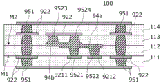
In embodiment 5, the multilayer substrate 90 further includes interlayer connection conductors 9523 and 9524. Fig. 13 is a cross-sectional view of a multilayer substrate 90 according to embodiment 5.
The interlayer connection conductors 9523 and 9524 penetrate the thermoplastic resin layer 113. One end of the interlayer connection conductors 9523 and 9524 is connected to the 2 nd conductor pattern 94. The other ends of the interlayer connection conductors 9523 and 9524 are connected to the 1 st conductor pattern 922. The area of one end of the interlayer connection conductors 9523, 9524 is larger than the area of the other end of the interlayer connection conductors 9523, 9524.
Further, the interlayer connection conductor 9521 and the interlayer connection conductor 9522 are adjacent. In more detail, the interlayer connection conductor 9521 is located closest to the interlayer connection conductor 9522 in a direction orthogonal to the lamination direction. The interlayer connection conductor 9523 and the interlayer connection conductor 9524 are adjacent. In more detail, the interlayer connection conductor 9523 is located closest to the interlayer connection conductor 9524 in a direction orthogonal to the lamination direction.
Such a multilayer substrate 90 is formed by overlapping a conductive pattern formed on one surface of the thermoplastic resin layer 112 and a conductive pattern formed on one main surface of the thermoplastic resin layer 113, thereby forming the 2 nd conductor pattern 94.
According to the multilayer substrate 90, when the interlayer connection conductors 9521 to 9524 are connected to the ground potential, the shielding property is improved due to the presence of the 2 nd conductor pattern 94.
Embodiment 6
In embodiment 6, the multilayer substrate 100 further includes 2 nd conductor patterns 94a and 94b. Fig. 14 is a cross-sectional view of a multilayer substrate 100 according to embodiment 6.
The multilayer substrate 100 is different from the multilayer substrate 90 in that the 2 nd type conductor pattern 94 is separated into the 2 nd type conductor patterns 94a, 94b, and the 2 nd type conductor patterns 94a, 94b are deviated in a direction orthogonal to the lamination direction. The other ends of the interlayer connection conductors 9521 and 9522 are connected to the 2 nd type conductor pattern 94a formed on the other surface of the thermoplastic resin layer 112. One ends of interlayer connection conductors 9521 and 9522 are connected to the 1 st type conductor patterns 9211 and 9212, respectively. The area of the other ends of the interlayer connection conductors 9521, 9522 is larger than the area of one ends of the interlayer connection conductors 9521, 9522.
One end of the interlayer connection conductors 9523 and 9524 is connected to the 2 nd type conductor pattern 94b formed on one surface of the thermoplastic resin layer 112. The other ends of the interlayer connection conductors 9523 and 9524 are connected to the 1 st conductor pattern 922. The area of one end of the interlayer connection conductors 9523, 9524 is larger than the area of the other end of the interlayer connection conductors 9523, 9524.
However, the 2 nd type conductor pattern 94b is deviated from the 2 nd type conductor pattern 94a in a direction orthogonal to the lamination direction. Therefore, a step is formed at the boundary between the 2 nd conductor pattern 94a and the 2 nd conductor pattern 94b. The multilayer substrate 100 described above exhibits the same operational effects as the multilayer substrate 90.
Embodiment 7
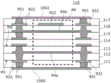
In embodiment 7, a shielding region A0 is formed on the multilayer substrate 110. Fig. 15 is a cross-sectional view of a multilayer substrate 110 according to embodiment 7.
In more detail, the shielding region A0 is located between the 1 st kind of conductor pattern 1000 provided on one surface of the multilayer substrate 110 and the 1 st kind of conductor pattern 1002 provided on the other surface of the multilayer substrate 110. Further, interlayer connection conductors 951 are provided on both sides of the shielding region A0 in a direction orthogonal to the stacking direction. The 1 st type conductor patterns 1000 and 1002 and the interlayer connection conductor 951 are connected to a ground potential. Thereby, the periphery of the shield region A0 is surrounded by the 1 st type conductor patterns 1000 and 1002 connected to the ground potential and the interlayer connection conductor 951.
An electronic circuit which is not affected by noise is provided in the shielding region A0 as described above. Such an electronic circuit is, for example, a high-frequency circuit, an active element, an IC (Integrated Circuit ).
In the multilayer substrate 110, the interlayer connection conductors 951 may be connected to both ends of the 2 nd type conductor pattern 94a from both sides in the stacking direction, or the interlayer connection conductors 951 may be connected to both ends of the 2 nd type conductor pattern 94a from one side or the other side in the stacking direction. Further, the interlayer connection conductors 951 may be connected to both ends of the 2 nd type conductor pattern 94b from both sides in the stacking direction, or the interlayer connection conductors 951 may be connected to both ends of the 2 nd type conductor pattern 94b from one side or the other side in the stacking direction.
The signal conductor layer may be provided in the shield region A0 as described above. By the presence of the 2 nd type conductor pattern 94a between the end portion of the multilayer substrate 110, noise radiation to the outside of the multilayer substrate 110 can be suppressed.
Embodiment 8
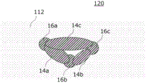
In embodiment 8, the multilayer substrate 120 includes interlayer connection conductors 16a to 16c and 2 nd type conductor patterns 14a to 14c. Fig. 16 is a plan view of the interlayer connection conductors 16a to 16c and the 2 nd type conductor patterns 14a to 14c in the stacking direction.
The interlayer connection conductors 16a to 16c penetrate the thermoplastic resin layer 112 in the lamination direction. The 2 nd type conductor patterns 14a to 14c are formed on the other surface of the thermoplastic resin layer 112. The 2 nd conductive patterns 14a to 14c connect the interlayer connection conductors 16a to 16 c. Specifically, the 2 nd conductor pattern 14a connects the interlayer connection conductor 16a (1 st interlayer connection conductor) and the interlayer connection conductor 16b (2 nd interlayer connection conductor). The 2 nd conductor pattern 14b connects the interlayer connection conductor 16b (2 nd interlayer connection conductor) and the interlayer connection conductor 16c (3 rd interlayer connection conductor). The 2 nd conductor pattern 14c connects the interlayer connection conductor 16c (3 rd interlayer connection conductor) and the interlayer connection conductor 16a (1 st interlayer connection conductor).
In the multilayer substrate 120, the proportion of the 2 nd type conductor patterns 14a to 14c in the multilayer substrate 120 is increased when viewed in the lamination direction. Therefore, when the 2 nd conductor patterns 14a to 14c are connected to the ground potential, the shielding performance of the multilayer substrate 120 is improved.
Further, the 2 nd type conductor pattern 14a and the 2 nd type conductor pattern 14b are connected into one. Thus, when the 2 nd conductor patterns 14a and 14b are connected to the ground potential, the shielding performance of the multilayer substrate 120 is further improved.
Embodiment 9
In embodiment 9, the multilayer substrate 130 includes signal conductors 200a and 200b. Fig. 17 is a cross-sectional view of multilayer substrate 130 according to embodiment 9. Fig. 18 is a plan view of the thermoplastic resin layer 111. Fig. 19 is a plan view of the thermoplastic resin layer 112.
The signal conductors 200a, 200b are formed on the other surface of the thermoplastic resin layer 111. Between the signal conductor layers 200a and 200b, a plurality of interlayer connection conductors 15 are arranged along the signal conductor layers 200a and 200b. This improves the isolation between the signal conductor layers 200a and 200b.
Further, the plurality of interlayer connection conductors 15 are connected by the 2 nd conductor pattern 14 provided in the thermoplastic resin layer 112.
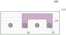
In embodiment 10, two non-adjacent interlayer connection conductors 15 of the multilayer substrate 140 are connected by the 2 nd type conductor pattern 14. Fig. 20 is a plan view of the thermoplastic resin layer 112.
As shown in fig. 20, the interlayer connection conductor 15 which is not connected to the 2 nd type conductor pattern 14 may be located between two interlayer connection conductors 15 connected by the 2 nd type conductor pattern 14.
As described above, the 2 nd conductor pattern can be used for realizing various electric functions.
The 2 nd conductor pattern may be a functional pattern or a pattern for obtaining only electrical connection.
A diffusion layer may be formed between the 1 st conductive pattern and the interlayer connection conductor. The diffusion layer is an alloy region formed by diffusing a metal in the 1 st kind of conductor pattern into the interlayer connection conductor and/or diffusing a metal in the interlayer connection conductor into the 1 st kind of conductor pattern.
The 1 st conductive pattern may include a rust preventive layer. The rust preventive layer contains Ni and W, for example. The rust preventive layer is provided on the surface of a copper foil as an example of a metal foil. In addition, the rust preventive layer existing on the bottom surface of the hole may be removed entirely. In addition, a part of the rust preventive layer existing on the bottom surface of the hole may remain. If the rust preventive layer is removed entirely, the 1 st conductive pattern and the interlayer connection conductor are connected more reliably.
The 2 nd conductor pattern may be arranged between the 1 st signal conductor and the 2 nd signal conductor. Therefore, the 2 nd conductor pattern may be arranged between the 1 st signal conductor and the 2 nd signal conductor in the stacking direction, or may be arranged between the 1 st signal conductor and the 2 nd signal conductor in a direction orthogonal to the stacking direction.
Finally, the above description of the embodiments is illustrative in all respects, rather than restrictive. Modifications and variations can be made as appropriate to those skilled in the art. The scope of the utility model is not shown by the embodiments described above but by the claims. Further, the scope of the present utility model includes modifications from the embodiments within the scope equivalent to the claims.
Description of the reference numerals
10. 40, 50, 60, 70, 80, 90, 100, 110, 120, 130, 140: a multilayer substrate;
12. 13, 622, 721, 722, 822, 6211, 6212, 8211, 8212: a 1 st kind of conductor pattern;
14. 64, 74, 84: a 2 nd conductor pattern;
15. 16, 651, 751, 752, 85, 6521, 6522: an interlayer connection conductor;
21: a hole;
22: a concave portion;
23: a wall portion;
34. 35: a conductive paste;
111-115: a thermoplastic resin layer;
311 to 315: and a resin sheet.
Claims (12)
1. A multilayer substrate comprising a plurality of thermoplastic resin layers including a 1 st thermoplastic resin layer and a 2 nd thermoplastic resin layer, characterized in that,
the multilayer substrate is provided with:
a 1 st kind of conductor pattern formed by a conductor foil on one surface of the 1 st thermoplastic resin layer;
a 2 nd conductive pattern disposed so as to contact the other surface of the 1 st thermoplastic resin layer; and
a 1 st interlayer connection conductor formed on the 1 st thermoplastic resin layer, connected to the 1 st conductor pattern on the 1 st end face, connected to the 2 nd conductor pattern on the 2 nd end face,
the 2 nd thermoplastic resin layer is in contact with the other surface of the 1 st thermoplastic resin layer,
the 2 nd conductor pattern and the 1 st interlayer connection conductor are formed of conductive members of the same material including a resin or conductive members of the same material including a metal having a lower melting point than the conductor foil.
2. The multilayer substrate according to claim 1, wherein,
the area of the 2 nd end face is larger than that of the 1 st end face.
3. The multilayer substrate according to claim 1, wherein,
the side of the 2 nd conductive pattern is in contact with the 1 st thermoplastic resin layer.
4. The multilayer substrate according to claim 3, wherein,
the 1 st thermoplastic resin layer has a concave portion,
the recess is formed along the 2 nd conductor pattern to accommodate the 2 nd conductor pattern.
5. The multilayer substrate according to claim 4, wherein,
the roughness of the bottom surface and the side surface of the recess is greater than the roughness of the portion of the other surface of the 1 st thermoplastic resin layer where the recess is not formed.
6. The multilayer substrate according to any one of claim 1 to 5, wherein,
the 2 nd conductor pattern is a conductor pattern for an inductor.
7. The multilayer substrate according to any one of claim 1 to 5, wherein,
the 2 nd conductor pattern is a conductor pattern for a capacitor.
8. The multilayer substrate according to any one of claim 1 to 5, wherein,
the device further comprises: a 2 nd interlayer connection conductor formed on the 1 st thermoplastic resin layer,
the 2 nd conductor pattern connects the 1 st interlayer connection conductor and the 2 nd interlayer connection conductor, and the 2 nd conductor pattern and the 2 nd interlayer connection conductor are formed of conductive members of the same material.
9. The multilayer substrate according to claim 8, wherein,
the 1 st interlayer connection conductor is adjacent to the 2 nd interlayer connection conductor.
10. The multilayer substrate according to claim 8, wherein,
the device further comprises: a 3 rd interlayer connection conductor formed on the 1 st thermoplastic resin layer,
the 2 nd conductor pattern connects the 1 st interlayer connection conductor, the 2 nd interlayer connection conductor, and the 3 rd interlayer connection conductor.
11. The multilayer substrate according to any one of claim 1 to 5, wherein,
the device further comprises: the 1 st signal conductor and the 2 nd signal conductor are formed by conductor foils,
the 2 nd conductor pattern is arranged between the 1 st signal conductor and the 2 nd signal conductor to constitute a shield conductor.
12. The multilayer substrate according to any one of claim 1 to 5, wherein,
there is no conductor pattern formed of a conductor foil between the other face of the 2 nd conductor pattern and the one face of the 2 nd thermoplastic resin layer.
Applications Claiming Priority (3)
| Application Number | Priority Date | Filing Date | Title |
|---|---|---|---|
| JP2020-096562 | 2020-06-03 | ||
| JP2020096562 | 2020-06-03 | ||
| PCT/JP2021/021109 WO2021246467A1 (en) | 2020-06-03 | 2021-06-03 | Multilayer substrate and method for manufacturing same |
Publications (1)
| Publication Number | Publication Date |
|---|---|
| CN219204859U true CN219204859U (en) | 2023-06-16 |
Family
ID=78831224
Family Applications (1)
| Application Number | Title | Priority Date | Filing Date |
|---|---|---|---|
| CN202190000490.9U Active CN219204859U (en) | 2020-06-03 | 2021-06-03 | Multilayer substrate |
Country Status (4)
| Country | Link |
|---|---|
| US (1) | US20230053211A1 (en) |
| JP (1) | JP7338793B2 (en) |
| CN (1) | CN219204859U (en) |
| WO (1) | WO2021246467A1 (en) |
Family Cites Families (5)
| Publication number | Priority date | Publication date | Assignee | Title |
|---|---|---|---|---|
| JP4181778B2 (en) | 2002-02-05 | 2008-11-19 | ソニー株式会社 | Wiring board manufacturing method |
| JP2005251949A (en) * | 2004-03-03 | 2005-09-15 | Sony Corp | Wiring board and method for manufacturing the same |
| EP3570649A1 (en) | 2009-11-10 | 2019-11-20 | Murata Manufacturing Co., Ltd. | Multilayer board and manufacturing method thereof |
| CN103430639B (en) | 2011-03-17 | 2016-09-28 | 株式会社村田制作所 | Resin multilayer substrate |
| JP6641726B2 (en) * | 2015-05-13 | 2020-02-05 | 株式会社村田製作所 | Method for manufacturing resin multilayer substrate |
-
2021
- 2021-06-03 JP JP2022528882A patent/JP7338793B2/en active Active
- 2021-06-03 WO PCT/JP2021/021109 patent/WO2021246467A1/en active Application Filing
- 2021-06-03 CN CN202190000490.9U patent/CN219204859U/en active Active
-
2022
- 2022-11-02 US US17/979,032 patent/US20230053211A1/en active Pending
Also Published As
| Publication number | Publication date |
|---|---|
| JPWO2021246467A1 (en) | 2021-12-09 |
| WO2021246467A1 (en) | 2021-12-09 |
| JP7338793B2 (en) | 2023-09-05 |
| US20230053211A1 (en) | 2023-02-16 |
Similar Documents
| Publication | Publication Date | Title |
|---|---|---|
| JP6065119B2 (en) | Multilayer board | |
| CN110402615B (en) | Printed circuit board for high-frequency transmission | |
| US11956903B2 (en) | Transmission line, method of manufacturing transmission line, and electronic apparatus | |
| JP7001101B2 (en) | Interposers and electronic devices | |
| CN213124101U (en) | Multilayer substrate and mounting structure for multilayer substrate | |
| US9444126B2 (en) | High-frequency signal line | |
| JP5672091B2 (en) | Multilayer board | |
| JP2000151041A (en) | Printed wiring board | |
| US20210065975A1 (en) | Method for producing multilayer coil component and multilayer coil component | |
| CN219204859U (en) | Multilayer substrate | |
| CN210899888U (en) | Multilayer substrate and electronic device | |
| US11856693B2 (en) | Resin multilayer substrate and method for manufacturing resin multilayer substrate | |
| CN219421172U (en) | Circuit board and connection structure for circuit board | |
| US11246214B2 (en) | Resin multilayer board | |
| JP6741183B2 (en) | Multilayer substrate and electric element | |
| CN217405406U (en) | Multilayer substrate | |
| JP2022002260A (en) | Surface-mounted passive component | |
| US20230225092A1 (en) | Electronic component module and method of manufacturing electronic component module | |
| US20230284381A1 (en) | Multilayer substrate and method for manufacturing multilayer substrate | |
| CN218587412U (en) | Multilayer substrate | |
| JP7095739B2 (en) | Manufacturing method of electric element | |
| US20230239996A1 (en) | Circuit board and method of manufacturing circuit board | |
| CN111149177B (en) | Inductor and method for manufacturing the same | |
| CN211828497U (en) | Resin multilayer substrate and electronic device | |
| JPWO2022113779A5 (en) |
Legal Events
| Date | Code | Title | Description |
|---|---|---|---|
| GR01 | Patent grant | ||
| GR01 | Patent grant |