EP3568720B1 - Film composite réfléchissant les infrarouges et conducteur électrique et son procédé de fabrication - Google Patents
Film composite réfléchissant les infrarouges et conducteur électrique et son procédé de fabrication Download PDFInfo
- Publication number
- EP3568720B1 EP3568720B1 EP18700145.8A EP18700145A EP3568720B1 EP 3568720 B1 EP3568720 B1 EP 3568720B1 EP 18700145 A EP18700145 A EP 18700145A EP 3568720 B1 EP3568720 B1 EP 3568720B1
- Authority
- EP
- European Patent Office
- Prior art keywords
- composite film
- layer
- infrared reflective
- substrate
- inferior
- Prior art date
- Legal status (The legal status is an assumption and is not a legal conclusion. Google has not performed a legal analysis and makes no representation as to the accuracy of the status listed.)
- Active
Links
- 239000002131 composite material Substances 0.000 title claims description 88
- 238000004519 manufacturing process Methods 0.000 title claims description 5
- 229910052751 metal Inorganic materials 0.000 claims description 61
- 239000002184 metal Substances 0.000 claims description 61
- 239000000758 substrate Substances 0.000 claims description 46
- 239000002070 nanowire Substances 0.000 claims description 26
- 239000002245 particle Substances 0.000 claims description 21
- 238000009736 wetting Methods 0.000 claims description 17
- 238000000151 deposition Methods 0.000 claims description 12
- BQCADISMDOOEFD-UHFFFAOYSA-N Silver Chemical compound [Ag] BQCADISMDOOEFD-UHFFFAOYSA-N 0.000 claims description 10
- 238000000034 method Methods 0.000 claims description 9
- 239000004332 silver Substances 0.000 claims description 8
- 229910044991 metal oxide Inorganic materials 0.000 claims description 7
- 150000004706 metal oxides Chemical class 0.000 claims description 7
- 229910052709 silver Inorganic materials 0.000 claims description 7
- 238000000231 atomic layer deposition Methods 0.000 claims description 4
- 230000001788 irregular Effects 0.000 claims description 4
- 238000009718 spray deposition Methods 0.000 claims description 3
- 239000010410 layer Substances 0.000 description 136
- 230000003287 optical effect Effects 0.000 description 14
- 230000005540 biological transmission Effects 0.000 description 7
- 239000011521 glass Substances 0.000 description 7
- 238000000576 coating method Methods 0.000 description 6
- 230000000007 visual effect Effects 0.000 description 6
- 238000010438 heat treatment Methods 0.000 description 5
- 239000002105 nanoparticle Substances 0.000 description 4
- 230000008021 deposition Effects 0.000 description 3
- 230000005855 radiation Effects 0.000 description 3
- 239000002042 Silver nanowire Substances 0.000 description 2
- 230000004888 barrier function Effects 0.000 description 2
- 238000005516 engineering process Methods 0.000 description 2
- 239000002346 layers by function Substances 0.000 description 2
- 230000008569 process Effects 0.000 description 2
- 238000010257 thawing Methods 0.000 description 2
- 229910001316 Ag alloy Inorganic materials 0.000 description 1
- FOIXSVOLVBLSDH-UHFFFAOYSA-N Silver ion Chemical compound [Ag+] FOIXSVOLVBLSDH-UHFFFAOYSA-N 0.000 description 1
- UCKMPCXJQFINFW-UHFFFAOYSA-N Sulphide Chemical compound [S-2] UCKMPCXJQFINFW-UHFFFAOYSA-N 0.000 description 1
- 230000004075 alteration Effects 0.000 description 1
- 238000005452 bending Methods 0.000 description 1
- 230000008859 change Effects 0.000 description 1
- 239000011248 coating agent Substances 0.000 description 1
- 239000004020 conductor Substances 0.000 description 1
- 239000005340 laminated glass Substances 0.000 description 1
- 238000001459 lithography Methods 0.000 description 1
- 239000000463 material Substances 0.000 description 1
- 229910001092 metal group alloy Inorganic materials 0.000 description 1
- 239000002086 nanomaterial Substances 0.000 description 1
- 230000007935 neutral effect Effects 0.000 description 1
- 150000004767 nitrides Chemical class 0.000 description 1
- 229920002037 poly(vinyl butyral) polymer Polymers 0.000 description 1
- 229920006254 polymer film Polymers 0.000 description 1
- 229920000307 polymer substrate Polymers 0.000 description 1
- 230000001681 protective effect Effects 0.000 description 1
- 238000001228 spectrum Methods 0.000 description 1
- 238000004544 sputter deposition Methods 0.000 description 1
- 238000007669 thermal treatment Methods 0.000 description 1
- XOLBLPGZBRYERU-UHFFFAOYSA-N tin dioxide Chemical compound O=[Sn]=O XOLBLPGZBRYERU-UHFFFAOYSA-N 0.000 description 1
- 229910001887 tin oxide Inorganic materials 0.000 description 1
- 239000012780 transparent material Substances 0.000 description 1
Images


Classifications
-
- G—PHYSICS
- G02—OPTICS
- G02B—OPTICAL ELEMENTS, SYSTEMS OR APPARATUS
- G02B5/00—Optical elements other than lenses
- G02B5/08—Mirrors
- G02B5/0816—Multilayer mirrors, i.e. having two or more reflecting layers
- G02B5/085—Multilayer mirrors, i.e. having two or more reflecting layers at least one of the reflecting layers comprising metal
- G02B5/0875—Multilayer mirrors, i.e. having two or more reflecting layers at least one of the reflecting layers comprising metal the reflecting layers comprising two or more metallic layers
-
- G—PHYSICS
- G02—OPTICS
- G02B—OPTICAL ELEMENTS, SYSTEMS OR APPARATUS
- G02B5/00—Optical elements other than lenses
- G02B5/20—Filters
- G02B5/208—Filters for use with infrared or ultraviolet radiation, e.g. for separating visible light from infrared and/or ultraviolet radiation
-
- C—CHEMISTRY; METALLURGY
- C23—COATING METALLIC MATERIAL; COATING MATERIAL WITH METALLIC MATERIAL; CHEMICAL SURFACE TREATMENT; DIFFUSION TREATMENT OF METALLIC MATERIAL; COATING BY VACUUM EVAPORATION, BY SPUTTERING, BY ION IMPLANTATION OR BY CHEMICAL VAPOUR DEPOSITION, IN GENERAL; INHIBITING CORROSION OF METALLIC MATERIAL OR INCRUSTATION IN GENERAL
- C23C—COATING METALLIC MATERIAL; COATING MATERIAL WITH METALLIC MATERIAL; SURFACE TREATMENT OF METALLIC MATERIAL BY DIFFUSION INTO THE SURFACE, BY CHEMICAL CONVERSION OR SUBSTITUTION; COATING BY VACUUM EVAPORATION, BY SPUTTERING, BY ION IMPLANTATION OR BY CHEMICAL VAPOUR DEPOSITION, IN GENERAL
- C23C16/00—Chemical coating by decomposition of gaseous compounds, without leaving reaction products of surface material in the coating, i.e. chemical vapour deposition [CVD] processes
- C23C16/22—Chemical coating by decomposition of gaseous compounds, without leaving reaction products of surface material in the coating, i.e. chemical vapour deposition [CVD] processes characterised by the deposition of inorganic material, other than metallic material
- C23C16/30—Deposition of compounds, mixtures or solid solutions, e.g. borides, carbides, nitrides
- C23C16/40—Oxides
- C23C16/407—Oxides of zinc, germanium, cadmium, indium, tin, thallium or bismuth
-
- C—CHEMISTRY; METALLURGY
- C23—COATING METALLIC MATERIAL; COATING MATERIAL WITH METALLIC MATERIAL; CHEMICAL SURFACE TREATMENT; DIFFUSION TREATMENT OF METALLIC MATERIAL; COATING BY VACUUM EVAPORATION, BY SPUTTERING, BY ION IMPLANTATION OR BY CHEMICAL VAPOUR DEPOSITION, IN GENERAL; INHIBITING CORROSION OF METALLIC MATERIAL OR INCRUSTATION IN GENERAL
- C23C—COATING METALLIC MATERIAL; COATING MATERIAL WITH METALLIC MATERIAL; SURFACE TREATMENT OF METALLIC MATERIAL BY DIFFUSION INTO THE SURFACE, BY CHEMICAL CONVERSION OR SUBSTITUTION; COATING BY VACUUM EVAPORATION, BY SPUTTERING, BY ION IMPLANTATION OR BY CHEMICAL VAPOUR DEPOSITION, IN GENERAL
- C23C16/00—Chemical coating by decomposition of gaseous compounds, without leaving reaction products of surface material in the coating, i.e. chemical vapour deposition [CVD] processes
- C23C16/44—Chemical coating by decomposition of gaseous compounds, without leaving reaction products of surface material in the coating, i.e. chemical vapour deposition [CVD] processes characterised by the method of coating
- C23C16/455—Chemical coating by decomposition of gaseous compounds, without leaving reaction products of surface material in the coating, i.e. chemical vapour deposition [CVD] processes characterised by the method of coating characterised by the method used for introducing gases into reaction chamber or for modifying gas flows in reaction chamber
- C23C16/45523—Pulsed gas flow or change of composition over time
- C23C16/45525—Atomic layer deposition [ALD]
-
- G—PHYSICS
- G02—OPTICS
- G02B—OPTICAL ELEMENTS, SYSTEMS OR APPARATUS
- G02B5/00—Optical elements other than lenses
- G02B5/20—Filters
- G02B5/204—Filters in which spectral selection is performed by means of a conductive grid or array, e.g. frequency selective surfaces
-
- G—PHYSICS
- G02—OPTICS
- G02B—OPTICAL ELEMENTS, SYSTEMS OR APPARATUS
- G02B5/00—Optical elements other than lenses
- G02B5/20—Filters
- G02B5/26—Reflecting filters
-
- G—PHYSICS
- G02—OPTICS
- G02B—OPTICAL ELEMENTS, SYSTEMS OR APPARATUS
- G02B5/00—Optical elements other than lenses
- G02B5/20—Filters
- G02B5/28—Interference filters
- G02B5/281—Interference filters designed for the infrared light
- G02B5/282—Interference filters designed for the infrared light reflecting for infrared and transparent for visible light, e.g. heat reflectors, laser protection
Definitions
- the invention is directed to an optically transparent composite film combining heat reflective properties and electrical conductivity to coat on a substrate, preferably on an optically transparent substrate.
- Infrared reflective and electrically conductive coatings on glass substrate are used to reduce heat transfer through the substrate and provide resistive heating for defogging and/or defrosting. Said coatings are used in particular in the building and automotive glazing domains.
- Prior art patent document published US 2011/0268941 A1 discloses a process for manufacturing a glazing unit with 3 or 4 functional layers made of silver that can act on solar radiation and/or infrared radiation, as well as resistive heater.
- One objective is to provide a multilayer that has a low surface resistivity, a high light transmission and a relatively neutral colour, and that can undergo a heat treatment above 600°C without significant change of the properties.
- the glazing unit comprises a laminated structure.
- the glazing unit comprises a transparent glass substrate coated with a composite film comprising an alteration of one functional layer based on silver or metal alloy containing silver and positioned between two antireflection coatings. The coatings are deposited on the substrate by the vacuum technique.
- the composite film can be used to form heated glazing unit.
- the limitation of the structure is the absence of versatility on the visual aspect, particularly on the reflected colour. Moreover, the requirement to be able to undergo a heat treatment above 600°C makes the structure complex and difficult to modify as a function of new requirements from
- Prior art patent document published US 2015/0185382 A1 discloses a transparent infrared reflective and low emissivity composite film.
- the composite film is configured to be coated on a transparent substrate and comprises at least one silver based layer which provides infrared reflective (IRR) properties, at least one metal based layer and at least one metal oxide based layers and an atomic layer deposited (ALD) metal oxide layer on the top of the composite film.
- the composite film does not provide any electrical conductivity to said composite and does not reach good optical properties.
- Prior art patent document published US 2015/0183301 A1 discloses an optically transparent and infrared reflecting (IRR) composite film.
- the composite film is configured to be coated on a glass substrate.
- the film comprises at least one metal based layer, at least one silver based layer used to reflect infrared radiation and at least one metal oxide based layer.
- the composite film does not provide any electrical conductivity to said composite and does not reach good optical properties.
- Prior art patent document published US 2017/0145737 A1 discloses an optically transparent and infrared reflecting (IRR) composite film.
- the composite film combines in a same layer a metal layer of connected metal nanowires and an infrared reflective layer.
- Prior art patent document published EP 2 374 559 A2 discloses an optically transparent and infrared reflecting (IRR) composite film.
- the composite film comprises at least layer of nanoparticles which may be in the form of disks and which may include a transparent metal oxide layer on the particles.
- the cited prior art disclosed composite films that show a limited figure of merit in terms of low heat transmission, high optical transmission, low electrical resistance and well defined colour.
- the cited prior art discloses composite films that are deposited by vacuum technology, mainly sputtering, on flat substrates prior to high temperature treatment.
- the disclosed composite films are complex and contain a lot of layers in order to be able to stand additional processing steps, including high temperature heating and in order to reach good infrared reflective and optical properties and/or electrical conductive properties.
- the process described in this prior art allows only very low versatility for changing the visual parameters of the resulting films.
- the invention has for technical problem to provide a solution which overcomes at least one drawback of the cited prior art. More particularly, the invention has for technical problem to provide an optically transparent composite film, to coat on a substrate, comprising a simple structure and which reaches improved optical transmission, infrared reflection and electrical conductive properties, while allowing larger flexibility in terms of visual aspect, in particular reflected colour.
- the invention has also for technical problem to provide a method for the realization of a product coated with a composite film combining heat reflective, electrical conductivity and good optical properties.
- the invention is directed to an infrared reflective and electrically conductive composite film to coat or to be applied or to deposit on a substrate, said composite film comprising at least one infrared reflective layer; remarkable in that said composite film further comprises at least one metal layer of connected metal nanowires, each of said at least one infrared reflective layer and at least one metal layer being conformably covered by an optically transparent conductive layer.
- the at least one infrared reflective layer has a surface coverage rate of at least 30%.
- the at least one infrared reflective layer is a layer of silver nanostructured particles with irregular shape or disk shape and/or the metal nanowires are silver nanowires.
- the nanostructured particles of the at least one infrared reflective layer are separated from each other with a gap inferior to 1 ⁇ m, preferably inferior to 100 nm.
- the nanostructured particles of the at least one infrared reflective layer have different aspect ratio.
- the nanostructured particles of the at least one infrared reflective layer have an average diameter comprised between 1 nm and 10 ⁇ m, preferably between 10 nm and 1 ⁇ m.
- the at least one infrared reflective layer has a thickness comprised between 1 nm and 30 nm.
- the connected metal nanowires of the metal layer or each of the metal layer have a surface coverage rate inferior to 20%, preferably inferior to 10%.
- the connected metal nanowires have a length superior to 100 nm, preferably superior to 10 ⁇ m, a width inferior to 10 ⁇ m, preferably inferior to 100 nm and/or a thickness inferior to 300 nm, preferably inferior to 100 nm wherein the width and the thickness of the nanowires are respectively related to a plane parallel to an average plane of the substrate and to a plane transversal to an average plane of the substrate.
- each transparent conductive layer is an optically transparent conductive metal oxide.
- each transparent conductive layer has a thickness comprised between 10 and 1000 nm.
- the composite film further comprises at least one wetting layer, said wetting layer or each wetting layer being coated by an infrared reflective layer or by a metal layer.
- the wetting layer or each wetting layer has a thickness inferior to 10 nm.
- the composite film comprised between 1 and 5 infrared reflective layers and between 1 and 3 metal layers.
- the invention is also directed to a method for producing a product comprising the steps of providing a substrate, depositing a composite film on said substrate, remarkable in that the composite film of step of depositing a composite film comprises at least one infrared reflective layer and at least one metal layer of connected metal nanowires, each of said at least one infrared reflective layer and at least one metal layer being conformably covered by an optically transparent conductive layer, said composite film being in accordance with the invention.
- the method further comprises a step of depositing electrical contacts on said substrate.
- said electrical contacts are deposited on the substrate before the composite film or before at least one infrared reflective layer or at least one metal layer.
- the step of depositing the composite film is performed by atomic layer deposition and spray deposition.
- the invention is particularly interesting in that the composite film comprises at least one infrared reflective layer preferably of nanostructures particles and at least one metal layer, each of said layers being conformably covered by a transparent conducting layer.
- the configuration of the composite film according to the invention provides good infrared reflection and electrical conductive properties to said composite film while keeping a good optical transparency of the composite film and thus the optical transparency of the substrate.
- the invention provides a higher flexibility of the resulting visual aspect, as compared to the prior art, due to the partial decoupling of the infrared reflective layers and the electrical conductive layers, while keeping a high level of performances due to the synergistical electrical conduction provided by the transparent conductive layers.
- the number of layers can be reduced compared to composite film of the prior art with the same level of performances.
- optical transparent is used to mean that a material or a device transmits at least 40%, preferably at least 70%, more preferably at least 90%, of the incident visible light.
- Figure 1 illustrates a product 2 comprising a composite film 4.
- Figure 2, figure 3 and figure 4 respectively represent a cross section of the product 2 of figure 1 according to different embodiments.
- the products of figures 2, 3 and 4 are respectively numbered 2.1, 2.2 and 2.3.
- the product 2 is preferably optically transparent and comprises a substrate 6 and the composite film 4 coated on said substrate.
- the substrate 6 is optically transparent and is made of glass, PET or any optically transparent material.
- the substrate 6 can be for example a windshield or a window.
- the composite film 4 is coated on one face of the substrate but can be coated on more faces of said substrate.
- the composite film 4 comprises at least one infrared reflective layer 8 and at least one metal layer 10 of connected metal nanowires.
- Each of the at least one infrared reflective layer 8 and the at least one metal layer 10 is conformably coated by an optically transparent conductive layer 12.
- the term "conformably” is used to mean that the transparent conductive layers cover/fit closely to the at least one infrared reflective layer and the at least one metal layer by adapting to the shape of said at least one infrared reflective layer and said at least one metal layer.
- Figure 1 only shows one infrared reflective layer 8 and one metal layer 10.
- the composite film 4 comprises between 1 and 5 infrared reflective layers 8 and between 1 and 3 metal layers 10.
- the at least one infrared reflective layer 8 has a surface coverage rate of at least 30%.
- the at least one infrared reflective layer 8 is advantageously a layer of nanostructured particles, as represented in figures 1, 2 and 3 .
- the nanostructured particles are advantageously flat silver nanoparticles with an irregular shape or with a disk shape.
- the nanoparticles are nanodisks.
- the term "nanodisk” is well-known by a skilled-man.
- the term “irregular” is used to describe nanoparticles whose contour does not form a perfect circle or disk.
- the nanostructured particles have an average diameter comprised between 1 nm and 10 ⁇ m, preferably between 10 nm and 1 ⁇ m.
- the nanostructured particles of the at least one infrared reflective layer 8 are separated from each other with a gap inferior to 10 ⁇ m, preferably inferior to 100 nm.
- the nanostructured particles of the at least one infrared reflective layer 8 have different aspect ratio and different surface coverage. In each of the at least one infrared reflective layer 8, the nanostructured particles cover different regions of said layer for larger reflection spectrum.
- the nanostructured particles are advantageously atomic layer deposited nanostructured particles, but not limited to it.
- the connected metal nanowires of the at least one metal layer 10 have a surface coverage rate inferior to 20%, preferably inferior to 10%.
- the connected metal nanowires of the at least one metal layer 10 are preferably connected silver nanowires.
- the connected nanowires can form a disordered network of nanowires as represented in figure 1 or can be in the form of a metal nanogrid (not represented).
- the connected metal nanowires have a width inferior to 10 ⁇ m, preferably inferior to 100 nm and a thickness inferior to 300 nm, preferably inferior to 100 nm.
- the width and the thickness of the nanowires are respectively related to a plane parallel to an average plane of the substrate and to a plane transversal to an average plane of the substrate.
- the connected metal nanowires have a length superior to 100 nm, preferably superior to 10 ⁇ m.
- the connected metal nanowires form a network with a length between connexions superior to 100 nm, preferably superior to 1 ⁇ m. In case of a disordered network of nanowires, the length between the connexions is inferior to the length of the nanowires.
- the connected nanowires can be deposited by spray-deposition.
- the metal grid can be a mesh realised by lithography or by dewetting of a metal layer. The use of connected metal nanowires allows to provide an electrical conductive layer in the composite film 4 while keeping a good optical transparency of said layer.
- Each transparent conductive layer 12 conformably covers the nanostructured particles of the at least one infrared reflective layer 8 and the connected metal nanowires of the at least one metal layer 10, in order to form a flattened surface.
- the transparent conductive layers 12 are advantageously deposited by Atomic Layer Deposition (ALD) but not limited to it.
- ALD Atomic Layer Deposition
- Each transparent conductive layer 12 is a layer of an optically transparent conductive material, preferentially transparent conductive metal oxide such as but not limited to Al-doped ZnO layer or tin oxide.
- Each transparent conductive layer 12 has a thickness comprised between 10 and 1 ⁇ m. Each transparent conductive layer 12 have different thickness, or have the same thickness.
- the combination of at least one infrared layer and at least one metal layer of connected metal nanowires, with conformal transparent conductive layers provides a solution to obtain optimum infrared reflective and electrical resistance properties of the composite film 4, while keeping good optical properties of the composite film in terms of optical transmission and visual aspect.
- infrared reflective layers 8 with nanostructured particles of different aspect ratios allows to improve the surface coverage of the nanostructured particles in the composite film, thus improving the infrared reflective properties of the composite film, while maintaining a good optical transparency of said composite film.
- the infrared reflective layer 8 is under the metal layer 10, said configuration does not limit the invention. Indeed, the metal layer 10 can also be above the infrared reflective layer 8, as represented in figure 3 .
- the terms "above” and “under” are related to the substrate. In case of more than one metal layer 10 and more than one infrared reflective layer 8, many configurations of the composite film 4 are possible.
- One or several infrared reflective layers 8 can be made of disconnected nanoparticles as represented in figures 1, 2 and 3 , or of a continuous metal film corresponding to a surface coverage of 100%, as represented in figure 4 .
- the composite film 4 can also comprise at least one wetting layer (not represented).
- the wetting layer or each wetting layer is coated by an infrared reflective layer 8 or a metal layer 10.
- the at least one wetting layer promotes deposition of an infrared reflective layer 8 and/or of a metal layer 10.
- the wetting layer can be made of metal or oxide or nitride or sulfide layer or a combination.
- the at least one wetting layer is made of silver.
- the at least one wetting layer has a thickness inferior to 10 nm.
- the composite film 4 can also comprise supplementary layers such as supplementary transparent conductive layers 12, protective insulating layers, anti-reflecting layers or index matching layers, gas barrier layers and/or haze reducing layers (not represented).
- FIG. 5 illustrates an example of a product coated with the composite film according to the invention comprising optional additional layers.
- the product 102 is a full optically transparent product.
- the product 102 comprised a substrate 106 which is coated with a composite film 104.
- the composite film 104 comprises two infrared reflective layers 108 and one metal layer 110, each of said layers 108 and 110 being conformably coated with a transparent conductive layer 112.
- the composite film 4 can also comprise others transparent conductive layers 112. More particularly, a transparent conductive layer 112 can be coated on the substrate 106 before deposition of the at least one infrared reflective layers 108 or the at least one metal layer 110.
- the composite film 104 can also comprise optical or barrier layers 114 and a protection layer 116 on the top of the composite film 104, at the opposite side of the substrate 106.
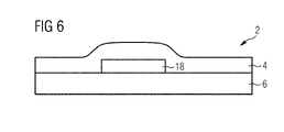
- the product 2 coated with a composite film 4 according to the invention can also comprise electric contacts 18, as illustrated in Figure 6 .
- the electrical contacts 18 are deposited on the substrate 6 before the deposition of the composite film 4 on the substrate, or at least before one of the infrared reflective layer or one metal layer.
- the composite film or at least part of the composite film is deposited after the bending of the substrate.
- the composite film being mostly deposited by atomic layer deposition, allows to have a direct electrical connection between the electrical contacts and said composite film.
- the combination of electrical contacts with the composite film provide defogging and defrosting properties to the product.
- the manufacturing described here does not preclude post thermal treatment at a moderate temperature below 300°C.
- the product comprising a glass substrate coated with the composite film according to the invention can also comprise a polymer film such as a polyvinyl butyral film and a counter substrate glass, in order to form a laminated glass.
- a polymer film such as a polyvinyl butyral film and a counter substrate glass
- the composite film according to the invention can be used to produce low-emissivity windows, glazing in vehicle such as cars, planes or trains, glass for displays and/or transparent polymer substrate (e.g. helmet's eyeshade), all of them can be flat or bended.
- vehicle such as cars, planes or trains
- transparent polymer substrate e.g. helmet's eyeshade
Landscapes
- Physics & Mathematics (AREA)
- Chemical & Material Sciences (AREA)
- Optics & Photonics (AREA)
- General Physics & Mathematics (AREA)
- Toxicology (AREA)
- Health & Medical Sciences (AREA)
- Materials Engineering (AREA)
- Organic Chemistry (AREA)
- Metallurgy (AREA)
- Mechanical Engineering (AREA)
- Engineering & Computer Science (AREA)
- Chemical Kinetics & Catalysis (AREA)
- General Chemical & Material Sciences (AREA)
- Spectroscopy & Molecular Physics (AREA)
- Inorganic Chemistry (AREA)
- Laminated Bodies (AREA)
- Optical Elements Other Than Lenses (AREA)
- Optical Filters (AREA)
- Non-Insulated Conductors (AREA)
Claims (15)
- Film composite (4) réfléchissant l'infrarouge et électriquement conducteur, pour le revêtement d'un substrat (6), ledit film composite (4) comprenant :au moins une couche métallique (10) de nanofils métalliques connectés recouverte de manière conforme par une couche conductrice optiquement transparente (12) qui s'ajuste étroitement et s'adapte à la forme de la au moins une couche métallique (10) de manière à former une surface aplatie ;au moins une couche réfléchissant l'infrarouge (8) étant une couche de particules nanostructurées d'argent de forme irrégulière ou en forme de disque recouverte de manière conforme par une autre couche conductrice optiquement transparente (12) qui s'ajuste étroitement et s'adapte à la forme de la au moins une couche réfléchissant l'infrarouge (8) de manière à former une surface aplatie.
- Film composite (4) selon la revendication 1, caractérisé en ce que la au moins une couche réfléchissant l'infrarouge (8) a un taux de couverture de surface d'au moins 30%.
- Film composite (4) selon l'une des revendications 1 et 2, caractérisé en ce que les particules nanostructurées de la au moins une couche réfléchissant l'infrarouge (8) sont séparées les unes des autres par un espace inférieur à 1 µm, de préférence inférieur à 100 nm.
- Film composite (4) selon l'une quelconque des revendications 1 à 3, caractérisé en ce que les particules nanostructurées de la au moins une couche réfléchissant l'infrarouge (8) ont un rapport d'aspect différent.
- Film composite (4) selon l'une quelconque des revendications 1 à 4, caractérisé en ce que les particules nanostructurées en forme de disque de la au moins une couche réfléchissant l'infrarouge (8) ont un diamètre moyen compris entre 1 nm et 10 µm, de préférence entre 10 nm et 1 µm.
- Film composite (4) selon l'une quelconque des revendications 1 à 5, caractérisé en ce que la au moins une couche réfléchissant l'infrarouge (8) a une épaisseur comprise entre 1 nm et 30 nm.
- Film composite (4) selon l'une quelconque des revendications 1 à 6, caractérisé en ce que les nanofils métalliques connectés de la couche métallique (10) ou de chacune des couches métalliques (10) ont un taux de couverture de surface inférieur à 20%, de préférence inférieur à 10%.
- Film composite (4) selon l'une quelconque des revendications 1 à 7, caractérisé en ce que les nanofils métalliques connectés ont une longueur supérieure à 100 nm, de préférence supérieure à 10 µm, une largeur inférieure à 10 µm, de préférence inférieure à 100 nm et/ou une épaisseur inférieure à 300 nm, de préférence inférieure à 100 nm, la largeur et l'épaisseur des nanofils étant respectivement liées à un plan parallèle à un plan moyen du substrat et à un plan transversal à un plan moyen du substrat (6).
- Film composite (4) selon l'une quelconque des revendications 1 à 8, caractérisé en ce que chaque couche conductrice transparente (12) est un oxyde métallique conducteur optiquement transparent et/ou chaque couche conductrice transparente (12) a une épaisseur comprise entre 10 et 1000 nm.
- Film composite (4) selon l'une quelconque des revendications 1 à 9, caractérisé en ce que ledit film composite (4) comprend en outre au moins une couche de mouillage, ladite couche de mouillage ou chaque couche de mouillage étant revêtue d'une couche réfléchissant l'infrarouge (8) ou d'une couche métallique (10).
- Film composite (4) selon la revendication 10, caractérisé en ce que la couche de mouillage ou chaque couche de mouillage a une épaisseur inférieure à 10 nm.
- Film composite (4) selon l'une quelconque des revendications 1 à 11, caractérisé en ce que ledit film composite (4) comprend entre 1 et 5 couches réfléchissant l'infrarouge (8) et entre 1 et 3 couches métalliques (10).
- Procédé de fabrication d'un produit (2) comprenant les étapes consistant à :- fournir un substrat (6)- déposer un film composite (4) sur ledit substrat (6) ;dans lequel ledit film composite (4) est conforme à l'une quelconque des revendications 1 à 12.
- Procédé selon la revendication 13, caractérisé en ce que ledit procédé comprend en outre une étape consistant à déposer des contacts électriques (18) sur ledit substrat (6).
- Procédé selon la revendication 14, caractérisé en ce que, lors de l'étape de dépôt de contacts électriques sur ledit substrat, lesdits contacts électriques sont déposés sur le substrat (6) avant le film composite (4) ou avant au moins une couche réfléchissant l'infrarouge (8) ou au moins une couche métallique (10) et/ou l'étape de dépôt du film composite est réalisée par dépôt de couche atomique et dépôt par pulvérisation.
Applications Claiming Priority (2)
| Application Number | Priority Date | Filing Date | Title |
|---|---|---|---|
| LU100018A LU100018B1 (en) | 2017-01-11 | 2017-01-11 | Infrared reflective and electrical conductive composite film and manufacturing method thereof |
| PCT/EP2018/050479 WO2018130530A1 (fr) | 2017-01-11 | 2018-01-09 | Film composite réfléchissant les infrarouges et conducteur électrique et son procédé de fabrication |
Publications (2)
| Publication Number | Publication Date |
|---|---|
| EP3568720A1 EP3568720A1 (fr) | 2019-11-20 |
| EP3568720B1 true EP3568720B1 (fr) | 2022-09-28 |
Family
ID=58699208
Family Applications (1)
| Application Number | Title | Priority Date | Filing Date |
|---|---|---|---|
| EP18700145.8A Active EP3568720B1 (fr) | 2017-01-11 | 2018-01-09 | Film composite réfléchissant les infrarouges et conducteur électrique et son procédé de fabrication |
Country Status (8)
| Country | Link |
|---|---|
| US (1) | US11391872B2 (fr) |
| EP (1) | EP3568720B1 (fr) |
| JP (1) | JP7153355B2 (fr) |
| ES (1) | ES2932852T3 (fr) |
| HU (1) | HUE060171T2 (fr) |
| LU (1) | LU100018B1 (fr) |
| PL (1) | PL3568720T3 (fr) |
| WO (1) | WO2018130530A1 (fr) |
Families Citing this family (3)
| Publication number | Priority date | Publication date | Assignee | Title |
|---|---|---|---|---|
| CN115574485A (zh) * | 2019-10-31 | 2023-01-06 | 高丽大学校产学协力团 | 辐射冷却元件及其制作方法 |
| DE102020006108A1 (de) * | 2020-10-06 | 2022-04-07 | Giesecke+Devrient Currency Technology Gmbh | Transparente, leitfähige Folie und Verwendung derselben |
| DE102022117520A1 (de) * | 2022-07-13 | 2024-01-18 | HeiQ RAS AG | Verbundwerkstoff |
Family Cites Families (24)
| Publication number | Priority date | Publication date | Assignee | Title |
|---|---|---|---|---|
| FR2701475B1 (fr) * | 1993-02-11 | 1995-03-31 | Saint Gobain Vitrage Int | Substrats en verre revêtus d'un empilement de couches minces, application à des vitrages à propriétés de réflexion dans l'infra-rouge et/ou à propriétés dans le domaine du rayonnement solaire. |
| JP2010513175A (ja) * | 2006-06-30 | 2010-04-30 | カーディナル・シージー・カンパニー | カーボンナノチューブグレージング技術 |
| FR2936510B1 (fr) | 2008-09-30 | 2019-08-30 | Saint-Gobain Glass France | Substrat muni d'un empilement a proprietes thermiques, en particulier pour realiser un vitrage chauffant. |
| JP5636208B2 (ja) * | 2010-04-07 | 2014-12-03 | 富士フイルム株式会社 | 熱線遮蔽用金属平板状粒子含有組成物 |
| JP2012184140A (ja) * | 2011-03-07 | 2012-09-27 | Nippon Electric Glass Co Ltd | 熱線反射ガラス板 |
| JP5798804B2 (ja) * | 2011-06-03 | 2015-10-21 | 株式会社ブリヂストン | 熱線遮蔽フィルム、これを用いた熱線遮蔽ウィンドウ |
| WO2013035802A1 (fr) * | 2011-09-06 | 2013-03-14 | 富士フイルム株式会社 | Matière de protection vis-à-vis du rayonnement thermique |
| JP2013077007A (ja) * | 2011-09-15 | 2013-04-25 | Fujifilm Corp | 熱線遮蔽材 |
| WO2013042718A1 (fr) * | 2011-09-20 | 2013-03-28 | 富士フイルム株式会社 | Matériau de protection contre des rayons thermiques |
| WO2013042719A1 (fr) * | 2011-09-20 | 2013-03-28 | 富士フイルム株式会社 | Matériau de protection contre les rayons thermiques, verre d'isolation thermique, et verre pour matériau de construction |
| WO2013047771A1 (fr) * | 2011-09-29 | 2013-04-04 | 富士フイルム株式会社 | Matériau de protection contre les rayons thermiques |
| ES2797390T3 (es) * | 2011-09-30 | 2020-12-02 | Siemens Concentrated Solar Power Ltd | Tubo receptor de calor con un tubo de vidrio con revestimiento reflectante de luz infrarroja, procedimiento para fabricar el tubo de vidrio, colector cilindro parabólico con el tubo receptor de calor y uso del colector cilindro parabólico |
| US9560754B2 (en) * | 2011-10-13 | 2017-01-31 | The Johns Hopkins University | Solution processed nanoparticle-nanowire composite film as a transparent conductor for opto-electronic devices |
| EP2833173A4 (fr) * | 2012-03-29 | 2015-11-25 | Fujifilm Corp | Matériau de protection contre les rayons de chaleur et structure laminée |
| WO2014053250A1 (fr) * | 2012-10-02 | 2014-04-10 | Siemens Aktiengesellschaft | Corps en verre muni d'un revêtement réfléchissant la lumière infrarouge contenant du graphène, procédé de fabrication du corps en verre, tube receveur de chaleur comprenant le corps en verre, collecteur cylindro-parabolique comprenant le tube receveur de chaleur et utilisation du collecteur cylindro-parabolique |
| DE102013111267B4 (de) * | 2013-10-11 | 2019-10-24 | Schott Ag | Kochfeld mit einem transparenten elektrischen Leiter und Verfahren zur Herstellung |
| TWI577543B (zh) | 2013-12-30 | 2017-04-11 | 聖高拜塑膠製品公司 | 展現改良的光對太陽能增益熱比率的光學膜 |
| CN105849597A (zh) | 2013-12-31 | 2016-08-10 | 美国圣戈班性能塑料公司 | 具有优良的光学和太阳能性能的复合膜 |
| US20150305166A1 (en) * | 2014-04-22 | 2015-10-22 | Carestream Health, Inc. | Laser patterning of dual sided transparent conductive films |
| JP6248191B2 (ja) * | 2014-05-30 | 2017-12-13 | 富士フイルム株式会社 | 窓用断熱フィルム、窓用断熱材および窓 |
| CN106575004B (zh) * | 2014-08-27 | 2019-05-10 | 富士胶片株式会社 | 隔热薄膜、隔热薄膜的制造方法、隔热玻璃及窗户 |
| JP2016114766A (ja) * | 2014-12-15 | 2016-06-23 | 出光興産株式会社 | 網目構造を有する熱線遮蔽部材、並びに、それを用いた熱線遮蔽フィルム、ガラス、中間膜及び合せガラス |
| JP2016184052A (ja) * | 2015-03-26 | 2016-10-20 | 出光興産株式会社 | 赤外線反射層と赤外線吸収層を有する熱線遮蔽部材、それを用いた熱線遮蔽フィルム、ガラス、中間膜及び合わせガラス |
| CN106273881B (zh) * | 2015-05-29 | 2019-06-21 | 法国圣戈班玻璃公司 | 低辐射玻璃及其制造方法、车窗 |
-
2017
- 2017-01-11 LU LU100018A patent/LU100018B1/en active IP Right Grant
-
2018
- 2018-01-09 JP JP2019536586A patent/JP7153355B2/ja active Active
- 2018-01-09 HU HUE18700145A patent/HUE060171T2/hu unknown
- 2018-01-09 EP EP18700145.8A patent/EP3568720B1/fr active Active
- 2018-01-09 US US16/476,563 patent/US11391872B2/en active Active
- 2018-01-09 WO PCT/EP2018/050479 patent/WO2018130530A1/fr unknown
- 2018-01-09 ES ES18700145T patent/ES2932852T3/es active Active
- 2018-01-09 PL PL18700145.8T patent/PL3568720T3/pl unknown
Also Published As
| Publication number | Publication date |
|---|---|
| JP7153355B2 (ja) | 2022-10-14 |
| ES2932852T3 (es) | 2023-01-27 |
| HUE060171T2 (hu) | 2023-02-28 |
| US20190353834A1 (en) | 2019-11-21 |
| PL3568720T3 (pl) | 2022-11-21 |
| EP3568720A1 (fr) | 2019-11-20 |
| WO2018130530A1 (fr) | 2018-07-19 |
| JP2020505628A (ja) | 2020-02-20 |
| US11391872B2 (en) | 2022-07-19 |
| LU100018B1 (en) | 2018-08-14 |
Similar Documents
| Publication | Publication Date | Title |
|---|---|---|
| KR101574456B1 (ko) | 도전성 코팅이 있는 투명 패널 | |
| JP5847334B2 (ja) | 導電性コーティングを有する透明ガラスペイン | |
| CN102795793B (zh) | 一种可电加热的低辐射镀膜夹层玻璃 | |
| US7223940B2 (en) | Heatable windshield | |
| CN102036930B (zh) | 提供有具有热性能的叠层的基材 | |
| EP3568720B1 (fr) | Film composite réfléchissant les infrarouges et conducteur électrique et son procédé de fabrication | |
| EP1866152A2 (fr) | Electrode transparente | |
| KR101543496B1 (ko) | 저방사 단열 코팅막, 이를 포함하는 건축 자재 및 저방사 단열 코팅막 제조 방법 | |
| CA2766133C (fr) | Systeme ameliore de barre omnibus pour elements transparents d'aeronefs | |
| WO2007015861A2 (fr) | Pare-brise chauffant | |
| CN102173133A (zh) | 一种包含金属纳米结构导电层的复合功能夹层玻璃 | |
| US20200359467A1 (en) | Coating deletion for electrical connection on vehicle window | |
| JP2019509956A (ja) | 積層車両グレージング | |
| CN104230182A (zh) | 高透过率可钢化低辐射镀膜玻璃的制备方法 | |
| CN101186449B (zh) | 一种多膜系镀膜玻璃及其制备方法 | |
| IL201955A (en) | Heated car windshield with alternating current | |
| CN103288362A (zh) | 一种高透过率高性能低辐射玻璃的工艺 | |
| WO2021099246A1 (fr) | Vitrage feuilleté | |
| WO2023126901A1 (fr) | Stratifié à revêtement solaire de forme complexe et procédé de fabrication |
Legal Events
| Date | Code | Title | Description |
|---|---|---|---|
| STAA | Information on the status of an ep patent application or granted ep patent |
Free format text: STATUS: UNKNOWN |
|
| STAA | Information on the status of an ep patent application or granted ep patent |
Free format text: STATUS: THE INTERNATIONAL PUBLICATION HAS BEEN MADE |
|
| PUAI | Public reference made under article 153(3) epc to a published international application that has entered the european phase |
Free format text: ORIGINAL CODE: 0009012 |
|
| STAA | Information on the status of an ep patent application or granted ep patent |
Free format text: STATUS: REQUEST FOR EXAMINATION WAS MADE |
|
| 17P | Request for examination filed |
Effective date: 20190704 |
|
| AK | Designated contracting states |
Kind code of ref document: A1 Designated state(s): AL AT BE BG CH CY CZ DE DK EE ES FI FR GB GR HR HU IE IS IT LI LT LU LV MC MK MT NL NO PL PT RO RS SE SI SK SM TR |
|
| AX | Request for extension of the european patent |
Extension state: BA ME |
|
| DAV | Request for validation of the european patent (deleted) | ||
| DAX | Request for extension of the european patent (deleted) | ||
| STAA | Information on the status of an ep patent application or granted ep patent |
Free format text: STATUS: EXAMINATION IS IN PROGRESS |
|
| STAA | Information on the status of an ep patent application or granted ep patent |
Free format text: STATUS: EXAMINATION IS IN PROGRESS |
|
| 17Q | First examination report despatched |
Effective date: 20201214 |
|
| STAA | Information on the status of an ep patent application or granted ep patent |
Free format text: STATUS: EXAMINATION IS IN PROGRESS |
|
| REG | Reference to a national code |
Ref country code: DE Ref legal event code: R079 Ref document number: 602018041078 Country of ref document: DE Free format text: PREVIOUS MAIN CLASS: G02B0005080000 Ipc: B32B0007000000 |
|
| GRAP | Despatch of communication of intention to grant a patent |
Free format text: ORIGINAL CODE: EPIDOSNIGR1 |
|
| RIC1 | Information provided on ipc code assigned before grant |
Ipc: B32B 7/00 20190101AFI20220304BHEP |
|
| STAA | Information on the status of an ep patent application or granted ep patent |
Free format text: STATUS: GRANT OF PATENT IS INTENDED |
|
| INTG | Intention to grant announced |
Effective date: 20220414 |
|
| GRAS | Grant fee paid |
Free format text: ORIGINAL CODE: EPIDOSNIGR3 |
|
| GRAA | (expected) grant |
Free format text: ORIGINAL CODE: 0009210 |
|
| STAA | Information on the status of an ep patent application or granted ep patent |
Free format text: STATUS: THE PATENT HAS BEEN GRANTED |
|
| AK | Designated contracting states |
Kind code of ref document: B1 Designated state(s): AL AT BE BG CH CY CZ DE DK EE ES FI FR GB GR HR HU IE IS IT LI LT LU LV MC MK MT NL NO PL PT RO RS SE SI SK SM TR |
|
| REG | Reference to a national code |
Ref country code: GB Ref legal event code: FG4D |
|
| REG | Reference to a national code |
Ref country code: CH Ref legal event code: EP |
|
| REG | Reference to a national code |
Ref country code: AT Ref legal event code: REF Ref document number: 1520998 Country of ref document: AT Kind code of ref document: T Effective date: 20221015 |
|
| REG | Reference to a national code |
Ref country code: DE Ref legal event code: R096 Ref document number: 602018041078 Country of ref document: DE |
|
| REG | Reference to a national code |
Ref country code: IE Ref legal event code: FG4D |
|
| REG | Reference to a national code |
Ref country code: NL Ref legal event code: FP |
|
| REG | Reference to a national code |
Ref country code: RO Ref legal event code: EPE |
|
| REG | Reference to a national code |
Ref country code: LT Ref legal event code: MG9D |
|
| REG | Reference to a national code |
Ref country code: ES Ref legal event code: FG2A Ref document number: 2932852 Country of ref document: ES Kind code of ref document: T3 Effective date: 20230127 |
|
| PG25 | Lapsed in a contracting state [announced via postgrant information from national office to epo] |
Ref country code: SE Free format text: LAPSE BECAUSE OF FAILURE TO SUBMIT A TRANSLATION OF THE DESCRIPTION OR TO PAY THE FEE WITHIN THE PRESCRIBED TIME-LIMIT Effective date: 20220928 Ref country code: RS Free format text: LAPSE BECAUSE OF FAILURE TO SUBMIT A TRANSLATION OF THE DESCRIPTION OR TO PAY THE FEE WITHIN THE PRESCRIBED TIME-LIMIT Effective date: 20220928 Ref country code: NO Free format text: LAPSE BECAUSE OF FAILURE TO SUBMIT A TRANSLATION OF THE DESCRIPTION OR TO PAY THE FEE WITHIN THE PRESCRIBED TIME-LIMIT Effective date: 20221228 Ref country code: LV Free format text: LAPSE BECAUSE OF FAILURE TO SUBMIT A TRANSLATION OF THE DESCRIPTION OR TO PAY THE FEE WITHIN THE PRESCRIBED TIME-LIMIT Effective date: 20220928 Ref country code: LT Free format text: LAPSE BECAUSE OF FAILURE TO SUBMIT A TRANSLATION OF THE DESCRIPTION OR TO PAY THE FEE WITHIN THE PRESCRIBED TIME-LIMIT Effective date: 20220928 Ref country code: FI Free format text: LAPSE BECAUSE OF FAILURE TO SUBMIT A TRANSLATION OF THE DESCRIPTION OR TO PAY THE FEE WITHIN THE PRESCRIBED TIME-LIMIT Effective date: 20220928 |
|
| REG | Reference to a national code |
Ref country code: SK Ref legal event code: T3 Ref document number: E 40925 Country of ref document: SK |
|
| REG | Reference to a national code |
Ref country code: AT Ref legal event code: MK05 Ref document number: 1520998 Country of ref document: AT Kind code of ref document: T Effective date: 20220928 |
|
| PG25 | Lapsed in a contracting state [announced via postgrant information from national office to epo] |
Ref country code: HR Free format text: LAPSE BECAUSE OF FAILURE TO SUBMIT A TRANSLATION OF THE DESCRIPTION OR TO PAY THE FEE WITHIN THE PRESCRIBED TIME-LIMIT Effective date: 20220928 Ref country code: GR Free format text: LAPSE BECAUSE OF FAILURE TO SUBMIT A TRANSLATION OF THE DESCRIPTION OR TO PAY THE FEE WITHIN THE PRESCRIBED TIME-LIMIT Effective date: 20221229 |
|
| REG | Reference to a national code |
Ref country code: HU Ref legal event code: AG4A Ref document number: E060171 Country of ref document: HU |
|
| PG25 | Lapsed in a contracting state [announced via postgrant information from national office to epo] |
Ref country code: SM Free format text: LAPSE BECAUSE OF FAILURE TO SUBMIT A TRANSLATION OF THE DESCRIPTION OR TO PAY THE FEE WITHIN THE PRESCRIBED TIME-LIMIT Effective date: 20220928 Ref country code: PT Free format text: LAPSE BECAUSE OF FAILURE TO SUBMIT A TRANSLATION OF THE DESCRIPTION OR TO PAY THE FEE WITHIN THE PRESCRIBED TIME-LIMIT Effective date: 20230130 Ref country code: AT Free format text: LAPSE BECAUSE OF FAILURE TO SUBMIT A TRANSLATION OF THE DESCRIPTION OR TO PAY THE FEE WITHIN THE PRESCRIBED TIME-LIMIT Effective date: 20220928 |
|
| PG25 | Lapsed in a contracting state [announced via postgrant information from national office to epo] |
Ref country code: IS Free format text: LAPSE BECAUSE OF FAILURE TO SUBMIT A TRANSLATION OF THE DESCRIPTION OR TO PAY THE FEE WITHIN THE PRESCRIBED TIME-LIMIT Effective date: 20230128 Ref country code: EE Free format text: LAPSE BECAUSE OF FAILURE TO SUBMIT A TRANSLATION OF THE DESCRIPTION OR TO PAY THE FEE WITHIN THE PRESCRIBED TIME-LIMIT Effective date: 20220928 |
|
| REG | Reference to a national code |
Ref country code: DE Ref legal event code: R097 Ref document number: 602018041078 Country of ref document: DE |
|
| PG25 | Lapsed in a contracting state [announced via postgrant information from national office to epo] |
Ref country code: AL Free format text: LAPSE BECAUSE OF FAILURE TO SUBMIT A TRANSLATION OF THE DESCRIPTION OR TO PAY THE FEE WITHIN THE PRESCRIBED TIME-LIMIT Effective date: 20220928 |
|
| PG25 | Lapsed in a contracting state [announced via postgrant information from national office to epo] |
Ref country code: DK Free format text: LAPSE BECAUSE OF FAILURE TO SUBMIT A TRANSLATION OF THE DESCRIPTION OR TO PAY THE FEE WITHIN THE PRESCRIBED TIME-LIMIT Effective date: 20220928 |
|
| PLBE | No opposition filed within time limit |
Free format text: ORIGINAL CODE: 0009261 |
|
| STAA | Information on the status of an ep patent application or granted ep patent |
Free format text: STATUS: NO OPPOSITION FILED WITHIN TIME LIMIT |
|
| REG | Reference to a national code |
Ref country code: CH Ref legal event code: PL |
|
| 26N | No opposition filed |
Effective date: 20230629 |
|
| PG25 | Lapsed in a contracting state [announced via postgrant information from national office to epo] |
Ref country code: LI Free format text: LAPSE BECAUSE OF NON-PAYMENT OF DUE FEES Effective date: 20230131 Ref country code: CH Free format text: LAPSE BECAUSE OF NON-PAYMENT OF DUE FEES Effective date: 20230131 |
|
| PGFP | Annual fee paid to national office [announced via postgrant information from national office to epo] |
Ref country code: SK Payment date: 20231228 Year of fee payment: 7 |
|
| PGFP | Annual fee paid to national office [announced via postgrant information from national office to epo] |
Ref country code: GB Payment date: 20231227 Year of fee payment: 7 |
|
| PG25 | Lapsed in a contracting state [announced via postgrant information from national office to epo] |
Ref country code: IE Free format text: LAPSE BECAUSE OF NON-PAYMENT OF DUE FEES Effective date: 20230109 |
|
| PGFP | Annual fee paid to national office [announced via postgrant information from national office to epo] |
Ref country code: RO Payment date: 20231121 Year of fee payment: 7 |
|
| PGFP | Annual fee paid to national office [announced via postgrant information from national office to epo] |
Ref country code: PL Payment date: 20231120 Year of fee payment: 7 Ref country code: NL Payment date: 20240125 Year of fee payment: 7 |
|
| PGFP | Annual fee paid to national office [announced via postgrant information from national office to epo] |
Ref country code: LU Payment date: 20240126 Year of fee payment: 7 |
|
| PGFP | Annual fee paid to national office [announced via postgrant information from national office to epo] |
Ref country code: ES Payment date: 20240206 Year of fee payment: 7 |
|
| PGFP | Annual fee paid to national office [announced via postgrant information from national office to epo] |
Ref country code: HU Payment date: 20240102 Year of fee payment: 7 Ref country code: DE Payment date: 20240109 Year of fee payment: 7 Ref country code: CZ Payment date: 20240102 Year of fee payment: 7 |
|
| PGFP | Annual fee paid to national office [announced via postgrant information from national office to epo] |
Ref country code: SI Payment date: 20231228 Year of fee payment: 7 |
|
| PGFP | Annual fee paid to national office [announced via postgrant information from national office to epo] |
Ref country code: TR Payment date: 20240108 Year of fee payment: 7 Ref country code: IT Payment date: 20240125 Year of fee payment: 7 Ref country code: FR Payment date: 20240126 Year of fee payment: 7 Ref country code: BE Payment date: 20240109 Year of fee payment: 7 |
|
| PG25 | Lapsed in a contracting state [announced via postgrant information from national office to epo] |
Ref country code: MC Free format text: LAPSE BECAUSE OF FAILURE TO SUBMIT A TRANSLATION OF THE DESCRIPTION OR TO PAY THE FEE WITHIN THE PRESCRIBED TIME-LIMIT Effective date: 20220928 |
|
| PG25 | Lapsed in a contracting state [announced via postgrant information from national office to epo] |
Ref country code: MC Free format text: LAPSE BECAUSE OF FAILURE TO SUBMIT A TRANSLATION OF THE DESCRIPTION OR TO PAY THE FEE WITHIN THE PRESCRIBED TIME-LIMIT Effective date: 20220928 |