EP3553660B1 - Dispositif de commande et procédé d'écriture de données dans un tel dispositif de commande - Google Patents
Dispositif de commande et procédé d'écriture de données dans un tel dispositif de commande Download PDFInfo
- Publication number
- EP3553660B1 EP3553660B1 EP17879532.4A EP17879532A EP3553660B1 EP 3553660 B1 EP3553660 B1 EP 3553660B1 EP 17879532 A EP17879532 A EP 17879532A EP 3553660 B1 EP3553660 B1 EP 3553660B1
- Authority
- EP
- European Patent Office
- Prior art keywords
- writing apparatus
- transfer destination
- writing
- storage area
- data block
- Prior art date
- Legal status (The legal status is an assumption and is not a legal conclusion. Google has not performed a legal analysis and makes no representation as to the accuracy of the status listed.)
- Active
Links
Images


Classifications
-
- G—PHYSICS
- G06—COMPUTING OR CALCULATING; COUNTING
- G06F—ELECTRIC DIGITAL DATA PROCESSING
- G06F3/00—Input arrangements for transferring data to be processed into a form capable of being handled by the computer; Output arrangements for transferring data from processing unit to output unit, e.g. interface arrangements
- G06F3/06—Digital input from, or digital output to, record carriers, e.g. RAID, emulated record carriers or networked record carriers
- G06F3/0601—Interfaces specially adapted for storage systems
- G06F3/0628—Interfaces specially adapted for storage systems making use of a particular technique
- G06F3/0655—Vertical data movement, i.e. input-output transfer; data movement between one or more hosts and one or more storage devices
- G06F3/0659—Command handling arrangements, e.g. command buffers, queues, command scheduling
-
- F—MECHANICAL ENGINEERING; LIGHTING; HEATING; WEAPONS; BLASTING
- F02—COMBUSTION ENGINES; HOT-GAS OR COMBUSTION-PRODUCT ENGINE PLANTS
- F02D—CONTROLLING COMBUSTION ENGINES
- F02D41/00—Electrical control of supply of combustible mixture or its constituents
- F02D41/24—Electrical control of supply of combustible mixture or its constituents characterised by the use of digital means
- F02D41/2406—Electrical control of supply of combustible mixture or its constituents characterised by the use of digital means using essentially read only memories
- F02D41/2425—Particular ways of programming the data
- F02D41/2487—Methods for rewriting
-
- G—PHYSICS
- G06—COMPUTING OR CALCULATING; COUNTING
- G06F—ELECTRIC DIGITAL DATA PROCESSING
- G06F11/00—Error detection; Error correction; Monitoring
- G06F11/07—Responding to the occurrence of a fault, e.g. fault tolerance
- G06F11/08—Error detection or correction by redundancy in data representation, e.g. by using checking codes
- G06F11/10—Adding special bits or symbols to the coded information, e.g. parity check, casting out 9's or 11's
-
- G—PHYSICS
- G06—COMPUTING OR CALCULATING; COUNTING
- G06F—ELECTRIC DIGITAL DATA PROCESSING
- G06F12/00—Accessing, addressing or allocating within memory systems or architectures
-
- G—PHYSICS
- G06—COMPUTING OR CALCULATING; COUNTING
- G06F—ELECTRIC DIGITAL DATA PROCESSING
- G06F13/00—Interconnection of, or transfer of information or other signals between, memories, input/output devices or central processing units
- G06F13/14—Handling requests for interconnection or transfer
- G06F13/20—Handling requests for interconnection or transfer for access to input/output bus
- G06F13/28—Handling requests for interconnection or transfer for access to input/output bus using burst mode transfer, e.g. direct memory access DMA, cycle steal
-
- G—PHYSICS
- G06—COMPUTING OR CALCULATING; COUNTING
- G06F—ELECTRIC DIGITAL DATA PROCESSING
- G06F3/00—Input arrangements for transferring data to be processed into a form capable of being handled by the computer; Output arrangements for transferring data from processing unit to output unit, e.g. interface arrangements
- G06F3/06—Digital input from, or digital output to, record carriers, e.g. RAID, emulated record carriers or networked record carriers
- G06F3/0601—Interfaces specially adapted for storage systems
- G06F3/0602—Interfaces specially adapted for storage systems specifically adapted to achieve a particular effect
- G06F3/061—Improving I/O performance
- G06F3/0613—Improving I/O performance in relation to throughput
-
- G—PHYSICS
- G06—COMPUTING OR CALCULATING; COUNTING
- G06F—ELECTRIC DIGITAL DATA PROCESSING
- G06F3/00—Input arrangements for transferring data to be processed into a form capable of being handled by the computer; Output arrangements for transferring data from processing unit to output unit, e.g. interface arrangements
- G06F3/06—Digital input from, or digital output to, record carriers, e.g. RAID, emulated record carriers or networked record carriers
- G06F3/0601—Interfaces specially adapted for storage systems
- G06F3/0628—Interfaces specially adapted for storage systems making use of a particular technique
- G06F3/0638—Organizing or formatting or addressing of data
- G06F3/064—Management of blocks
-
- G—PHYSICS
- G06—COMPUTING OR CALCULATING; COUNTING
- G06F—ELECTRIC DIGITAL DATA PROCESSING
- G06F3/00—Input arrangements for transferring data to be processed into a form capable of being handled by the computer; Output arrangements for transferring data from processing unit to output unit, e.g. interface arrangements
- G06F3/06—Digital input from, or digital output to, record carriers, e.g. RAID, emulated record carriers or networked record carriers
- G06F3/0601—Interfaces specially adapted for storage systems
- G06F3/0668—Interfaces specially adapted for storage systems adopting a particular infrastructure
- G06F3/0671—In-line storage system
- G06F3/0673—Single storage device
-
- G—PHYSICS
- G05—CONTROLLING; REGULATING
- G05B—CONTROL OR REGULATING SYSTEMS IN GENERAL; FUNCTIONAL ELEMENTS OF SUCH SYSTEMS; MONITORING OR TESTING ARRANGEMENTS FOR SUCH SYSTEMS OR ELEMENTS
- G05B15/00—Systems controlled by a computer
- G05B15/02—Systems controlled by a computer electric
Definitions
- This disclosure relates to a control apparatus for a vehicle, and a method for writing data to the control apparatus.
- ECU Electronic Control Unit
- a vehicle-mounted apparatus for example, a fuel injector
- control program for example, a fuel injector
- calibration data for example, calibration data and the like stored in a nonvolatile memory. Reduction in time required for writing the control program and the calibration data into the nonvolatile memory improves the production efficiency of ECU.
- PTL 1 discloses that ECU executes, in parallel, a reception process of receiving divided data obtained by dividing data to be written and of copying the received divided data to one buffer area between first and second buffer areas, and a process of writing divided data stored in the other buffer area into ROM using the other buffer area.
- PTL 1 also discloses that ECU uses, for the next writing process, the buffer area used for the reception process, while using, for the next receiving process, the buffer area used for the EP 2 770 432 A1 discloses an ECU for a vehicle and a data communication writing process. method for reducing the time required to transfer the data to be written into a nonvolatile memory.
- An object of this disclosure is to reduce the entire time required for the process of writing data into the memory of the control apparatus (ECU).
- This disclosure can reduce the entire time required for the process of writing data into the memory of the control apparatus (ECU).
- FIG. 1 illustrates a configuration example of a control apparatus according to this embodiment.
- ECU 20 In a factory, data is written into ECU 20 that is an example of a control apparatus for a vehicle, from writing apparatus 10 that is an apparatus for writing required data into ECU 20.
- the data required for ECU 20 is, for example, an engine control program, and calibration data pertaining to engine control.
- Writing apparatus 10 writes data into ECU 20 via CAN (Controller Area Network) 12 that is an example of a communication network.
- CAN Controller Area Network
- ECU 20 includes communication I/F (Interface) 22, DMAC (Direct Memory Access Controller) 26, flash memory 28, RAM (Random Access Memory) 24, and CPU 30.
- I/F Interface
- DMAC Direct Memory Access Controller
- flash memory 28
- RAM Random Access Memory
- Communication I/F 22 and DMAC 26 are connected to each other via first bus 40 in a bidirectionally communicable manner.
- CPU 30, DMAC 26, flash memory 28, and RAM 24 are connected to each other via second bus 42 in a bidirectionally communicable manner.
- Second bus 42 achieves a higher communication rate than that of first bus 40.
- Communication I/F 22 is I/F that controls data transmission and reception according to a communication protocol of CAN 12.
- Communication I/F 22 includes communication buffer 23, and temporarily stores, in communication buffer 23, frame data transmitted from writing apparatus 10 via CAN 12.
- Flash memory 28 (functioning as a first storage section of this disclosure) is a nonvolatile memory that stores the engine control program, the calibration data and the like, which have been read from CPU 30.
- a nonvolatile memory such as SRAM (Static RAM) or EEPROM (Electrically Erasable Programmable Read-Only Memory), maybe adopted.
- RAM 24 (functioning as a second storage section of this disclosure) is a memory that temporarily stores a program to be executed by CPU 30, and data.
- RAM 24 may be a volatile memory or a nonvolatile memory, and has a higher I/O rate than that of flash memory 28.
- DMAC 26 controls transfer of data stored in communication buffer 23 to RAM 24. DMAC 26 thus controls the transfer to RAM 24, thereby reducing the load related to I/O control by CPU 30.
- CPU 30 executes the program and data stored in flash memory 28, thereby achieving the function of ECU 20 (functioning as a control section of this disclosure).
- CPU 30 executes a program (called “flash write program”) that achieves a process of writing data into flash memory 28, in a process of producing ECU 20 in a factory or the like.
- the flash write program is stored in a predetermined nonvolatile memory of ECU 20, and is executed by CPU 30 receiving a factory mode start request from writing apparatus 10. Accordingly, the flash write program is not executed during normal vehicle traveling.
- two transfer destination areas that are RAM first area 50A and RAM second area 50B, are secured in RAM 24.
- CPU 30 designates, for DMAC 26, one transfer destination area (for example, RAM first area 50A) as a transfer destination of a data block to be transmitted from writing apparatus 10.
- DMAC 26 transfers the data block transmitted from writing apparatus 10, to the one transfer destination area (for example, RAM first area 50A).
- the one transfer destination area for example, RAM first area 50A.
- DMAC 26 Upon completion of transfer of one data block to the one transfer destination area, DMAC 26 notifies CPU 30 of this completion.
- CPU 30 transmits, to writing apparatus 10, a check value (for example, a check sum) of one data block transferred to the one transfer destination area.
- Writing apparatus 10 determines whether the check value transmitted from CPU 30 is appropriate or not. If this apparatus determines that the check value is appropriate, this apparatus transmits a block transmission start request to CPU 30 before transmission of the next data block. For example, writing apparatus 10 holds the check value of the data block transmitted to CPU 30, and determines whether this value coincides with the check value of the data block transmitted from CPU 30 or not.
- CPU 30 designates, for DMAC 26, the other transfer destination area (for example, RAM second area 50B) as the data block transfer destination.
- flash write instruction an instruction of writing, into flash memory 28, the predetermined number of data blocks in the one transfer destination area, to a controller of flash memory 28 (called “flash memory controller”).
- DMAC 26 may have a configuration of issuing the flash write instruction when, for example, completing transfer of the predetermined number of data blocks to the transfer destination area without receiving the designation of the transfer destination area from CPU 30.
- reception of the block transmission start request pertaining to the first data block to be transferred to the other transfer destination area serves as a trigger to switch the data block transfer destination to the other transfer destination area, and the predetermined number of data blocks in the one transfer destination area are written into flash memory 28.
- the block transmission start request is information for making a query of whether writing apparatus 10 may transmit the next data block to ECU 20 or not, but is not information for allowing writing apparatus 10 to instruct ECU 20 to switch the transfer destination area. Consequently, the need to exchange information for switching the transfer destination area between writing apparatus 10 and CPU 30 is negated. As a result, the time required for data transmission from writing apparatus 10 to ECU 20 is reduced.
- Writing apparatus 10 checks the corruption of the data block based on the check value transmitted from CPU 30, thereby reducing the processing load on CPU 30. As a result, the time required to write data into flash memory 28 is reduced. Such reduction, in turn, reduces the entire time of the process of writing data into flash memory 28, and improves the production efficiency of ECU 20.
- Writing apparatus 10 divides the data block into multiple frames, and sequentially transmits the frames.
- DMAC 26 transfers the frames transmitted from writing apparatus 10, to the transfer destination area designated by CPU 30, in the order of reception.
- the configuration described above can negate the need of the number information indicating the position of the frame in the data block. Accordingly, the amount of data transmission from writing apparatus 10 to ECU 20 can be reduced.
- each of the sizes of RAM first area 50A and RAM second area 50B is 16 blocks.
- the size of one block is 256 frames.
- the size of one frame is 8 bytes.
- FIG. 2 is a sequence chart illustrating an example of the process of writing data.
- writing apparatus 10 transmits the factory mode start request to CPU 30 (ST10).
- CPU 30 upon receipt of the factory mode start request in ST10, CPU 30 starts the factory mode. That is, the flash write program described above is executed. CPU 30 then transmits a factory mode start response to writing apparatus 10 (ST12).
- writing apparatus 10 Upon receipt of the factory mode start response in ST12, writing apparatus 10 transmits, to CPU 30, the block transmission start request as a start process pertaining to the first block (ST16).
- CPU 30 Upon receipt of the block transmission start request in ST16, CPU 30 designates, for DMAC 26, RAM first area 50A as the transfer destination area for 256 ⁇ 16 frames (that is, equivalent to 16 blocks) scheduled to be stored in communication buffer 23 (ST18). The process of switching the transfer destination area is called "transfer destination switching process.”
- CPU 30 transmits a block transmission start response to writing apparatus 10 (ST20). At this time, CPU 30 counts the number of received block transmission start requests.
- writing apparatus 10 Upon receipt of the block transmission start response in ST20, writing apparatus 10 divides the first block into multiple frames, and sequentially transmits the frames to communication I/F 22.
- DMAC 26 transfers the frames stored in communication buffer 23 to RAM first area 50A that is the transfer destination area, in the order of reception (D1).
- DMAC 26 After completion of transfer of 256 frames (equivalent to the first block) to RAM first area 50A, DMAC 26 transmits the completion notification to CPU 30 (ST21).
- CPU 30 Upon receipt of the completion notification in ST21, CPU 30 calculates the check value pertaining to the first block transferred to RAM first area 50A. CPU 30 then transmits the calculated check value to writing apparatus 10 (ST22).
- the check value is, for example, the check sum value of data equivalent to the first block.
- CPU 30 counts the number of received completion notifications from DMAC 26.
- writing apparatus 10 Upon receipt of the check value pertaining to the first block in ST22, writing apparatus 10 determines whether the received check value is appropriate or not (ST24). For example, if the received check value coincides with the preliminarily stored check value pertaining to the transmitted first block, writing apparatus 10 determines that the value is appropriate. On the contrary, if the value does not coincide, this apparatus determines that the value is inappropriate. When writing apparatus 10 determines that the check value is inappropriate, this apparatus stops the process of writing data. This is because the data stored in RAM 24 is corrupted.
- writing apparatus 10 determines that the check value is correct, this apparatus transmits, to CPU 30, the block transmission start request as that for a process pertaining to the second block.
- the process pertaining to the second block is analogous to the process pertaining to the first block described above. Accordingly, the description thereof is omitted.
- the process pertaining to the 16th block (D16) and thereafter are described.
- DMAC 26 transmits the completion notification to CPU 30 (ST30).
- CPU 30 Upon receipt of the completion notification in ST30, CPU 30 calculates the check value pertaining to the 16th block stored in RAM first area 50A. CPU 30 then transmits the calculated check value to writing apparatus 10 (ST32). CPU 30 counts the number of completion notifications received from DMAC 26. As a result, the number of completion notifications reaches "16," which corresponds to the size of RAM first area 50A. Accordingly, CPU 30 can recognize that the block data is stored in RAM first area 50A as much as possible.
- writing apparatus 10 determines that the check value of the 16th block is correct (ST34)
- this apparatus transmits, to CPU 30, the block transmission start request as that for a process pertaining to the 17th block (ST44).
- CPU 30 recognizes that the block data is stored in RAM first area 50A as much as possible as described above. Accordingly, upon receipt of the block transmission start request in ST44, CPU 30 executes the transfer destination switching process. That is, CPU 30 designates, for DMAC 26, RAM second area 50B as the transfer destination area for 256 ⁇ 16 frames (that is, equivalent to 16 blocks) scheduled to be stored in communication buffer 23 (ST46). Accordingly, the transfer destination of the 17th to 32th blocks is switched to RAM second area 50B.
- CPU 30 transmits the block transmission start response to writing apparatus 10 (ST50).
- CPU 30 transmits the block transmission start response without waiting for the completion notification about the following flash write process (ST54). This is because the 17th to 32th blocks scheduled to be received are transferred to switched RAM second area 50B.
- writing apparatus 10 Upon receipt of the block transmission start response in ST50, writing apparatus 10 divides the 17th block into multiple frames, and sequentially transmits the frames to communication I/F 22.
- DMAC 26 transfers the frames stored in communication buffer 23 to RAM second area 50B that is the transfer destination area, in the order of reception (D17).
- DMAC 26 issues, to the flash memory controller, an instruction for writing the first to 16th blocks stored in RAM first area 50A into flash memory 28 (flash write instruction) (ST52).
- the flash memory controller having received the instruction in ST52 starts a process of writing the first to 16th blocks in RAM first area 50A into flash memory 28 (W1).
- the process of writing data in RAM first area 50A or RAM second area 50B into flash memory 28 is called a flash write process.
- the flash memory controller issues the completion notification to CPU 30 (ST54).
- the process described above can execute, in parallel, a process of writing the data stored in RAM first area 50A or RAM second area 50B into flash memory 28, and a process of transferring the data to be transmitted from writing apparatus 10 to RAM first area 50A or RAM second area 50B.
- writing apparatus 10 After completion of transmitting the data equivalent to the final block, writing apparatus 10 transmits a total block verification request to CPU 30 (ST72).
- CPU 30 Upon receipt of the total block verification request in ST72, CPU 30 stands by for transmission of the completion notification pertaining to the final data (ST74) from the flash memory controller.
- CPU 30 Upon receipt of the completion notification in ST74, CPU 30 verifies whether all the blocks are correctly written in flash memory 28 or not, and transmits, to writing apparatus 10, a total block verification response that includes the verification result (ST76).
- writing apparatus 10 Upon receipt of the total block verification response in ST76, writing apparatus 10 confirms the verification result included in the response (ST78). If the verification result in ST78 is "abnormal," writing apparatus 10 abnormally terminates the process of writing data. This is because the data written in flash memory 28 is corrupted.
- writing apparatus 10 transmits, to CPU 30, a factory mode finishing request (ST80).
- CPU 30 finishes the factory mode, and transmits the factory mode finishing response to writing apparatus 10 (ST82).
- writing apparatus 10 Upon receipt of the factory mode finishing response in ST82, writing apparatus 10 normally finishes the data writing process.
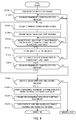
- FIG. 3 is a flowchart illustrating an example of the process of writing data in writing apparatus 10.
- Writing apparatus 10 transmits the factory mode start request to ECU 20 (ST100).
- writing apparatus 10 Upon receipt of the factory mode start response for ST100 from ECU 20, writing apparatus 10 transmits the block transmission start request to ECU 20 (ST102).
- writing apparatus 10 sequentially transmits the frames to ECU 20 (ST104).
- writing apparatus 10 stands by for transmission of the check value for one block from ECU 20 (ST106: NO).
- writing apparatus 10 determines whether the check value for one block transmitted in ST104 coincides with the check value received in ST106 or not (ST108).
- writing apparatus 10 determines whether transmission of all the blocks has been completed or not (ST110).
- writing apparatus 10 transmits the total block verification request to ECU 20 (ST112).
- writing apparatus 10 determines whether the result of the total block verification response is normal or not (ST114).
- writing apparatus 10 transmits the factory mode finishing request to ECU 20 in ST116.
- writing apparatus 10 After receipt of a factory mode finishing response from ECU 20 (ST116), writing apparatus 10 normally finishes the process of writing data.
- FIG. 4 is a flowchart illustrating an example of the process of writing data in CPU 30.
- CPU 30 Upon receipt of the factory mode start request issued by writing apparatus 10, CPU 30 starts the factory mode, and transmits the factory mode start response to writing apparatus 10 (ST200).
- CPU 30 determines whether the block transmission start request has been transmitted from writing apparatus 10 or not (ST202). If the block transmission start request has not been transmitted (ST202: NO), CPU 30 returns the processing to the start of ST202.
- CPU 30 Upon receipt of the block transmission start request (ST202: YES), CPU 30 designates, for DMAC 26, the transfer destination area for 256 ⁇ 16 frames scheduled to be stored in communication buffer 23 (ST204). As described in FIG. 2 , the transfer destination area is alternately switched between RAM first area 50A and RAM second area 50B every time receipt of 16 blocks of data.
- CPU 30 transmits the block transmission start response to writing apparatus 10 (ST206).
- CPU 30 determines whether a notification about completion of transfer for one block from DMAC 26 to the transfer destination area has been transmitted or not (ST208). If the completion notification has not been transmitted (ST208: NO), CPU 30 returns the processing to the start of ST208.
- CPU 30 Upon receipt of the completion notification in ST208 (ST208: YES), CPU 30 calculates the check value of one block of data pertaining to the completion notification (ST210). CPU 30 then transmits the calculated check value to writing apparatus 10.
- CPU 30 determines whether 16 blocks of data have been transferred to the transfer destination area or not (ST212). If the 16 blocks of data have not been transferred to the transfer destination area yet (ST212: NO), CPU 30 returns the processing to ST202, and stands by for incoming transmission of the next block transmission start request.
- CPU 30 determines whether the block transmission start request has been transmitted from writing apparatus 10 or not (ST214).
- CPU 30 Upon receipt of the block transmission start request (ST214: YES), CPU 30 returns the processing to ST204.
- CPU 30 indicates, for DMAC 26, a transfer destination area different from that last time as the transfer destination area for 256 ⁇ 16 frames scheduled to be stored in communication buffer 23. Accordingly, the block pertaining to ST214 is transferred to the switched transfer destination area.
- DMAC 26 Upon receipt of the indication of the transfer destination area different from that last time from CPU 30, DMAC 26 issues, to the flash memory controller, the flash write instruction pertaining to 16 blocks in the last transfer destination area.
- CPU 30 determines whether the total block verification request has been transmitted from writing apparatus 10 or not (ST220).
- CPU 30 Without incoming transmission of the total block verification request by writing apparatus 10 (ST220: NO), CPU 30 abnormally terminates the data writing process. This is because the check value transmitted in ST210 described above can be estimated to be inconsistent if the block transmission start request has not been transmitted from writing apparatus 10 and the total block verification request has not been transmitted. That is, this is because the 16 blocks of data stored in the transfer destination area can be estimated to include an error.
- CPU 30 Upon receipt of the total block verification request from writing apparatus 10 (ST220: YES), CPU 30 stands by for incoming transmission of the completion notification about the flash write process pertaining to the final block from the flash memory controller (ST222).
- CPU 30 After receipt of the completion notification about the flash write process pertaining to the final block, CPU 30 verifies the entire data written in flash memory 28, and transmits the verification result to writing apparatus 10 (ST224).
- the verification result includes any of "normal” or "abnormal.”
- CPU 30 transmits the factory mode finishing response to writing apparatus 10, and finishes the factory mode (ST226).
- Reduction in the amount of data transmission from writing apparatus 10 to ECU 20 can further reduce the time required for the transmission.
- An example is hereinafter described.
- item data length a part that does not reach the data length is filled with predetermined data (for example, '0xFF”) (that is, subjected to padding).
- Writing apparatus 10 adds the substantial length of data on each item (called “substantial data length") to the beginning of the data, and removes the padding data. Writing apparatus 10 then couples the data items, from which the padding data has been removed, to each other, divides the coupled data into blocks and frames as illustrated in FIG. 2 , and sequentially transmits the blocks and frames to ECU 20.
- ECU 20 having received the coupled data refers to the substantial data length, and extracts item data. ECU 20 then applies padding to the part that does not reach the item data length, and writes the data into flash memory 28.
- the substantial data length is smaller than the padded data length. Accordingly, the amount of data transmission from writing apparatus 10 to ECU 20, that is, the time required for the transmission is further reduced. As a result, the entire time required for the process of writing data into flash memory 28 included in ECU 20 is further reduced.
- CPU 30 can execute the transfer destination area switching, and start of writing into flash memory 28, triggered by reception of the block transmission start request that is information for making a query of apparatus 10 and CPU 30 is negated. As a result, the time required for data transmission from writing apparatus 10 to ECU 20 is reduced.
- Writing apparatus 10 checks the corruption of the data block based on the check value transmitted from CPU 30, thereby reducing the processing load on CPU 30.
- the process of writing the data stored in RAM first area 50A or RAM second area 50B into flash memory 28, and the process of transferring the data transmitted from writing apparatus 10 to RAM first area 50A or RAM second area 50B can be executed in parallel.
- This disclosure can be used for a control apparatus for a vehicle.
Landscapes
- Engineering & Computer Science (AREA)
- Theoretical Computer Science (AREA)
- General Engineering & Computer Science (AREA)
- Physics & Mathematics (AREA)
- General Physics & Mathematics (AREA)
- Human Computer Interaction (AREA)
- Combustion & Propulsion (AREA)
- Chemical & Material Sciences (AREA)
- Quality & Reliability (AREA)
- Mechanical Engineering (AREA)
- Techniques For Improving Reliability Of Storages (AREA)
- Combined Controls Of Internal Combustion Engines (AREA)
- Detection And Correction Of Errors (AREA)
- Bus Control (AREA)
- Memory System (AREA)
- Communication Control (AREA)
Claims (3)
- Appareil de commande, comprenant :une première section de mémorisation ;une seconde section de mémorisation, laquelle présente un débit d'entrée et de sortie supérieur à celui de la première section de mémorisation, la seconde section de mémorisation comprenant une première zone de mémorisation et une seconde zone de mémorisation aptes à la mémorisation d'un nombre prédéfini de blocs de données ; etune section de commande, laquelle effectue la commande du paramétrage de la première ou de la seconde zone de mémorisation en tant que zone de mémorisation de destination de transfert, mémorisant le bloc de données transmis à partir d'un appareil d'écriture dans la zone de mémorisation de destination de transfert et la transmission d'une valeur de vérification du bloc de données à l'appareil d'écriture,dans lequel l'appareil d'écriture détermine si la valeur de vérification transmise à partir de la section de commande est appropriée ou non et transmet une demande de début de transmission de bloc à la section de commande avant la transmission d'un bloc de données suivant dans un cas où l'appareil d'écriture détermine que la valeur de vérification est appropriée, etdans lequel, lorsque le nombre prédéfini de blocs de données est mémorisé dans la zone de mémorisation de destination de transfert et la demande de début de transmission de bloc est reçue de l'appareil d'écriture, la section de commande commute la zone de mémorisation de destination de transfert vers une autre des première et seconde zones de mémorisation pour mémoriser le bloc de données suivant, transmis de l'appareil d'écriture dans la zone de mémorisation de destination de transfert et pour transmettre une valeur de vérification du bloc de données suivant à l'appareil d'écriture et amène le nombre prédéfini de blocs de données mémorisés dans la zone de mémorisation de destination de transfert, laquelle est ladite des zones de mémorisation avant la commutation, à être écris dans la première section de mémorisation en parallèle avec la détermination de la valeur de vérification du bloc suivant de données par l'appareil d'écriture.
- Appareil de commande selon la revendication 1, dans lequel l'appareil d'écriture divise le bloc de données en une pluralité de trames et transmet lesdites trames,
dans lequel l'appareil de commande comprend en outre un dispositif de commande de DMA, lequel transfère de manière séquentielle les trames reçues vers la zone de mémorisation de destination de transfert et lequel notifie à la section de commande une notification d'achèvement de l'achèvement du transfert d'un bloc de données dans le cas de l'achèvement, et
dans lequel la section de commande reçoit la notification d'achèvement du dispositif de commande de DMA et transmet la valeur de vérification se rapportant au bloc de données à l'appareil d'écriture. - Procédé d'écriture de données sur un appareil de commande,
dans lequel l'appareil de commande comprend : une première section de mémorisation ; et une seconde section de mémorisation, laquelle présente un débit d'entrée et de sortie supérieur à celui de la première section de mémorisation, la seconde section de mémorisation comprenant une première zone de mémorisation et une seconde zone de mémorisation, lesquelles sont aptes à la mémorisation d'un nombre prédéfini de blocs de données,
dans lequel un appareil d'écriture transmet le bloc de données à l'appareil de commande,
dans lequel l'appareil de commande définit la première ou la seconde zone de mémorisation en tant que zone de mémorisation de destination de transfert, mémorise le bloc de données transmis à partir de l'appareil d'écriture dans la zone de mémorisation de destination de transfert et transmet une valeur de vérification du bloc de données à l'appareil d'écriture,
dans lequel l'appareil d'écriture détermine si la valeur de vérification transmise par l'appareil de commande est appropriée ou non et transmet une demande de début de transmission de bloc à l'appareil de commande avant la transmission d'un bloc de données suivant dans un cas où l'appareil d'écriture détermine que la valeur de vérification est appropriée, et
dans lequel, lorsque le nombre prédéfini de blocs de données est mémorisé dans la zone de mémorisation de destination de transfert et la demande de début de transmission de bloc est reçue de l'appareil d'écriture, l'appareil de commande commute la zone de mémorisation de destination de transfert vers une autre des première et seconde zones de mémorisation, pour mémoriser le bloc de données suivant transmis de l'appareil d'écriture à la zone de mémorisation de destination de transfert, pour transmettre une valeur de vérification du bloc de données suivant à l'appareil d'écriture et amène le nombre prédéfini de blocs de données mémorisé dans la zone de mémorisation de destination de transfert, laquelle est ladite des zones de mémorisation avant la commutation à être écris dans la première section de mémorisation, en parallèle avec la détermination de la valeur de vérification du bloc suivant de données par l'appareil d'écriture.
Applications Claiming Priority (2)
| Application Number | Priority Date | Filing Date | Title |
|---|---|---|---|
| JP2016237752A JP6935190B2 (ja) | 2016-12-07 | 2016-12-07 | 制御装置、及び、制御装置へのデータ書き込み方法 |
| PCT/JP2017/043575 WO2018105587A1 (fr) | 2016-12-07 | 2017-12-05 | Dispositif de commande et procédé d'écriture de données dans un tel dispositif de commande |
Publications (3)
| Publication Number | Publication Date |
|---|---|
| EP3553660A1 EP3553660A1 (fr) | 2019-10-16 |
| EP3553660A4 EP3553660A4 (fr) | 2019-11-20 |
| EP3553660B1 true EP3553660B1 (fr) | 2021-02-03 |
Family
ID=62491943
Family Applications (1)
| Application Number | Title | Priority Date | Filing Date |
|---|---|---|---|
| EP17879532.4A Active EP3553660B1 (fr) | 2016-12-07 | 2017-12-05 | Dispositif de commande et procédé d'écriture de données dans un tel dispositif de commande |
Country Status (5)
| Country | Link |
|---|---|
| US (1) | US20190339910A1 (fr) |
| EP (1) | EP3553660B1 (fr) |
| JP (1) | JP6935190B2 (fr) |
| CN (1) | CN110050262B (fr) |
| WO (1) | WO2018105587A1 (fr) |
Families Citing this family (5)
| Publication number | Priority date | Publication date | Assignee | Title |
|---|---|---|---|---|
| KR102075086B1 (ko) * | 2018-11-13 | 2020-02-07 | 현대오트론 주식회사 | Dma를 활용한 epm 마이크로틱 생성 긴급 중단 방법 |
| US12086582B2 (en) * | 2019-08-05 | 2024-09-10 | Hitachi Astemo, Ltd. | Vehicle controller, updated program, program updating system, and writing device |
| CN112802518B (zh) * | 2021-03-25 | 2021-07-02 | 深圳市汇顶科技股份有限公司 | 数据写入方法、片上系统芯片及计算机可读存储介质 |
| JP2024106650A (ja) * | 2023-01-27 | 2024-08-08 | トヨタ自動車株式会社 | 情報処理装置及び情報処理方法 |
| WO2024195417A1 (fr) * | 2023-03-23 | 2024-09-26 | 富士通株式会社 | Dispositif de transmission optique et procédé de transmission optique |
Family Cites Families (10)
| Publication number | Priority date | Publication date | Assignee | Title |
|---|---|---|---|---|
| JP3545659B2 (ja) * | 1999-10-21 | 2004-07-21 | 松下電器産業株式会社 | プログラム更新方法および通信端末装置 |
| JP2005135260A (ja) * | 2003-10-31 | 2005-05-26 | Fujitsu Ten Ltd | 製品機能設定方法及び製品機能設定システム |
| JP2005337017A (ja) * | 2004-05-24 | 2005-12-08 | Mitsubishi Electric Corp | 車両用電子制御装置 |
| JP2007286813A (ja) * | 2006-04-14 | 2007-11-01 | Sony Corp | メモリ制御装置、メモリ制御方法 |
| JP4532450B2 (ja) * | 2006-09-06 | 2010-08-25 | 株式会社デンソー | エンジン制御用データの処理装置及びエンジン制御装置 |
| US8458377B2 (en) * | 2010-03-05 | 2013-06-04 | Lsi Corporation | DMA engine capable of concurrent data manipulation |
| JP2013068105A (ja) * | 2011-09-21 | 2013-04-18 | Hitachi Automotive Systems Ltd | 自動車用電子制御装置 |
| JP5451705B2 (ja) * | 2011-09-21 | 2014-03-26 | 日立オートモティブシステムズ株式会社 | 自動車用電子制御装置及びデータ通信方法 |
| US10402251B2 (en) * | 2015-07-24 | 2019-09-03 | Nxp Usa, Inc. | DMA controller for a data processing system, a data processing system and a method of operating a DMA controller |
| JP2018028830A (ja) * | 2016-08-19 | 2018-02-22 | 三菱電機株式会社 | 電子制御装置およびその情報記憶方法 |
-
2016
- 2016-12-07 JP JP2016237752A patent/JP6935190B2/ja active Active
-
2017
- 2017-12-05 EP EP17879532.4A patent/EP3553660B1/fr active Active
- 2017-12-05 WO PCT/JP2017/043575 patent/WO2018105587A1/fr not_active Ceased
- 2017-12-05 CN CN201780075699.XA patent/CN110050262B/zh active Active
- 2017-12-05 US US16/467,510 patent/US20190339910A1/en not_active Abandoned
Non-Patent Citations (1)
| Title |
|---|
| None * |
Also Published As
| Publication number | Publication date |
|---|---|
| CN110050262A (zh) | 2019-07-23 |
| EP3553660A1 (fr) | 2019-10-16 |
| JP2018092542A (ja) | 2018-06-14 |
| JP6935190B2 (ja) | 2021-09-15 |
| US20190339910A1 (en) | 2019-11-07 |
| CN110050262B (zh) | 2023-09-15 |
| EP3553660A4 (fr) | 2019-11-20 |
| WO2018105587A1 (fr) | 2018-06-14 |
Similar Documents
| Publication | Publication Date | Title |
|---|---|---|
| EP3553660B1 (fr) | Dispositif de commande et procédé d'écriture de données dans un tel dispositif de commande | |
| US20010032301A1 (en) | Multiplexed computer system | |
| US7831755B2 (en) | Method and system for interfacing a plurality of memory devices using an MMC/SD protocol | |
| US5436732A (en) | Image data processing system | |
| EP0734139A2 (fr) | Dispositif de transfert de données avec contrÔle d'ensemble d'ordinateurs | |
| JP2001514780A (ja) | 再帰的マルチチャネルインターフェース | |
| US20050041606A1 (en) | Data communication apparatus, data communication method, data communication program and recording medium in which data communication program was recorded | |
| US20140218774A1 (en) | Image Forming Apparatus that Buffers Data in a Storage Device and Reduces Delays in Process | |
| JPH0282846A (ja) | バッファプール事前拡張装置 | |
| JPS5824253A (ja) | パケツト合成方式 | |
| CN113868164B (zh) | 一种双机通信方法、装置和系统 | |
| JP3001560B1 (ja) | Tdma方式移動体通信システム | |
| JPH1027231A (ja) | Icカード | |
| JP4774620B2 (ja) | 情報通信方法及び情報通信システム | |
| JPH05324342A (ja) | プログラムロード方法 | |
| CN117667810A (zh) | 数据传输方法、装置和通信系统 | |
| JP2527066B2 (ja) | 受信待ち行列処理装置 | |
| CN114422590A (zh) | 一种gpu云服务器迁移至本地的通信系统及通信方法 | |
| JPH05292086A (ja) | 高負荷試験方式 | |
| JP3764829B2 (ja) | ファクシミリ装置 | |
| JP4680440B2 (ja) | シリアル送信装置及びシリアル送信装置の送信バッファリング制御方法 | |
| JP2001043198A (ja) | システム間通信制御方式 | |
| JPH04336653A (ja) | メモリ制御方法 | |
| CN116614562A (zh) | 一种高效的数据传输方法及数据传输系统 | |
| JPH08293875A (ja) | Lanのスイッチング装置 |
Legal Events
| Date | Code | Title | Description |
|---|---|---|---|
| STAA | Information on the status of an ep patent application or granted ep patent |
Free format text: STATUS: THE INTERNATIONAL PUBLICATION HAS BEEN MADE |
|
| PUAI | Public reference made under article 153(3) epc to a published international application that has entered the european phase |
Free format text: ORIGINAL CODE: 0009012 |
|
| STAA | Information on the status of an ep patent application or granted ep patent |
Free format text: STATUS: REQUEST FOR EXAMINATION WAS MADE |
|
| 17P | Request for examination filed |
Effective date: 20190606 |
|
| AK | Designated contracting states |
Kind code of ref document: A1 Designated state(s): AL AT BE BG CH CY CZ DE DK EE ES FI FR GB GR HR HU IE IS IT LI LT LU LV MC MK MT NL NO PL PT RO RS SE SI SK SM TR |
|
| AX | Request for extension of the european patent |
Extension state: BA ME |
|
| A4 | Supplementary search report drawn up and despatched |
Effective date: 20191023 |
|
| RIC1 | Information provided on ipc code assigned before grant |
Ipc: F02D 41/24 20060101ALI20191017BHEP Ipc: G06F 13/28 20060101ALI20191017BHEP Ipc: F02D 45/00 20060101ALI20191017BHEP Ipc: G06F 3/06 20060101ALI20191017BHEP Ipc: G06F 12/00 20060101ALI20191017BHEP Ipc: G06F 11/10 20060101AFI20191017BHEP |
|
| DAV | Request for validation of the european patent (deleted) | ||
| DAX | Request for extension of the european patent (deleted) | ||
| GRAP | Despatch of communication of intention to grant a patent |
Free format text: ORIGINAL CODE: EPIDOSNIGR1 |
|
| STAA | Information on the status of an ep patent application or granted ep patent |
Free format text: STATUS: GRANT OF PATENT IS INTENDED |
|
| RIC1 | Information provided on ipc code assigned before grant |
Ipc: G06F 12/00 20060101ALI20200710BHEP Ipc: G06F 3/06 20060101ALI20200710BHEP Ipc: F02D 41/24 20060101ALI20200710BHEP Ipc: G06F 11/10 20060101AFI20200710BHEP Ipc: F02D 45/00 20060101ALI20200710BHEP Ipc: G06F 13/28 20060101ALI20200710BHEP |
|
| INTG | Intention to grant announced |
Effective date: 20200810 |
|
| GRAS | Grant fee paid |
Free format text: ORIGINAL CODE: EPIDOSNIGR3 |
|
| GRAA | (expected) grant |
Free format text: ORIGINAL CODE: 0009210 |
|
| STAA | Information on the status of an ep patent application or granted ep patent |
Free format text: STATUS: THE PATENT HAS BEEN GRANTED |
|
| AK | Designated contracting states |
Kind code of ref document: B1 Designated state(s): AL AT BE BG CH CY CZ DE DK EE ES FI FR GB GR HR HU IE IS IT LI LT LU LV MC MK MT NL NO PL PT RO RS SE SI SK SM TR |
|
| REG | Reference to a national code |
Ref country code: GB Ref legal event code: FG4D |
|
| REG | Reference to a national code |
Ref country code: AT Ref legal event code: REF Ref document number: 1359848 Country of ref document: AT Kind code of ref document: T Effective date: 20210215 Ref country code: CH Ref legal event code: EP |
|
| REG | Reference to a national code |
Ref country code: DE Ref legal event code: R096 Ref document number: 602017032433 Country of ref document: DE |
|
| REG | Reference to a national code |
Ref country code: IE Ref legal event code: FG4D |
|
| REG | Reference to a national code |
Ref country code: NL Ref legal event code: MP Effective date: 20210203 |
|
| REG | Reference to a national code |
Ref country code: LT Ref legal event code: MG9D |
|
| REG | Reference to a national code |
Ref country code: AT Ref legal event code: MK05 Ref document number: 1359848 Country of ref document: AT Kind code of ref document: T Effective date: 20210203 |
|
| PG25 | Lapsed in a contracting state [announced via postgrant information from national office to epo] |
Ref country code: FI Free format text: LAPSE BECAUSE OF FAILURE TO SUBMIT A TRANSLATION OF THE DESCRIPTION OR TO PAY THE FEE WITHIN THE PRESCRIBED TIME-LIMIT Effective date: 20210203 Ref country code: GR Free format text: LAPSE BECAUSE OF FAILURE TO SUBMIT A TRANSLATION OF THE DESCRIPTION OR TO PAY THE FEE WITHIN THE PRESCRIBED TIME-LIMIT Effective date: 20210504 Ref country code: HR Free format text: LAPSE BECAUSE OF FAILURE TO SUBMIT A TRANSLATION OF THE DESCRIPTION OR TO PAY THE FEE WITHIN THE PRESCRIBED TIME-LIMIT Effective date: 20210203 Ref country code: PT Free format text: LAPSE BECAUSE OF FAILURE TO SUBMIT A TRANSLATION OF THE DESCRIPTION OR TO PAY THE FEE WITHIN THE PRESCRIBED TIME-LIMIT Effective date: 20210604 Ref country code: NO Free format text: LAPSE BECAUSE OF FAILURE TO SUBMIT A TRANSLATION OF THE DESCRIPTION OR TO PAY THE FEE WITHIN THE PRESCRIBED TIME-LIMIT Effective date: 20210503 Ref country code: BG Free format text: LAPSE BECAUSE OF FAILURE TO SUBMIT A TRANSLATION OF THE DESCRIPTION OR TO PAY THE FEE WITHIN THE PRESCRIBED TIME-LIMIT Effective date: 20210503 Ref country code: LT Free format text: LAPSE BECAUSE OF FAILURE TO SUBMIT A TRANSLATION OF THE DESCRIPTION OR TO PAY THE FEE WITHIN THE PRESCRIBED TIME-LIMIT Effective date: 20210203 |
|
| PG25 | Lapsed in a contracting state [announced via postgrant information from national office to epo] |
Ref country code: AT Free format text: LAPSE BECAUSE OF FAILURE TO SUBMIT A TRANSLATION OF THE DESCRIPTION OR TO PAY THE FEE WITHIN THE PRESCRIBED TIME-LIMIT Effective date: 20210203 Ref country code: RS Free format text: LAPSE BECAUSE OF FAILURE TO SUBMIT A TRANSLATION OF THE DESCRIPTION OR TO PAY THE FEE WITHIN THE PRESCRIBED TIME-LIMIT Effective date: 20210203 Ref country code: LV Free format text: LAPSE BECAUSE OF FAILURE TO SUBMIT A TRANSLATION OF THE DESCRIPTION OR TO PAY THE FEE WITHIN THE PRESCRIBED TIME-LIMIT Effective date: 20210203 Ref country code: NL Free format text: LAPSE BECAUSE OF FAILURE TO SUBMIT A TRANSLATION OF THE DESCRIPTION OR TO PAY THE FEE WITHIN THE PRESCRIBED TIME-LIMIT Effective date: 20210203 Ref country code: PL Free format text: LAPSE BECAUSE OF FAILURE TO SUBMIT A TRANSLATION OF THE DESCRIPTION OR TO PAY THE FEE WITHIN THE PRESCRIBED TIME-LIMIT Effective date: 20210203 Ref country code: SE Free format text: LAPSE BECAUSE OF FAILURE TO SUBMIT A TRANSLATION OF THE DESCRIPTION OR TO PAY THE FEE WITHIN THE PRESCRIBED TIME-LIMIT Effective date: 20210203 |
|
| PG25 | Lapsed in a contracting state [announced via postgrant information from national office to epo] |
Ref country code: IS Free format text: LAPSE BECAUSE OF FAILURE TO SUBMIT A TRANSLATION OF THE DESCRIPTION OR TO PAY THE FEE WITHIN THE PRESCRIBED TIME-LIMIT Effective date: 20210603 |
|
| PG25 | Lapsed in a contracting state [announced via postgrant information from national office to epo] |
Ref country code: SM Free format text: LAPSE BECAUSE OF FAILURE TO SUBMIT A TRANSLATION OF THE DESCRIPTION OR TO PAY THE FEE WITHIN THE PRESCRIBED TIME-LIMIT Effective date: 20210203 Ref country code: CZ Free format text: LAPSE BECAUSE OF FAILURE TO SUBMIT A TRANSLATION OF THE DESCRIPTION OR TO PAY THE FEE WITHIN THE PRESCRIBED TIME-LIMIT Effective date: 20210203 Ref country code: EE Free format text: LAPSE BECAUSE OF FAILURE TO SUBMIT A TRANSLATION OF THE DESCRIPTION OR TO PAY THE FEE WITHIN THE PRESCRIBED TIME-LIMIT Effective date: 20210203 |
|
| REG | Reference to a national code |
Ref country code: DE Ref legal event code: R097 Ref document number: 602017032433 Country of ref document: DE |
|
| PG25 | Lapsed in a contracting state [announced via postgrant information from national office to epo] |
Ref country code: RO Free format text: LAPSE BECAUSE OF FAILURE TO SUBMIT A TRANSLATION OF THE DESCRIPTION OR TO PAY THE FEE WITHIN THE PRESCRIBED TIME-LIMIT Effective date: 20210203 Ref country code: SK Free format text: LAPSE BECAUSE OF FAILURE TO SUBMIT A TRANSLATION OF THE DESCRIPTION OR TO PAY THE FEE WITHIN THE PRESCRIBED TIME-LIMIT Effective date: 20210203 Ref country code: DK Free format text: LAPSE BECAUSE OF FAILURE TO SUBMIT A TRANSLATION OF THE DESCRIPTION OR TO PAY THE FEE WITHIN THE PRESCRIBED TIME-LIMIT Effective date: 20210203 |
|
| PLBE | No opposition filed within time limit |
Free format text: ORIGINAL CODE: 0009261 |
|
| STAA | Information on the status of an ep patent application or granted ep patent |
Free format text: STATUS: NO OPPOSITION FILED WITHIN TIME LIMIT |
|
| 26N | No opposition filed |
Effective date: 20211104 |
|
| PG25 | Lapsed in a contracting state [announced via postgrant information from national office to epo] |
Ref country code: ES Free format text: LAPSE BECAUSE OF FAILURE TO SUBMIT A TRANSLATION OF THE DESCRIPTION OR TO PAY THE FEE WITHIN THE PRESCRIBED TIME-LIMIT Effective date: 20210203 Ref country code: AL Free format text: LAPSE BECAUSE OF FAILURE TO SUBMIT A TRANSLATION OF THE DESCRIPTION OR TO PAY THE FEE WITHIN THE PRESCRIBED TIME-LIMIT Effective date: 20210203 |
|
| PG25 | Lapsed in a contracting state [announced via postgrant information from national office to epo] |
Ref country code: SI Free format text: LAPSE BECAUSE OF FAILURE TO SUBMIT A TRANSLATION OF THE DESCRIPTION OR TO PAY THE FEE WITHIN THE PRESCRIBED TIME-LIMIT Effective date: 20210203 |
|
| PG25 | Lapsed in a contracting state [announced via postgrant information from national office to epo] |
Ref country code: IT Free format text: LAPSE BECAUSE OF FAILURE TO SUBMIT A TRANSLATION OF THE DESCRIPTION OR TO PAY THE FEE WITHIN THE PRESCRIBED TIME-LIMIT Effective date: 20210203 |
|
| PG25 | Lapsed in a contracting state [announced via postgrant information from national office to epo] |
Ref country code: IS Free format text: LAPSE BECAUSE OF FAILURE TO SUBMIT A TRANSLATION OF THE DESCRIPTION OR TO PAY THE FEE WITHIN THE PRESCRIBED TIME-LIMIT Effective date: 20210603 |
|
| PG25 | Lapsed in a contracting state [announced via postgrant information from national office to epo] |
Ref country code: MC Free format text: LAPSE BECAUSE OF FAILURE TO SUBMIT A TRANSLATION OF THE DESCRIPTION OR TO PAY THE FEE WITHIN THE PRESCRIBED TIME-LIMIT Effective date: 20210203 |
|
| REG | Reference to a national code |
Ref country code: CH Ref legal event code: PL |
|
| REG | Reference to a national code |
Ref country code: BE Ref legal event code: MM Effective date: 20211231 |
|
| PG25 | Lapsed in a contracting state [announced via postgrant information from national office to epo] |
Ref country code: LU Free format text: LAPSE BECAUSE OF NON-PAYMENT OF DUE FEES Effective date: 20211205 Ref country code: IE Free format text: LAPSE BECAUSE OF NON-PAYMENT OF DUE FEES Effective date: 20211205 |
|
| PG25 | Lapsed in a contracting state [announced via postgrant information from national office to epo] |
Ref country code: BE Free format text: LAPSE BECAUSE OF NON-PAYMENT OF DUE FEES Effective date: 20211231 |
|
| PG25 | Lapsed in a contracting state [announced via postgrant information from national office to epo] |
Ref country code: LI Free format text: LAPSE BECAUSE OF NON-PAYMENT OF DUE FEES Effective date: 20211231 Ref country code: CH Free format text: LAPSE BECAUSE OF NON-PAYMENT OF DUE FEES Effective date: 20211231 |
|
| PGFP | Annual fee paid to national office [announced via postgrant information from national office to epo] |
Ref country code: GB Payment date: 20221223 Year of fee payment: 6 Ref country code: FR Payment date: 20221222 Year of fee payment: 6 |
|
| PG25 | Lapsed in a contracting state [announced via postgrant information from national office to epo] |
Ref country code: CY Free format text: LAPSE BECAUSE OF FAILURE TO SUBMIT A TRANSLATION OF THE DESCRIPTION OR TO PAY THE FEE WITHIN THE PRESCRIBED TIME-LIMIT Effective date: 20210203 |
|
| PG25 | Lapsed in a contracting state [announced via postgrant information from national office to epo] |
Ref country code: HU Free format text: LAPSE BECAUSE OF FAILURE TO SUBMIT A TRANSLATION OF THE DESCRIPTION OR TO PAY THE FEE WITHIN THE PRESCRIBED TIME-LIMIT; INVALID AB INITIO Effective date: 20171205 |
|
| PG25 | Lapsed in a contracting state [announced via postgrant information from national office to epo] |
Ref country code: MK Free format text: LAPSE BECAUSE OF FAILURE TO SUBMIT A TRANSLATION OF THE DESCRIPTION OR TO PAY THE FEE WITHIN THE PRESCRIBED TIME-LIMIT Effective date: 20210203 |
|
| GBPC | Gb: european patent ceased through non-payment of renewal fee |
Effective date: 20231205 |
|
| PG25 | Lapsed in a contracting state [announced via postgrant information from national office to epo] |
Ref country code: MT Free format text: LAPSE BECAUSE OF FAILURE TO SUBMIT A TRANSLATION OF THE DESCRIPTION OR TO PAY THE FEE WITHIN THE PRESCRIBED TIME-LIMIT Effective date: 20210203 |
|
| PG25 | Lapsed in a contracting state [announced via postgrant information from national office to epo] |
Ref country code: GB Free format text: LAPSE BECAUSE OF NON-PAYMENT OF DUE FEES Effective date: 20231205 |
|
| PG25 | Lapsed in a contracting state [announced via postgrant information from national office to epo] |
Ref country code: FR Free format text: LAPSE BECAUSE OF NON-PAYMENT OF DUE FEES Effective date: 20231231 |
|
| PG25 | Lapsed in a contracting state [announced via postgrant information from national office to epo] |
Ref country code: GB Free format text: LAPSE BECAUSE OF NON-PAYMENT OF DUE FEES Effective date: 20231205 Ref country code: FR Free format text: LAPSE BECAUSE OF NON-PAYMENT OF DUE FEES Effective date: 20231231 |
|
| PG25 | Lapsed in a contracting state [announced via postgrant information from national office to epo] |
Ref country code: TR Free format text: LAPSE BECAUSE OF FAILURE TO SUBMIT A TRANSLATION OF THE DESCRIPTION OR TO PAY THE FEE WITHIN THE PRESCRIBED TIME-LIMIT Effective date: 20210203 |
|
| PGFP | Annual fee paid to national office [announced via postgrant information from national office to epo] |
Ref country code: DE Payment date: 20251126 Year of fee payment: 9 |