EP3547381B1 - Verfahren zur regulierung und steuerung des phasenwechsels eines wasserstoffhaltigen übergangsmetalloxids - Google Patents
Verfahren zur regulierung und steuerung des phasenwechsels eines wasserstoffhaltigen übergangsmetalloxids Download PDFInfo
- Publication number
- EP3547381B1 EP3547381B1 EP17874222.7A EP17874222A EP3547381B1 EP 3547381 B1 EP3547381 B1 EP 3547381B1 EP 17874222 A EP17874222 A EP 17874222A EP 3547381 B1 EP3547381 B1 EP 3547381B1
- Authority
- EP
- European Patent Office
- Prior art keywords
- transition metal
- metal oxide
- hydrogen
- phase
- containing transition
- Prior art date
- Legal status (The legal status is an assumption and is not a legal conclusion. Google has not performed a legal analysis and makes no representation as to the accuracy of the status listed.)
- Active
Links
Images






Classifications
-
- H—ELECTRICITY
- H10—SEMICONDUCTOR DEVICES; ELECTRIC SOLID-STATE DEVICES NOT OTHERWISE PROVIDED FOR
- H10N—ELECTRIC SOLID-STATE DEVICES NOT OTHERWISE PROVIDED FOR
- H10N70/00—Solid-state devices having no potential barriers, and specially adapted for rectifying, amplifying, oscillating or switching
- H10N70/20—Multistable switching devices, e.g. memristors
- H10N70/231—Multistable switching devices, e.g. memristors based on solid-state phase change, e.g. between amorphous and crystalline phases, Ovshinsky effect
-
- G—PHYSICS
- G02—OPTICS
- G02F—OPTICAL DEVICES OR ARRANGEMENTS FOR THE CONTROL OF LIGHT BY MODIFICATION OF THE OPTICAL PROPERTIES OF THE MEDIA OF THE ELEMENTS INVOLVED THEREIN; NON-LINEAR OPTICS; FREQUENCY-CHANGING OF LIGHT; OPTICAL LOGIC ELEMENTS; OPTICAL ANALOGUE/DIGITAL CONVERTERS
- G02F1/00—Devices or arrangements for the control of the intensity, colour, phase, polarisation or direction of light arriving from an independent light source, e.g. switching, gating or modulating; Non-linear optics
- G02F1/01—Devices or arrangements for the control of the intensity, colour, phase, polarisation or direction of light arriving from an independent light source, e.g. switching, gating or modulating; Non-linear optics for the control of the intensity, phase, polarisation or colour
- G02F1/15—Devices or arrangements for the control of the intensity, colour, phase, polarisation or direction of light arriving from an independent light source, e.g. switching, gating or modulating; Non-linear optics for the control of the intensity, phase, polarisation or colour based on an electrochromic effect
- G02F1/1514—Devices or arrangements for the control of the intensity, colour, phase, polarisation or direction of light arriving from an independent light source, e.g. switching, gating or modulating; Non-linear optics for the control of the intensity, phase, polarisation or colour based on an electrochromic effect characterised by the electrochromic material, e.g. by the electrodeposited material
- G02F1/1523—Devices or arrangements for the control of the intensity, colour, phase, polarisation or direction of light arriving from an independent light source, e.g. switching, gating or modulating; Non-linear optics for the control of the intensity, phase, polarisation or colour based on an electrochromic effect characterised by the electrochromic material, e.g. by the electrodeposited material comprising inorganic material
- G02F1/1524—Transition metal compounds
-
- G—PHYSICS
- G02—OPTICS
- G02F—OPTICAL DEVICES OR ARRANGEMENTS FOR THE CONTROL OF LIGHT BY MODIFICATION OF THE OPTICAL PROPERTIES OF THE MEDIA OF THE ELEMENTS INVOLVED THEREIN; NON-LINEAR OPTICS; FREQUENCY-CHANGING OF LIGHT; OPTICAL LOGIC ELEMENTS; OPTICAL ANALOGUE/DIGITAL CONVERTERS
- G02F1/00—Devices or arrangements for the control of the intensity, colour, phase, polarisation or direction of light arriving from an independent light source, e.g. switching, gating or modulating; Non-linear optics
- G02F1/01—Devices or arrangements for the control of the intensity, colour, phase, polarisation or direction of light arriving from an independent light source, e.g. switching, gating or modulating; Non-linear optics for the control of the intensity, phase, polarisation or colour
- G02F1/15—Devices or arrangements for the control of the intensity, colour, phase, polarisation or direction of light arriving from an independent light source, e.g. switching, gating or modulating; Non-linear optics for the control of the intensity, phase, polarisation or colour based on an electrochromic effect
- G02F1/1514—Devices or arrangements for the control of the intensity, colour, phase, polarisation or direction of light arriving from an independent light source, e.g. switching, gating or modulating; Non-linear optics for the control of the intensity, phase, polarisation or colour based on an electrochromic effect characterised by the electrochromic material, e.g. by the electrodeposited material
- G02F1/1523—Devices or arrangements for the control of the intensity, colour, phase, polarisation or direction of light arriving from an independent light source, e.g. switching, gating or modulating; Non-linear optics for the control of the intensity, phase, polarisation or colour based on an electrochromic effect characterised by the electrochromic material, e.g. by the electrodeposited material comprising inorganic material
- G02F1/1525—Devices or arrangements for the control of the intensity, colour, phase, polarisation or direction of light arriving from an independent light source, e.g. switching, gating or modulating; Non-linear optics for the control of the intensity, phase, polarisation or colour based on an electrochromic effect characterised by the electrochromic material, e.g. by the electrodeposited material comprising inorganic material characterised by a particular ion transporting layer, e.g. electrolyte
-
- G—PHYSICS
- G02—OPTICS
- G02F—OPTICAL DEVICES OR ARRANGEMENTS FOR THE CONTROL OF LIGHT BY MODIFICATION OF THE OPTICAL PROPERTIES OF THE MEDIA OF THE ELEMENTS INVOLVED THEREIN; NON-LINEAR OPTICS; FREQUENCY-CHANGING OF LIGHT; OPTICAL LOGIC ELEMENTS; OPTICAL ANALOGUE/DIGITAL CONVERTERS
- G02F1/00—Devices or arrangements for the control of the intensity, colour, phase, polarisation or direction of light arriving from an independent light source, e.g. switching, gating or modulating; Non-linear optics
- G02F1/01—Devices or arrangements for the control of the intensity, colour, phase, polarisation or direction of light arriving from an independent light source, e.g. switching, gating or modulating; Non-linear optics for the control of the intensity, phase, polarisation or colour
- G02F1/15—Devices or arrangements for the control of the intensity, colour, phase, polarisation or direction of light arriving from an independent light source, e.g. switching, gating or modulating; Non-linear optics for the control of the intensity, phase, polarisation or colour based on an electrochromic effect
- G02F1/153—Constructional details
- G02F1/155—Electrodes
-
- H—ELECTRICITY
- H10—SEMICONDUCTOR DEVICES; ELECTRIC SOLID-STATE DEVICES NOT OTHERWISE PROVIDED FOR
- H10D—INORGANIC ELECTRIC SEMICONDUCTOR DEVICES
- H10D84/00—Integrated devices formed in or on semiconductor substrates that comprise only semiconducting layers, e.g. on Si wafers or on GaAs-on-Si wafers
- H10D84/01—Manufacture or treatment
- H10D84/0123—Integrating together multiple components covered by H10D12/00 or H10D30/00, e.g. integrating multiple IGBTs
- H10D84/0126—Integrating together multiple components covered by H10D12/00 or H10D30/00, e.g. integrating multiple IGBTs the components including insulated gates, e.g. IGFETs
- H10D84/0135—Manufacturing their gate conductors
- H10D84/014—Manufacturing their gate conductors the gate conductors having different materials or different implants
-
- H—ELECTRICITY
- H10—SEMICONDUCTOR DEVICES; ELECTRIC SOLID-STATE DEVICES NOT OTHERWISE PROVIDED FOR
- H10D—INORGANIC ELECTRIC SEMICONDUCTOR DEVICES
- H10D84/00—Integrated devices formed in or on semiconductor substrates that comprise only semiconducting layers, e.g. on Si wafers or on GaAs-on-Si wafers
- H10D84/01—Manufacture or treatment
- H10D84/02—Manufacture or treatment characterised by using material-based technologies
- H10D84/03—Manufacture or treatment characterised by using material-based technologies using Group IV technology, e.g. silicon technology or silicon-carbide [SiC] technology
- H10D84/038—Manufacture or treatment characterised by using material-based technologies using Group IV technology, e.g. silicon technology or silicon-carbide [SiC] technology using silicon technology, e.g. SiGe
-
- H—ELECTRICITY
- H10—SEMICONDUCTOR DEVICES; ELECTRIC SOLID-STATE DEVICES NOT OTHERWISE PROVIDED FOR
- H10N—ELECTRIC SOLID-STATE DEVICES NOT OTHERWISE PROVIDED FOR
- H10N50/00—Galvanomagnetic devices
- H10N50/01—Manufacture or treatment
-
- H—ELECTRICITY
- H10—SEMICONDUCTOR DEVICES; ELECTRIC SOLID-STATE DEVICES NOT OTHERWISE PROVIDED FOR
- H10N—ELECTRIC SOLID-STATE DEVICES NOT OTHERWISE PROVIDED FOR
- H10N50/00—Galvanomagnetic devices
- H10N50/10—Magnetoresistive devices
-
- H—ELECTRICITY
- H10—SEMICONDUCTOR DEVICES; ELECTRIC SOLID-STATE DEVICES NOT OTHERWISE PROVIDED FOR
- H10N—ELECTRIC SOLID-STATE DEVICES NOT OTHERWISE PROVIDED FOR
- H10N50/00—Galvanomagnetic devices
- H10N50/80—Constructional details
-
- H—ELECTRICITY
- H10—SEMICONDUCTOR DEVICES; ELECTRIC SOLID-STATE DEVICES NOT OTHERWISE PROVIDED FOR
- H10N—ELECTRIC SOLID-STATE DEVICES NOT OTHERWISE PROVIDED FOR
- H10N50/00—Galvanomagnetic devices
- H10N50/80—Constructional details
- H10N50/85—Materials of the active region
-
- H—ELECTRICITY
- H10—SEMICONDUCTOR DEVICES; ELECTRIC SOLID-STATE DEVICES NOT OTHERWISE PROVIDED FOR
- H10N—ELECTRIC SOLID-STATE DEVICES NOT OTHERWISE PROVIDED FOR
- H10N70/00—Solid-state devices having no potential barriers, and specially adapted for rectifying, amplifying, oscillating or switching
-
- H—ELECTRICITY
- H10—SEMICONDUCTOR DEVICES; ELECTRIC SOLID-STATE DEVICES NOT OTHERWISE PROVIDED FOR
- H10N—ELECTRIC SOLID-STATE DEVICES NOT OTHERWISE PROVIDED FOR
- H10N70/00—Solid-state devices having no potential barriers, and specially adapted for rectifying, amplifying, oscillating or switching
- H10N70/011—Manufacture or treatment of multistable switching devices
- H10N70/021—Formation of switching materials, e.g. deposition of layers
-
- H—ELECTRICITY
- H10—SEMICONDUCTOR DEVICES; ELECTRIC SOLID-STATE DEVICES NOT OTHERWISE PROVIDED FOR
- H10N—ELECTRIC SOLID-STATE DEVICES NOT OTHERWISE PROVIDED FOR
- H10N70/00—Solid-state devices having no potential barriers, and specially adapted for rectifying, amplifying, oscillating or switching
- H10N70/20—Multistable switching devices, e.g. memristors
- H10N70/231—Multistable switching devices, e.g. memristors based on solid-state phase change, e.g. between amorphous and crystalline phases, Ovshinsky effect
- H10N70/235—Multistable switching devices, e.g. memristors based on solid-state phase change, e.g. between amorphous and crystalline phases, Ovshinsky effect between different crystalline phases, e.g. cubic and hexagonal
-
- H—ELECTRICITY
- H10—SEMICONDUCTOR DEVICES; ELECTRIC SOLID-STATE DEVICES NOT OTHERWISE PROVIDED FOR
- H10N—ELECTRIC SOLID-STATE DEVICES NOT OTHERWISE PROVIDED FOR
- H10N70/00—Solid-state devices having no potential barriers, and specially adapted for rectifying, amplifying, oscillating or switching
- H10N70/20—Multistable switching devices, e.g. memristors
- H10N70/24—Multistable switching devices, e.g. memristors based on migration or redistribution of ionic species, e.g. anions, vacancies
-
- H—ELECTRICITY
- H10—SEMICONDUCTOR DEVICES; ELECTRIC SOLID-STATE DEVICES NOT OTHERWISE PROVIDED FOR
- H10N—ELECTRIC SOLID-STATE DEVICES NOT OTHERWISE PROVIDED FOR
- H10N70/00—Solid-state devices having no potential barriers, and specially adapted for rectifying, amplifying, oscillating or switching
- H10N70/801—Constructional details of multistable switching devices
- H10N70/841—Electrodes
-
- H—ELECTRICITY
- H10—SEMICONDUCTOR DEVICES; ELECTRIC SOLID-STATE DEVICES NOT OTHERWISE PROVIDED FOR
- H10N—ELECTRIC SOLID-STATE DEVICES NOT OTHERWISE PROVIDED FOR
- H10N70/00—Solid-state devices having no potential barriers, and specially adapted for rectifying, amplifying, oscillating or switching
- H10N70/801—Constructional details of multistable switching devices
- H10N70/881—Switching materials
- H10N70/883—Oxides or nitrides
- H10N70/8836—Complex metal oxides, e.g. perovskites, spinels
-
- H—ELECTRICITY
- H10—SEMICONDUCTOR DEVICES; ELECTRIC SOLID-STATE DEVICES NOT OTHERWISE PROVIDED FOR
- H10P—GENERIC PROCESSES OR APPARATUS FOR THE MANUFACTURE OR TREATMENT OF DEVICES COVERED BY CLASS H10
- H10P14/00—Formation of materials, e.g. in the shape of layers or pillars
- H10P14/40—Formation of materials, e.g. in the shape of layers or pillars of conductive or resistive materials
- H10P14/46—Formation of materials, e.g. in the shape of layers or pillars of conductive or resistive materials using a liquid
-
- H—ELECTRICITY
- H10—SEMICONDUCTOR DEVICES; ELECTRIC SOLID-STATE DEVICES NOT OTHERWISE PROVIDED FOR
- H10P—GENERIC PROCESSES OR APPARATUS FOR THE MANUFACTURE OR TREATMENT OF DEVICES COVERED BY CLASS H10
- H10P32/00—Diffusion of dopants within, into or out of wafers, substrates or parts of devices
- H10P32/10—Diffusion of dopants within, into or out of semiconductor bodies or layers
- H10P32/185—Lithium-drift diffusion
Definitions
- the present disclosure relates to the material technical field, in particular to a method for regulating a phase transformation of a hydrogen-containing transition metal oxide.
- thermology method is adopted in related art to hydrogenate an oxide.
- the oxide can be reduced by some hydrides such as CaH 2 and NaH under heating.
- H ions would substitute O of the oxide to form H-M bonds (M is a transition metal). Since the H-M bond is shorter than M-O, the hydrogenated oxide exhibits a characteristic of reduced lattice volume.
- the hydrogenation to the transition metal oxide changes the lattice structure of the transition metal oxide, and on the other hand, changes an electrical or magnetic property of the material due to the accompanied doping of electron or hole.
- the oxygen of the oxide sometimes may be carried away during the hydrogenation so as to form a structural phase with an oxygen vacancy.
- Some hydrogen-containing oxides such as hydrogenated LaSrCoO 3 , BaTiO 3 , VO 2 , TiO 2 , and the like, have been made by a hydrogen thermal reduction method.
- a structural transition of an oxide material can also be achieved by a thermal oxidation method.
- a transformation from SrCoO 2.5 with a brownmillerite structure to SrCoO 3 with a perovskite structure can be achieved by a high oxygen pressure oxidation method.
- electrochemical method such as an electrochemical method.
- WO2016111306A1 discloses a semiconductor device comprising an active layer that is formed of an oxide magnetic material and a porous dielectric body that contains water and is provided on the active layer. By using hydrogen and oxygen which are formed by electrolysis of water, the crystal structure of the active layer is changed between a ferromagnetic metal and an antiferromagnetic insulating body.
- a hydrogen-containing transition metal oxide and a method for regulating the hydrogen-containing transition metal oxide by an electric field to achieve a tri-state phase transformation are provided.
- a method for regulating a phase transformation of a hydrogen-containing transition metal oxide includes steps of:
- the step S110 includes steps of:
- the substrate is one of a ceramic substrate, a silicon substrate, a glass substrate, a metal substrate, or a polymer.
- the film of the transition metal oxide is obtained via an epitaxial growth on the substrate by using a pulsed laser deposition method.
- the first electrode contacts the film of the transition metal oxide to form a bottom electrode.
- the step S130 includes steps of:
- the step S300 includes a step of: S310, applying a negative gating voltage to the hydrogen-containing transition metal oxide ABO x H y to extract the hydrogen ions from or insert the oxygen ions into the hydrogen-containing transition metal oxide so as to cause the hydrogen-containing transition metal oxide to be in form of a second phase, wherein the second phase has a lattice volume smaller than that of the first phase.
- the step S300 includes a step of: S320, applying a positive gating voltage to the hydrogen-containing transition metal oxide in the form of the second phase to insert the hydrogen ions into or extract the oxygen ions from the hydrogen-containing transition metal oxide in the form of the second phase so as to cause the hydrogen-containing transition metal oxide in the form of the second phase to revert back to the first phase.
- the step S300 includes a step of: S330, applying a negative gating voltage to the hydrogen-containing transition metal oxide in the form of the second phase to insert the oxygen ions into or extract the hydrogen ions from the hydrogen-containing transition metal oxide in the form of the second phase so as to be in form a third phase, the third phase has a lattice volume smaller than that of the second phase.
- the ABO x H y is SrCoO 2.5 H.
- the method for regulating the ionic liquid gating voltage is provided to achieve the electric field controlled phase transformation of the hydrogen-containing transition metal oxide at room temperature, so that the corresponding electrical, optical, and magnetic properties can be simultaneously regulated, for example, electric field induced effects, such as a metal-insulator transformation, an electrochromic effect in dual bands (visible light and infrared light), and a tri-state magnetoelectric coupling are achieved.
- electric field induced effects such as a metal-insulator transformation, an electrochromic effect in dual bands (visible light and infrared light), and a tri-state magnetoelectric coupling are achieved.
- embodiments of the present disclosure provide a method for regulating a phase transformation of a hydrogen-containing transition metal oxide, specifically including steps of:
- the hydrogen-containing transition metal oxide has the structural formula of ABO x H y , wherein A is one or more of alkaline earth metal elements and rare-earth metal elements, B is one or more of transition metal elements, x is a numeric value in a range of 1 to 3, and y is a numeric value in a range of 0 to 2.5.
- a ratio of A and B in ABO x H y may not be exactly 1:1, since a deviation from exact 1:1 may have occurred due to a vacancy and an interstitial atom existed. Therefore, hydrogen-containing transition metal oxides having ratios of A and B approaching 1:1 are all within the protection scope of the application.
- x is a numeric value in a range of 2 to 3
- y is a numeric value in a range of 1 to 2.5.
- the alkaline earth metal elements can include one or more of Be, Mg, Ca, Sr, and Ba.
- the rare-earth metal elements can include La, Ce, Pr, Nd, Pm, Sm, Eu, Gd, Tb, Dy, Ho, Er, Tm, Yb, and the like.
- the transition metal elements can include one or more of Co, Cr, Fe, Mn, Ni, Cu, Ti, Zn, Sc, and V.
- A also can be an alloy of an alkaline earth metal and a rare-earth metal
- B also can be an alloy of a transition metal and a main group metal.
- the first ionic liquid can be various types of ionic liquids.
- the ionic liquid is DEME-TFSI. While this effect can be generalized to other ionic liquids, ionic salts, polymers, and polar materials, as long as the required hydrogen ions and oxygen ions can be provided therefrom by hydrolyzing or other manner and the insertion and extraction of corresponding ions for the material can be realized therein.
- the hydrogen-containing transition metal oxide ABO x H y has a stable crystal structure at a normal temperature, and an addition and a subtraction of hydrogen and an addition and a subtraction of oxygen for the hydrogen-containing transition metal oxide soaked with the ionic liquid can be achieved under an action of an electric field by using a method of regulating an ionic liquid gating voltage at a normal temperature, so as to be able to achieve: a phase transformation from a first phase to a second phase and a phase transformation from the second phase back to the first phase; a phase transformation from the first phase to a third phase and a phase transformation from the third phase to the first phase; and a phase transformation from the second phase to the third phase and a phase transformation from the third phase to the second phase.
- the first phase has a lattice volume larger than that of the second phase and the second phase has a lattice volume larger than that of the third phase.
- a cyclic transformation among the above three structural phases can be further achieved by the method of regulating the ionic liquid gating voltage.
- the hydrogen-containing transition metal oxide has different physical properties when in the form of the above three structural phases, an application on an electron device can be achieved by the transformation among the above three phases.
- the materials have different molecular formulas in the forms of the three phases.
- the material in the form of the first phase is the hydrogen-containing transition metal oxide ABO x H y .
- the second phase is achieved by extracting hydrogen from or inserting oxygen into the hydrogen-containing transition metal oxide ABO x H y by the method of regulating the ionic liquid gating voltage based upon the hydrogen-containing transition metal oxide ABO x H y .
- the third phase is achieved by further extracting hydrogen from or inserting oxygen into the hydrogen-containing transition metal oxide ABO x H y based on the second phase by the method of regulating the ionic liquid gating voltage based upon the hydrogen-containing transition metal oxide ABO x H y .
- the tri-state phase transformation is to achieve a transformation among three phases ABO x H y , ABO 2.5 , and ABO 3- ⁇ Meanwhile, the above transformation can form a reversible structural transition among three quite different phases under a control of an electric filed. Moreover, the three structural phases have quite different electrical, optical, and magnetic properties.
- a method for making the hydrogen-containing transition metal oxide ABO x H y specifically includes steps of:
- A is one or more of alkaline earth metal elements and rare-earth metal elements.
- B is one or more of transition metal elements Co, Cr, Fe, Mn, Ni, Cu, Ti, Zn, Sc, V, and the like.
- the alkaline earth metal elements can include Be, Mg, Ca, Sr, and Ba.
- the rare-earth metal elements can include one or more of La, Ce, Pr, Nd, Pm, Sm, Eu, Gd, Tb, Dy, Ho, Er, Tm, Yb, and the like.
- a form of the transition metal oxide having the structural formula of ABO z is not limited and can be a film, a powder, a bulk material, a nano-particle, or a material composited with other material.
- the transition metal oxide having the structural formula of ABO z is in form of a film. It is to be understood that a method for making the film of the transition metal oxide is not limited and the film of the transition metal oxide can be made by a variety of methods.
- the step S110 includes steps of:
- the substrate is not limited and can be one of a ceramic substrate, a silicon substrate, a glass substrate, a metal substrate, or a polymer. Any substrate can be used for forming a film thereon can be used in the step S 112.
- a method for forming the film of the transition metal oxide having the structural formula of ABO z is not limited and can be various film forming methods, such as an ion sputtering method, a chemical vapor deposition method, a magnetron sputtering method, a gelation method, a laser pulse deposition method, etc.
- the film of the transition metal oxide is obtained via an epitaxial growth on the substrate by using a pulsed laser deposition method.
- a thickness of the grown film of the transition metal oxide is not limited.
- the film of the transition metal oxide has a thickness from 5 nm to 200 nm.
- the first electrode contacts the film of the transition metal oxide to form a bottom electrode. It is to be understood that the first electrode can be located at a surface of the film of the transition metal oxide closing the substrate, or located at a surface of the film of the transition metal oxide away from the substrate.
- the first electrode can be a metal or various conductive films and the film of the transition metal oxide itself.
- the first electrode is an ITO film.
- the second ionic liquid is identical to the first ionic liquid and can be various types of ionic liquids. In one embodiment, the ionic liquid is DEME-TFSI.
- one second ionic liquid layer can be formed on a surface of the transition metal oxide.
- the second ionic liquid can be various types of ionic liquids, as long as the ionic liquid is able to provide the required hydrogen ion and oxygen ion by hydrolyzing or other manner and cover the transition metal oxide.
- the hydrogen ion and the oxygen ion in the second ionic liquid can be controlled to be inserted into or otherwise extracted from the transition metal oxide by a direction of the electrical field.
- step S130 a variety of methods can be used to apply the electrical field to the transition metal oxide.
- the step S130 includes steps of:
- a shape of the second electrode is not limited.
- the second electrode can be a parallel-plate electrode, a rod-like electrode, or a metal mesh electrode.
- the second electrode is an electrode formed by a spring-like metal wire.
- the power source can be various power sources, such as direct current power sources, alternating current power sources, etc.
- a voltage of the power source is adjustable so as to be used for controlling a period of a reaction.
- step S134 the second electrode is disposed to be spaced from the first electrode, so that a directed electric field can be formed between the second electrode and the first electrode.
- Connection manners of the second electrode and the first electrode to the direct current power source are not limited.
- the application of the voltage to the first electrode and the second electrode can be controlled by a switch.
- step S136 the second electrode is soaked with the second ionic liquid.
- the first electrode can be connected to a negative pole of the direct current power source
- the second electrode can be connected to a positive pole of the direct current power source, so that the electric field in the direction from the second electrode to the first electrode can be generated between the first electrode and the second electrode. Since the second ionic liquid exists between the first electrode and the second electrode, the positively charged hydrogen ions in second the ionic liquid will move toward the first electrode under the action of the electric field, so the hydrogen ions will be collected on the surface of the film of the transition metal oxide and further inserted into the transition metal oxide, thereby obtaining the hydrogen-containing transition metal oxide.
- the negatively charged oxygen ions will be extracted from the sample and enter into the ionic liquid. It is to be understood that when the electric field is inverted, the ion change process as described above will also be correspondingly inverted. Therefore, upon the change of the electric field, the process as described above is a reversible process.
- the adopted first ionic liquid can be the same as the second ionic liquid in the step S120. That is, the step S300 can be directly performed after the step S136. It is to be understood that when the hydrogen-containing transition metal oxide is directly provided, one first ionic liquid layer can be formed on a surface of the hydrogen-containing transition metal oxide.
- the first ionic liquid can be various types of ionic liquids, as long as the ionic liquid is able to provide the required hydrogen ions and oxygen ions by hydrolyzing or other manner and cover the transition metal oxide.
- the transition metal oxide and the first ionic liquid are in an electrical field, the hydrogen ions and the oxygen ions in the ionic liquid can be controlled to be inserted into or otherwise extracted from the transition metal oxide by a direction of the electrical field.
- the first ionic liquid layer covered on the surface of the hydrogen-containing transition metal oxide can be used as a gate.
- a hydrogen amount and an oxygen amount in the hydrogen-containing transition metal oxide can be adjusted by applying a negative gating voltage or a positive gating voltage to the first ionic liquid layer so as to achieve the phase transformation.
- the step S300 includes a step of: S310, applying a negative gating voltage to the hydrogen-containing transition metal oxide ABO x H y to extract the hydrogen ions from or insert the oxygen ions into the hydrogen-containing transition metal oxide so as to cause the hydrogen-containing transition metal oxide to be in form of a second phase, wherein the second phase has a lattice volume smaller than that of the first phase.
- step S310 when the first ionic liquid on the surface of the hydrogen-containing transition metal oxide ABO x H y is used as the gate, and the negative gating voltage is applied onto the hydrogen-containing transition metal oxide ABO x H y , the hydrogen ions in the hydrogen-containing transition metal oxide ABO x H y are extracted out or the oxygen ions are inserted into the hydrogen-containing transition metal oxide ABO x H y , so that the lattice gets smaller, and the second phase having a lattice volume smaller than that of the first phase can be obtained after a period of time.
- the second phase refers to a phase transformed from the hydrogen-containing transition metal oxide when the lattice becomes small.
- the step S300 can further include a step of: S320, applying a positive gating voltage to the hydrogen-containing transition metal oxide in the form of the second phase to insert the hydrogen ions into or extract the oxygen ions from the hydrogen-containing transition metal oxide in the form of the second phase so as to cause the hydrogen-containing transition metal oxide in the form of the second phase to revert back to the first phase.
- the steps S320 and S310 are reversible.
- the first ionic liquid as the gate by applying the positive gating voltage to the hydrogen-containing transition metal oxide in the form of the second phase, the hydrogen ions are inserted into or the oxygen ions are extracted from the hydrogen-containing transition metal oxide in the form of the second phase so as to revert back to the first phase. Therefore, the electrochromism is achieved.
- the step S300 can further include a step of: S330, applying a negative gating voltage to the hydrogen-containing transition metal oxide in the form of the second phase to insert the oxygen ions into or extract the hydrogen ions from the hydrogen-containing transition metal oxide in the form of the second phase so as to be in form a third phase, wherein the third phase has a lattice volume smaller than that of the second phase.
- a visible light transmittance of the third phase is smaller than a visible light transmittance of the second phase, the third phase is black visually, and an infrared light transmittance of the third phase is smaller than an infrared light transmittance of the second phase, so that the electrochromism can be achieved.
- step S330 is reversible, by applying a positive gating voltage to the hydrogen-containing transition metal oxide in the form of the third phase, the oxygen ions are extracted from or the hydrogen ions are inserted into the hydrogen-containing transition metal oxide in the form of the third phase so as to revert back to the second phase.
- a film of strontium cobalt oxide SrCoO x H y with different hydrogen amounts and oxygen amounts can be obtained by the method of regulating the ionic liquid gating voltage.
- the hydrogen-containing transition metal oxide ABO x H y can be any one of SrCoO 2.8 H 0.82 , SrCoO 2.5 H, SrCoO 3 H 1.95 , and SrCoO 2.5 H 2.38 .
- Stoichiometric ratios of elements of three types of SrCoO x H y are SrCoO 2.8 H 0.82 , SrCoO 3 H 1.95 , and SrCoO 2.5 H 2.38 respectively.
- a topological phase transformation among three quite different phases achieved under a control of an invertible electric field can be provided for all of SrCoO 2.8 H 0.82 , SrCoO 3 H 1.95 , and SrCoO 2.5 H 2.38 , and these three structural phases have quite different electrical, optical, and magnetic properties.
- the hydro-containing transition metal oxide ABO x H y can be any one SrCoO 2.8 H 0.82 , SrCoO 2.5 H, SrCoO 3 H 1.95 , and SrCoO 2.5 H 2.38 .
- SrCoO 2.5 H a phase transformation among three phases SrCoO 2.5 , SrCoO 3- ⁇ , and SrCoO 2.5 H is described as below, wherein SrCoO 2.5 H corresponds to a first phase, SrCoO 2.5 corresponds to a second phase, and SrCoO 3- ⁇ corresponds to a third phase.
- FIG. 3 an apparatus for controlling the phase transformation of SrCoO 2.5 H by a gating voltage is shown.
- a preparation of a new phase SrCoO 2.5 H and a reversible and nonvolatile transformation among the three structural phases under a control of an electric field at room temperature are achieved by using the method of regulating the ionic liquid gating voltage via the apparatus shown in FIG. 3 .
- a silver conductive adhesive is coated as an electrode on an edge of a SrCoO 2.5 H film and a surface of the SrCoO 2.5 H film is covered by an ionic liquid.
- a spiral Pt electrode spaced from the silver conductive adhesive is the other electrode.
- an ionic liquid DEME-TFSI is used, in which the required hydrogen ions and oxygen ions for the transformation can be obtained by hydrolyzing a water molecule therein. While this effect can be generalized to other ionic liquids, ionic salts, polymers, polar materials, and so on, as long as the required hydrogen ions and oxygen ions can be obtained therefrom and enabled to be inserted into the material or extracted from the material under a drive of an electric field.
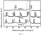
- this figure shows an in situ XRD of a tri-state phase transformation controlled by the method of regulating the gating voltage.
- a positive gating voltage an increasing rate of the voltage is 2 mV/s
- the (004) diffraction peak at 45.7° diminishes gradually and eventually disappears, while a diffraction peak corresponding to the new phase starts to develop at 44.0°, suggesting that the new structural phase SrCoO 2.5 H is obtained.
- the new phase SrCoO 2.5 H reverts back to SrCoO 2.5 quickly, when further increasing the negative gating voltage, SrCoO 2.5 H is transformed to a SrCoO 3- ⁇ phase having a perovskite structure.
- the structure transition can also be modulated reversibly by regulating the in situ electric field.
- SrCoO 3- ⁇ phase reverts back to SrCoO 2.5 phase and SrCoO 2.5 H quickly.
- SrCoO 2.5 , SrCoO 3- ⁇ , and SrCoO 2.5 H are shown.
- the SrCoO 2.5 phase having the brownmillerite structure exhibits a series of superstructure peaks derived from an alternating arrangement of oxygen octahedron and oxygen tetrahedron in an out-of-plane direction.
- Pseudo-cubic c-axis lattice constants of SrCoO 2.5 and SrCoO 3- ⁇ structures are respectively 0.397 nm and 0.381 nm based upon respective Bragg diffraction angles.
- the new phase SrCoO 2.5 H also has a series of superstructure diffraction peaks, suggesting that the SrCoO 2.5 H structure has a long range periodic lattice structure the same as the SrCoO 2.5 structure.
- the new phase SrCoO 2.5 H has a c-axis lattice constant of 0.411 nm which increases by 3.7% and 8.0% respectively compared to these of SrCoO 2.5 and SrCoO 3- ⁇ .
- a c-axis lattice constant of 0.411 nm which increases by 3.7% and 8.0% respectively compared to these of SrCoO 2.5 and SrCoO 3- ⁇ .
- films with different thicknesses (from 20 nm to 100 nm) grown on LSAT(001) and films with different stresses grown on STO(001) and LAO(001) substrates are provided, and similar results are obtained, which fully demonstrates the effectiveness and intrinsic nature of the reversible tri-state phase transformation among the three phases SrCoO 2.5 , SrCoO 3- ⁇ , and SrCoO 2.5 H. That is, this effect has no connection with a stress and a thickness or a dimension of a material and can be generalized to material systems of various structural forms.
- FIG. 9 a comparison of lattice volumes of the three structures obtained from XRD measurements with known bulk materials SrCoO 3 and SrCoO 2.5 is shown. It can be seen from FIG. 9 that the lattice volume of the first phase is greater than the lattice volume of the second phase, and the lattice volume of the second phase is greater than the lattice volume of the third phase.
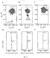
- the X-ray absorption spectroscopy at the L-absorption edge of Co and K-absorption edge of O in each of the three structure phases SrCoO 2.5 , SrCoO 3- ⁇ , and SrCoO 2.5 H is measured in order to thoroughly understand the electronic structure of the new phase SrCoO 2.5 H
- a transition of an electron of Co from 2p orbital to 3d orbital is detected at L 2,3 -absorption edge of Co and can be the basis for determining a valence state of corresponding compound.
- FIG. 10 the X-ray absorption spectroscopy at the L-absorption edge of Co and K-absorption edge of O in each of the three structure phases SrCoO 2.5 , SrCoO 3- ⁇ , and SrCoO 2.5 H is measured in order to thoroughly understand the electronic structure of the new phase SrCoO 2.5 H
- a transition of an electron of Co from 2p orbital to 3d orbital is detected at L 2,3 -absorption edge of Co and can be the basis for
- the peak position at 527.5 eV is significantly weaken and the peak position at 528.5 eV is significantly enhanced, suggesting a transformation thereof from a complete oxygen octahedral coordination to a partial oxygen octahedral and partial oxygen tetrahedral coordination.
- the adsorption peak at 528 eV completely disappeared, suggesting that the oxygen-cobalt hybridization has been suppressed to a great extent.
- FIG. 13 electrochromic real photos of the three phases and variation of energy gaps thereof are provided.
- FIG. 13a a material object comparison of transmittance among the three different phases SrCoO 2.5 , SrCoO 3- ⁇ , and SrCoO 2.5 H each having a thickness of 50 nm and grown on the LSAT(001) substrate is shown, in which SrCoO 2.5 H corresponds to the first phase, SrCoO 2.5 corresponds to the second phase, and SrCoO 3- ⁇ corresponds to the third phase. Sizes of transmittances of the three structural phases can be seen from FIG. 13a .
- FIG. 13b shows the direct bandgaps of the three structural phases.
- FIG. 14a a dual-band electrochromic effect possessed by the tri-state phase transformation is also shown clearly.
- the SrCoO 2.5 H phase (the first phase) has a transmittance over 30% greater than these of the other two phases in the visible light region, and the transmittance of the SrCoO 2.5 H phase (the first phase) and the SrCoO 2.5 phase (the second phase) are 60% greater than that of the SrCoO 3- ⁇ phase (the third phase) in the infrared region (the wavelength reaches 8000 nm).
- FIG. 14b shows differences in permeability and thermal effect (i.e. the principle of a smart glass) from a regulation to infrared and visible light bands.
- the SrCoO 2.5 H herein provides a great application prospect for the electrochromism, that is, an electric field regulation to a photopermeability can be performed selectively and independently at an infrared band and a visible light band by way of regulating a gate voltage. More specifically, when in the first phase (the SrCoO 2.5 H phase), for example, since the permeabilities of the infrared section and the visible light section are relatively high, it is achievable that more infrared rays and visible lights enter into a room at the same time, so that the temperature and the brightness are relatively high in the room.
- the tri-state phase transformation realized by the material broadens the application scope of the smart glass.
- FIG. 15 a comparison of absorption coefficients of optical absorption spectra obtained from the transmittance spectra of the three phases of the material of the embodiment of the present disclosure. It can be seen from the figure that when in an energy range below a photon energy of 4.0 eV, there are two main adsorption peaks, i.e. intraband d-d transition ( ⁇ , ⁇ , and ⁇ ) at the low energy end and interband p-d transition ( ⁇ , ⁇ , and ⁇ ) at the high energy end, in all three structural phases. SrCoO 3- ⁇ exhibits relatively strong light adsorption at the whole spectrum band, which is consistent with its metallic nature.
- SrCoO 2.5 and SrCoO 2.5 H both exhibit an insulation property and form very strong adsorptions ( ⁇ and ⁇ ) near the direct bandgaps.
- the light adsorption by the SrCoO 2.5 phase is even greater than that by the SrCoO 3- ⁇ phase at an energy range greater than the direct bandgap, owing to a larger p-d transition in the SrCoO 2.5 phase.
- the adsorption is strongly suppressed with the increase of the direct bandgap.
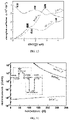
- FIG. 16 shows the dependences of resistivities of the three structure phases on the temperature, from which it can be seen that SrCoO 3- ⁇ is a good metal and has a resistivity of about 200 ⁇ •cm, and the SrCoO 2.5 phase and the SrCoO 2.5 H phase both show semiconductor behaviors and have resistivities of 8 ⁇ •cm and 450 ⁇ •cm respectively at room temperature.
- the inserted figure shows a reversible transformation among different resistance states among the three structural phases under the regulating of the electric field, i.e.
- the electric-field-controlled phase transformation among multi-resistance states realized by the present disclosure establishes a model device unit based on a resistance changing memory.
- a tri-state magnetoelectric coupling phenomenon closely associated with the structural transition is shown, that is, the magnetic property of the material can be regulated by an electric field so as to achieve a multi-states magnetic memory.
- the obtained saturation magnetic moment of the SrCoO 3- ⁇ phase is 2.4 ⁇ B /Co
- the Curie temperature of the SrCoO 3- ⁇ phase is 240 K
- SrCoO 2.5 only exhibits the intrinsic antiferromagnetic behavior of the material.
- the SrCoO 2.5 H phase also exhibits an obvious hysteresis loop, the saturation magnetic moment of the SrCoO 2.5 H phase is 0.6 ⁇ B /Co, and the Curie temperature of the SrCoO 2.5 H phase is 125 K.
- this figure illustrates a regulation among three electrical and magnetic states resulted from the insertion/extraction of the oxygen ion and the hydrogen ion controlled by the electric field, which provides a new tri-state magnetoelectric coupling mechanism with a potential application value for a next generation electron device the magnetic property of which is controlled by an electric field.
- this figure shows that a transformation among magnetic properties at different temperatures is achieved by controlling the phase transformation or the valence state of Co via the electric field.
- a ferromagnetic-antiferromagnetic-ferromagnetic transformation can be achieved at a temperature below 125 K; while a ferromagnetic-antiferromagnetic-paramagnetic transformation can be achieved between 125 k and 250 K; and a paramagnetic-antiferromagnetic-paramagnetic transformation can be achieved between 250 K and 537 K.
- a switch among different magnetic ground states at different temperatures can be achieved by a method of controlling a movement of ion or the phase transformation via the electric field, thereby greatly enriching a range and a content of an electric control of magnetism.
- a model of penta-state memory is established according to the magnetoelectric coupling and spin electronic effect on basis of the regulation to the magnetic ground states of the three phases.
- a spin-valve structure is established by using the three phases of SrCoO x H y having different spin ground states as a spin pinned layer and an epitaxial magnetic metal as a spin free layer.
- a high resistance state, a low resistance state-I, and a low resistance state-II can be achieved, wherein the low resistance states are each further distinguished into a high resistance state and a low resistance state, thereby realizing the penta-state memory finally.
- a phase transformation electron device 100 is further provided in combination with the hydrogen-containing transition metal oxide.
- the phase transformation electron device 100 can realize a mutual-reversible phase transformation among three phases under an action of an electric field. More specifically, the phase transformation electron device 100 can be an electrochromic smart glass, can be a multi-state resistance changing memory, and also can be a magnetic multi-state memory.
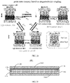
- the phase transformation electron device 100 includes a first conductive layer 120, a second conductive layer 140, an ionic liquid layer 130, and a phase transformation material layer 150. The ionic liquid layer 130 and the phase transformation material layer 150 are encapsulated between the first conductive layer 120 and the second conductive layer 140.
- the first conductive layer 120 is insulated from the second conductive layer 150 by an insulating support 170.
- the phase transformation material layer 150 is disposed on the second conductive layer 140.
- the phase transformation material layer 150 is formed by the hydrogen-containing transition metal oxide ABO x H y .
- the ionic liquid layer 130 is disposed between the phase transformation material layer 150 and the first conductive layer 120.
- a gating voltage can be applied to the ionic liquid layer 130 and the phase transformation material layer 150 via the first conductive layer 120 and the second conductive layer 140, and a tri-state phase transformation of the phase transformation material layer 150 can be achieved by controlling the gating voltage.
- the phase transformation material Under an action of an electric field, the phase transformation material is transformed among a first phase, a second phase, and a third phase.
- a lattice volume of the first phase is larger than a lattice volume of the second phase
- the lattice volume of the second phase is larger than a lattice volume of the third phase.
- the first phase is SrCoO 2.5 H
- the second phase is SrCoO 2.5
- the third phase is SrCoO 3- ⁇ .
- An electrochromism and a tri-state magnetoelectric coupling can be achieved.
- Materials of the first conductive layer 120 and the second conductive layer 140 are not limited and can be selected according to actual needs. For example, if the phase transformation electron device 100 is used for the electrochromism, then the first conductive layer 120 and the second conductive layer 140 can be disposed to be transparent conductive layers. It is to be understood that the phase transformation material layer 150 itself can be used directly as the second conductive layer 140 and the second conductive layer 140 can be omitted.
- a material of the insulating support 170 is not limited, as long as the material is insulative and has certain hardness.
- the insulating support 170 can be a glass or others.
- a material of the ionic liquid layer 130 is the first ionic liquid.
- the ionic liquid layer 130 is used for providing the hydrogen element and the oxygen element required for the phase transformation.
- the phase transformation electron device 100 further includes a first substrate 110 and a second substrate 160 opposite to and spaced from the first substrate 110.
- the first conductive layer 120 is disposed on a surface of the first substrate 110
- the second conductive layer 140 is disposed on a surface of the second substrate 160.
- the first substrate 110 and the second substrate 160 are used for supporting and can be made by a material with certain hardness.
- the first substrate 110 and the second substrate 160 are glasses.
Landscapes
- Physics & Mathematics (AREA)
- Chemical & Material Sciences (AREA)
- Nonlinear Science (AREA)
- Engineering & Computer Science (AREA)
- Inorganic Chemistry (AREA)
- General Physics & Mathematics (AREA)
- Optics & Photonics (AREA)
- Materials Engineering (AREA)
- Crystallography & Structural Chemistry (AREA)
- Manufacturing & Machinery (AREA)
- Electrochemistry (AREA)
- Chemical Kinetics & Catalysis (AREA)
- Electrochromic Elements, Electrophoresis, Or Variable Reflection Or Absorption Elements (AREA)
- Semiconductor Memories (AREA)
- Hall/Mr Elements (AREA)
- Mram Or Spin Memory Techniques (AREA)
- Optical Modulation, Optical Deflection, Nonlinear Optics, Optical Demodulation, Optical Logic Elements (AREA)
- Oxygen, Ozone, And Oxides In General (AREA)
- Inorganic Compounds Of Heavy Metals (AREA)
Claims (8)
- Verfahren zur Regulierung einer Phasenumwandlung eines wasserstoffhaltigen Übergangsmetalloxids, folgende Schritte umfassend:S100, Bereitstellen eines wasserstoffhaltigen Übergangsmetalloxids mit einer Strukturformel ABOxHy, wobei das wasserstoffhaltige Übergangsmetalloxid in Form einer ersten Phase vorliegt, A eines oder mehrere aus Erdalkalimetallelementen und Seltenerdmetallelementen ist, B eines oder mehrere aus Übergangsmetallelementen ist, x ein Zahlenwert in einem Bereich von 1 bis 3 ist und y ein Zahlenwert größer als 0 und kleiner als oder gleich 2,5 ist;S200, Tränken des wasserstoffhaltigen Übergangsmetalloxids mit einer ersten ionischen Flüssigkeit, die imstande ist, Wasserstoff-Ionen und Sauerstoff-Ionen zu liefern, undS300, Anlegen einer Gating-Spannung an das wasserstoffhaltige Übergangsmetalloxid über die erste ionische Flüssigkeit als Gate, um die Phasenumwandlung des wasserstoffhaltigen Übergangsmetalloxids zu regulieren;wobei das Verfahren zur Herstellung des wasserstoffhaltigen Übergangsmetalloxids folgende Schritte umfasst:S110, Bereitstellen eines Übergangsmetalloxids mit einer Strukturformel ABOz, wobei z größer als oder gleich 2 und kleiner als oder gleich 3 ist;S120, Tränken des Übergangsmetalloxids mit einer zweiten ionischen Flüssigkeit, wobei die zweite ionische Flüssigkeit imstande ist, durch Ionisierung von Wasser Wasserstoff-Ionen und Sauerstoff-Ionen zu liefern; undS130, Anlegen eines elektrischen Feldes an das Übergangsmetalloxid, um zu bewirken, dass die Wasserstoff-Ionen in der zweiten ionischen Flüssigkeit in das Übergangsmetalloxid eingebracht werden;dadurch gekennzeichnet, dass der Schritt S130 folgende Schritte umfasst:S132, Bereitstellen einer zweiten Elektrode und einer Stromquelle;S134, Anordnen der zweiten Elektrode beabstandet von der ersten Elektrode und Verbinden der zweiten Elektrode und der ersten Elektrode elektrisch und jeweils mit der Stromquelle; undS136, Tränken der zweiten Elektrode mit der zweiten ionischen Flüssigkeit und Anlegen eines elektrischen Feldes in einer Richtung von der zweiten Elektrode zu der ersten Elektrode mittels der Stromquelle.
- Verfahren zur Regulierung der Phasenumwandlung des wasserstoffhaltigen Übergangsmetalloxids nach Anspruch 1, dadurch gekennzeichnet, dass der Schritt S110 folgende Schritte umfasst:S112, Bereitstellen eines Substrates;S114, Abscheiden eines Films des Übergangsmetalloxids mit der Strukturformel ABOz auf eine Oberfläche des Substrates; undS116, Ausbilden einer ersten Elektrode auf einer Oberfläche des Films des Übergangsmetalloxids.
- Verfahren zur Regulierung der Phasenumwandlung des wasserstoffhaltigen Übergangsmetalloxids nach Anspruch 2, dadurch gekennzeichnet, dass das Substrat eines aus einem Keramiksubstrat, einem Siliciumsubstrat, einem Glassubstrat, einem Metallsubstrat oder einem Polymer ist und in dem Schritt S114 der Film des Übergangsmetalloxids durch epitaktisches Wachstum auf dem Substrat unter Anwendung eines Laserpulsabscheidungsverfahrens erhalten wird.
- Verfahren zur Regulierung der Phasenumwandlung des wasserstoffhaltigen Übergangsmetalloxids nach Anspruch 2, dadurch gekennzeichnet, dass in dem Schritt S116 die erste Elektrode mit dem Film des Übergangsmetalloxids in Kontakt steht, um eine untere Elektrode auszubilden.
- Verfahren zur Regulierung der Phasenumwandlung des wasserstoffhaltigen Übergangsmetalloxids nach Anspruch 1, dadurch gekennzeichnet, dass der Schritt S300 den folgenden Schritt umfasst:
S310, Anlegen einer negativen Gating-Spannung an das wasserstoffhaltige Übergangsmetalloxid ABOxHy, um die Wasserstoff-Ionen aus dem wasserstoffhaltigen Übergangsmetalloxid zu extrahieren oder die Sauerstoff-Ionen in das wasserstoffhaltige Übergangsmetalloxid einzubringen, um zu bewirken, dass das wasserstoffhaltige Übergangsmetalloxid in Form einer zweiten Phase vorliegt, wobei die zweite Phase ein Gittervolumen aufweist, das kleiner als das der ersten Phase ist. - Verfahren zur Regulierung der Phasenumwandlung des wasserstoffhaltigen Übergangsmetalloxids nach Anspruch 5, dadurch gekennzeichnet, dass der Schritt S300 einen folgenden Schritt umfasst:
S320, Anlegen einer positiven Gating-Spannung an das wasserstoffhaltige Übergangsmetalloxid in Form der zweiten Phase, um die Wasserstoff-Ionen in das wasserstoffhaltige Übergangsmetalloxid in Form der zweiten Phase einzubringen oder die Sauerstoff-Ionen aus diesem zu extrahieren, um zu bewirken, dass das wasserstoffhaltige Übergangsmetalloxid in Form der zweiten Phase in die erste Phase zurückkehrt. - Verfahren zur Regulierung der Phasenumwandlung des wasserstoffhaltigen Übergangsmetalloxids nach Anspruch 5, dadurch gekennzeichnet, dass der Schritt S300 den folgenden Schritt umfasst:
S330, Anlegen einer negativen Gating-Spannung an das wasserstoffhaltige Übergangsmetalloxid in Form der zweiten Phase, um die Sauerstoff-Ionen in das wasserstoffhaltige Übergangsmetalloxid in Form der zweiten Phase einzubringen oder die Wasserstoff-Ionen aus diesem zu extrahieren, damit dieses in Form einer dritten Phase vorliegt, wobei die dritte Phase ein Gittervolumen aufweist, das kleiner als das der zweiten Phase ist. - Verfahren zur Regulierung der Phasenumwandlung des wasserstoffhaltigen Übergangsmetalloxids nach Anspruch 1, dadurch gekennzeichnet, dass das ABOxHy SrCoO2.5H ist.
Applications Claiming Priority (2)
| Application Number | Priority Date | Filing Date | Title |
|---|---|---|---|
| CN201611056300.7A CN108091760B (zh) | 2016-11-23 | 2016-11-23 | 调控含氢过渡金属氧化物相变的方法 |
| PCT/CN2017/112611 WO2018095367A1 (zh) | 2016-11-23 | 2017-11-23 | 调控含氢过渡金属氧化物相变的方法 |
Publications (3)
| Publication Number | Publication Date |
|---|---|
| EP3547381A1 EP3547381A1 (de) | 2019-10-02 |
| EP3547381A4 EP3547381A4 (de) | 2019-12-25 |
| EP3547381B1 true EP3547381B1 (de) | 2022-05-11 |
Family
ID=62170251
Family Applications (1)
| Application Number | Title | Priority Date | Filing Date |
|---|---|---|---|
| EP17874222.7A Active EP3547381B1 (de) | 2016-11-23 | 2017-11-23 | Verfahren zur regulierung und steuerung des phasenwechsels eines wasserstoffhaltigen übergangsmetalloxids |
Country Status (5)
| Country | Link |
|---|---|
| US (1) | US11018294B2 (de) |
| EP (1) | EP3547381B1 (de) |
| JP (1) | JP6846066B2 (de) |
| CN (1) | CN108091760B (de) |
| WO (1) | WO2018095367A1 (de) |
Families Citing this family (3)
| Publication number | Priority date | Publication date | Assignee | Title |
|---|---|---|---|---|
| CN108091759B (zh) * | 2016-11-23 | 2019-07-09 | 清华大学 | 相变电子器件 |
| CN110580995B (zh) * | 2018-06-07 | 2020-11-13 | 清华大学 | 铁磁材料及其制备方法、传感器 |
| CN119592913B (zh) * | 2024-12-17 | 2025-09-02 | 季华实验室 | 一种窄滞回宽度薄膜材料及其制备方法、应用 |
Family Cites Families (28)
| Publication number | Priority date | Publication date | Assignee | Title |
|---|---|---|---|---|
| WO2000049659A1 (en) | 1999-02-17 | 2000-08-24 | International Business Machines Corporation | Microelectronic device for storing information and method thereof |
| US6964827B2 (en) | 2000-04-27 | 2005-11-15 | Valence Technology, Inc. | Alkali/transition metal halo- and hydroxy-phosphates and related electrode active materials |
| CN1199306C (zh) | 2001-01-21 | 2005-04-27 | 天津和平海湾电源集团有限公司 | 高能量空气/氢二次电池 |
| US7087186B1 (en) * | 2001-11-26 | 2006-08-08 | The United States Of America As Represented By The Secretary Of The Army | Ferroelectric/paraelectric materials, and phase shifter devices, true time delay devices and the like containing same |
| US6972238B2 (en) | 2003-05-21 | 2005-12-06 | Sharp Laboratories Of America, Inc. | Oxygen content system and method for controlling memory resistance properties |
| JP4534531B2 (ja) * | 2004-03-09 | 2010-09-01 | 株式会社豊田中央研究所 | 異方形状粉末の製造方法 |
| KR100612570B1 (ko) | 2004-04-21 | 2006-08-11 | 주식회사 엘지화학 | 신규 결정 구조를 갖는 금속 복합 산화물 및 이들의 이온전도체로서의 용도 |
| US7666550B2 (en) | 2004-05-25 | 2010-02-23 | Enerdel, Inc. | Lithium ion battery with oxidized polymer binder |
| JP4880894B2 (ja) | 2004-11-17 | 2012-02-22 | シャープ株式会社 | 半導体記憶装置の構造及びその製造方法 |
| JP4685507B2 (ja) * | 2005-05-19 | 2011-05-18 | 株式会社日立製作所 | エレクトロクロミックデバイス |
| JP2009519191A (ja) | 2005-08-09 | 2009-05-14 | ザ・ユニバーシティー・オブ・ヒューストン・システム | 固体状酸化物燃料電池/イオン輸送膜用の新規な陰極と電解質材料 |
| CN100469940C (zh) | 2005-09-15 | 2009-03-18 | 电子科技大学 | 金属氧化物薄膜的制备方法 |
| TWI340126B (en) | 2005-10-19 | 2011-04-11 | Lg Chemical Ltd | Composite oxides comprising strontium, lantanium, tungsten and ionic conductors using the same |
| CN100391589C (zh) * | 2006-07-11 | 2008-06-04 | 南开大学 | 镁-过渡金属氧化物复合储氢材料及其制备方法和应用 |
| US7479671B2 (en) * | 2006-08-29 | 2009-01-20 | International Business Machines Corporation | Thin film phase change memory cell formed on silicon-on-insulator substrate |
| JP2009054884A (ja) | 2007-08-28 | 2009-03-12 | Bridgestone Corp | キャパシタ用非水電解液及びそれを備えた非水電解液キャパシタ |
| JP5397668B2 (ja) | 2008-09-02 | 2014-01-22 | ソニー株式会社 | 記憶素子および記憶装置 |
| EP2349924B1 (de) | 2008-10-23 | 2017-02-08 | Centre National De La Recherche Scientifique | Fluorsulfate, die als elektrodenmaterialien verwendbar sind |
| CN101624206B (zh) | 2009-08-07 | 2010-12-08 | 南开大学 | 稀土金属氢氧化物或钒酸盐纳米材料的制备方法及应用 |
| JP2012182172A (ja) | 2011-02-28 | 2012-09-20 | Sony Corp | 記憶素子および記憶装置 |
| KR20140104840A (ko) | 2013-02-21 | 2014-08-29 | 삼성전자주식회사 | 산소이온전도성을 갖는 쉴라이트 구조 복합금속산화물 |
| US9590176B2 (en) * | 2013-03-14 | 2017-03-07 | International Business Machines Corporation | Controlling the conductivity of an oxide by applying voltage pulses to an ionic liquid |
| EP2793279A1 (de) | 2013-04-19 | 2014-10-22 | ETH Zurich | Gespannte mehrschichtige resistiv-schaltende Speicherelemente |
| JPWO2016063849A1 (ja) * | 2014-10-21 | 2017-08-10 | 旭硝子株式会社 | 光学素子および撮像装置 |
| EP3229281B1 (de) * | 2015-01-09 | 2020-08-19 | National University Corporation Hokkaido University | Schaltbauelement |
| JP6007994B2 (ja) * | 2015-01-23 | 2016-10-19 | セントラル硝子株式会社 | 非水電解液二次電池用電解液及びそれを用いた非水電解液二次電池 |
| CN104891448B (zh) * | 2015-05-19 | 2020-01-07 | 河北民族师范学院 | 一种过渡金属氧化物纳米材料、其制备方法及用途 |
| CN105047816A (zh) * | 2015-07-06 | 2015-11-11 | 中国科学院上海微系统与信息技术研究所 | 一种Cr掺杂Ge2Sb2Te5相变材料、相变存储器单元及其制备方法 |
-
2016
- 2016-11-23 CN CN201611056300.7A patent/CN108091760B/zh active Active
-
2017
- 2017-11-23 EP EP17874222.7A patent/EP3547381B1/de active Active
- 2017-11-23 WO PCT/CN2017/112611 patent/WO2018095367A1/zh not_active Ceased
- 2017-11-23 JP JP2019547752A patent/JP6846066B2/ja active Active
-
2019
- 2019-05-22 US US16/420,159 patent/US11018294B2/en active Active
Also Published As
| Publication number | Publication date |
|---|---|
| JP6846066B2 (ja) | 2021-03-24 |
| EP3547381A4 (de) | 2019-12-25 |
| US11018294B2 (en) | 2021-05-25 |
| JP2020501378A (ja) | 2020-01-16 |
| CN108091760B (zh) | 2019-11-22 |
| CN108091760A (zh) | 2018-05-29 |
| WO2018095367A1 (zh) | 2018-05-31 |
| EP3547381A1 (de) | 2019-10-02 |
| US20190280201A1 (en) | 2019-09-12 |
Similar Documents
| Publication | Publication Date | Title |
|---|---|---|
| US11434148B2 (en) | Hydrogen-containing transition metal oxide, method for making the same, and primary battery | |
| Yao et al. | Fabrication and resistive switching characteristics of high compact Ga-doped ZnO nanorod thin film devices | |
| Larbi et al. | Nickel content effect on the microstructural, optical and electrical properties of p-type Mn3O4 sprayed thin films | |
| Bouilly et al. | Electrical properties of epitaxial thin films of oxyhydrides ATiO3–x H x (A= Ba and Sr) | |
| US11018294B2 (en) | Method for regulating phase transformation of hydrogen-containing transition metal oxide | |
| US11502253B2 (en) | Phase transformation electronic device | |
| Sun et al. | Electrical properties and temperature sensitivity of Li/Mg modified Ni0. 7Zn0. 3O based ceramics | |
| EP3547431B1 (de) | Festoxidbrennstoffzelle und verfahren zur herstellung eines feststoffelektrolyten | |
| Wang et al. | Novel electrical conductivity properties in Ca-doped BiFeO3 nanoparticles | |
| EP3229281B1 (de) | Schaltbauelement | |
| McCloy et al. | Electrical and Magnetic Properties Modification in Heavy Ion Irradiated Nanograin Ni x Co (3–x) O4 Films | |
| Ezhilvalavan et al. | Dependence of non-linearity coefficients on transition metal oxide concentration in simplified compositions of ZnO+ Bi2O3+ MO varistor ceramics (M= Co or Mn) | |
| Boileau et al. | Inductive effect of Nd for Ni3+ stabilization in NdNiO3 synthesized by reactive DC cosputtering | |
| Megha et al. | Room temperature AC impedance and dielectric studies of Bi and Sr doped PrCo0. 6Fe0. 4O3 perovskites | |
| Tian et al. | Impedance spectroscopy and ferromagnetic properties of Bi0. 8Gd0. 2FeO3 multiferroics | |
| Mal et al. | Defect mediated reversible ferromagnetism in Co and Mn doped zinc oxide epitaxial films | |
| Radu et al. | Vanadium oxide as a memory material | |
| KR102532178B1 (ko) | 강상관전자계를 이용한 적외선 투과 전도체 및 그 제조방법 | |
| Yuan et al. | Ferromagnetic mechanism of (Co, Cu)-codoped ZnO films with different Co concentrations investigated by X-ray photoelectron spectroscopy | |
| Wang et al. | Effects of Co doping on electronic structure and electric/magnetic properties of La0. 1Bi0. 9FeO3 ceramics | |
| Abd et al. | Effect of annealing temperature on physical properties of indium doped cadmium oxide thin films | |
| CN110970549B (zh) | 含氢钌氧化物、电子器件及钌氧化物物性的调控方法 | |
| Kumari et al. | Magneto-dielectric anomaly in (Bi0. 95Nd0. 05)(Fe0. 97Mn0. 03) O3 electroceramic |
Legal Events
| Date | Code | Title | Description |
|---|---|---|---|
| STAA | Information on the status of an ep patent application or granted ep patent |
Free format text: STATUS: THE INTERNATIONAL PUBLICATION HAS BEEN MADE |
|
| PUAI | Public reference made under article 153(3) epc to a published international application that has entered the european phase |
Free format text: ORIGINAL CODE: 0009012 |
|
| STAA | Information on the status of an ep patent application or granted ep patent |
Free format text: STATUS: REQUEST FOR EXAMINATION WAS MADE |
|
| 17P | Request for examination filed |
Effective date: 20190618 |
|
| AK | Designated contracting states |
Kind code of ref document: A1 Designated state(s): AL AT BE BG CH CY CZ DE DK EE ES FI FR GB GR HR HU IE IS IT LI LT LU LV MC MK MT NL NO PL PT RO RS SE SI SK SM TR |
|
| AX | Request for extension of the european patent |
Extension state: BA ME |
|
| A4 | Supplementary search report drawn up and despatched |
Effective date: 20191126 |
|
| RIC1 | Information provided on ipc code assigned before grant |
Ipc: H01L 45/00 20060101AFI20191120BHEP Ipc: H01L 43/10 20060101ALI20191120BHEP Ipc: H01L 43/08 20060101ALI20191120BHEP |
|
| DAV | Request for validation of the european patent (deleted) | ||
| DAX | Request for extension of the european patent (deleted) | ||
| GRAP | Despatch of communication of intention to grant a patent |
Free format text: ORIGINAL CODE: EPIDOSNIGR1 |
|
| STAA | Information on the status of an ep patent application or granted ep patent |
Free format text: STATUS: GRANT OF PATENT IS INTENDED |
|
| INTG | Intention to grant announced |
Effective date: 20211216 |
|
| GRAS | Grant fee paid |
Free format text: ORIGINAL CODE: EPIDOSNIGR3 |
|
| GRAA | (expected) grant |
Free format text: ORIGINAL CODE: 0009210 |
|
| STAA | Information on the status of an ep patent application or granted ep patent |
Free format text: STATUS: THE PATENT HAS BEEN GRANTED |
|
| AK | Designated contracting states |
Kind code of ref document: B1 Designated state(s): AL AT BE BG CH CY CZ DE DK EE ES FI FR GB GR HR HU IE IS IT LI LT LU LV MC MK MT NL NO PL PT RO RS SE SI SK SM TR |
|
| REG | Reference to a national code |
Ref country code: GB Ref legal event code: FG4D |
|
| REG | Reference to a national code |
Ref country code: CH Ref legal event code: EP |
|
| REG | Reference to a national code |
Ref country code: AT Ref legal event code: REF Ref document number: 1492217 Country of ref document: AT Kind code of ref document: T Effective date: 20220515 |
|
| REG | Reference to a national code |
Ref country code: DE Ref legal event code: R096 Ref document number: 602017057470 Country of ref document: DE |
|
| REG | Reference to a national code |
Ref country code: IE Ref legal event code: FG4D |
|
| REG | Reference to a national code |
Ref country code: LT Ref legal event code: MG9D |
|
| REG | Reference to a national code |
Ref country code: NL Ref legal event code: MP Effective date: 20220511 |
|
| REG | Reference to a national code |
Ref country code: AT Ref legal event code: MK05 Ref document number: 1492217 Country of ref document: AT Kind code of ref document: T Effective date: 20220511 |
|
| PG25 | Lapsed in a contracting state [announced via postgrant information from national office to epo] |
Ref country code: SE Free format text: LAPSE BECAUSE OF FAILURE TO SUBMIT A TRANSLATION OF THE DESCRIPTION OR TO PAY THE FEE WITHIN THE PRESCRIBED TIME-LIMIT Effective date: 20220511 Ref country code: PT Free format text: LAPSE BECAUSE OF FAILURE TO SUBMIT A TRANSLATION OF THE DESCRIPTION OR TO PAY THE FEE WITHIN THE PRESCRIBED TIME-LIMIT Effective date: 20220912 Ref country code: NO Free format text: LAPSE BECAUSE OF FAILURE TO SUBMIT A TRANSLATION OF THE DESCRIPTION OR TO PAY THE FEE WITHIN THE PRESCRIBED TIME-LIMIT Effective date: 20220811 Ref country code: NL Free format text: LAPSE BECAUSE OF FAILURE TO SUBMIT A TRANSLATION OF THE DESCRIPTION OR TO PAY THE FEE WITHIN THE PRESCRIBED TIME-LIMIT Effective date: 20220511 Ref country code: LT Free format text: LAPSE BECAUSE OF FAILURE TO SUBMIT A TRANSLATION OF THE DESCRIPTION OR TO PAY THE FEE WITHIN THE PRESCRIBED TIME-LIMIT Effective date: 20220511 Ref country code: HR Free format text: LAPSE BECAUSE OF FAILURE TO SUBMIT A TRANSLATION OF THE DESCRIPTION OR TO PAY THE FEE WITHIN THE PRESCRIBED TIME-LIMIT Effective date: 20220511 Ref country code: GR Free format text: LAPSE BECAUSE OF FAILURE TO SUBMIT A TRANSLATION OF THE DESCRIPTION OR TO PAY THE FEE WITHIN THE PRESCRIBED TIME-LIMIT Effective date: 20220812 Ref country code: FI Free format text: LAPSE BECAUSE OF FAILURE TO SUBMIT A TRANSLATION OF THE DESCRIPTION OR TO PAY THE FEE WITHIN THE PRESCRIBED TIME-LIMIT Effective date: 20220511 Ref country code: ES Free format text: LAPSE BECAUSE OF FAILURE TO SUBMIT A TRANSLATION OF THE DESCRIPTION OR TO PAY THE FEE WITHIN THE PRESCRIBED TIME-LIMIT Effective date: 20220511 Ref country code: BG Free format text: LAPSE BECAUSE OF FAILURE TO SUBMIT A TRANSLATION OF THE DESCRIPTION OR TO PAY THE FEE WITHIN THE PRESCRIBED TIME-LIMIT Effective date: 20220811 Ref country code: AT Free format text: LAPSE BECAUSE OF FAILURE TO SUBMIT A TRANSLATION OF THE DESCRIPTION OR TO PAY THE FEE WITHIN THE PRESCRIBED TIME-LIMIT Effective date: 20220511 |
|
| REG | Reference to a national code |
Ref country code: DE Ref legal event code: R079 Ref document number: 602017057470 Country of ref document: DE Free format text: PREVIOUS MAIN CLASS: H01L0045000000 Ipc: H10N0070000000 |
|
| PG25 | Lapsed in a contracting state [announced via postgrant information from national office to epo] |
Ref country code: RS Free format text: LAPSE BECAUSE OF FAILURE TO SUBMIT A TRANSLATION OF THE DESCRIPTION OR TO PAY THE FEE WITHIN THE PRESCRIBED TIME-LIMIT Effective date: 20220511 Ref country code: PL Free format text: LAPSE BECAUSE OF FAILURE TO SUBMIT A TRANSLATION OF THE DESCRIPTION OR TO PAY THE FEE WITHIN THE PRESCRIBED TIME-LIMIT Effective date: 20220511 Ref country code: LV Free format text: LAPSE BECAUSE OF FAILURE TO SUBMIT A TRANSLATION OF THE DESCRIPTION OR TO PAY THE FEE WITHIN THE PRESCRIBED TIME-LIMIT Effective date: 20220511 Ref country code: IS Free format text: LAPSE BECAUSE OF FAILURE TO SUBMIT A TRANSLATION OF THE DESCRIPTION OR TO PAY THE FEE WITHIN THE PRESCRIBED TIME-LIMIT Effective date: 20220911 |
|
| PG25 | Lapsed in a contracting state [announced via postgrant information from national office to epo] |
Ref country code: SM Free format text: LAPSE BECAUSE OF FAILURE TO SUBMIT A TRANSLATION OF THE DESCRIPTION OR TO PAY THE FEE WITHIN THE PRESCRIBED TIME-LIMIT Effective date: 20220511 Ref country code: SK Free format text: LAPSE BECAUSE OF FAILURE TO SUBMIT A TRANSLATION OF THE DESCRIPTION OR TO PAY THE FEE WITHIN THE PRESCRIBED TIME-LIMIT Effective date: 20220511 Ref country code: RO Free format text: LAPSE BECAUSE OF FAILURE TO SUBMIT A TRANSLATION OF THE DESCRIPTION OR TO PAY THE FEE WITHIN THE PRESCRIBED TIME-LIMIT Effective date: 20220511 Ref country code: EE Free format text: LAPSE BECAUSE OF FAILURE TO SUBMIT A TRANSLATION OF THE DESCRIPTION OR TO PAY THE FEE WITHIN THE PRESCRIBED TIME-LIMIT Effective date: 20220511 Ref country code: DK Free format text: LAPSE BECAUSE OF FAILURE TO SUBMIT A TRANSLATION OF THE DESCRIPTION OR TO PAY THE FEE WITHIN THE PRESCRIBED TIME-LIMIT Effective date: 20220511 Ref country code: CZ Free format text: LAPSE BECAUSE OF FAILURE TO SUBMIT A TRANSLATION OF THE DESCRIPTION OR TO PAY THE FEE WITHIN THE PRESCRIBED TIME-LIMIT Effective date: 20220511 |
|
| REG | Reference to a national code |
Ref country code: DE Ref legal event code: R097 Ref document number: 602017057470 Country of ref document: DE |
|
| PLBE | No opposition filed within time limit |
Free format text: ORIGINAL CODE: 0009261 |
|
| STAA | Information on the status of an ep patent application or granted ep patent |
Free format text: STATUS: NO OPPOSITION FILED WITHIN TIME LIMIT |
|
| PG25 | Lapsed in a contracting state [announced via postgrant information from national office to epo] |
Ref country code: AL Free format text: LAPSE BECAUSE OF FAILURE TO SUBMIT A TRANSLATION OF THE DESCRIPTION OR TO PAY THE FEE WITHIN THE PRESCRIBED TIME-LIMIT Effective date: 20220511 |
|
| 26N | No opposition filed |
Effective date: 20230214 |
|
| PG25 | Lapsed in a contracting state [announced via postgrant information from national office to epo] |
Ref country code: SI Free format text: LAPSE BECAUSE OF FAILURE TO SUBMIT A TRANSLATION OF THE DESCRIPTION OR TO PAY THE FEE WITHIN THE PRESCRIBED TIME-LIMIT Effective date: 20220511 |
|
| PG25 | Lapsed in a contracting state [announced via postgrant information from national office to epo] |
Ref country code: MC Free format text: LAPSE BECAUSE OF FAILURE TO SUBMIT A TRANSLATION OF THE DESCRIPTION OR TO PAY THE FEE WITHIN THE PRESCRIBED TIME-LIMIT Effective date: 20220511 |
|
| REG | Reference to a national code |
Ref country code: CH Ref legal event code: PL |
|
| REG | Reference to a national code |
Ref country code: BE Ref legal event code: MM Effective date: 20221130 |
|
| PG25 | Lapsed in a contracting state [announced via postgrant information from national office to epo] |
Ref country code: LI Free format text: LAPSE BECAUSE OF NON-PAYMENT OF DUE FEES Effective date: 20221130 Ref country code: CH Free format text: LAPSE BECAUSE OF NON-PAYMENT OF DUE FEES Effective date: 20221130 |
|
| PG25 | Lapsed in a contracting state [announced via postgrant information from national office to epo] |
Ref country code: LU Free format text: LAPSE BECAUSE OF NON-PAYMENT OF DUE FEES Effective date: 20221123 |
|
| PG25 | Lapsed in a contracting state [announced via postgrant information from national office to epo] |
Ref country code: IE Free format text: LAPSE BECAUSE OF NON-PAYMENT OF DUE FEES Effective date: 20221123 |
|
| PG25 | Lapsed in a contracting state [announced via postgrant information from national office to epo] |
Ref country code: BE Free format text: LAPSE BECAUSE OF NON-PAYMENT OF DUE FEES Effective date: 20221130 |
|
| PG25 | Lapsed in a contracting state [announced via postgrant information from national office to epo] |
Ref country code: IT Free format text: LAPSE BECAUSE OF FAILURE TO SUBMIT A TRANSLATION OF THE DESCRIPTION OR TO PAY THE FEE WITHIN THE PRESCRIBED TIME-LIMIT Effective date: 20220511 |
|
| PG25 | Lapsed in a contracting state [announced via postgrant information from national office to epo] |
Ref country code: HU Free format text: LAPSE BECAUSE OF FAILURE TO SUBMIT A TRANSLATION OF THE DESCRIPTION OR TO PAY THE FEE WITHIN THE PRESCRIBED TIME-LIMIT; INVALID AB INITIO Effective date: 20171123 |
|
| PG25 | Lapsed in a contracting state [announced via postgrant information from national office to epo] |
Ref country code: CY Free format text: LAPSE BECAUSE OF FAILURE TO SUBMIT A TRANSLATION OF THE DESCRIPTION OR TO PAY THE FEE WITHIN THE PRESCRIBED TIME-LIMIT Effective date: 20220511 |
|
| PG25 | Lapsed in a contracting state [announced via postgrant information from national office to epo] |
Ref country code: MK Free format text: LAPSE BECAUSE OF FAILURE TO SUBMIT A TRANSLATION OF THE DESCRIPTION OR TO PAY THE FEE WITHIN THE PRESCRIBED TIME-LIMIT Effective date: 20220511 |
|
| PG25 | Lapsed in a contracting state [announced via postgrant information from national office to epo] |
Ref country code: MT Free format text: LAPSE BECAUSE OF FAILURE TO SUBMIT A TRANSLATION OF THE DESCRIPTION OR TO PAY THE FEE WITHIN THE PRESCRIBED TIME-LIMIT Effective date: 20220511 |
|
| PG25 | Lapsed in a contracting state [announced via postgrant information from national office to epo] |
Ref country code: BG Free format text: LAPSE BECAUSE OF FAILURE TO SUBMIT A TRANSLATION OF THE DESCRIPTION OR TO PAY THE FEE WITHIN THE PRESCRIBED TIME-LIMIT Effective date: 20220511 |
|
| PG25 | Lapsed in a contracting state [announced via postgrant information from national office to epo] |
Ref country code: BG Free format text: LAPSE BECAUSE OF FAILURE TO SUBMIT A TRANSLATION OF THE DESCRIPTION OR TO PAY THE FEE WITHIN THE PRESCRIBED TIME-LIMIT Effective date: 20220511 |
|
| PG25 | Lapsed in a contracting state [announced via postgrant information from national office to epo] |
Ref country code: TR Free format text: LAPSE BECAUSE OF FAILURE TO SUBMIT A TRANSLATION OF THE DESCRIPTION OR TO PAY THE FEE WITHIN THE PRESCRIBED TIME-LIMIT Effective date: 20220511 |
|
| PGFP | Annual fee paid to national office [announced via postgrant information from national office to epo] |
Ref country code: DE Payment date: 20251127 Year of fee payment: 9 |
|
| PGFP | Annual fee paid to national office [announced via postgrant information from national office to epo] |
Ref country code: GB Payment date: 20251124 Year of fee payment: 9 |
|
| PGFP | Annual fee paid to national office [announced via postgrant information from national office to epo] |
Ref country code: FR Payment date: 20251124 Year of fee payment: 9 |