EP3537477A2 - Halbleiterbauelement und verfahren zur herstellung eines halbleiterbauelements - Google Patents
Halbleiterbauelement und verfahren zur herstellung eines halbleiterbauelements Download PDFInfo
- Publication number
- EP3537477A2 EP3537477A2 EP19155607.5A EP19155607A EP3537477A2 EP 3537477 A2 EP3537477 A2 EP 3537477A2 EP 19155607 A EP19155607 A EP 19155607A EP 3537477 A2 EP3537477 A2 EP 3537477A2
- Authority
- EP
- European Patent Office
- Prior art keywords
- conductive film
- cut surface
- gate portion
- semiconductor device
- region
- Prior art date
- Legal status (The legal status is an assumption and is not a legal conclusion. Google has not performed a legal analysis and makes no representation as to the accuracy of the status listed.)
- Withdrawn
Links
Images





Classifications
-
- H—ELECTRICITY
- H10—SEMICONDUCTOR DEVICES; ELECTRIC SOLID-STATE DEVICES NOT OTHERWISE PROVIDED FOR
- H10D—INORGANIC ELECTRIC SEMICONDUCTOR DEVICES
- H10D64/00—Electrodes of devices having potential barriers
- H10D64/60—Electrodes characterised by their materials
- H10D64/66—Electrodes having a conductor capacitively coupled to a semiconductor by an insulator, e.g. MIS electrodes
- H10D64/68—Electrodes having a conductor capacitively coupled to a semiconductor by an insulator, e.g. MIS electrodes characterised by the insulator, e.g. by the gate insulator
- H10D64/681—Electrodes having a conductor capacitively coupled to a semiconductor by an insulator, e.g. MIS electrodes characterised by the insulator, e.g. by the gate insulator having a compositional variation, e.g. multilayered
-
- H—ELECTRICITY
- H10—SEMICONDUCTOR DEVICES; ELECTRIC SOLID-STATE DEVICES NOT OTHERWISE PROVIDED FOR
- H10D—INORGANIC ELECTRIC SEMICONDUCTOR DEVICES
- H10D30/00—Field-effect transistors [FET]
- H10D30/60—Insulated-gate field-effect transistors [IGFET]
- H10D30/69—IGFETs having charge trapping gate insulators, e.g. MNOS transistors
- H10D30/694—IGFETs having charge trapping gate insulators, e.g. MNOS transistors characterised by the shapes, relative sizes or dispositions of the gate electrodes
- H10D30/696—IGFETs having charge trapping gate insulators, e.g. MNOS transistors characterised by the shapes, relative sizes or dispositions of the gate electrodes having at least one additional gate, e.g. program gate, erase gate or select gate
-
- H—ELECTRICITY
- H10—SEMICONDUCTOR DEVICES; ELECTRIC SOLID-STATE DEVICES NOT OTHERWISE PROVIDED FOR
- H10B—ELECTRONIC MEMORY DEVICES
- H10B43/00—EEPROM devices comprising charge-trapping gate insulators
- H10B43/10—EEPROM devices comprising charge-trapping gate insulators characterised by the top-view layout
-
- H—ELECTRICITY
- H10—SEMICONDUCTOR DEVICES; ELECTRIC SOLID-STATE DEVICES NOT OTHERWISE PROVIDED FOR
- H10B—ELECTRONIC MEMORY DEVICES
- H10B43/00—EEPROM devices comprising charge-trapping gate insulators
- H10B43/30—EEPROM devices comprising charge-trapping gate insulators characterised by the memory core region
-
- H—ELECTRICITY
- H10—SEMICONDUCTOR DEVICES; ELECTRIC SOLID-STATE DEVICES NOT OTHERWISE PROVIDED FOR
- H10B—ELECTRONIC MEMORY DEVICES
- H10B43/00—EEPROM devices comprising charge-trapping gate insulators
- H10B43/40—EEPROM devices comprising charge-trapping gate insulators characterised by the peripheral circuit region
-
- H—ELECTRICITY
- H10—SEMICONDUCTOR DEVICES; ELECTRIC SOLID-STATE DEVICES NOT OTHERWISE PROVIDED FOR
- H10D—INORGANIC ELECTRIC SEMICONDUCTOR DEVICES
- H10D30/00—Field-effect transistors [FET]
- H10D30/01—Manufacture or treatment
- H10D30/021—Manufacture or treatment of FETs having insulated gates [IGFET]
- H10D30/0413—Manufacture or treatment of FETs having insulated gates [IGFET] of FETs having charge-trapping gate insulators, e.g. MNOS transistors
-
- H—ELECTRICITY
- H10—SEMICONDUCTOR DEVICES; ELECTRIC SOLID-STATE DEVICES NOT OTHERWISE PROVIDED FOR
- H10D—INORGANIC ELECTRIC SEMICONDUCTOR DEVICES
- H10D30/00—Field-effect transistors [FET]
- H10D30/60—Insulated-gate field-effect transistors [IGFET]
- H10D30/69—IGFETs having charge trapping gate insulators, e.g. MNOS transistors
-
- H—ELECTRICITY
- H10—SEMICONDUCTOR DEVICES; ELECTRIC SOLID-STATE DEVICES NOT OTHERWISE PROVIDED FOR
- H10D—INORGANIC ELECTRIC SEMICONDUCTOR DEVICES
- H10D64/00—Electrodes of devices having potential barriers
- H10D64/01—Manufacture or treatment
- H10D64/011—Manufacture or treatment of electrodes ohmically coupled to a semiconductor
-
- H—ELECTRICITY
- H10—SEMICONDUCTOR DEVICES; ELECTRIC SOLID-STATE DEVICES NOT OTHERWISE PROVIDED FOR
- H10D—INORGANIC ELECTRIC SEMICONDUCTOR DEVICES
- H10D64/00—Electrodes of devices having potential barriers
- H10D64/01—Manufacture or treatment
- H10D64/013—Manufacture or treatment of electrodes having a conductor capacitively coupled to a semiconductor by an insulator
- H10D64/01302—Manufacture or treatment of electrodes having a conductor capacitively coupled to a semiconductor by an insulator the insulator being formed after the semiconductor body, the semiconductor being silicon
- H10D64/01332—Making the insulator
-
- H—ELECTRICITY
- H10—SEMICONDUCTOR DEVICES; ELECTRIC SOLID-STATE DEVICES NOT OTHERWISE PROVIDED FOR
- H10D—INORGANIC ELECTRIC SEMICONDUCTOR DEVICES
- H10D64/00—Electrodes of devices having potential barriers
- H10D64/01—Manufacture or treatment
- H10D64/031—Manufacture or treatment of data-storage electrodes
- H10D64/037—Manufacture or treatment of data-storage electrodes comprising charge-trapping insulators
-
- H—ELECTRICITY
- H10—SEMICONDUCTOR DEVICES; ELECTRIC SOLID-STATE DEVICES NOT OTHERWISE PROVIDED FOR
- H10D—INORGANIC ELECTRIC SEMICONDUCTOR DEVICES
- H10D64/00—Electrodes of devices having potential barriers
- H10D64/20—Electrodes characterised by their shapes, relative sizes or dispositions
- H10D64/27—Electrodes not carrying the current to be rectified, amplified, oscillated or switched, e.g. gates
-
- H—ELECTRICITY
- H10—SEMICONDUCTOR DEVICES; ELECTRIC SOLID-STATE DEVICES NOT OTHERWISE PROVIDED FOR
- H10D—INORGANIC ELECTRIC SEMICONDUCTOR DEVICES
- H10D64/00—Electrodes of devices having potential barriers
- H10D64/60—Electrodes characterised by their materials
- H10D64/66—Electrodes having a conductor capacitively coupled to a semiconductor by an insulator, e.g. MIS electrodes
- H10D64/68—Electrodes having a conductor capacitively coupled to a semiconductor by an insulator, e.g. MIS electrodes characterised by the insulator, e.g. by the gate insulator
Definitions
- the present invention relates to a semiconductor device and a manufacturing method of the semiconductor device.
- Patent Document 1 Japanese Unexamined Patent Application Publication No. 2015-103698
- the semiconductor device described therein has a semiconductor substrate including a main surface, and a memory gate electrode portion and a control gate electrode portion arranged over the main surface of the semiconductor substrate.
- the side wall of the memory gate electrode portion and that of the control gate electrode portion are insulated from each other.
- the memory gate electrode portion has a first portion and a second portion.
- the first portion and the second portion extend along a Y direction in a plane parallel to the main surface of the semiconductor substrate.
- the first portion and the second portion are in a plane parallel to the main surface of the semiconductor substrate and are arranged to be spaced apart from each other in an X direction perpendicular to the Y direction.
- the control gate electrode portion has a third portion and a fourth portion.
- the third portion and the fourth portion extend along the Y direction.
- the third portion is arranged adjacent to the first portion in the X direction.
- the fourth portion is arranged adjacent to the second portion in the X direction.
- the first portion and the second portion are arranged between the third portion and the fourth portion.
- the material configuring the control gate electrode portion is firstly formed over the main surface of the semiconductor substrate. Secondly, the material configuring the formed control gate electrode portion is patterned. Thirdly, the material configuring the memory gate electrode portion is formed to cover the material configuring the patterned control gate electrode portion. Fourthly, the material configuring the formed memory gate electrode portion is patterned by etch-back. Fifthly, the material configuring the patterned control gate electrode portion and material configuring the memory gate electrode portion are cut by etching so as to be spaced apart from each other in the X direction.
- Patent Document 1 Japanese Unexamined Patent Application Publication No. 2015-103698
- a semiconductor device includes: a semiconductor substrate having a first surface; a first conductive film that is located over the first surface and is formed to circle in plan view; a second conductive film that is located over the first surface and surrounds the outer periphery of the first conductive film in plan view; a first insulating spacer located between the first conductive film and the second conductive film; a first gate insulating film that is located between the first surface and the first conductive film and the accumulated amount of charges of which changes due to a change in the voltage between the first conductive film and the semiconductor substrate; and a second gate insulating film located between the first surface and the second conductive film.
- the first conductive film has a first memory gate portion and a second memory gate portion. In plan view, the first memory gate portion and the second memory gate portion are spaced apart from each other in a first direction, and extend along a second direction perpendicular to the first direction.
- the second conductive film has a first control gate portion extending along the first memory gate portion and a second control gate portion extending along the second memory gate portion.
- the semiconductor substrate has a first drain region located in the first surface, a source region located in the first surface, and a second drain region located in the first surface.
- the first memory gate portion and the first control gate portion are sandwiched by the first drain region and the source region in plan view.
- the second memory gate portion and the second control gate portion are sandwiched by the second drain region and the source region in plan view.
- the semiconductor device has a memory portion MB and a logic portion LOG, as illustrated in Fig. 1 .
- the memory portion MB includes a memory cell array MCA.
- the memory portion MB includes, in addition to the memory cell array MCA, a control circuit, an input/output circuit, an address buffer circuit, a row address decoder circuit, a column address decoder circuit, a sense amplifier circuit, a power supply circuit, and the like.
- the logic portion LOG includes a logic circuit including, for example, a CMOS (Complementary Metal Oxide Semiconductor) circuit.
- the memory portion MB and the logic portion LOG are formed in a semiconductor substrate SUB.
- the semiconductor substrate SUB has a first surface FS and a second surface SS (see Fig. 3 ).
- the second surface SS is a surface opposite to the first surface FS.
- the first surface FS and the second surface SS configure the main surfaces of the semiconductor substrate SUB.
- the semiconductor substrate SUB is formed of, for example, a single crystal of silicon (Si).
- the first conductive film CF1 is formed of, for example, polycrystalline silicon doped with impurities.
- the first conductive film CF1 is arranged over the first surface FS.
- the first conductive film CF1 has a first coupling portion CF1a, a first memory gate portion CF1b, a second memory gate portion CF1c, and a second coupling portion CF1d.
- the first coupling portion CF1a extends along a first direction DR1 in plan view (viewed from a direction perpendicular to the first surface FS).
- the first coupling portion CF1a has a first end and a second end in the first direction DR1.
- the first end is one end, in the first direction DR1, of the first coupling portion CF1a.
- the second end is the end opposite to the first end, in the first direction DR1, of the first coupling portion CF1a.
- the first memory gate portion CF1b extends along a second direction DR2 perpendicular to the first direction DR1 in plan view.
- the first memory gate portion CF1b extends from the first end of the first coupling portion CF1a.
- the second memory gate portion CF1c extends along the second direction DR2.
- the second memory gate portion CF1c extends from the second end of the first coupling portion CF1a. That is, the first memory gate portion CF1b and the second memory gate portion CF1c are spaced apart from each other in the first direction DR1.
- the second coupling portion CF1d couples the end of the first memory gate portion CF1b, opposite to the end on the first coupling portion CF1a side, and the end of the second memory gate portion CF1c, opposite to the end on the first coupling portion CF1a side. That is, the first conductive film CF1 is formed to circle in plan view. From another point of view, this means that the first conductive film CF1 is not cut in the middle.
- the second coupling portion CF1d extends along the first direction DR1.
- the second conductive film CF2 is formed of, for example, polycrystalline silicon doped with impurities.
- the second conductive film CF2 is arranged over the first surface FS.
- the second conductive film CF2 surrounds the outer periphery of the first conductive film CF1 in plan view.
- the second conductive film CF2 has a third coupling portion CF2a, a first control gate portion CF2b, a second control gate portion CF2c, and a fourth coupling portion CF2d.
- the third coupling portion CF2a extends along the first direction DR1.
- the third coupling portion CF2a has a third end and a fourth end in the first direction DR1.
- the third end is one end, in the first direction DR1, of the third coupling portion CF2a.
- the fourth end is the end of the third coupling portion CF2a, opposite to the third end in the first direction DR1.
- the third coupling portion CF2a extends along the first coupling portion CF1a.
- the first control gate portion CF2b extends along the second direction DR2.
- the first control gate portion CF2b extends from the third end of the third coupling portion CF2a.
- the first control gate portion CF2b extends along the first memory gate portion CF1b.
- the second control gate portion CF2c extends along the second direction DR2.
- the second control gate portion CF2c extends from the fourth end of the third coupling portion CF2a.
- the second control gate portion CF2c extends along the second memory gate portion CF1c.
- the fourth coupling portion CF2d couples the end of the first control gate portion CF2b, opposite to the end on the third coupling portion CF2a side, and the end of the second control gate portion CF2c, opposite to the end on the third coupling portion CF2a side. That is, the second conductive film CF2 is not cut in the middle.
- the fourth coupling portion CF2d extends along the first direction DR1.
- the insulating spacer ISS1 includes an insulator.
- silicon oxide (SiO 2 ), silicon nitride (SiN), or the like is used for the insulating spacer ISS1.
- the insulating spacer ISS1 is located between the first conductive film CF1 and the second conductive film CF2 in plan view. More specifically, the insulating spacer ISS1 is arranged between the side wall on the outer peripheral side of the first conductive film CF1 and the side wall on the inner peripheral side of the second conductive film CF2.
- the first drain region DRA1, the source region SR, and the second drain region DRA2 are arranged in the first surface FS.
- the first drain region DRA1, the source region SR, and the second drain region DRA2 are arranged to be spaced apart from each other in the first direction DR1.
- the well region WR is arranged in the first surface FS so as to surround the first drain region DRA1, the source region SR, and the second drain region DRA2.
- the first drain region DRA1 is arranged to sandwich, in the first direction DR1, the first memory gate portion CF1b and the first control gate portion CF2b with the source region SR.
- the second drain region DRA2 is arranged to sandwich, in the first direction DR1, the second memory gate portion CF1c and the second control gate portion CF2c with the source region SR.
- the first gate insulating film GIF1 is located between the first conductive film CF1 and the first surface FS. As the voltage between the first conductive film CF1 and the semiconductor substrate SUB changes, the accumulated amount of charges in the first gate insulating film GIF1 changes.
- the first gate insulating film GIF1 is preferably thicker than the second gate insulating film GIF2.
- the third layer is arranged over the second layer.
- the third layer includes hafnium silicate (HfSiO).
- the fourth layer is arranged over the third layer.
- the fourth layer includes aluminum oxide. That is, the first gate insulating film GIF1 may be an AHAO (Aluminum Hafnium Aluminum Oxide) film.
- the first gate insulating film GIF1 is not limited to an AHAO film.
- the first gate insulating film GIF1 may include, for example, an ONO (Oxide Nitride Oxide) film including a first silicon oxide film arranged directly over the first surface FS, a silicon nitride film arranged over the first silicon oxide film, and a second silicon oxide film arranged over the silicon nitride film.
- ONO Oxide Nitride Oxide
- the second gate insulating film GIF2 includes, for example, silicon oxide.
- the second gate insulating film GIF2 is arranged between the first surface FS and the second conductive film CF2.
- the first drain region DRA1, the source region SR, the well region WR, the first gate insulating film GIF1, the second gate insulating film GIF2, the first memory gate portion CF1b, and the first control gate portion CF2b configure a split gate type flash memory cell MC1.
- the second drain region DRA2, the source region SR, the well region WR, the first gate insulating film GIF1, the second gate insulating film GIF2, the second memory gate portion CF1c, and the second control gate portion CF2c configure a split gate type flash memory cell MC2.
- the semiconductor device according to First Embodiment further includes a hard mask HM.
- the hard mask HM includes an insulator.
- silicon oxide or silicon nitride is used for the hard mask HM.
- the hard mask HM is arranged over the upper surface of the first conductive film CF1.
- the semiconductor device further includes an interlayer insulating film ILD1, an interlayer insulating film ILD2, a contact plug CP1, a contact plug CP2, a contact plug CP3, a contact plug CP4, a contact plug CP5, a contact plug CP6, a contact plug CP7, wiring WL1a, wiring WL1b, wiring WL1c, wiring WL2a (first bit line), and wiring WL2b (second bit line).
- the interlayer insulating film ILD1 is arranged over the first surface FS.
- the interlayer insulating film ILD1 includes, for example, silicon oxide.
- a contact hole CH is provided in the interlayer insulating film ILD1. The contact hole CH penetrates through the interlayer insulating film ILD1 in the thickness direction.
- the contact plug CP1 to the contact plug CP7 include, for example, tungsten (W) or the like.
- the contact plug CP1 to the contact plug CP7 are arranged in the interlayer insulating film ILD1. More specifically, each of the contact plug CP1 to the contact plug CP7 is buried in the contact hole CH.
- a distance DIS1 between the contact plug CP1 (contact plug CP2) and one end, in the second direction DR2, of the first coupling portion CF1a (second coupling portion CF1d) is larger than a distance DIS2 between the contact plug CP1 (contact plug CP2) and the other end, in the second direction DR2, of the first coupling portion CF1a (second coupling portion CF1d).
- the one end, in the second direction DR2, of the first coupling portion CF1a (second coupling portion CF1d) is the end on the third coupling portion CF2a (fourth coupling portion CF2d) side.
- a distance between the contact plug CP3 (contact plug CP4) and one end, in the second direction DR2, of the third coupling portion CF2a (fourth coupling portion CF2d) may be smaller than the distance DIS1.
- the one end, in the second direction DR2, of the third coupling portion CF2a (fourth coupling portion CF2d) is the end on the first coupling portion CF1a (second coupling portion CF1d) side. This is because: the voltage to be applied to the second conductive film CF2 during operation is usually lower than the voltage to be applied to the first conductive film CF1 during operation; and a short circuit between the contact plug CP3 (contact plug CP4) and the first conductive film CF1 is relatively unlikely to occur.
- the hard mask HM over the first coupling portion CF1a is partially removed for the coupling to the contact plug CP1 (contact plug CP2), the hard mask HM on the one end side of the contact plug CP1 (contact plug CP2) remains.
- the contact plug CP3 is electrically coupled to the third coupling portion CF2a.
- the contact plug CP4 is electrically coupled to the fourth coupling portion CF2d. That is, the third coupling portion CF2a and the fourth coupling portion CF2d serve as a shunt region of the second conductive film CF2.
- the wiring WL1a to the wiring WL1c are arranged over the interlayer insulating film ILD1.
- the wiring WL1a to the wiring WL1c include, for example, aluminum, an aluminum alloy, copper (Cu), a copper alloy, or the like.
- the wiring WL1a is electrically coupled to the source region SR via the contact plug CP5.
- the interlayer insulating film ILD2 is arranged over the interlayer insulating film ILD1 so as to cover the wiring WL1a to the wiring WL1c.
- the interlayer insulating film ILD2 includes, for example, silicon oxide.
- a via hole (not illustrated) is provided in the interlayer insulating film ILD2. The via hole penetrates through the interlayer insulating film ILD2 in the thickness direction. A via plug (not illustrated) is buried in the via hole.
- the wiring WL2a and the wiring WL2b are arranged over the interlayer insulating film ILD2.
- the wiring WL2a and the wiring WL2b include, for example, aluminum, an aluminum alloy, copper, a copper alloy, or the like.
- the wiring WL2a and the wiring WL2b extend along the first direction DR1.
- the wiring WL2a is electrically coupled to the first drain region DRA1 via the via plug (not illustrated), the wiring WL1b, and the contact plug CP6.
- the wiring WL2b is electrically coupled to the second drain region DRA2 via the via plug, the wiring WL1c, and the contact plug CP7.
- the semiconductor device may have wiring WL2c instead of the wiring WL2a and the wiring WL2b, as illustrated in Fig. 4 .
- the wiring WL2c extends along the first direction DR1.
- the wiring WL2c is coupled to the first drain region DRA1 via the via plug, the wiring WL1b, and the contact plug CP6, and is electrically coupled to the second drain region DRA2 via the via plug, the wiring WL1c, and the contact plug CP7.
- the memory cell array MCA can be configured by repeatedly arranging the structure illustrated in Fig. 2 in the first direction DR1 and the second direction DR2.
- a manufacturing method of the semiconductor device according to First Embodiment includes a semiconductor substrate provision step S1, a first gate insulating film formation step S2, a first conductive film formation step S3, a first patterning step S4, an insulating spacer formation step S5, a second gate insulating film formation step S6, a second conductive film formation step S7, an etch-back step S8, and a second patterning step S9, as shown in Fig. 5 .
- a step of forming the first drain region DRA1, the source region SR, and the second drain region DRA2 a step of forming the insulating film ILD1, a step of forming the contact plug CP1 to the contact plug CP7, a step of forming the wiring WL1a to the wiring WL1c, a step of forming the interlayer insulating film ILD2, and a step of forming the wiring WL2a and the wiring WL2c are performed.
- these steps are performed in accordance with a conventionally known method, and hence detailed description will be omitted.
- the semiconductor substrate SUB is provided as illustrated in Fig. 6 .
- the element isolation film ISL and the well region WR are formed in the semiconductor substrate SUB.
- the element isolation film ISL is formed by forming a trench in the first face FS with anisotropic etching such as RIE (Reactive Ion Etching) and by burying the material configuring the element isolation film ISL in the trench.
- the well region WR is formed by performing ion implantation on the semiconductor substrate SUB after the element isolation film ISL is formed.
- the first gate insulating film GIF1 is formed as illustrated in Fig. 7 .
- the first gate insulating film GIF1 is formed by, for example, CVD (Chemical Vapor Deposition).
- the first conductive film CF1 is formed as illustrated in Fig. 8 .
- the first conductive film CF1 is formed by, for example, CVD.
- the first patterning step S4 has a hard mask formation step S41, a hard mask patterning step S42, and an etching step S43.
- the material configuring the hard mask HM is formed over the first conductive film CF1, as illustrated in Fig. 9 .
- the material configuring the hard mask HM is formed by, for example, CVD.
- the material configuring the formed hard mask HM is patterned as illustrated in Fig. 10 .
- This patterning is performed by patterning a photoresist PR1 formed over the material configuring the hard mask HM with photolithography and by etching the material configuring the hard mask HM with the use of the photoresist PR1 as a mask.
- the hard mask HM (and photoresist PR1) is patterned to cover the first region R1, as illustrated in Fig. 11 .
- the first region R1 has a first rectangular shape in plan view. That is, the first region R1 has a side parallel to the first direction DR1 and a side parallel to the second direction DR2.
- the first conductive film CF1 is etched by using the hard mask HM and the photoresist PR1 as a mask, as illustrated in Fig. 12 .
- This etching is performed by, for example, anisotropic etching such as RIE.
- the first conductive film CF1 is patterned to have the first rectangular shape in plan view (first patterning).
- the photoresist PR1 is removed by ashing, but the hard mask HM remains.
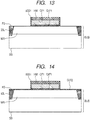
- the insulating spacer ISS1 is formed over the side wall of the first conductive film CF1, as illustrated in Fig. 13 .
- the material configuring the insulating spacer ISS1 is firstly formed to cover the first conductive film CF1.
- etch-back of the material configuring the formed insulating spacer ISS1 is secondly performed. This etch-back is performed until the upper surface of the first conductive film CF1 is exposed. As a result, the insulating spacer ISS 1 is formed over the side wall of the first conductive film CF1.
- the second gate insulating film GIF2 is formed over the first surface FS, as illustrated in Fig. 14 .
- the second gate insulating film GIF2 is formed by, for example, thermally oxidizing the first surface FS.
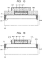
- the second conductive film CF2 is formed as illustrated in Fig. 15 .
- the second conductive film CF2 is formed to cover the first conductive film CF1 and the insulating spacer ISS1.
- the second conductive film CF2 is formed by, for example, CVD.
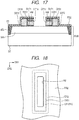
- the patterning of the first conductive film CF1 is performed (second patterning), as illustrated in Fig. 17 .
- a photoresist PR2 is firstly formed over the first conductive film CF1.
- the photoresist PR2 is secondly patterned by photolithography.
- the first conductive film CF1 is thirdly etched by using the photoresist PR2 having an opening in the second region R2 as a mask. This etching is performed by, for example, anisotropic etching such as RIE. As a result, the first conductive film CF1 remains to have the first coupling portion CF1a, the first memory gate portion CF1b, the second memory gate portion CF1c, and the second coupling portion CF1d.
- the distance between the first conductive film CF1 and the second conductive film CF2 is small at the cut positions. As a result, there is the fear in the semiconductor device according to the comparative example that the withstand voltage between the first conductive film CF1 and the second conductive film CF2 may be insufficient.
- the withstand voltage between the upper surface of the first conductive film CF1 and that of the second conductive film CF2 can be increased by the hard mask HM.
- An AHAO film has a higher dielectric constant than, for example, an ONO film. Therefore, the voltage to be applied to the first conductive film CF1 can be lowered. When the voltage to be applied to the first conductive film CF1 is lowered, the withstand voltage between the first conductive film CF1 and the second conductive film CF2 is easy to secure even if the thickness of the insulating spacer ISS1 is reduced.
- the cell area of the flash memory cell can be reduced. Also, in this case, the space between the first memory gate portion CF1b and the first control gate portion CF2b (the space between the second memory gate portion CF1c and the second control gate portion CF2c) can be reduced by reducing the thickness of the insulating spacer ISS1, and hence the current drive capability of the flash memory cell can be improved.
- the first memory gate portion CF1b and the second memory gate portion CF1c are coupled to each other, and hence the potential of the first memory gate portion CF1b and that of the second memory gate portion CF1c are equal to each other.
- the first control gate portion CF2b and the second control gate portion CF2c are coupled to each other, and hence the potential of the first control gate portion CF2b and that of the second control gate portion CF2c are equal to each other.
- the flash memory cell MC1 and the flash memory cell MC2 can be operated independently of each other.
- the semiconductor device according to First Embodiment has the wiring WL2c instead of the wiring WL2a and the wiring WL2b, the flash memory cell MC1 and the flash memory cell MC2 cannot be operated independently of each other.
- the semiconductor device according to First Embodiment can also be formed, for example, by forming the first conductive film CF1 to have the first coupling portion CF1a, the first memory gate portion CF1b, the second memory gate portion CF1c, and the second coupling portion CF1d with single patterning and by etching back the second conductive film CF2 formed to cover the first conductive film CF1.
- the second conductive film CF2 when the second conductive film CF2 is etched back, the second conductive film CF2 remains not only on the outer peripheral side of the first conductive film CF1 but also on the inner peripheral side thereof.
- the second conductive film CF2 remaining on the inner peripheral side of the first conductive film CF1 needs to be removed by etching.
- the second gate insulating film GIF2 under the second conductive film CF2 is removed by this etching. Because the second gate insulating film GIF2 is usually very thin, the semiconductor substrate SUB under the second gate insulating film GIF2 (specifically, the portion of the semiconductor substrate SUB where the source region SR is to be formed) is also partially removed.
- the first conductive film CF1 is formed to have the first coupling portion CF1a, the first memory gate portion CF1b, the second memory gate portion CF1c, and the second coupling portion CF1d by being subjected to double patterning (the first patterning step S4 and the second patterning step S9).
- the second patterning of the first conductive film CF1 (the second patterning step S9) is not performed at the time when the etch-back of the second conductive film CF2 (the etch-back step S8) is performed.
- the second conductive film CF2 remains only on the outer peripheral side of the first conductive film CF1 after the etch-back of the second conductive film CF2 is performed. Therefore, according to the manufacturing method of the semiconductor device of First Embodiment, the semiconductor substrate SUB in the portion where the source region SR is to be formed can be suppressed from being partially removed.
- the configuration of a semiconductor device according to Second Embodiment is the same as that of the semiconductor device according to First Embodiment in that the former includes the semiconductor substrate SUB, the first conductive film CF1, the second conductive film CF2, the first gate insulating film GIF1, the second gate insulating film GIF2, the insulating spacer ISS1, the wiring WL2a, and the wiring WL2b (or the wiring WL2c).
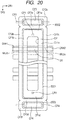
- the semiconductor device according to Second Embodiment further includes a third conductive film CF3, a fourth conductive film CF4, an insulating spacer ISS2, and an insulating spacer ISS3, as illustrated in Fig. 20 .
- the configuration of the semiconductor device according to Second Embodiment is different from that of the semiconductor device according to First Embodiment. In the following description, these differences will be mainly described.
- the third conductive film CF3 and the fourth conductive film CF4 extend along the first direction DR1.
- the third conductive film CF3 is arranged to be spaced apart from the first conductive film CF1 (the first coupling portion CF1a) in the second direction DR2.
- the fourth conductive film CF4 is arranged to be spaced apart from the first conductive film CF1 (the second coupling portion CF1d) in the second direction DR2. That is, the third conductive film CF3 sandwiches the third coupling portion CF2a with the first coupling portion CF1a in the second direction DR2, and the fourth conductive film CF4 sandwiches the fourth coupling portion CF2d with the second coupling portion CF1d in the second direction DR2.
- the third conductive film CF3 and the fourth conductive film CF4 have a third rectangular shape in plan view.
- the third rectangular shape has a side parallel to the first direction DR1 and a side parallel to the second direction DR2.
- the insulating spacer ISS2 surrounds the outer periphery of the third conductive film CF3 in plan view.
- the insulating spacer ISS3 surrounds the outer periphery of the fourth conductive film CF4 in plan view.
- the second conductive film CF2 surrounds the outer periphery of the third conductive film CF3 via the insulating spacer ISS2 and surrounds the outer periphery of the fourth conductive film CF4 via the insulating spacer ISS3. More specifically, the second conductive film CF2 further includes a fifth coupling portion CF2e and a sixth coupling portion CF2f.
- the fifth coupling portion CF2e surrounds, with the third coupling portion CF2a, the outer periphery of the third conductive film CF3 in plan view.
- the sixth coupling portion CF2f surrounds, with the fourth coupling portion CF2d, the outer periphery of the fourth conductive film CF4 in plan view.
- the contact plug CP3 is electrically coupled to the fifth coupling portion CF2e.
- the contact plug CP4 is electrically coupled to the sixth coupling portion CF2f. From another point of view, this means that the fifth coupling portion CF2e and the sixth coupling portion CF2f serve as a shunt region of the second conductive film CF2.
- the contact plug CP3 (contact plug CP4) is arranged to straddle the fifth coupling portion CF2e and to reach the third conductive film CF3 (to straddle the sixth coupling portion CF2f and to reach the fourth conductive film CF4).
- the third conductive film CF3 and the fourth conductive film CF4 are electrically separated from the first conductive film CF1 by the insulating spacer ISS2 and the insulating spacer ISS3, respectively. Therefore, even if the contact plug CP3 is arranged to reach the third conductive film CF3 (the contact plug CP4 is arranged to reach the fourth conductive film CF4), the first conductive film CF1 and the second conductive film CF2 are not short-circuited.
- a manufacturing method of the semiconductor device includes the semiconductor substrate provision step S1, the first gate insulating film formation step S2, the first conductive film formation step S3, the first patterning step S4, the insulating spacer formation step S5, the second gate insulating film formation step S6, the second conductive film formation step S7, the etch-back step S8, and the second patterning step S9.
- the first patterning step S4 includes the hard mask formation step S41, the hard mask patterning step S42, and the etching step S43. Regarding these points, the manufacturing method of the semiconductor device according to Second Embodiment is the same as that of the semiconductor device according to First Embodiment.
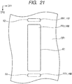
- the hard mask HM (and photoresist PR1) is patterned to cover the first region R1, the third region R3, and the fourth region R4, as illustrated in Fig. 21 .
- the third region R3 is spaced apart from the first region R1 in the second direction DR2.
- the fourth region R4 is spaced apart from the first region R1 in the second direction DR2.
- the third region R3 and the fourth region R4 have the third rectangular shape in plan view.
- the third region R3 and the fourth region R4 are located opposite to each other with respect to the first region R1 in the second direction DR2. Therefore, the first conductive film CF1 is patterned in the etching step S43 such that the third conductive film CF3 and the fourth conductive film CF4 remain in addition to the first conductive film CF1.
- the insulating spacer ISS1 is formed over the side wall of the first conductive film CF1
- the insulating spacer ISS2 is formed over the side wall of the third conductive film CF3
- the insulating spacer ISS3 is formed over the side wall of the fourth conductive film CF4 in the insulating spacer formation step S5.
- the third conductive film CF3 and the fourth conductive film CF4 are formed at the time when the etch-back step S8 is performed, as illustrated in Fig. 22 . Therefore, the second conductive film CF2 remains along the side walls of the third conductive film CF3 and the fourth conductive film CF4 by performing etch-back in the etch-back step S8. The remaining second conductive film CF2 serves as the fifth coupling portion CF2e and the sixth coupling portion CF2f.
- the width of the shunt region of the second conductive film CF2 cannot be made equal to or larger than the width of the third coupling portion CF2a (the width of the fourth coupling portion CF2d). Therefore, when any mask shift occurs in forming the contact hole CH, there is the fear that: the contact plug CP3 may not be electrically coupled to the third coupling portion CF2a (the contact plug CP4 may not be electrically coupled to the fourth coupling portion CF2d); or the contact plug CP3 may be electrically coupled to both the first coupling portion CF1a and the third coupling portion CF2a (the contact plug CP4 may be electrically coupled to both the second coupling portion CF1d and the fourth coupling portion CF2d).
- the contact plug CP 3 may be formed to straddle the fifth coupling portion CF2e and the third conductive film CF3 (the contact plug CP4 may be formed to straddle the sixth coupling portion CF2f and the fourth conductive film CF4), and hence the shunt region of the second conductive film CF2 can be secured relatively widely. Therefore, according to the semiconductor device of Second Embodiment, the following situations can be suppressed in which: the contact plug CP3 (the contact plug CP4) may not be electrically coupled to the second conductive film CF2; and the first conductive film CF1 and the second conductive film CF2 may be short-circuited.
- the configuration of a semiconductor device according to Third Embodiment is the same as that of the semiconductor device according to First Embodiment in that the former includes the semiconductor substrate SUB, the first conductive film CF1, the second conductive film CF2, the first gate insulating film GIF1, the second gate insulating film GIF2, the insulating spacer ISS1, and the wiring WL2c.
- a first cut surface CS1 and a second cut surface CS2 are provided in the first memory gate portion CF1b, and a third cut surface CS3 and a fourth cut surface CS4 are provided in the second memory gate portion CF1c, as illustrated in Fig. 23 .
- a fifth cut surface CS5 and a sixth cut surface CS6 are provided in the first control gate portion CF2b, and a seventh cut surface CS7 and an eighth cut surface CS8 are provided in the second control gate portion CF2c.
- the first cut surface CS1 and the second cut surface CS2 cross the second direction DR2.
- the first cut surface CS1 and the second cut surface CS2 preferably cross the second direction DR2 at right angles.
- the first cut surface CS1 and the second cut surface CS2 face each other by being spaced apart from each other in the second direction DR2. That is, the first memory gate portion CF1b is removed between the first cut surface CS1 and the second cut surface CS2.
- the fifth cut surface CS5 and the sixth cut surface CS6 cross the second direction DR2.
- the fifth cut surface CS5 and the sixth cut surface CS6 preferably cross the second direction DR2 at right angles.
- the fifth cut surface CS5 and the sixth cut surface CS6 face each other by being spaced apart from each other in the second direction DR2. That is, the first control gate portion CF2b is removed between the fifth cut surface CS5 and the sixth cut surface CS6.
- the seventh cut surface CS7 and the eighth cut surface CS8 cross the second direction DR2.
- the seventh cut surface CS7 and the eighth cut surface CS8 preferably cross the second direction DR2 at right angles.
- the seventh cut surface CS 7 and the eighth cut surface CS8 face each other by being spaced apart from each other in the second direction DR2. That is, the second control gate portion CF2c is removed between the seventh cut surface CS7 and the eighth cut surface CS8.
- the first cut surface CS1 and the second cut surface CS2 are located between the fifth cut surface CS5 and the sixth cut surface CS6 in plan view.
- the third cut surface CS3 and the fourth cut surface CS4 are located between the seventh cut surface CS7 and the eighth cut surface CS8 in plan view. That is, the first control gate portion CF2b is removed in a wider range in the second direction DR2 than the first memory gate portion CF1b, and the second control gate portion CF2c is removed in a wider range in the second direction DR2 than the second memory gate portion CF1c.
- a manufacturing method of the semiconductor device includes the semiconductor substrate provision step S1, the first gate insulating film formation step S2, the first conductive film formation step S3, the first patterning step S4, the insulating spacer formation step S5, the second gate insulating film formation step S6, the second conductive film formation step S7, the etch-back step S8, and the second patterning step S9.
- the first patterning step S4 has the hard mask formation step S41, the hard mask patterning step S42, and the etching step S43. Regarding these points, the manufacturing method of the semiconductor device according to Third Embodiment is the same as that of the semiconductor device according to First Embodiment.
- the third patterning step S10 is performed after the etch-back step S8 and before the second patterning step S9.
- a photoresist PR3 is firstly formed.
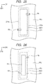
- the photoresist PR 3 has openings in a fifth region R5 and a sixth region R6, as illustrated in Fig. 25 .
- the fifth region R5 and the sixth region R6 have a fourth rectangular shape.
- the fourth rectangular shape has a side parallel to the first direction DR1 and a side parallel to the second direction DR2.
- the fifth region R5 is arranged to straddle the first control gate portion CF2b along the first direction DR1 and to reach the first conductive film CF1.
- the sixth region R6 is arranged to straddle the second control gate portion CF2c along the first direction DR1 and to reach the first conductive film CF1.
- the fifth cut surface CS5, the sixth cut surface CS6, the seventh cut surface CS7, and the eighth cut surface CS8 can be formed even if any mask shift along the first direction DR1 occurs when the photoresist PR3 is formed.
- the fifth region R5 and the sixth region R6 are arranged to reach the first conductive film CF1 in the first direction DR1, the first conductive film CF1 is not etched in the third patterning step S10, because the hard mask HM is located over the upper surface of the first conductive film CF1.
- etching is secondly performed by using the photoresist PR3.
- This etching is, for example, anisotropic etching such as RIE.
- the first control gate portion CF2b is partially removed, so that the fifth cut surface CS5 and the sixth cut surface CS6 are formed.
- the second control gate portion CF2c is partially removed by this etching, so that the seventh cut surface CS7 and the eighth cut surface CS8 are formed.
- openings are provided in the second region R2, the seventh region R7, and the eighth region R8 of the photoresist PR2, as illustrated in Fig. 26 .
- the seventh region R7 and the eighth region R8 have a fifth rectangular shape.
- the fifth rectangular shape has a side parallel to the first direction DR1 and a side parallel to the second direction DR2 in plan view.
- the widths of the seventh region R7 and the eighth region R8 in the second direction DR2 are smaller than those of the fifth region R5 and the sixth region R6 in the second direction DR2.
- the seventh region R7 is arranged such that it overlaps the fifth region R5 in the second direction DR2 and the end, in the first direction DR1, of it reaches the second region R2.
- the eighth region R8 is arranged such that it overlaps the sixth region R6 in the second direction DR2 and the end, in the first direction DR1, of it reaches the second region R2.
- the first coupling portion CF1a, the first memory gate portion CF1b provided with the first cut surface CS1 and the second cut surface CS2, the second memory gate portion CF1c provided with the third cut face CS3 and the fourth cut face CS4, and the second coupling portion CF1d are formed.
- the first memory gate portion CF1b, the second memory gate portion CF1c, the first control gate portion CF2b, and the second control gate portion CF2c are cut in the middle. Therefore, the flash memory cell MC1 and the flash memory cell MC2 can be operated independently of each other in the semiconductor device according to Third Embodiment.
- the cut surface provided in the first control gate portion CF2b recedes from the cut surface provided in the first memory gate portion CF1b
- the cut surface provided in the second control gate portion CF2c recedes from the cut surface provided in the second memory gate portion CF1c. Therefore, according to the semiconductor device of Third Embodiment, the withstand voltage between the first conductive film CF1 and the second conductive film CF2 is easy to secure, even if the first conductive film CF1 and the second conductive film CF2 have a cut surface.
Landscapes
- Semiconductor Memories (AREA)
- Non-Volatile Memory (AREA)
Applications Claiming Priority (1)
| Application Number | Priority Date | Filing Date | Title |
|---|---|---|---|
| JP2018040612A JP7026537B2 (ja) | 2018-03-07 | 2018-03-07 | 半導体装置及び半導体装置の製造方法 |
Publications (2)
| Publication Number | Publication Date |
|---|---|
| EP3537477A2 true EP3537477A2 (de) | 2019-09-11 |
| EP3537477A3 EP3537477A3 (de) | 2020-07-22 |
Family
ID=65363061
Family Applications (1)
| Application Number | Title | Priority Date | Filing Date |
|---|---|---|---|
| EP19155607.5A Withdrawn EP3537477A3 (de) | 2018-03-07 | 2019-02-05 | Halbleiterbauelement und verfahren zur herstellung eines halbleiterbauelements |
Country Status (4)
| Country | Link |
|---|---|
| US (1) | US10847628B2 (de) |
| EP (1) | EP3537477A3 (de) |
| JP (1) | JP7026537B2 (de) |
| CN (1) | CN110246845B (de) |
Families Citing this family (1)
| Publication number | Priority date | Publication date | Assignee | Title |
|---|---|---|---|---|
| JP2021082656A (ja) * | 2019-11-15 | 2021-05-27 | ルネサスエレクトロニクス株式会社 | 半導体装置 |
Citations (1)
| Publication number | Priority date | Publication date | Assignee | Title |
|---|---|---|---|---|
| JP2015103698A (ja) | 2013-11-26 | 2015-06-04 | ルネサスエレクトロニクス株式会社 | 半導体装置および半導体装置の製造方法 |
Family Cites Families (13)
| Publication number | Priority date | Publication date | Assignee | Title |
|---|---|---|---|---|
| US7655536B2 (en) | 2005-12-21 | 2010-02-02 | Sandisk Corporation | Methods of forming flash devices with shared word lines |
| JP4171032B2 (ja) | 2006-06-16 | 2008-10-22 | 株式会社東芝 | 半導体装置及びその製造方法 |
| JP5521555B2 (ja) * | 2008-02-20 | 2014-06-18 | 日本電気株式会社 | 不揮発性記憶装置およびその製造方法 |
| JP5404149B2 (ja) * | 2009-04-16 | 2014-01-29 | ルネサスエレクトロニクス株式会社 | 半導体記憶装置 |
| US8803214B2 (en) * | 2010-06-28 | 2014-08-12 | Micron Technology, Inc. | Three dimensional memory and methods of forming the same |
| TWI479653B (zh) * | 2012-12-18 | 2015-04-01 | Macronix Int Co Ltd | 半導體結構及其製造方法 |
| KR20150028189A (ko) | 2013-09-05 | 2015-03-13 | 르네사스 일렉트로닉스 가부시키가이샤 | 반도체 장치 및 그 제조 방법 |
| US9412597B2 (en) * | 2013-12-05 | 2016-08-09 | Taiwan Semiconductor Manufacturing Co., Ltd. | Flash memory semiconductor device and method thereof |
| US9391085B2 (en) | 2014-08-08 | 2016-07-12 | Taiwan Semiconductor Manufacturing Co., Ltd. | Self-aligned split gate flash memory having liner-separated spacers above the memory gate |
| WO2016060014A1 (ja) | 2014-10-15 | 2016-04-21 | 株式会社フローディア | 半導体装置およびその製造方法 |
| JP6385873B2 (ja) | 2015-03-30 | 2018-09-05 | ルネサスエレクトロニクス株式会社 | 半導体装置およびその製造方法 |
| JP5905630B1 (ja) * | 2015-08-13 | 2016-04-20 | 株式会社フローディア | 半導体集積回路装置の製造方法、および半導体集積回路装置 |
| JP5951096B1 (ja) | 2015-10-01 | 2016-07-13 | 株式会社フローディア | 不揮発性半導体記憶装置 |
-
2018
- 2018-03-07 JP JP2018040612A patent/JP7026537B2/ja active Active
-
2019
- 2019-02-05 EP EP19155607.5A patent/EP3537477A3/de not_active Withdrawn
- 2019-02-22 US US16/282,864 patent/US10847628B2/en active Active
- 2019-03-05 CN CN201910165538.0A patent/CN110246845B/zh active Active
Patent Citations (1)
| Publication number | Priority date | Publication date | Assignee | Title |
|---|---|---|---|---|
| JP2015103698A (ja) | 2013-11-26 | 2015-06-04 | ルネサスエレクトロニクス株式会社 | 半導体装置および半導体装置の製造方法 |
Also Published As
| Publication number | Publication date |
|---|---|
| CN110246845A (zh) | 2019-09-17 |
| EP3537477A3 (de) | 2020-07-22 |
| JP7026537B2 (ja) | 2022-02-28 |
| JP2019160828A (ja) | 2019-09-19 |
| US10847628B2 (en) | 2020-11-24 |
| US20190280096A1 (en) | 2019-09-12 |
| CN110246845B (zh) | 2024-06-21 |
Similar Documents
| Publication | Publication Date | Title |
|---|---|---|
| KR102691496B1 (ko) | 반도체 장치 | |
| JP3311070B2 (ja) | 半導体装置 | |
| KR102344881B1 (ko) | 반도체 장치 및 반도체 장치의 제조 방법 | |
| TW202220146A (zh) | 記憶體裝置 | |
| US8421146B2 (en) | Semiconductor device having vertical transistor, manufacturing method thereof, and data processing system | |
| TW202201649A (zh) | 記憶體裝置 | |
| KR102588209B1 (ko) | 반도체 소자 및 이의 제조 방법 | |
| US8994080B2 (en) | Stacked carbon-based FETs | |
| JPH11354749A (ja) | 半導体集積回路装置およびその製造方法 | |
| US20210375931A1 (en) | Ferroelectric memory device and method of forming the same | |
| KR102675909B1 (ko) | 반도체 소자 | |
| US20220367515A1 (en) | Ferroelectric memory device and method of forming the same | |
| CN103050380A (zh) | 半导体器件的形成方法 | |
| TW202145542A (zh) | 鐵電記憶體裝置及其形成方法 | |
| KR101804420B1 (ko) | 반도체 소자 및 그 제조 방법 | |
| EP3537477A2 (de) | Halbleiterbauelement und verfahren zur herstellung eines halbleiterbauelements | |
| KR20240009650A (ko) | 반도체 소자 | |
| WO2026031683A1 (zh) | 垂直电荷转移成像传感器及其制造方法 | |
| TWI901757B (zh) | 半導體元件 | |
| CN111326516A (zh) | 非挥发性存储器结构及其制造方法 | |
| KR20240156857A (ko) | 반도체 장치 | |
| KR100431709B1 (ko) | 수직방향의채널을갖는모스트랜지스터와그를포함하는반도체메모리셀및그제조방법 | |
| CN119486115B (zh) | 一种半导体器件及其制造方法、电子设备 | |
| JP2005203455A (ja) | 半導体装置およびその製造方法 | |
| KR20040099110A (ko) | 반도체 장치 |
Legal Events
| Date | Code | Title | Description |
|---|---|---|---|
| PUAI | Public reference made under article 153(3) epc to a published international application that has entered the european phase |
Free format text: ORIGINAL CODE: 0009012 |
|
| STAA | Information on the status of an ep patent application or granted ep patent |
Free format text: STATUS: THE APPLICATION HAS BEEN PUBLISHED |
|
| AK | Designated contracting states |
Kind code of ref document: A2 Designated state(s): AL AT BE BG CH CY CZ DE DK EE ES FI FR GB GR HR HU IE IS IT LI LT LU LV MC MK MT NL NO PL PT RO RS SE SI SK SM TR |
|
| AX | Request for extension of the european patent |
Extension state: BA ME |
|
| RIC1 | Information provided on ipc code assigned before grant |
Ipc: H01L 27/11565 20170101ALI20191219BHEP Ipc: H01L 21/28 20060101ALI20191219BHEP Ipc: H01L 29/423 20060101ALI20191219BHEP Ipc: H01L 27/11568 20170101AFI20191219BHEP |
|
| PUAL | Search report despatched |
Free format text: ORIGINAL CODE: 0009013 |
|
| AK | Designated contracting states |
Kind code of ref document: A3 Designated state(s): AL AT BE BG CH CY CZ DE DK EE ES FI FR GB GR HR HU IE IS IT LI LT LU LV MC MK MT NL NO PL PT RO RS SE SI SK SM TR |
|
| AX | Request for extension of the european patent |
Extension state: BA ME |
|
| RIC1 | Information provided on ipc code assigned before grant |
Ipc: H01L 21/28 20060101ALI20200617BHEP Ipc: H01L 27/11565 20170101ALI20200617BHEP Ipc: H01L 29/423 20060101ALI20200617BHEP Ipc: H01L 27/11568 20170101AFI20200617BHEP |
|
| STAA | Information on the status of an ep patent application or granted ep patent |
Free format text: STATUS: THE APPLICATION IS DEEMED TO BE WITHDRAWN |
|
| 18D | Application deemed to be withdrawn |
Effective date: 20210123 |