EP3528271A1 - Harzstruktur, elektronische vorrichtung und herstellungsverfahren für harzstruktur - Google Patents
Harzstruktur, elektronische vorrichtung und herstellungsverfahren für harzstruktur Download PDFInfo
- Publication number
- EP3528271A1 EP3528271A1 EP17861033.3A EP17861033A EP3528271A1 EP 3528271 A1 EP3528271 A1 EP 3528271A1 EP 17861033 A EP17861033 A EP 17861033A EP 3528271 A1 EP3528271 A1 EP 3528271A1
- Authority
- EP
- European Patent Office
- Prior art keywords
- button unit
- push
- receptacle
- terminal
- type switch
- Prior art date
- Legal status (The legal status is an assumption and is not a legal conclusion. Google has not performed a legal analysis and makes no representation as to the accuracy of the status listed.)
- Granted
Links
Images


Classifications
-
- H—ELECTRICITY
- H01—ELECTRIC ELEMENTS
- H01H—ELECTRIC SWITCHES; RELAYS; SELECTORS; EMERGENCY PROTECTIVE DEVICES
- H01H13/00—Switches having rectilinearly-movable operating part or parts adapted for pushing or pulling in one direction only, e.g. push-button switch
- H01H13/70—Switches having rectilinearly-movable operating part or parts adapted for pushing or pulling in one direction only, e.g. push-button switch having a plurality of operating members associated with different sets of contacts, e.g. keyboard
- H01H13/86—Switches having rectilinearly-movable operating part or parts adapted for pushing or pulling in one direction only, e.g. push-button switch having a plurality of operating members associated with different sets of contacts, e.g. keyboard characterised by the casing, e.g. sealed casings or casings reducible in size
-
- H—ELECTRICITY
- H01—ELECTRIC ELEMENTS
- H01H—ELECTRIC SWITCHES; RELAYS; SELECTORS; EMERGENCY PROTECTIVE DEVICES
- H01H9/00—Details of switching devices, not covered by groups H01H1/00 - H01H7/00
- H01H9/02—Bases, casings, or covers
- H01H9/0271—Bases, casings, or covers structurally combining a switch and an electronic component
-
- H—ELECTRICITY
- H01—ELECTRIC ELEMENTS
- H01H—ELECTRIC SWITCHES; RELAYS; SELECTORS; EMERGENCY PROTECTIVE DEVICES
- H01H1/00—Contacts
- H01H1/12—Contacts characterised by the manner in which co-operating contacts engage
- H01H1/14—Contacts characterised by the manner in which co-operating contacts engage by abutting
- H01H1/20—Bridging contacts
-
- H—ELECTRICITY
- H01—ELECTRIC ELEMENTS
- H01H—ELECTRIC SWITCHES; RELAYS; SELECTORS; EMERGENCY PROTECTIVE DEVICES
- H01H1/00—Contacts
- H01H1/58—Electric connections to or between contacts; Terminals
- H01H1/5805—Connections to printed circuits
-
- H—ELECTRICITY
- H01—ELECTRIC ELEMENTS
- H01H—ELECTRIC SWITCHES; RELAYS; SELECTORS; EMERGENCY PROTECTIVE DEVICES
- H01H11/00—Apparatus or processes specially adapted for the manufacture of electric switches
-
- H—ELECTRICITY
- H01—ELECTRIC ELEMENTS
- H01H—ELECTRIC SWITCHES; RELAYS; SELECTORS; EMERGENCY PROTECTIVE DEVICES
- H01H13/00—Switches having rectilinearly-movable operating part or parts adapted for pushing or pulling in one direction only, e.g. push-button switch
- H01H13/70—Switches having rectilinearly-movable operating part or parts adapted for pushing or pulling in one direction only, e.g. push-button switch having a plurality of operating members associated with different sets of contacts, e.g. keyboard
- H01H13/88—Processes specially adapted for manufacture of rectilinearly movable switches having a plurality of operating members associated with different sets of contacts, e.g. keyboards
-
- H—ELECTRICITY
- H01—ELECTRIC ELEMENTS
- H01H—ELECTRIC SWITCHES; RELAYS; SELECTORS; EMERGENCY PROTECTIVE DEVICES
- H01H21/00—Switches operated by an operating part in the form of a pivotable member acted upon directly by a solid body, e.g. by a hand
-
- H—ELECTRICITY
- H05—ELECTRIC TECHNIQUES NOT OTHERWISE PROVIDED FOR
- H05K—PRINTED CIRCUITS; CASINGS OR CONSTRUCTIONAL DETAILS OF ELECTRIC APPARATUS; MANUFACTURE OF ASSEMBLAGES OF ELECTRICAL COMPONENTS
- H05K1/00—Printed circuits
- H05K1/18—Printed circuits structurally associated with non-printed electric components
- H05K1/182—Printed circuits structurally associated with non-printed electric components associated with components mounted in printed circuit boards [PCB], e.g. insert-mounted components [IMC]
- H05K1/185—Printed circuits structurally associated with non-printed electric components associated with components mounted in printed circuit boards [PCB], e.g. insert-mounted components [IMC] associated with components encapsulated in the insulating substrate of the PCBs; associated with components incorporated in internal layers of multilayer circuit boards
-
- H—ELECTRICITY
- H01—ELECTRIC ELEMENTS
- H01H—ELECTRIC SWITCHES; RELAYS; SELECTORS; EMERGENCY PROTECTIVE DEVICES
- H01H13/00—Switches having rectilinearly-movable operating part or parts adapted for pushing or pulling in one direction only, e.g. push-button switch
- H01H13/02—Details
- H01H13/04—Cases; Covers
-
- H—ELECTRICITY
- H01—ELECTRIC ELEMENTS
- H01H—ELECTRIC SWITCHES; RELAYS; SELECTORS; EMERGENCY PROTECTIVE DEVICES
- H01H13/00—Switches having rectilinearly-movable operating part or parts adapted for pushing or pulling in one direction only, e.g. push-button switch
- H01H13/70—Switches having rectilinearly-movable operating part or parts adapted for pushing or pulling in one direction only, e.g. push-button switch having a plurality of operating members associated with different sets of contacts, e.g. keyboard
- H01H13/702—Switches having rectilinearly-movable operating part or parts adapted for pushing or pulling in one direction only, e.g. push-button switch having a plurality of operating members associated with different sets of contacts, e.g. keyboard with contacts carried by or formed from layers in a multilayer structure, e.g. membrane switches
-
- H—ELECTRICITY
- H01—ELECTRIC ELEMENTS
- H01H—ELECTRIC SWITCHES; RELAYS; SELECTORS; EMERGENCY PROTECTIVE DEVICES
- H01H9/00—Details of switching devices, not covered by groups H01H1/00 - H01H7/00
- H01H9/02—Bases, casings, or covers
- H01H2009/0285—Casings overmoulded over assembled switch or relay
-
- H—ELECTRICITY
- H01—ELECTRIC ELEMENTS
- H01H—ELECTRIC SWITCHES; RELAYS; SELECTORS; EMERGENCY PROTECTIVE DEVICES
- H01H2229/00—Manufacturing
- H01H2229/044—Injection moulding
-
- H—ELECTRICITY
- H01—ELECTRIC ELEMENTS
- H01H—ELECTRIC SWITCHES; RELAYS; SELECTORS; EMERGENCY PROTECTIVE DEVICES
- H01H2239/00—Miscellaneous
- H01H2239/058—Containing a battery
-
- H—ELECTRICITY
- H01—ELECTRIC ELEMENTS
- H01H—ELECTRIC SWITCHES; RELAYS; SELECTORS; EMERGENCY PROTECTIVE DEVICES
- H01H3/00—Mechanisms for operating contacts
- H01H3/02—Operating parts, i.e. for operating driving mechanism by a mechanical force external to the switch
- H01H3/04—Levers
-
- H—ELECTRICITY
- H01—ELECTRIC ELEMENTS
- H01H—ELECTRIC SWITCHES; RELAYS; SELECTORS; EMERGENCY PROTECTIVE DEVICES
- H01H3/00—Mechanisms for operating contacts
- H01H3/02—Operating parts, i.e. for operating driving mechanism by a mechanical force external to the switch
- H01H3/12—Push-buttons
-
- H—ELECTRICITY
- H01—ELECTRIC ELEMENTS
- H01H—ELECTRIC SWITCHES; RELAYS; SELECTORS; EMERGENCY PROTECTIVE DEVICES
- H01H9/00—Details of switching devices, not covered by groups H01H1/00 - H01H7/00
- H01H9/02—Bases, casings, or covers
-
- H—ELECTRICITY
- H05—ELECTRIC TECHNIQUES NOT OTHERWISE PROVIDED FOR
- H05K—PRINTED CIRCUITS; CASINGS OR CONSTRUCTIONAL DETAILS OF ELECTRIC APPARATUS; MANUFACTURE OF ASSEMBLAGES OF ELECTRICAL COMPONENTS
- H05K2201/00—Indexing scheme relating to printed circuits covered by H05K1/00
- H05K2201/10—Details of components or other objects attached to or integrated in a printed circuit board
- H05K2201/10007—Types of components
- H05K2201/10037—Printed or non-printed battery
-
- H—ELECTRICITY
- H05—ELECTRIC TECHNIQUES NOT OTHERWISE PROVIDED FOR
- H05K—PRINTED CIRCUITS; CASINGS OR CONSTRUCTIONAL DETAILS OF ELECTRIC APPARATUS; MANUFACTURE OF ASSEMBLAGES OF ELECTRICAL COMPONENTS
- H05K2201/00—Indexing scheme relating to printed circuits covered by H05K1/00
- H05K2201/10—Details of components or other objects attached to or integrated in a printed circuit board
- H05K2201/10007—Types of components
- H05K2201/10053—Switch
Definitions
- the present invention relates generally to a resin structure, an electronic device, and a method of manufacturing a resin structure. More specifically, the present invention relates to a package structure for the push-type switch that provides a click sensation when operated, and a method of manufacturing the package structure.
- the package structure is suitable for manufacturing an electronic device wherein the push-type switch is assembled with another electronic device.
- a push-type switch may be used as a component that is made up of an electrical circuit.
- the push-type switch must provide a user with a sense of operating the device (a click sensation).
- the advantage is that provide a user with a sense of operating the device allows the user to reliably recognize having pressed a switch. For instance, a tactile switch is one such type of switch.
- the push-type switch is typically placed on a printed substrate that holds an electrical circuit; the push-type switch is for accepting an operation from a person and entering a signal into the electrical circuit.
- FIG. 13 is a top view for describing the typical package structure of a push-type switch; and
- FIG. 14 is a cross-sectional view of the cross-section XIV-XIV in the package structure depicted in FIG. 13 .
- the push-type switch 100 may be connected to another electronic component by soldering a connection 210 onto the printed circuit board 200 on which the relevant electronic component is mounted (not shown).
- the connection 210 connects terminals 110, 111 and the conductive circuitry 201 on the printed circuit board.
- the electronic device that uses the push-type switch 100 is further processed by assembling the printed circuit board 200 and a resin structure 320 provided with a hole 321 that can accommodate the push-type switch 100 internally; and a sheet 310 is bonded over the upper surface of the resin structure 320 to cover the hole 321.
- an electronic device thus configured is larger because the storage space (i.e., the hole 321) into which the push-type switch 100 is mounted must be wider; the manufacturing cost increases because the manufacturing process is more complicated since the sheet material 310 must be bonded to cover the storage space; or the electronic device loses its design flexibility.
- the ability to provide these features has limitations since the printed substrate is used when assembling the push-type button switch with other electronic components
- Japanese Patent Publication 2003-165357 ( FIG. 3B ) proposes embedding the mechanical operational structure of the push-type switch into a resin structure as a means of either omitting the switch storage space, or the sheet material on the outer surface.
- JP 2003-165357 A provides no discussion in terms of the proposed method, on a means of assembling the push-type switch with another related component. If an existing printed substrate is used for configuring the electronic device, the assembly structure instead becomes more complicated.
- the drive unit (button unit) for the push-type switch is embedded in an elastic resin such as a polyester elastomer in the device proposed by Japanese Patent Publication JP H6-349377A ( FIG. 3A ); JP H6-349377A further proposes a switch structure where the conductive part provided at tip end of the button unit allows electrical conduction to the conduction circuit provided on the printed substrate.
- the switch structure proposed in said existing technology is problematic in that no click sensation is produced when the button unit is pressed, i.e., during the switching. Another issue is the increased manufacturing cost which is due to the need to align the conduction circuit provided on the printed substrate and the button unit circuitry.
- the printed substrate also remains an impediment to resolving the problem of providing a thinner profile.
- the present invention provides for a compact, thin, electronic device that uses a push-type switch that provides a click sensation when pressed, which can be manufactured at low cost.
- the present invention is a resin structure including a molded resin element and a push-type switch.
- the push-type switch includes a first terminal and a second terminal configured to connect to an electrical circuit; a receptacle whereon the first terminal and the second terminal are secured; a button unit protruding from the receptacle; and a contact spring unit configured to move with the button unit, to electrically connect between the first terminal and the second terminal, and to generate an opposing force relative to a pressure applied between the receptacle and the button unit; the receptacle configured to store the button unit and the contact spring unit; and the receptacle of the push-type switch embedded in the molded resin element with the button unit exposed from the molded resin element.
- the molded resin element may be composed of an elastic material.
- the resin structure includes a first outer surface where from the button unit is exposed, and a second outer surface facing the first outer surface; and the resin structure elastically deforms when the receptacle receives pressure from the second outer surface causing the receptacle to move from the second outer surface toward the first outer surface.
- the receptacle may be embedded in the molded resin element so that the button unit is receded from the first outer surface which surrounds the button unit in the molded resin element.
- the molded resin element may include a beam structure and a support supporting the beam structure.
- the push-type switch may be embedded in the beam structure of the molded resin element.
- the resin structure may further include: an electronic component embedded in the molded resin element and configured for electrically connecting to the push-type switch; and a conductive wiring pattern formed on the outer surface of the molded resin element and configured to connect the electrical component and the first terminal.
- an electronic device is provided with the above-mentioned resin structure, and a contacting part placed at the first outer surface of the molded resin element; and the molded resin element is configured to deform so that the button unit touches the contacting part when the receptacle receives pressure from the second outer surface.
- the contacting part may be a battery.
- the push-type switch includes a first terminal and a second terminal configured to connect to an electrical circuit; a receptacle whereon the first terminal and the second terminal are secured; a button unit protruding from the receptacle; and a contact spring unit configured to move with the button unit, to electrically connect between the first terminal and the second terminal, and to generate an opposing force relative to a pressure applied between the receptacle and the button unit; the receptacle configured to store the button unit and the contact spring unit; and the method of manufacturing the resin structure includes: placing the push-type switch in a mold with the mold pressing the button unit of the push-type switch toward the receptacle so that the button unit is separate from a cavity when the cavity is filled with resin; and injecting a resin into the cavity in the mold.
- the present invention provides for a resin structure with a built-in switch where the resin structure establishes an operational feel for the switch and contributes to a compact and thin electronic device.
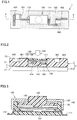
- FIG. 1 is a plan view illustrating a configuration of a resin structure according to a first embodiment
- FIG. 2 is a cross-sectional view along a cross section II-II in FIG. 1 .
- the resin structure 1 is provided with a molded resin element 420, a push-type switch 100, and electronic components 430, 440.
- the push-type switch 100 is embedded in the molded resin elements 420 along with the electronic components 430, 440.
- the molded resin element 420 is an elastic material in the first embodiment, e.g., an elastomer that can be an injection molded component.
- FIG. 3 is a cross-sectional view illustrating a configuration of a push type switch 100 embedded in the resin structure 1.
- the push-type switch 100 includes a first terminal 110 and a second terminal 111, a receptacle 140, a button unit 160, and a contact spring Unit 150.
- the receptacle 140 includes a base 130 and a cover 120.
- the first terminal 110 and the second terminal 111 are secured to the base 130 of the receptacle 140.
- the button unit 160 protrudes from the cover 120 of the receptacle 140 when not subject to pressure.
- the receptacle 140 houses the button unit 160 and the contact spring unit 150.
- the inner end parts of the first terminal 110 and the second terminal 111 are exposed as fixed contacts on the base 130 at the bottom of the storage space; the contact spring unit 150 operates as a movable contact.
- the cover 120 covers the base 130 from opposite the first terminal 110 and the second terminal 111 so that the button unit 160 and the contact spring unit 150 do not escape from the base 130.
- the contact spring unit 150 may be a metallic leaf spring, and configured to move with the button unit 160.
- the contact spring unit 150 may be curved with the convex portion toward slightly toward the button unit 160 to provide a click sensation when the button is pressed.
- the contact spring unit 150 electrically connects between the first terminal 110 and the second terminal 111 when the button unit is pressed and the bottom surface of the base 130 warps into a convex surface; additionally, the contact spring unit 150 is configured to generate an opposing force relative to the pressure 400 added between the base 130 and the button unit 160.
- the first terminal 110 and the second terminal 111 are connected to the electrical circuits at the outer surface of the molded resin element.
- the base 130 of the push-type switch 100 is embedded in the molded resin element 420 with the button unit 160 exposed from the molded resin element 420.
- the resin structure 1 further includes: an electronic component 430 that is embedded in the molded resin element 420 and can be electrically connected to the push-type switch 100; and a conductive wiring pattern 401 formed on the outer surface of the molded resin element 420 and connecting the electronic component and the first terminal 110.
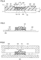
- FIG. 4 is a cross-sectional view illustrating the deformation in the enclosure surrounding the push-type switch 100 when pressure is added to the resin structure 1.
- the resin structure 1 includes a first outer surface F1 and a second outer surface F2 that faces the first outer surface F1; the button unit 160 is exposed from the first outer surface F1.
- the base 130 is placed closer to the second outer surface F2 than the button unit 160 in the resin structure 1.
- the molded resin element 420 elastically deforms when the base 130 receives pressure 400 from the second outer surface F2, which causes the base 130 to move from the second outer surface F2 toward the first outer surface F1.
- An electronic device 2 is provided with the resin structure 1, and a contacting part 410 placed at the first outer surface F1 of the molded resin element.
- the contacting part 410 may be a battery, or another component such as an enclosure.
- the contacting part 410 is preferably of a material that has a lower elasticity than the molded resin element 420.
- the molded resin element 420 deforms so that the button unit 160 touches the contacting part 410 when the base 130 receives a pressure 400 from second outer surface F2 as illustrated in FIG. 4 .
- the molded resin element 420 returns to the shape illustrated in FIG. 2 when the pressure 400 is removed.
- the base 130 is embedded in the molded resin element 420 so that with no pressure 400 applied, the button unit 160 is receded to a depth D1 from the first outer surface F1 which surrounds the button unit 160 in the molded resin element 420.
- the depth D1 is established to provide the most suitable click sensation and to ensure that the push-type switch 100 is not subject to an excessive force.
- a method of manufacturing the resin structure 1 is described next with reference to the cross-sectional view in FIG. 2 and the manufacturing processes depicted in FIG. 5 through FIG. 9 .
- the push-type switch 100 which is configured to provide a click sensation when the button unit 160 is pressed, is embedded in the molded resin element 420 of the resin structure 1 which is flexible and made of a polyester elastomer or the like. More specifically, the push-type switch 100 is embedded with the button unit 160 receded roughly 0.5 mm from the surface of the molded resin element 420, creating a step of a depth D1.
- the push-type switch 100 is wired with the conductive wiring patterns 401, 402 and connected to related components through the terminals 110, 111.
- the push-type switch 100 provides electrical switching between the conductive wiring pattern 401 and conductive wiring pattern 402, which contain silver nano-ink or the like, and are provided on the outer surface of the molded resin element.
- the related components, which are also embedded in the molded resin element 420 may be electronic components 430, 440 in a chip component such as a resistor, a capacitor, or the like.
- FIG. 5 is the first drawing for describing the manufacturing process.
- the terminals 110, 111 of the push-type switch 100 and the electrodes of the electronic components 430, 4404 related components may be secured in contact with a temporary fixing film 500 using an adhesive agent.
- a temporary fixing film 500 For example, polyethylene terephthalate (PET) film may be used as the temporary fixing film 500.
- PET polyethylene terephthalate
- the components may be adhered with the adhesive agent coated on the temporary fixing film 500.
- fixing may occur using an ultraviolet curable adhesive agent (not shown). More specifically, 2 to 3 ⁇ m of an adhesive agent may be coated onto of 50 ⁇ m of a PET temporary fixing sheet.
- the electronic components are positioned and placed; the adhesive agent is irradiated with ultraviolet light of 3000 mJ/cm 2 and thus cured; herewith, an LED is secured to the temporary fixing film.
- FIG. 6 is the second drawing for describing the manufacturing process.
- the temporary fixing film 500 on which the electronic components are temporarily secured in Step A is placed in a cavity 530 (hollow) inside molds 510, 520.
- the temporary fixing film 500 is placed in the cavity 530 so that the button unit 160 of the push-type switch 100 is positioned at a protrusion 511 in the cavity 530; the protrusion 511 is for creating the step in the molded resin element.
- the height of the protrusion 511 is established with the amount of protrusion of the button unit 160 in mind; more specifically, the height of the protrusion 511 may be a value defined by the height difference between the outer surface of the molded resin element and the apex of the button unit 160, e.g., 0.5 mm.
- FIG. 7 is the third drawing for describing the manufacturing process.
- Step B the push-type switch 100 is placed between molds 510, 520 while the protrusion 511 in the mold 510 presses the button unit 160 of the push-type switch 100 toward the base 130 so that the button unit 160 is separated from the cavity 530 when the cavity 530 is filled with resin.
- an epoxy elastomer, or the like is shot into the cavity 530 at a resin temperature of 270 °C and a pressure of 100 MPa with the components as depicted in FIG. 7 to create the molded resin element with the electronic components embedded therein.
- the protrusion 511 in the cavity is pressing against the button unit 160 of the push-type switch 100 in the direction of the arrow.
- the push-type switch 100 does not break as long as the height of the recess the button unit 160 touches due to the pressure from the protrusion 511 is very near the amount the button unit 160 is to protrude from the switch body.
- FIG. 8 is the fourth drawing for describing the manufacturing process.
- the molded resin element 420 formed in Step C is extracted from the cavity 530; and, as illustrated in FIG. 8 , the temporary fixing film 500 is removed from the molded resin element 420.
- the terminals 110, 111 of the push-type switch 100 and the connection electrodes of the electronic components are thus exposed from the outer surface of the molded resin element 420.
- the contact spring unit 150 in the push-type switch 100 returns the button unit 160 in the push-type switch 100 in the direction of the arrow; the button unit 160 is inside a recess 450 created inside the molded resin element 420.
- the button unit 160 is receded a prescribed value below the outer surface of the molded resin element 420, e.g., 0.5 mm.
- FIG. 9 is the fifth drawing for describing the manufacturing process.
- conductive wiring patterns 401, 402 may be produced by using an ink-jet printer to inject and print a conductive material (e.g., silver ink); using an aerosol method; or using a dispenser.
- a conductive material e.g., silver ink
- the embedded structure of a switch of the above-described embodiment allows conduction between circuits (the conductive wiring patterns 401, 402) on the outer surface of the molded resin element 420. More specifically, when the push-type switch 100 embedded in the molded resin element 420 is pressed in the direction of the pressure 400, the flexible molded resin element 420 made of elastomer deforms until the button unit 160 touches and presses into a contacting part 410 secured to a battery or the like, thus creating a connection between the circuits on the outer surface of the molded resin element 420. At this point the amount the molded resin element deforms varies depending on the height of the protrusion 511 inside the cavity in FIG. 7 . This height, that is, the difference in height between the apex of the button unit 160 and the outer surface of the molded resin element determines the operating feel of the switch.
- the switch may be activated by pressing from the terminal side (terminal 110, 111) of the push-type switch 100. That is, unlike a typical switch where the button unit 160 is pressed, this push-type switch can be activated by the pressure from the wired side of the printed substrate or the like.
- the base 130 of the push-type switch 100 travels in the direction it is pressed with the deformation of the flexible molded resin element 420 into which it is embedded, and the button unit 160 touches and presses against the contacting part 410.
- the electrical conduction between the terminal 110 and the terminal 111 may thus be activated or deactivated.
- the resin structure 1 of the first embodiment provides the following effects (1) through (3) in terms of compactness, and thinness of the electronic device.
- the first embodiment describes using the highly elastic polyester elastomer for the molded resin element wherein the push-type switch 100 is embedded; however, a case where a material with a lower elasticity than polyester elastomer is used, such as a polycarbonate (PC) or acrylonitrile-butadiene-styrene (ABS), is described.
- PC polycarbonate
- ABS acrylonitrile-butadiene-styrene
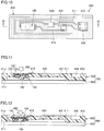
- FIG. 10 is a plan view illustrating a configuration of a resin structure according to a second embodiment
- FIG. 11 is a cross-sectional view along the cross section XI-XI in FIG. 10 .
- the resin structure 600 is provided with a molded resin element 670, the push-type switch 100, and electronic components 620, 630.
- the push-type switch 100 is embedded in the molded resin elements 670 along with the electronic components 620, 630.
- the molded resin element 670 includes a beam structure 601, and a support 602 supporting the beam structure 601.
- the push-type switch 100 is embedded in the beam structure 601 of the molded resin element 670.
- the base 130 of the push-type switch 100 is embedded in the molded resin element 670 with the button unit 160 exposed therefrom.
- the molded resin element 670 is composed of a material with a relatively low elasticity (e.g., PC resin, or ABS resin).
- FIG. 12 is a cross-sectional view illustrating how the beam structure warps when the beam structure is subject to pressure in the resin structure 600.
- the resin structure 600 includes a contacting part 690, such as a battery or housing, and an electronic device 692.
Landscapes
- Engineering & Computer Science (AREA)
- Manufacturing & Machinery (AREA)
- Microelectronics & Electronic Packaging (AREA)
- Physics & Mathematics (AREA)
- Electromagnetism (AREA)
- Push-Button Switches (AREA)
- Manufacture Of Switches (AREA)
- Switch Cases, Indication, And Locking (AREA)
- Rotary Switch, Piano Key Switch, And Lever Switch (AREA)
Applications Claiming Priority (2)
| Application Number | Priority Date | Filing Date | Title |
|---|---|---|---|
| JP2016202421A JP6669034B2 (ja) | 2016-10-14 | 2016-10-14 | 樹脂構造体、電子機器、および樹脂構造体の製造方法 |
| PCT/JP2017/033673 WO2018070191A1 (ja) | 2016-10-14 | 2017-09-19 | 樹脂構造体、電子機器、および樹脂構造体の製造方法 |
Publications (3)
| Publication Number | Publication Date |
|---|---|
| EP3528271A1 true EP3528271A1 (de) | 2019-08-21 |
| EP3528271A4 EP3528271A4 (de) | 2019-12-25 |
| EP3528271B1 EP3528271B1 (de) | 2020-11-04 |
Family
ID=61905400
Family Applications (1)
| Application Number | Title | Priority Date | Filing Date |
|---|---|---|---|
| EP17861033.3A Not-in-force EP3528271B1 (de) | 2016-10-14 | 2017-09-19 | Harzstruktur, elektronische vorrichtung und herstellungsverfahren für harzstruktur |
Country Status (6)
| Country | Link |
|---|---|
| US (1) | US10734170B2 (de) |
| EP (1) | EP3528271B1 (de) |
| JP (1) | JP6669034B2 (de) |
| CN (1) | CN109690713B (de) |
| TW (1) | TWI644337B (de) |
| WO (1) | WO2018070191A1 (de) |
Families Citing this family (2)
| Publication number | Priority date | Publication date | Assignee | Title |
|---|---|---|---|---|
| JP7315775B2 (ja) * | 2020-02-17 | 2023-07-26 | アルプスアルパイン株式会社 | 電子機器 |
| DE102024137566A1 (de) * | 2024-12-13 | 2026-06-18 | ZF Automotive Safety Germany GmbH | Schalteinheit in einem fahrzeuglenkrad |
Family Cites Families (21)
| Publication number | Priority date | Publication date | Assignee | Title |
|---|---|---|---|---|
| US3830991A (en) | 1973-07-24 | 1974-08-20 | Essex International Inc | Pressure sensitive mat switch construction |
| JPS5738468Y2 (de) * | 1978-07-31 | 1982-08-24 | ||
| JP2976648B2 (ja) * | 1991-11-15 | 1999-11-10 | 松下電器産業株式会社 | プッシュスイッチ |
| JPH06349377A (ja) * | 1993-06-14 | 1994-12-22 | Kasai Kogyo Co Ltd | プッシュボタンスイッチ |
| CH689766A5 (fr) * | 1994-02-02 | 1999-10-15 | Charles Thayer | Interrupteur en forme de bande mince. |
| US5898147A (en) * | 1997-10-29 | 1999-04-27 | C & K Components, Inc. | Dual tact switch assembly |
| JP3988443B2 (ja) * | 2001-11-28 | 2007-10-10 | 豊田合成株式会社 | 自動車内装用のスイッチ内蔵樹脂成形品の製造方法 |
| JP2007305469A (ja) * | 2006-05-12 | 2007-11-22 | Alps Electric Co Ltd | 照光式入力装置 |
| JP2008273501A (ja) | 2007-04-06 | 2008-11-13 | Nippon Sheet Glass Co Ltd | モール付きガラス及びその製造方法 |
| WO2008136251A1 (ja) * | 2007-05-02 | 2008-11-13 | Murata Manufacturing Co., Ltd. | 部品内蔵モジュール及びその製造方法 |
| TWM341912U (en) * | 2007-09-21 | 2008-10-01 | Hon Hai Prec Ind Co Ltd | Button switch |
| JP5236428B2 (ja) * | 2008-10-24 | 2013-07-17 | 日本電産サンキョー株式会社 | 検出機構およびカードリーダ |
| US20120228109A1 (en) * | 2011-03-08 | 2012-09-13 | Ibiden Co., Ltd. | Sensor, keyboard and method for manufacturing sensor |
| JP5441956B2 (ja) | 2011-05-26 | 2014-03-12 | 三菱電機株式会社 | 樹脂封止形電子制御装置及びその製造方法 |
| DE102013202703B4 (de) * | 2013-02-20 | 2020-03-12 | Siemens Healthcare Gmbh | Vorrichtung und Verfahren zur Kollisionserkennung bei einem medizintechnischen Gerät |
| US20140293560A1 (en) * | 2013-03-27 | 2014-10-02 | Samsung Electro-Mechanics Co., Ltd. | Substrate embedding electronic component and method of manufacturing substrate embedding electronic component |
| JP5806700B2 (ja) * | 2013-04-18 | 2015-11-10 | ヒロセ電機株式会社 | 回路基板用電気コネクタおよび電気コネクタ組立体 |
| CN104779108B (zh) * | 2014-01-13 | 2017-11-24 | 宏达国际电子股份有限公司 | 开关结构与使用此开关结构的电子装置 |
| JP2016127143A (ja) | 2014-12-26 | 2016-07-11 | 株式会社東芝 | 電子機器 |
| KR102380304B1 (ko) * | 2015-01-23 | 2022-03-30 | 삼성전기주식회사 | 전자부품 내장 기판 및 그 제조방법 |
| CN105655175B (zh) * | 2016-03-25 | 2018-04-03 | 江苏威尔曼科技有限公司 | 一种超薄电梯按钮 |
-
2016
- 2016-10-14 JP JP2016202421A patent/JP6669034B2/ja not_active Expired - Fee Related
-
2017
- 2017-09-19 CN CN201780055117.1A patent/CN109690713B/zh not_active Expired - Fee Related
- 2017-09-19 US US16/334,076 patent/US10734170B2/en not_active Expired - Fee Related
- 2017-09-19 WO PCT/JP2017/033673 patent/WO2018070191A1/ja not_active Ceased
- 2017-09-19 EP EP17861033.3A patent/EP3528271B1/de not_active Not-in-force
- 2017-09-26 TW TW106132910A patent/TWI644337B/zh not_active IP Right Cessation
Also Published As
| Publication number | Publication date |
|---|---|
| TWI644337B (zh) | 2018-12-11 |
| US10734170B2 (en) | 2020-08-04 |
| EP3528271A4 (de) | 2019-12-25 |
| EP3528271B1 (de) | 2020-11-04 |
| TW201816818A (zh) | 2018-05-01 |
| WO2018070191A1 (ja) | 2018-04-19 |
| JP2018063900A (ja) | 2018-04-19 |
| JP6669034B2 (ja) | 2020-03-18 |
| CN109690713A (zh) | 2019-04-26 |
| US20190362912A1 (en) | 2019-11-28 |
| CN109690713B (zh) | 2020-05-26 |
Similar Documents
| Publication | Publication Date | Title |
|---|---|---|
| CN204117915U (zh) | 半蝶形组装件、拨动开关和键机构 | |
| KR100928381B1 (ko) | 가동 접점체와 이를 이용한 스위치 | |
| CN103000415B (zh) | 开关 | |
| US8610017B2 (en) | Capacitive input switch | |
| KR20050025329A (ko) | 스위치 통합 케이싱 및 이 케이싱을 가진 전자기기 | |
| CN103714998A (zh) | 开关以及开关的制造方法 | |
| EP3528271B1 (de) | Harzstruktur, elektronische vorrichtung und herstellungsverfahren für harzstruktur | |
| US7537459B2 (en) | Anisotropic conductive film | |
| CN112189246B (zh) | 推动开关 | |
| KR100921354B1 (ko) | 스위치 장치 | |
| JP2001250445A (ja) | マイクロスイッチの製造方法、マイクロスイッチモジュールおよびマイクロスイッチモジュールの組み合わせ | |
| JP6805540B2 (ja) | 板バネの固定構造及び電気接点構造の製造方法 | |
| JP2010097708A (ja) | キースイッチ及びスイッチシート | |
| KR100458968B1 (ko) | 플랙시블 피씨비형 택트 스위치 | |
| CN208608098U (zh) | 一种薄膜按键 | |
| JP2001043772A (ja) | 押釦スイッチ装置 | |
| TWI437598B (zh) | 按鍵及應用該按鍵之電子裝置 | |
| JP2007179923A (ja) | メタルドーム押さえシート及びメタルドームスイッチ | |
| JP2002329436A (ja) | 押釦スイッチ用カバー部材及びその製造方法 | |
| KR20210117834A (ko) | Pcb 일체형 smt용 돔 스위치가 구비된 인쇄회로기판 | |
| JP4400671B2 (ja) | 異方性導電フィルム | |
| JP2011058889A (ja) | 静電容量式ポインティングデバイス | |
| JP2011233383A (ja) | タクティールスイッチ |
Legal Events
| Date | Code | Title | Description |
|---|---|---|---|
| STAA | Information on the status of an ep patent application or granted ep patent |
Free format text: STATUS: THE INTERNATIONAL PUBLICATION HAS BEEN MADE |
|
| PUAI | Public reference made under article 153(3) epc to a published international application that has entered the european phase |
Free format text: ORIGINAL CODE: 0009012 |
|
| STAA | Information on the status of an ep patent application or granted ep patent |
Free format text: STATUS: REQUEST FOR EXAMINATION WAS MADE |
|
| 17P | Request for examination filed |
Effective date: 20190319 |
|
| AK | Designated contracting states |
Kind code of ref document: A1 Designated state(s): AL AT BE BG CH CY CZ DE DK EE ES FI FR GB GR HR HU IE IS IT LI LT LU LV MC MK MT NL NO PL PT RO RS SE SI SK SM TR |
|
| AX | Request for extension of the european patent |
Extension state: BA ME |
|
| RIN1 | Information on inventor provided before grant (corrected) |
Inventor name: KAWAI, WAKAHIRO |
|
| A4 | Supplementary search report drawn up and despatched |
Effective date: 20191122 |
|
| RIC1 | Information provided on ipc code assigned before grant |
Ipc: H01H 9/02 20060101AFI20191118BHEP Ipc: H01H 13/04 20060101ALI20191118BHEP Ipc: H01H 21/00 20060101ALI20191118BHEP Ipc: H01H 13/86 20060101ALI20191118BHEP Ipc: H01H 13/702 20060101ALN20191118BHEP Ipc: H01H 13/88 20060101ALI20191118BHEP Ipc: H01H 11/00 20060101ALI20191118BHEP |
|
| DAV | Request for validation of the european patent (deleted) | ||
| DAX | Request for extension of the european patent (deleted) | ||
| GRAP | Despatch of communication of intention to grant a patent |
Free format text: ORIGINAL CODE: EPIDOSNIGR1 |
|
| RIC1 | Information provided on ipc code assigned before grant |
Ipc: H01H 9/02 20060101AFI20200604BHEP Ipc: H01H 13/04 20060101ALI20200604BHEP Ipc: H01H 13/86 20060101ALI20200604BHEP Ipc: H01H 21/00 20060101ALI20200604BHEP Ipc: H01H 11/00 20060101ALI20200604BHEP Ipc: H01H 13/702 20060101ALN20200604BHEP Ipc: H01H 13/88 20060101ALI20200604BHEP |
|
| STAA | Information on the status of an ep patent application or granted ep patent |
Free format text: STATUS: GRANT OF PATENT IS INTENDED |
|
| RIC1 | Information provided on ipc code assigned before grant |
Ipc: H01H 11/00 20060101ALI20200616BHEP Ipc: H01H 9/02 20060101AFI20200616BHEP Ipc: H01H 21/00 20060101ALI20200616BHEP Ipc: H01H 13/702 20060101ALN20200616BHEP Ipc: H01H 13/86 20060101ALI20200616BHEP Ipc: H01H 13/88 20060101ALI20200616BHEP Ipc: H01H 13/04 20060101ALI20200616BHEP |
|
| RIC1 | Information provided on ipc code assigned before grant |
Ipc: H01H 11/00 20060101ALI20200624BHEP Ipc: H01H 13/04 20060101ALI20200624BHEP Ipc: H01H 9/02 20060101AFI20200624BHEP Ipc: H01H 21/00 20060101ALI20200624BHEP Ipc: H01H 13/86 20060101ALI20200624BHEP Ipc: H01H 13/702 20060101ALN20200624BHEP Ipc: H01H 13/88 20060101ALI20200624BHEP |
|
| INTG | Intention to grant announced |
Effective date: 20200709 |
|
| GRAS | Grant fee paid |
Free format text: ORIGINAL CODE: EPIDOSNIGR3 |
|
| GRAA | (expected) grant |
Free format text: ORIGINAL CODE: 0009210 |
|
| STAA | Information on the status of an ep patent application or granted ep patent |
Free format text: STATUS: THE PATENT HAS BEEN GRANTED |
|
| AK | Designated contracting states |
Kind code of ref document: B1 Designated state(s): AL AT BE BG CH CY CZ DE DK EE ES FI FR GB GR HR HU IE IS IT LI LT LU LV MC MK MT NL NO PL PT RO RS SE SI SK SM TR |
|
| REG | Reference to a national code |
Ref country code: GB Ref legal event code: FG4D |
|
| REG | Reference to a national code |
Ref country code: CH Ref legal event code: EP |
|
| REG | Reference to a national code |
Ref country code: AT Ref legal event code: REF Ref document number: 1331884 Country of ref document: AT Kind code of ref document: T Effective date: 20201115 |
|
| REG | Reference to a national code |
Ref country code: IE Ref legal event code: FG4D |
|
| REG | Reference to a national code |
Ref country code: DE Ref legal event code: R096 Ref document number: 602017027154 Country of ref document: DE |
|
| REG | Reference to a national code |
Ref country code: NL Ref legal event code: MP Effective date: 20201104 |
|
| REG | Reference to a national code |
Ref country code: AT Ref legal event code: MK05 Ref document number: 1331884 Country of ref document: AT Kind code of ref document: T Effective date: 20201104 |
|
| PG25 | Lapsed in a contracting state [announced via postgrant information from national office to epo] |
Ref country code: GR Free format text: LAPSE BECAUSE OF FAILURE TO SUBMIT A TRANSLATION OF THE DESCRIPTION OR TO PAY THE FEE WITHIN THE PRESCRIBED TIME-LIMIT Effective date: 20210205 Ref country code: NO Free format text: LAPSE BECAUSE OF FAILURE TO SUBMIT A TRANSLATION OF THE DESCRIPTION OR TO PAY THE FEE WITHIN THE PRESCRIBED TIME-LIMIT Effective date: 20210204 Ref country code: PT Free format text: LAPSE BECAUSE OF FAILURE TO SUBMIT A TRANSLATION OF THE DESCRIPTION OR TO PAY THE FEE WITHIN THE PRESCRIBED TIME-LIMIT Effective date: 20210304 Ref country code: RS Free format text: LAPSE BECAUSE OF FAILURE TO SUBMIT A TRANSLATION OF THE DESCRIPTION OR TO PAY THE FEE WITHIN THE PRESCRIBED TIME-LIMIT Effective date: 20201104 Ref country code: FI Free format text: LAPSE BECAUSE OF FAILURE TO SUBMIT A TRANSLATION OF THE DESCRIPTION OR TO PAY THE FEE WITHIN THE PRESCRIBED TIME-LIMIT Effective date: 20201104 |
|
| PG25 | Lapsed in a contracting state [announced via postgrant information from national office to epo] |
Ref country code: ES Free format text: LAPSE BECAUSE OF FAILURE TO SUBMIT A TRANSLATION OF THE DESCRIPTION OR TO PAY THE FEE WITHIN THE PRESCRIBED TIME-LIMIT Effective date: 20201104 Ref country code: AT Free format text: LAPSE BECAUSE OF FAILURE TO SUBMIT A TRANSLATION OF THE DESCRIPTION OR TO PAY THE FEE WITHIN THE PRESCRIBED TIME-LIMIT Effective date: 20201104 Ref country code: BG Free format text: LAPSE BECAUSE OF FAILURE TO SUBMIT A TRANSLATION OF THE DESCRIPTION OR TO PAY THE FEE WITHIN THE PRESCRIBED TIME-LIMIT Effective date: 20210204 Ref country code: LV Free format text: LAPSE BECAUSE OF FAILURE TO SUBMIT A TRANSLATION OF THE DESCRIPTION OR TO PAY THE FEE WITHIN THE PRESCRIBED TIME-LIMIT Effective date: 20201104 Ref country code: PL Free format text: LAPSE BECAUSE OF FAILURE TO SUBMIT A TRANSLATION OF THE DESCRIPTION OR TO PAY THE FEE WITHIN THE PRESCRIBED TIME-LIMIT Effective date: 20201104 Ref country code: IS Free format text: LAPSE BECAUSE OF FAILURE TO SUBMIT A TRANSLATION OF THE DESCRIPTION OR TO PAY THE FEE WITHIN THE PRESCRIBED TIME-LIMIT Effective date: 20210304 Ref country code: SE Free format text: LAPSE BECAUSE OF FAILURE TO SUBMIT A TRANSLATION OF THE DESCRIPTION OR TO PAY THE FEE WITHIN THE PRESCRIBED TIME-LIMIT Effective date: 20201104 |
|
| REG | Reference to a national code |
Ref country code: LT Ref legal event code: MG9D |
|
| PG25 | Lapsed in a contracting state [announced via postgrant information from national office to epo] |
Ref country code: HR Free format text: LAPSE BECAUSE OF FAILURE TO SUBMIT A TRANSLATION OF THE DESCRIPTION OR TO PAY THE FEE WITHIN THE PRESCRIBED TIME-LIMIT Effective date: 20201104 |
|
| PG25 | Lapsed in a contracting state [announced via postgrant information from national office to epo] |
Ref country code: LT Free format text: LAPSE BECAUSE OF FAILURE TO SUBMIT A TRANSLATION OF THE DESCRIPTION OR TO PAY THE FEE WITHIN THE PRESCRIBED TIME-LIMIT Effective date: 20201104 Ref country code: CZ Free format text: LAPSE BECAUSE OF FAILURE TO SUBMIT A TRANSLATION OF THE DESCRIPTION OR TO PAY THE FEE WITHIN THE PRESCRIBED TIME-LIMIT Effective date: 20201104 Ref country code: EE Free format text: LAPSE BECAUSE OF FAILURE TO SUBMIT A TRANSLATION OF THE DESCRIPTION OR TO PAY THE FEE WITHIN THE PRESCRIBED TIME-LIMIT Effective date: 20201104 Ref country code: SM Free format text: LAPSE BECAUSE OF FAILURE TO SUBMIT A TRANSLATION OF THE DESCRIPTION OR TO PAY THE FEE WITHIN THE PRESCRIBED TIME-LIMIT Effective date: 20201104 Ref country code: RO Free format text: LAPSE BECAUSE OF FAILURE TO SUBMIT A TRANSLATION OF THE DESCRIPTION OR TO PAY THE FEE WITHIN THE PRESCRIBED TIME-LIMIT Effective date: 20201104 Ref country code: SK Free format text: LAPSE BECAUSE OF FAILURE TO SUBMIT A TRANSLATION OF THE DESCRIPTION OR TO PAY THE FEE WITHIN THE PRESCRIBED TIME-LIMIT Effective date: 20201104 |
|
| REG | Reference to a national code |
Ref country code: DE Ref legal event code: R097 Ref document number: 602017027154 Country of ref document: DE |
|
| PG25 | Lapsed in a contracting state [announced via postgrant information from national office to epo] |
Ref country code: DK Free format text: LAPSE BECAUSE OF FAILURE TO SUBMIT A TRANSLATION OF THE DESCRIPTION OR TO PAY THE FEE WITHIN THE PRESCRIBED TIME-LIMIT Effective date: 20201104 |
|
| PLBE | No opposition filed within time limit |
Free format text: ORIGINAL CODE: 0009261 |
|
| STAA | Information on the status of an ep patent application or granted ep patent |
Free format text: STATUS: NO OPPOSITION FILED WITHIN TIME LIMIT |
|
| 26N | No opposition filed |
Effective date: 20210805 |
|
| PG25 | Lapsed in a contracting state [announced via postgrant information from national office to epo] |
Ref country code: NL Free format text: LAPSE BECAUSE OF FAILURE TO SUBMIT A TRANSLATION OF THE DESCRIPTION OR TO PAY THE FEE WITHIN THE PRESCRIBED TIME-LIMIT Effective date: 20201104 Ref country code: AL Free format text: LAPSE BECAUSE OF FAILURE TO SUBMIT A TRANSLATION OF THE DESCRIPTION OR TO PAY THE FEE WITHIN THE PRESCRIBED TIME-LIMIT Effective date: 20201104 Ref country code: IT Free format text: LAPSE BECAUSE OF FAILURE TO SUBMIT A TRANSLATION OF THE DESCRIPTION OR TO PAY THE FEE WITHIN THE PRESCRIBED TIME-LIMIT Effective date: 20201104 |
|
| PGFP | Annual fee paid to national office [announced via postgrant information from national office to epo] |
Ref country code: FR Payment date: 20210812 Year of fee payment: 5 |
|
| PG25 | Lapsed in a contracting state [announced via postgrant information from national office to epo] |
Ref country code: SI Free format text: LAPSE BECAUSE OF FAILURE TO SUBMIT A TRANSLATION OF THE DESCRIPTION OR TO PAY THE FEE WITHIN THE PRESCRIBED TIME-LIMIT Effective date: 20201104 |
|
| PGFP | Annual fee paid to national office [announced via postgrant information from national office to epo] |
Ref country code: GB Payment date: 20210811 Year of fee payment: 5 |
|
| REG | Reference to a national code |
Ref country code: CH Ref legal event code: PL |
|
| REG | Reference to a national code |
Ref country code: BE Ref legal event code: MM Effective date: 20210930 |
|
| PG25 | Lapsed in a contracting state [announced via postgrant information from national office to epo] |
Ref country code: IS Free format text: LAPSE BECAUSE OF FAILURE TO SUBMIT A TRANSLATION OF THE DESCRIPTION OR TO PAY THE FEE WITHIN THE PRESCRIBED TIME-LIMIT Effective date: 20210304 Ref country code: MC Free format text: LAPSE BECAUSE OF FAILURE TO SUBMIT A TRANSLATION OF THE DESCRIPTION OR TO PAY THE FEE WITHIN THE PRESCRIBED TIME-LIMIT Effective date: 20201104 |
|
| PG25 | Lapsed in a contracting state [announced via postgrant information from national office to epo] |
Ref country code: LU Free format text: LAPSE BECAUSE OF NON-PAYMENT OF DUE FEES Effective date: 20210919 Ref country code: IE Free format text: LAPSE BECAUSE OF NON-PAYMENT OF DUE FEES Effective date: 20210919 Ref country code: BE Free format text: LAPSE BECAUSE OF NON-PAYMENT OF DUE FEES Effective date: 20210930 |
|
| PG25 | Lapsed in a contracting state [announced via postgrant information from national office to epo] |
Ref country code: LI Free format text: LAPSE BECAUSE OF NON-PAYMENT OF DUE FEES Effective date: 20210930 Ref country code: CH Free format text: LAPSE BECAUSE OF NON-PAYMENT OF DUE FEES Effective date: 20210930 |
|
| PGFP | Annual fee paid to national office [announced via postgrant information from national office to epo] |
Ref country code: DE Payment date: 20220621 Year of fee payment: 6 |
|
| GBPC | Gb: european patent ceased through non-payment of renewal fee |
Effective date: 20220919 |
|
| PG25 | Lapsed in a contracting state [announced via postgrant information from national office to epo] |
Ref country code: CY Free format text: LAPSE BECAUSE OF FAILURE TO SUBMIT A TRANSLATION OF THE DESCRIPTION OR TO PAY THE FEE WITHIN THE PRESCRIBED TIME-LIMIT Effective date: 20201104 |
|
| PG25 | Lapsed in a contracting state [announced via postgrant information from national office to epo] |
Ref country code: HU Free format text: LAPSE BECAUSE OF FAILURE TO SUBMIT A TRANSLATION OF THE DESCRIPTION OR TO PAY THE FEE WITHIN THE PRESCRIBED TIME-LIMIT; INVALID AB INITIO Effective date: 20170919 Ref country code: FR Free format text: LAPSE BECAUSE OF NON-PAYMENT OF DUE FEES Effective date: 20220930 |
|
| PG25 | Lapsed in a contracting state [announced via postgrant information from national office to epo] |
Ref country code: GB Free format text: LAPSE BECAUSE OF NON-PAYMENT OF DUE FEES Effective date: 20220919 |
|
| REG | Reference to a national code |
Ref country code: DE Ref legal event code: R119 Ref document number: 602017027154 Country of ref document: DE |
|
| PG25 | Lapsed in a contracting state [announced via postgrant information from national office to epo] |
Ref country code: MK Free format text: LAPSE BECAUSE OF FAILURE TO SUBMIT A TRANSLATION OF THE DESCRIPTION OR TO PAY THE FEE WITHIN THE PRESCRIBED TIME-LIMIT Effective date: 20201104 |
|
| PG25 | Lapsed in a contracting state [announced via postgrant information from national office to epo] |
Ref country code: TR Free format text: LAPSE BECAUSE OF FAILURE TO SUBMIT A TRANSLATION OF THE DESCRIPTION OR TO PAY THE FEE WITHIN THE PRESCRIBED TIME-LIMIT Effective date: 20201104 |
|
| PG25 | Lapsed in a contracting state [announced via postgrant information from national office to epo] |
Ref country code: DE Free format text: LAPSE BECAUSE OF NON-PAYMENT OF DUE FEES Effective date: 20240403 |
|
| PG25 | Lapsed in a contracting state [announced via postgrant information from national office to epo] |
Ref country code: MT Free format text: LAPSE BECAUSE OF FAILURE TO SUBMIT A TRANSLATION OF THE DESCRIPTION OR TO PAY THE FEE WITHIN THE PRESCRIBED TIME-LIMIT Effective date: 20201104 |