EP3514842A2 - Anzeigevorrichtung - Google Patents
Anzeigevorrichtung Download PDFInfo
- Publication number
- EP3514842A2 EP3514842A2 EP18211295.3A EP18211295A EP3514842A2 EP 3514842 A2 EP3514842 A2 EP 3514842A2 EP 18211295 A EP18211295 A EP 18211295A EP 3514842 A2 EP3514842 A2 EP 3514842A2
- Authority
- EP
- European Patent Office
- Prior art keywords
- layer
- top surface
- light
- display device
- emitting unit
- Prior art date
- Legal status (The legal status is an assumption and is not a legal conclusion. Google has not performed a legal analysis and makes no representation as to the accuracy of the status listed.)
- Granted
Links
Images








Classifications
-
- H—ELECTRICITY
- H10—SEMICONDUCTOR DEVICES; ELECTRIC SOLID-STATE DEVICES NOT OTHERWISE PROVIDED FOR
- H10D—INORGANIC ELECTRIC SEMICONDUCTOR DEVICES
- H10D86/00—Integrated devices formed in or on insulating or conducting substrates, e.g. formed in silicon-on-insulator [SOI] substrates or on stainless steel or glass substrates
- H10D86/40—Integrated devices formed in or on insulating or conducting substrates, e.g. formed in silicon-on-insulator [SOI] substrates or on stainless steel or glass substrates characterised by multiple TFTs
-
- H—ELECTRICITY
- H10—SEMICONDUCTOR DEVICES; ELECTRIC SOLID-STATE DEVICES NOT OTHERWISE PROVIDED FOR
- H10D—INORGANIC ELECTRIC SEMICONDUCTOR DEVICES
- H10D86/00—Integrated devices formed in or on insulating or conducting substrates, e.g. formed in silicon-on-insulator [SOI] substrates or on stainless steel or glass substrates
- H10D86/40—Integrated devices formed in or on insulating or conducting substrates, e.g. formed in silicon-on-insulator [SOI] substrates or on stainless steel or glass substrates characterised by multiple TFTs
- H10D86/441—Interconnections, e.g. scanning lines
-
- H—ELECTRICITY
- H10—SEMICONDUCTOR DEVICES; ELECTRIC SOLID-STATE DEVICES NOT OTHERWISE PROVIDED FOR
- H10D—INORGANIC ELECTRIC SEMICONDUCTOR DEVICES
- H10D86/00—Integrated devices formed in or on insulating or conducting substrates, e.g. formed in silicon-on-insulator [SOI] substrates or on stainless steel or glass substrates
- H10D86/40—Integrated devices formed in or on insulating or conducting substrates, e.g. formed in silicon-on-insulator [SOI] substrates or on stainless steel or glass substrates characterised by multiple TFTs
- H10D86/60—Integrated devices formed in or on insulating or conducting substrates, e.g. formed in silicon-on-insulator [SOI] substrates or on stainless steel or glass substrates characterised by multiple TFTs wherein the TFTs are in active matrices
-
- H—ELECTRICITY
- H10—SEMICONDUCTOR DEVICES; ELECTRIC SOLID-STATE DEVICES NOT OTHERWISE PROVIDED FOR
- H10H—INORGANIC LIGHT-EMITTING SEMICONDUCTOR DEVICES HAVING POTENTIAL BARRIERS
- H10H20/00—Individual inorganic light-emitting semiconductor devices having potential barriers, e.g. light-emitting diodes [LED]
- H10H20/80—Constructional details
- H10H20/81—Bodies
- H10H20/811—Bodies having quantum effect structures or superlattices, e.g. tunnel junctions
- H10H20/812—Bodies having quantum effect structures or superlattices, e.g. tunnel junctions within the light-emitting regions, e.g. having quantum confinement structures
-
- H—ELECTRICITY
- H10—SEMICONDUCTOR DEVICES; ELECTRIC SOLID-STATE DEVICES NOT OTHERWISE PROVIDED FOR
- H10H—INORGANIC LIGHT-EMITTING SEMICONDUCTOR DEVICES HAVING POTENTIAL BARRIERS
- H10H20/00—Individual inorganic light-emitting semiconductor devices having potential barriers, e.g. light-emitting diodes [LED]
- H10H20/80—Constructional details
- H10H20/81—Bodies
- H10H20/822—Materials of the light-emitting regions
- H10H20/824—Materials of the light-emitting regions comprising only Group III-V materials, e.g. GaP
- H10H20/825—Materials of the light-emitting regions comprising only Group III-V materials, e.g. GaP containing nitrogen, e.g. GaN
-
- H—ELECTRICITY
- H10—SEMICONDUCTOR DEVICES; ELECTRIC SOLID-STATE DEVICES NOT OTHERWISE PROVIDED FOR
- H10H—INORGANIC LIGHT-EMITTING SEMICONDUCTOR DEVICES HAVING POTENTIAL BARRIERS
- H10H20/00—Individual inorganic light-emitting semiconductor devices having potential barriers, e.g. light-emitting diodes [LED]
- H10H20/80—Constructional details
- H10H20/84—Coatings, e.g. passivation layers or antireflective coatings
-
- H—ELECTRICITY
- H10—SEMICONDUCTOR DEVICES; ELECTRIC SOLID-STATE DEVICES NOT OTHERWISE PROVIDED FOR
- H10H—INORGANIC LIGHT-EMITTING SEMICONDUCTOR DEVICES HAVING POTENTIAL BARRIERS
- H10H20/00—Individual inorganic light-emitting semiconductor devices having potential barriers, e.g. light-emitting diodes [LED]
- H10H20/80—Constructional details
- H10H20/85—Packages
- H10H20/851—Wavelength conversion means
- H10H20/8514—Wavelength conversion means characterised by their shape, e.g. plate or foil
-
- H—ELECTRICITY
- H10—SEMICONDUCTOR DEVICES; ELECTRIC SOLID-STATE DEVICES NOT OTHERWISE PROVIDED FOR
- H10H—INORGANIC LIGHT-EMITTING SEMICONDUCTOR DEVICES HAVING POTENTIAL BARRIERS
- H10H20/00—Individual inorganic light-emitting semiconductor devices having potential barriers, e.g. light-emitting diodes [LED]
- H10H20/80—Constructional details
- H10H20/85—Packages
- H10H20/852—Encapsulations
- H10H20/853—Encapsulations characterised by their shape
-
- H—ELECTRICITY
- H10—SEMICONDUCTOR DEVICES; ELECTRIC SOLID-STATE DEVICES NOT OTHERWISE PROVIDED FOR
- H10H—INORGANIC LIGHT-EMITTING SEMICONDUCTOR DEVICES HAVING POTENTIAL BARRIERS
- H10H20/00—Individual inorganic light-emitting semiconductor devices having potential barriers, e.g. light-emitting diodes [LED]
- H10H20/80—Constructional details
- H10H20/85—Packages
- H10H20/855—Optical field-shaping means, e.g. lenses
- H10H20/856—Reflecting means
-
- H—ELECTRICITY
- H10—SEMICONDUCTOR DEVICES; ELECTRIC SOLID-STATE DEVICES NOT OTHERWISE PROVIDED FOR
- H10H—INORGANIC LIGHT-EMITTING SEMICONDUCTOR DEVICES HAVING POTENTIAL BARRIERS
- H10H20/00—Individual inorganic light-emitting semiconductor devices having potential barriers, e.g. light-emitting diodes [LED]
- H10H20/80—Constructional details
- H10H20/85—Packages
- H10H20/857—Interconnections, e.g. lead-frames, bond wires or solder balls
-
- H—ELECTRICITY
- H10—SEMICONDUCTOR DEVICES; ELECTRIC SOLID-STATE DEVICES NOT OTHERWISE PROVIDED FOR
- H10W—GENERIC PACKAGES, INTERCONNECTIONS, CONNECTORS OR OTHER CONSTRUCTIONAL DETAILS OF DEVICES COVERED BY CLASS H10
- H10W90/00—Package configurations
-
- H—ELECTRICITY
- H10—SEMICONDUCTOR DEVICES; ELECTRIC SOLID-STATE DEVICES NOT OTHERWISE PROVIDED FOR
- H10H—INORGANIC LIGHT-EMITTING SEMICONDUCTOR DEVICES HAVING POTENTIAL BARRIERS
- H10H20/00—Individual inorganic light-emitting semiconductor devices having potential barriers, e.g. light-emitting diodes [LED]
- H10H20/01—Manufacture or treatment
- H10H20/034—Manufacture or treatment of coatings
-
- H—ELECTRICITY
- H10—SEMICONDUCTOR DEVICES; ELECTRIC SOLID-STATE DEVICES NOT OTHERWISE PROVIDED FOR
- H10H—INORGANIC LIGHT-EMITTING SEMICONDUCTOR DEVICES HAVING POTENTIAL BARRIERS
- H10H20/00—Individual inorganic light-emitting semiconductor devices having potential barriers, e.g. light-emitting diodes [LED]
- H10H20/80—Constructional details
- H10H20/85—Packages
- H10H20/8506—Containers
-
- H—ELECTRICITY
- H10—SEMICONDUCTOR DEVICES; ELECTRIC SOLID-STATE DEVICES NOT OTHERWISE PROVIDED FOR
- H10H—INORGANIC LIGHT-EMITTING SEMICONDUCTOR DEVICES HAVING POTENTIAL BARRIERS
- H10H20/00—Individual inorganic light-emitting semiconductor devices having potential barriers, e.g. light-emitting diodes [LED]
- H10H20/80—Constructional details
- H10H20/85—Packages
- H10H20/851—Wavelength conversion means
- H10H20/8515—Wavelength conversion means not being in contact with the bodies
-
- H—ELECTRICITY
- H10—SEMICONDUCTOR DEVICES; ELECTRIC SOLID-STATE DEVICES NOT OTHERWISE PROVIDED FOR
- H10W—GENERIC PACKAGES, INTERCONNECTIONS, CONNECTORS OR OTHER CONSTRUCTIONAL DETAILS OF DEVICES COVERED BY CLASS H10
- H10W72/00—Interconnections or connectors in packages
- H10W72/20—Bump connectors, e.g. solder bumps or copper pillars; Dummy bumps; Thermal bumps
-
- H—ELECTRICITY
- H10—SEMICONDUCTOR DEVICES; ELECTRIC SOLID-STATE DEVICES NOT OTHERWISE PROVIDED FOR
- H10W—GENERIC PACKAGES, INTERCONNECTIONS, CONNECTORS OR OTHER CONSTRUCTIONAL DETAILS OF DEVICES COVERED BY CLASS H10
- H10W74/00—Encapsulations, e.g. protective coatings
- H10W74/10—Encapsulations, e.g. protective coatings characterised by their shape or disposition
- H10W74/131—Encapsulations, e.g. protective coatings characterised by their shape or disposition the semiconductor body being only partially enclosed
- H10W74/141—Encapsulations, e.g. protective coatings characterised by their shape or disposition the semiconductor body being only partially enclosed the encapsulations being on at least the sidewalls of the semiconductor body
-
- H—ELECTRICITY
- H10—SEMICONDUCTOR DEVICES; ELECTRIC SOLID-STATE DEVICES NOT OTHERWISE PROVIDED FOR
- H10W—GENERIC PACKAGES, INTERCONNECTIONS, CONNECTORS OR OTHER CONSTRUCTIONAL DETAILS OF DEVICES COVERED BY CLASS H10
- H10W90/00—Package configurations
- H10W90/701—Package configurations characterised by the relative positions of pads or connectors relative to package parts
- H10W90/721—Package configurations characterised by the relative positions of pads or connectors relative to package parts of bump connectors
- H10W90/724—Package configurations characterised by the relative positions of pads or connectors relative to package parts of bump connectors between a chip and a stacked insulating package substrate, interposer or RDL
Definitions
- the present disclosure relates to a display device.
- the disclosure in particular relates to a protective layer of the display device.
- LEDs Light-emitting diodes
- GaN gallium nitride
- Current GaN-based LED devices are prepared by heteroepitaxial growth techniques on substrate materials.
- a typical wafer level LED device structure may include a lower n-doped GaN layer formed over a sapphire substrate, a single quantum well (SQW) or multiple quantum well (MWQ), and an upper p-doped GaN layer.
- Micro-LED technology is an emerging flat panel display technology.
- Micro LED displays drives an array of addressed micro LEDs.
- micro LEDs are formed and diced into several micro LED dies (e.g., micro-lighting dies).
- the driving circuits and related circuits are formed on the glass substrate to provide an array substrate (e.g., TFT array substrate), and the micro LED dies are then mounted on the array substrate.
- array substrate e.g., TFT array substrate
- Bare dies are commonly used in micro LEDs, wherein the bare dies are surrounded by a protective layer such as an anisotropic conductive film (ACF) layer.
- An ACF layer may serve as a conductive route between the electrode of micro LED and the TFT array substrate.
- the top surface of an ACF layer is level with that of a micro LED so as to provide protection.
- conductive particles having varying sizes in the ACF layer may also lead to poor conductivity or poor reflectivity.
- a display device in accordance with some embodiments of the present disclosure, includes a substrate, a driving circuit disposed on the substrate, and a light-emitting unit disposed on the driving circuit and electrically connected to the driving circuit.
- the light-emitting unit includes a first semiconductor layer, a quantum well layer disposed on the first semiconductor layer and a second semiconductor layer disposed on the quantum well layer.
- the second semiconductor layer includes a first top surface.
- the display device also includes a first protective layer disposed on the driving circuit and adjacent to the light-emitting unit.
- the first protective layer includes a second top surface and a plurality of conductive elements formed therein. The elevation of the first top surface is higher than the elevation of the second top surface.
- a display device in accordance with some embodiments of the present disclosure, includes a substrate, a driving circuit disposed on the substrate, an insulating layer disposed on the driving circuit, and a light-emitting unit disposed on the insulating layer and electrically connected to the driving circuit.
- the light-emitting unit includes a first semiconductor layer, a quantum well layer disposed on the first semiconductor layer, and a second semiconductor layer disposed on the quantum well layer.
- the second semiconductor layer includes a first top surface.
- the display device also includes a first protective layer disposed on the insulating layer and adjacent to the light-emitting unit.
- the first protective layer includes a second top surface and a plurality of conductive elements formed therein. The elevation of the first top surface is higher than the elevation of the second top surface.
- first material layer disposed on/over a second material layer may indicate the direct contact of the first material layer and the second material layer, or it may indicate a non-contact state with one or more intermediate layers between the first material layer and the second material layer. In the above situation, the first material layer may not be in direct contact with the second material layer.
- a layer overlying another layer may indicate that the layer is in direct contact with the other layer, or that the layer is not in direct contact with the other layer, there being one or more intermediate layers disposed between the layer and the other layer.
- first, second, third etc. may be used herein to describe various elements, components, regions, layers, portions and/or sections, these elements, components, regions, layers, portions and/or sections should not be limited by these terms. These terms are only used to distinguish one element, component, region, layer, portion or section from another region, layer or section. Thus, a first element, component, region, layer, portion or section discussed below could be termed a second element, component, region, layer, portion or section without departing from the teachings of the present disclosure.
- the terms “about” and “substantially” typically mean +/- 20% of the stated value, more typically +/- 10% of the stated value, more typically +/- 5% of the stated value, more typically +/- 3% of the stated value, more typically +/- 2% of the stated value, more typically +/- 1% of the stated value and even more typically +/- 0.5% of the stated value.
- the stated value of the present disclosure is an approximate value. When there is no specific description, the stated value includes the meaning of "about” or “substantially”.
- attachments, coupling and the like refer to a relationship wherein structures are secured or attached to one another either directly or indirectly through intervening structures, as well as both movable or rigid attachments or relationships, unless expressly described otherwise.
- elevation used herein means the distance from a substrate to a target surface.
- the term “elevation” may refer to the distance from a substantially planar region of a substrate to a target surface.
- an evaluation may refer to the distance from the bottom surface of a substrate to a target surface.
- the display device provided in the present disclosure includes a protective layer having the elevation that is lower than the elevation of the upper semiconductor layer of the light-emitting unit (e.g., LED, micro LED and so on). In this case, less material is required for the protective layer compared to general display devices where the elevation of the protective layer is level with that of the upper semiconductor layer. In addition, there will be more space for the wavelength conversion layer, which is disposed over the protective layer, to fill in.
- the display device includes the protective layer having the elevation that is higher than the elevation of the quantum well of the light-emitting unit so as to prevent moisture and oxygen from damaging the quantum well. Furthermore, the protective layer of such a design may also prevent shorts or increase the reflectivity.
- the display device includes a buffer layer disposed between the light emitting unit and the wavelength conversion layer so that the wavelength conversion layer may be unaffected by the current or heat produced by the light emitting-unit.
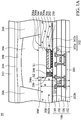
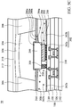
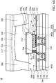
- Fig. 1A illustrates a cross-sectional view of the display device 10 in accordance with some embodiments of the present disclosure. It should be understood that additional features may be added to the display device in some embodiments of the present disclosure. In another embodiment of the present disclosure, some of the features described below may be replaced or eliminated.
- the display device 10 may include a driving substrate 100, a light-emitting unit 200 and a first protective layer 300.
- the driving substrate 100 may include a substrate 102, a driving circuit 104, a gate dielectric layer 106, a first insulating layer 108 and a second insulating layer 110.
- the driving substrate 100 may serve as a switch of the light-emitting unit 200.
- the driving circuit 104 is disposed on the substrate 102.
- the substrate 102 may include, but is not limited to, glass, quartz, sapphire, polycarbonate (PC), polyimide (PI), polyethylene terephthalate (PET), rubbers, glass fibers, other polymer materials, any other suitable substrate material, or a combination thereof.
- the substrate 102 may be made of a metal-glass fiber composite plate, a metal-ceramic composite plate, a printed circuit board, or any other suitable material, but it is not limited thereto.
- the driving circuit 104 in some embodiments as illustrated in figures is an active driving circuit including thin-film transistors (TFT), the driving circuit 104 may be a passive driving circuit in accordance with another embodiment.
- TFT thin-film transistors
- the driving circuit 104 may be controlled by an IC or a microchip.
- the driving circuit 104 may include the conductive layer, the insulating layer and the active layer, which serve as a TFT.
- the active layer may include semiconductor materials such as amorphous silicon, polysilicon or metal oxide.
- the active layer may include a pair of source/drain regions doped with suitable dopants and an undoped channel region formed between the source/drain regions.
- the gate dielectric layer 106, the first insulating layer 108 and the second insulating layer 110 are sequentially disposed on the substrate 102.
- the driving circuit 104 may be surrounded by the gate dielectric layer 106, the first insulating layer 108 and the second insulating layer 110.
- the material of the gate dielectric layer 106 may include silicon oxide, silicon nitride, silicon oxynitride, high-k dielectric material, any other suitable dielectric material, or a combination thereof.
- the high-k dielectric material may include, but is not limited to, metal oxide, metal nitride, metal silicide, transition metal oxide, transition metal nitride, transition metal silicide, metal oxynitride, metal aluminate, zirconium silicate, zirconium aluminate.
- the materials of the first insulating layer 108 or the second insulating layer 110 may be formed of an organic material, an inorganic material or a combination thereof.
- the organic material may include, but is not limited to, an acrylic or methacrylic organic compound, isoprene compound, phenol-formaldehyde resin, benzocyclobutene (BCB), PECB (perfluorocyclobutane) or a combination thereof.
- the inorganic material may include, but is not limited to, silicon nitride, silicon oxide, or silicon oxynitride or a combination thereof.
- the gate dielectric layer 106, the first insulating layer 108 or the second insulating layer 110 may be formed by using chemical vapor deposition or spin-on coating.
- the chemical vapor deposition may include, but is not limited to, low-pressure chemical vapor deposition (LPCVD), low-temperature chemical vapor deposition (LTCVD), rapid thermal chemical vapor deposition (RTCVD), plasma enhanced chemical vapor deposition (PECVD), atomic layer deposition (ALD), or any other suitable method.
- LPCVD low-pressure chemical vapor deposition
- LTCVD low-temperature chemical vapor deposition
- RTCVD rapid thermal chemical vapor deposition
- PECVD plasma enhanced chemical vapor deposition
- ALD atomic layer deposition
- the light-emitting unit 200 may be disposed on the driving substrate 100.
- the light-emitting unit 200 may be disposed on the driving circuit 104 and electrically connected to the driving circuit 104.
- the light-emitting unit 200 may be coupled to the driving circuit 104 through the vias and the pads.
- the light-emitting unit 200 may include a first semiconductor layer 202, a quantum well layer 204 disposed on the first semiconductor layer 202 and a second semiconductor layer 206 disposed on the quantum well layer 204.
- the light-emitting unit 202 may include LED or micro LED.
- the cross-sectional area of the light emitting unit 200 may have a length of about 1 ⁇ m to about 150 ⁇ m and may have a width ranging from about 1 ⁇ m to about 150 ⁇ m. In some embodiments, the light emitting unit 200 may have a size ranging from about 1 ⁇ m x 1 ⁇ m x 1 ⁇ m to about 150 ⁇ m x 150 ⁇ m x 150 ⁇ m.
- the first semiconductor layer 202 may be formed of the III-V compounds having dopants of the first conductivity type, e.g. gallium nitride having p-type conductivity (p-GaN).
- the quantum well layer 204 may include a homogeneous interface, a heterogeneous interface, a single quantum well (SQW) or a multiple quantum well (MQW).
- the material of the quantum well layer 204 may include, but is not limited to, indium gallium nitride, a gallium nitride or a combination thereof.
- the second semiconductor layer 206 may be formed of the III-V compounds having dopants of the second conductivity type, e.g. gallium nitride having n-type conductivity (n-GaN).
- the above III-V compounds may include, but is not limited to, indium nitride (InN), aluminum nitride (AlN), indium gallium nitride (InGaN), aluminum gallium nitride (AlGaN), aluminum indium gallium nitride (AlGaInN) or a combination thereof.
- the first semiconductor layer 202, the quantum well layer 204 or the second semiconductor layer 206 may be formed by using an epitaxial growth process.
- MOCVD metal organic chemical vapor deposition
- MBE molecular beam epitaxy
- HVPE hydride vapor phase epitaxy
- LPE liquid phase epitaxy
- the light-emitting unit 200 may further include a first electrode 208 and a second electrode 210.
- the first electrode 208 and the second electrode 210 may serve as the n-electrode and p-electrode of the light-emitting unit 200.
- the first electrode 208 and/or the second electrode 210 may be formed of metallic conductive materials, transparent conductive materials or a combination thereof.
- the metallic conductive material may include, but is not limited to, copper, aluminum, tungsten, titanium, gold, platinum, nickel, copper alloys, aluminum alloys, tungsten alloys, titanium alloys, gold alloys, platinum alloys, nickel alloys, any other suitable metallic conductive materials, or a combination thereof.
- the transparent conductive material may include transparent conductive oxides (TCO).
- TCO transparent conductive oxides
- the transparent conductive material may include, but is not limited to, indium tin oxide (ITO), tin oxide (SnO), zinc oxide (ZnO), indium zinc oxide (IZO), indium gallium zinc oxide (IGZO), indium tin oxide (ITZO), antimony tin oxide (ATO), antimony zinc oxide (AZO), any other suitable transparent conductive materials, or a combination thereof.
- the first electrode 208 and the second electrode 210 may be formed by, but is not limited to, chemical vapor deposition, physical vapor deposition, electroplating process, electroless plating process, any other suitable processes, or a combination thereof.
- the chemical vapor deposition may include, but is not limited to, low-pressure chemical vapor deposition (LPCVD), low-temperature chemical vapor deposition (LTCVD), rapid thermal chemical vapor deposition (RTCVD), plasma enhanced chemical vapor deposition (PECVD), atomic layer deposition (ALD), or any other suitable method.
- the physical vapor deposition may include, but is not limited to, sputtering, evaporation, pulsed laser deposition (PLD), or any other suitable method.
- the first protective layer 300 is disposed on the driving substrate 100 and adjacent to light-emitting unit 200. In other words, the light-emitting unit 200 is surrounded by the first protective layer 300.
- the first protective layer 300 may prevent moisture or oxygen from damaging the quantum well layer 204 of the light-emitting unit 200.
- the first protective layer 300 may be transparent or semi-transparent to the visible wavelength so as to not significantly degrade the light extraction efficiency of the display device.
- the first protective layer 300 may be formed of organic materials or inorganic materials.
- the inorganic material may include, but is not limited to, silicon nitride, silicon oxide, silicon oxynitride, aluminum oxide, any other suitable protective materials, or a combination thereof.
- the organic material may include, but is not limited to, epoxy resins, acrylic resins such as polymethylmetacrylate (PMMA), benzocyclobutene (BCB), polyimide, and polyester, polydimethylsiloxane (PDMS), any other suitable protective materials, or a combination thereof.
- the first protective layer 300 may be formed by using chemical vapor deposition (CVD), spin-on coating or printing.
- the chemical vapor deposition may include, but is not limited to, low-pressure chemical vapor deposition (LPCVD), low-temperature chemical vapor deposition (LTCVD), rapid thermal chemical vapor deposition (RTCVD), plasma enhanced chemical vapor deposition (PECVD), atomic layer deposition (ALD), or any other suitable method.
- LPCVD low-pressure chemical vapor deposition
- LTCVD low-temperature chemical vapor deposition
- RTCVD rapid thermal chemical vapor deposition
- PECVD plasma enhanced chemical vapor deposition
- ALD atomic layer deposition
- the first protective layer 300 may further include a plurality of conductive elements 302 formed therein. As shown in Fig. 1A , some of the conductive elements 302 may be dispersed in the first protective layer 300, and some of the conductive elements 302 may be formed on the second insulating layer 110 in accordance with some embodiments of the present disclosure.
- the conductive elements 302 may be formed as a solder composition (for example: solder ball) or formed as an eutectic composition.
- the conductive elements 302 may further include the first conductive elements 302a and the second conductive elements 302b.
- the first conductive elements 302a are disposed underneath a first terminal S1 of the light-emitting unit 200.
- the first terminal S1 is opposed to a second terminal S2.
- the first terminal S1 and the second terminal S2 may refer to the bottom and the top of the light-emitting unit 200 respectively.
- the first conductive elements 302a may be disposed between the light-emitting unit 200 and the driving substrate 100. Specifically, the first conductive elements 302a may be disposed between the first electrode 208 and the second insulating layer 110 or the second electrode 210 and the second insulating layer 110. The first conductive elements 302a may be disposed between the first electrode 208 and the contact pads on the second insulating layer 110 or the second electrode 210 and the contact pads on the second insulating layer 110. In addition, the first conductive elements 302a may electrically connect the first electrode 208 or the second electrode 210 with the driving circuit 104. On the other hand, the second conductive elements 302b may be disposed in the region out of the light-emitting unit 200. The second conductive elements 302b may be dispersed in the first protective layer 300. The second conductive elements 302b also may be disposed at the bottom of the first protective layer 300.
- the conductive elements 302 may be formed of conductive materials to serve as an electrical contact of the light-emitting unit 200.
- the conductive elements 302 may also serve as reflective particles to reflect the light emitted by light-emitting unit 200.
- the conductive elements 302 may be formed of high reflective conductive materials.
- the material of the conductive element 302 may include, but is not limited to, gold, platinum, silver, copper, iron, nickel, tin, aluminum, magnesium, palladium, iridium, rhodium, ruthenium, zinc, gold alloys, platinum alloys, silver alloys, copper alloys, iron alloys, nickel alloys, tin alloys, aluminum alloys, magnesium alloys, palladium alloys, iridium alloys, rhodium alloys, ruthenium alloys, zinc alloys, any other suitable conductive materials, or a combination thereof.
- gold alloys platinum alloys, silver alloys, copper alloys, iron alloys, nickel alloys, tin alloys, aluminum alloys, magnesium alloys, palladium alloys, iridium alloys, rhodium alloys, ruthenium alloys, zinc alloys, any other suitable conductive materials, or a combination thereof.
- the second semiconductor layer 206 of the light-emitting unit 200 includes a top surface 206a.
- the first protective layer 300 includes a top surface 300a.
- the elevation E1 of the top surface 206a of the second semiconductor layer 206 is higher than the elevation E2 of the top surface 300a of the first protective layer 300.
- the term “elevation” used herein refers to the distance from the substrate 102 to a target surface. Specifically, the term “elevation” may refer to the distance from the bottom surface the substrate 102 to a target surface.
- the elevation E1 of the top surface 206a is defined as the distance from the substrate 102 to the top surface 206a.
- the elevation E1 of the top surface 206a of the second semiconductor layer 206 is higher than the elevation E2 of the top surface 300a of the first protective layer 300. In this way, less material is required to form the protective layer 300 so that the material may be saved, compared with conventional display devices where the elevation of the protective layer is substantially level with that of the upper semiconductor layer (e.g., the second semiconductor layer 206). In addition, there will be more space for the wavelength conversion layer 304 to fill in so that the optical performance of the display device may be improved.
- the difference between the elevation E1 of the second semiconductor layer 206 and the elevation E2 of the first protective layer 300 ranges from about 0.02 ⁇ m to about 5 ⁇ m, or from about 0.2 ⁇ m to about 2 ⁇ m. It should be noted that the difference between the elevation E1 and the elevation E2 should not be too small, or the space where the additional portions 304' may be filled will be reduced and thus the illumination efficiency will be decreased and the benefit of material saving may not be achieved; and the difference between the elevation E1 and the elevation E2 should not be too great, or the protecting efficiency of the first protective layer 300 will be reduced and the light-emitting unit 200 may become easily affected by the environment.
- the quantum well layer 204 of the light-emitting unit 200 includes a top surface 204a.
- the elevation E2 of the top surface 300a of the first protective layer 300 is higher than the elevation E3 of the top surface 204a of the quantum well layer 204.
- the quantum well layer 204 is embedded in the first protective layer 300. In this way, quantum well layer 204 of the light-emitting unit 200 may be fully protected by the first protective layer 300 so as to prevent moisture and oxygen from affecting or damaging the quantum well layer 204.
- the difference between the elevation E2 of the first protective layer 300 and the elevation E3 of the quantum well layer 204 ranges from about 0.1 ⁇ m to about 10 ⁇ m, or from about 1 ⁇ m to about 5 ⁇ m. It should be noted that the difference between the elevation E2 and the elevation E3 should not be too small, or the protecting efficiency of the first protective layer 300 will be reduced and the light-emitting unit 200 may become easily affected by the environment; and the difference between the elevation E2 and the elevation E3 should not be too great, or the heat capacity of the light-emitting unit 200 will be too great so that heat may be trapped in the first protective layer 300 and may result in damages to the light-emitting unit 200 or the wavelength conversion layer 304 formed thereon. In addition, if the difference between the elevation E2 and the elevation E3 is too great, the benefit of material saving also may not be achieved.
- the display device 10 include the wavelength conversion layer 304 disposed on the light-emitting unit 200 in the embodiments illustrated in FIG. 1A
- the wavelength conversion layer 304 may be simply replaced with a transparent material without the function of wavelength conversion (e.g., without phosphor particles or quantum dot materials).
- the transparent material may include, but is not limited to, a polymer or glass matrix.
- the top surface 300a of the first protective layer 300 may be disposed at any suitable position between the top surface 204a of the quantum well layer 204 and the top surface 206a of the second semiconductor layer 206 as long as the quantum well layer 204 is covered by the first protective layer 300.
- the display device 10 may further include the wavelength conversion layer 304 disposed on the light-emitting unit 200 and the first protective layer 300, and a light shielding layer 306 disposed on the first protective layer 300.
- the wavelength conversion layer 304 may be disposed between the light shielding layers 306 and cover the light-emitting unit 200.
- the light shielding layer 306 may define a subpixel region in the display device 10. Each subpixel may correspond to a light emitting unit 200. In some embodiments, each subpixel may correspond to more than one light emitting units 200.
- the wavelength conversion layer 304 includes a portion 304' that covers a portion of the sidewall 206s of the second semiconductor layer 206.
- the additional portions 304' of the wavelength conversion layer 304 may further improve the optical performance of the display device, as compared with the conventional display devices where the top surface of the protective layer is substantially level with that of the upper semiconductor layer (i.e., without the additional wavelength conversion portions).
- the wavelength conversion layer 304 may include phosphors for converting the wavelength of light generated from the light emitting unit 200.
- the wavelength conversion layer 304 may include a polymer or glass matrix and a dispersion of phosphor particles within the matrix.
- the light emission from the light emitting unit 200 may be tuned to specific colors in the color spectrum.
- the wavelength conversion layer 304 includes the phosphors for converting the light emitted from the light emitting unit 200 into red light, green light, blue light or the light of any other suitable color.
- the wavelength conversion layer 304 includes quantum dot materials.
- the quantum dot material may have a core-shell structure.
- the core may include, but is not limited to, CdSe, CdTe, CdS, ZnS, ZnSe, ZnO, ZnTe, InAs, InP, GaP, or any other suitable materials, or a combination thereof.
- the shell may include, but is not limited to, ZnS, ZnSe, GaN, GaP, or any other suitable materials, or a combination thereof.
- the wavelength conversion layer 304 as illustrated in Fig. 1A appears to have a convex top surface, the wavelength conversion layer 304 may have any other suitable shapes according to needs.
- the configuration of the light-shielding layer 306 is not limited to that as illustrated in Fig. 1A .
- the light-shielding layer 306 may also have any other suitable configurations according to needs.
- the light-shielding layer 306 disposed adjacent to the wavelength conversion layer 304 may enhance the contrast of luminance.
- the light shielding layer 306 is formed of an opaque material such as a black matrix material.
- the black matrix material may include, but is not limited to, organic resins, glass pastes, and resins or pastes including black pigments, metallic particles such as nickel, aluminum, molybdenum, and alloys thereof, metal oxide particles (e.g. chromium oxide), or metal nitride particles (e.g. chromium nitride), or any other suitable materials.
- the wavelength conversion layer 304 and the light shielding layer 306 may be formed by using chemical vapor deposition (CVD), spin-on coating or printing.
- the chemical vapor deposition may include, but is not limited to, low-pressure chemical vapor deposition (LPCVD), low-temperature chemical vapor deposition (LTCVD), rapid thermal chemical vapor deposition (RTCVD), plasma enhanced chemical vapor deposition (PECVD), atomic layer deposition (ALD), or any other suitable method.
- LPCVD low-pressure chemical vapor deposition
- LTCVD low-temperature chemical vapor deposition
- RTCVD rapid thermal chemical vapor deposition
- PECVD plasma enhanced chemical vapor deposition
- ALD atomic layer deposition
- the display device 10 may further include a second protective layer 308 covering the wavelength conversion layer 304 and the light shielding layer 306.
- the second protective layer 308 may prevent the wavelength conversion layer 304 and the light shielding layer 306 from being affected by the outer environment.
- the second protective layer 308 may be formed of organic materials or inorganic materials.
- the inorganic material may include, but is not limited to, silicon nitride, silicon oxide, silicon oxynitride, aluminum oxide, any other suitable protective materials, or a combination thereof.
- the organic material may include, but is not limited to, epoxy resins, acrylic resins such as polymethylmetacrylate (PMMA), benzocyclobutene (BCB), polyimide, and polyester, polydimethylsiloxane (PDMS), any other suitable protective materials, or a combination thereof.
- epoxy resins acrylic resins such as polymethylmetacrylate (PMMA), benzocyclobutene (BCB), polyimide, and polyester, polydimethylsiloxane (PDMS), any other suitable protective materials, or a combination thereof.
- acrylic resins such as polymethylmetacrylate (PMMA), benzocyclobutene (BCB), polyimide, and polyester, polydimethylsiloxane (PDMS), any other suitable protective materials, or a combination thereof.
- PMMA polymethylmetacrylate
- BCB benzocyclobutene
- PDMS polydimethylsiloxane
- the second protective layer 308 may be formed by using chemical vapor deposition (CVD), spin-on coating or printing.
- the chemical vapor deposition may include, but is not limited to, low-pressure chemical vapor deposition (LPCVD), low-temperature chemical vapor deposition (LTCVD), rapid thermal chemical vapor deposition (RTCVD), plasma enhanced chemical vapor deposition (PECVD), atomic layer deposition (ALD), or any other suitable method.
- LPCVD low-pressure chemical vapor deposition
- LTCVD low-temperature chemical vapor deposition
- RTCVD rapid thermal chemical vapor deposition
- PECVD plasma enhanced chemical vapor deposition
- ALD atomic layer deposition
- the display device 10 may further include an adhesive layer 310 and a cover substrate 312.
- the adhesive layer 310 may be disposed between the second protective layer 308 and the cover substrate 312 to affix the cover substrate 312 to the second protective layer 308.
- the adhesive layer 310 may be formed of any suitable adhesive material.
- the material of the cover substrate 312 may include, but is not limited to, glass, quartz, sapphire, polycarbonate (PC), polyimide (PI), polyethylene terephthalate (PET), any other suitable substrate material, or a combination thereof.
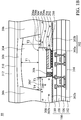
- Fig. 1B illustrates a cross-sectional view of the display device 10 in accordance with other embodiments of the present disclosure.
- the same or similar elements or layers in above and below contexts are represented by the same or similar reference numerals.
- the materials, manufacturing methods and functions of these elements or layers are the same or similar to those described above, and thus will not be repeated herein.
- the difference between the embodiments shown in Fig. 1B and Fig. 1A is that the top surface 300a of the first protective layer 300 in the embodiment shown in Fig. 1B has a concave shape while the top surface 300a of the first protective layer 300 in the embodiment shown in Fig. 1A is substantially planar.
- the wavelength conversion layer 304 located above the light-emitting unit 200 has a first thickness T1
- the wavelength conversion layer 304 including the additional portions 304' located above the protective layer 300 has a second thickness T2.
- the first thickness T1 may be defined as the maximum thickness of the wavelength conversion layer 304 that is located above the light-emitting unit 200.
- the second thickness T2 may be defined as the maximum thickness of the wavelength conversion layer 304 that is located above the protective layer 300.
- the difference between the first thickness T1 and the second thickness T2 in one subpixel may be smaller due to the concave shape of the top surface 300a, as compared with that of the substantially planar top surface 300a (as shown in Fig. 1A ).
- the third thickness T3 of the additional portions 304' that is closer to the light-emitting unit 200 may be smaller than the fourth thickness T4 of the additional portions 304' that is farther from the light-emitting unit 200 due to the concave shape of the top surface 300a.
- the concave shape of the top surface 300a may be formed due to the hydrophobic properties of the chosen materials of the first protective layer 300.
- the concave shape of the top surface 300a may be formed by a patterning process.
- the patterning process may include a photolithography process and an etching process such as a selective etching process.
- the photolithography process may include, but is not limited to, photoresist coating (e.g., spin-on coating), soft baking, hard baking, mask aligning, exposure, post-exposure baking, developing the photoresist, rinsing, drying, and other suitable processes.
- the etching process may include dry etching process or wet etching process.
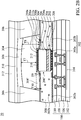
- Fig. 1C illustrates a cross-sectional view of the display device 10 in accordance with other embodiments of the present disclosure.
- the difference between the embodiments shown in Fig. 1C and Fig. 1A is that the top surface 300a of the first protective layer 300 in the embodiment shown in Fig. 1C has a convex shape while the top surface 300a of the first protective layer 300 in the embodiment shown in Fig. 1A is substantially planar.
- the fifth thickness T5 of the additional portions 304' that is closer to the light-emitting unit 200 may be greater than the sixth thickness T6 of the additional portions 304' that is farther from the light-emitting unit 200 due to the convex shape of the top surface 300a.
- the reflected light L may be concentrated to increase the illumination efficiency due to the convex surface of the top surface 300a.
- the convex shape of the top surface 300a may be formed due to the hydrophilic properties of the chosen materials of the first protective layer 300.
- the convex shape of the top surface 300a may be formed by a patterning process.
- the patterning process may include a photolithography process and an etching process such as a selective etching process.
- the photolithography process may include, but is not limited to, photoresist coating (e.g., spin-on coating), soft baking, hard baking, mask aligning, exposure, post-exposure baking, developing the photoresist, rinsing, drying, and other suitable processes.
- the etching process may include dry etching process or wet etching process.
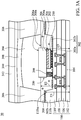
- Fig. 2A illustrates a cross-sectional view of the display device 20 in accordance with some embodiments of the present disclosure.
- the difference between the embodiments shown in Fig. 2A and Fig. 1A is that the light-emitting unit 200' in the embodiment shown in Fig. 2A is a vertical chip type light-emitting diode while the light-emitting unit 200 in the embodiment shown in Fig. 1A is a flip chip type light-emitting diode.
- the light-emitting unit 200' may be disposed on the driving circuit 104 and electrically connected to the driving circuit 104.
- the first electrode 208 of the light-emitting unit 200' is disposed on the conductive elements 302 and may serve as a bottom electrode of the light-emitting unit 200'.
- the first semiconductor layer 202, the quantum well layer 204 and the second semiconductor layer 206 are sequentially stacked on the first electrode 208.
- the second electrode 210 is disposed on the second semiconductor layer 206 and may serve as a top electrode of the light-emitting unit 200.
- the light-emitting unit 200' may further include a contact layer 212 disposed on the second electrode 210 and the first protective layer 300.
- the contact layer 212 may serve as an electrical contact of the light-emitting unit 200'.
- the contact layer 212 may be conformally formed over the second electrode 210 and the first protective layer 300.
- the contact layer 212 may couple to the circuit from different array or to the circuit outside the panel.
- the material of the contact layer 212 may include transparent conductive oxides (TCO).
- TCO transparent conductive oxides
- the transparent conductive material may include, but is not limited to, indium tin oxide (ITO), tin oxide (SnO), zinc oxide (ZnO), indium zinc oxide (IZO), indium gallium zinc oxide (IGZO), indium tin oxide (ITZO), antimony tin oxide (ATO), antimony zinc oxide (AZO), any other suitable transparent conductive materials, or a combination thereof.
- the contact layer 212 may be formed by using chemical vapor deposition (CVD) or spin-on coating.
- the chemical vapor deposition may include, but is not limited to, low-pressure chemical vapor deposition (LPCVD), low-temperature chemical vapor deposition (LTCVD), rapid thermal chemical vapor deposition (RTCVD), plasma enhanced chemical vapor deposition (PECVD), atomic layer deposition (ALD), or any other suitable method.
- LPCVD low-pressure chemical vapor deposition
- LTCVD low-temperature chemical vapor deposition
- RTCVD rapid thermal chemical vapor deposition
- PECVD plasma enhanced chemical vapor deposition
- ALD atomic layer deposition
- the elevation E1 of the top surface 206a of the second semiconductor layer 206 is higher than the elevation E2 of the top surface 300a of the first protective layer 300.
- the difference between the elevation E1 of the second semiconductor layer 206 and the elevation E2 of the first protective layer 300 ranges from about 0.02 ⁇ m to about 5 ⁇ m, or from about 0.2 ⁇ m to about 2 ⁇ m.
- the elevation E2 of the top surface 300a of the first protective layer 300 is higher than the elevation E3 of the top surface 204a of the quantum well layer 204.
- the difference between the elevation E2 of the first protective layer 300 and the elevation E3 of the quantum well layer 204 ranges from about 0.1 ⁇ m to about 10 ⁇ m, or from about 1 ⁇ m to about 5 ⁇ m.
- the second electrode 210 of the light-emitting unit 200' includes a top surface 210a.
- the elevation E4 of the top surface 210a of the second electrode 210 is also higher than the elevation E2 of the top surface 300a of the first protective layer 300.
- the difference between the elevation E4 of the second electrode 210 and the elevation E2 of the first protective layer 300 ranges from about 0.02 ⁇ m to about 5 ⁇ m, or from about 0.2 ⁇ m to about 2 ⁇ m.
- Fig. 2B illustrates a cross-sectional view of the display device 20 in accordance with other embodiments of the present disclosure.
- the difference between the embodiments shown in Fig. 2B and Fig. 2A is that the top surface 300a of the first protective layer 300 in the embodiment shown in Fig. 2B has a concave shape while the top surface 300a of the first protective layer 300 in the embodiment shown in Fig. 2A is substantially planar.
- the top surface 212a of the contact layer 212 may also has a concave shape.
- the wavelength conversion layer 304 located above the light-emitting unit 200' has a seventh thickness T7
- the wavelength conversion layer 304 including the additional portions 304' located above the protective layer 300 has an eighth thickness T8.
- the seventh thickness T7 may be defined as the maximum thickness of the wavelength conversion layer 304 that is located above both the light-emitting unit 200' and the contact layer 212.
- the eighth thickness T8 may be defined as the maximum thickness of the wavelength conversion layer 304 that is located both above the protective layer 300 and the contact layer 212.
- the difference between the seventh thickness T7 and the eighth thickness T8 in one subpixel may be smaller due to the concave shape of the top surface 300a and the top surface 212a, as compared with that of the substantially planar top surface 300a and the top surface 212a (as shown in Fig. 2A ).
- the ninth thickness T9 of the additional portions 304' that is closer to the light-emitting unit 200' may be smaller than the tenth thickness T10 of the additional portions 304' that is farther from the light-emitting unit 200' due to the concave shape of the top surface 300a and the top surface 212a.
- Fig. 2C illustrates a cross-sectional view of the display device 20 in accordance with other embodiments of the present disclosure.
- the difference between the embodiments shown in Fig. 2C and Fig. 2A is that the top surface 300a of the first protective layer 300 in the embodiment shown in Fig. 2C has a convex shape while the top surface 300a of the first protective layer 300 in the embodiment shown in Fig. 2A is substantially planar.
- the top surface 212a of the contact layer 212 may also has a convex shape.
- the eleventh thickness T11 of the additional portions 304' that is closer to the light-emitting unit 200' may be greater than the twelfth thickness T12 of the additional portions 304' that is farther from the light-emitting unit 200' due to the convex shape of the top surface 300a and the top surface 212a.
- the reflected light L may be concentrated to increase the illumination efficiency due to the convex surface of the top surface 300a and the top surface 212a.
- Fig. 3A illustrates a cross-sectional view of the display device 30 in accordance with some embodiments of the present disclosure.
- the difference between the embodiments shown in Fig. 3A and Fig. 1A is that the second insulating layer 110' in the embodiment shown in Fig. 3A further includes a bank portion 110b.
- the bank portion 110b of the second insulating layer 110' protrudes toward the light shielding layer 306.
- the bank portion 110b of the second insulating layer 110' includes a top surface 110ba.
- the elevation E5 of the top surface 110ba of the second insulating layer 110' is lower than the elevation E2 of the top surface 300a of the first protective layer 300.
- the materials of the first protective layer 300 may be conserved since the bank portions 110b of the second insulating layer 110' occupies some of the spaces that are originally to be filled in with the first protective layer 300.
- the elevation E5 of the top surface 110ba of the second insulating layer 110' may be lower or higher than the elevation E3 of the top surface 204a of the quantum well layer 204.
- the light-emitting units 200 may be disposed in the trench or the cavity defined by the bank portions 110b. In some embodiments, a plurality of light-emitting units 200 are disposed in the same trench defined by the bank portions 110b. In other embodiments, each of the light-emitting unit 200 is disposed in a cavity defined by the bank portions 110b separately. In addition, each cavity includes a plurality of light-emitting units 200 disposed therein in accordance with some embodiments.
- the bank portion 110b may be formed by performing a patterning process to the second insulating layer 110'.
- the patterning process may include a photolithography process and an etching process such as a selective etching process.
- the photolithography process may include, but is not limited to, photoresist coating (e.g., spin-on coating), soft baking, hard baking, mask aligning, exposure, post-exposure baking, developing the photoresist, rinsing, drying, and other suitable processes.
- the etching process may include dry etching process or wet etching process.
- the elevation E5 of the top surface 110ba of the second insulating layer 110' is equal to the elevation E2 of the top surface 300a of the first protective layer 300. In accordance with other embodiments of the present disclosure, the elevation E5 of the top surface 110ba of the second insulating layer 110' is higher than the elevation E2 of the top surface 300a of the first protective layer 300 (as shown in Fig. 3B ).
- the second insulating layer 110' may be a two-layered structure or multi-layers stack structure in accordance with some embodiments.
- Fig. 4 illustrates a cross-sectional view of the display device 40 in accordance with some embodiments of the present disclosure.
- the difference between the embodiments shown in Fig. 4 and Fig. 1A is that the top surface 300a of the first protective layer 300 in the embodiment shown in Fig. 4 includes a plurality of recesses 314.
- the top surface 300a of the first protective layer 300 has a pothole structure.
- the recesses 314 of the top surface 300a of the first protective layer 300 may be randomly distributed.
- the size of the recess 314 may range from about 1 nm to about 10um or from about 100nm to about 2um.
- the recesses 314 of the top surface 300a of the first protective layer 300 may prevent the reflected light from being trapped in the first protective layer 300 due to the total reflection. Accordingly, the recesses 314 of the top surface 300a may increase or improve the illumination efficiency of the display device.
- the recesses 314 of the top surface 300a may be formed by a patterning process.
- the patterning process may include a photolithography process and an etching process such as a selective etching process.
- the photolithography process may include, but is not limited to, photoresist coating (e.g., spin-on coating), soft baking, hard baking, mask aligning, exposure, post-exposure baking, developing the photoresist, rinsing, drying, and other suitable processes.
- the etching process may include dry etching process or wet etching process.
- Fig. 5A illustrates a cross-sectional view of the display device 50 in accordance with some embodiments of the present disclosure.
- the difference between the embodiments shown in Fig. 5A and Fig. 1A is that the display device 50 further includes a buffer layer 316 disposed on the light-emitting unit 200.
- the buffer layer 316 may be disposed on the light-emitting unit 200 and the first protective layer 300.
- the buffer layer 316 may be disposed between the light-emitting unit 200 and the wavelength conversion layer304.
- the buffer layer 316 may be conformally formed over the light-emitting unit 200 and the first protective layer 300.
- the buffer layer 316 may cover the sidewall 206s of the second semiconductor layer 206.
- the buffer layer 316 may be disposed between the light-emitting unit 200 and the wavelength conversion layer 304 so that the direct contact between the light-emitting unit 200 and the wavelength conversion layer 304 may be avoided.
- the wavelength conversion layer 304 may be unaffected by the current or heat produced by the light-emitting unit 200.
- the display device 50 include the wavelength conversion layer 304 disposed on the light-emitting unit 200 in the embodiments illustrated in FIG. 5A
- the wavelength conversion layer 304 may be simply replaced with a transparent material without the function of wavelength conversion (e.g., without phosphor particles or quantum dot materials).
- the transparent material may include, but is not limited to, a polymer or glass matrix.
- the buffer layer 316 may be an insulator.
- the buffer layer 316 may include organic materials and/or inorganic materials.
- the buffer layer 316 may be formed of organic insulating materials.
- the organic insulating material may include, but is not limited to, polyamide, polyethylene, polystyrene, polypropylene, polyester, polyimide, polyurethane, silicones, polyacrylate, benzo-cyclo-butene (BCB), polyvinylpyrrolidone (PVP), polyvinylfluoride (PVF), polyvinylidene fluoride (PVDF), polytetrafluoroethylene (PTFE), polymethylmetacrylate (PMMA), polydimethylsiloxane (PDMS), any other suitable organic insulating materials, or a combination thereof.
- the inorganic insulating material may include, but is not limited to, SiOx, SiNx, AlOx, any other suitable inorganic insulating materials, or
- the buffer layer 316 may be formed by using chemical vapor deposition (CVD) or spin-on coating.
- the chemical vapor deposition may include, but is not limited to, low-pressure chemical vapor deposition (LPCVD), low-temperature chemical vapor deposition (LTCVD), rapid thermal chemical vapor deposition (RTCVD), plasma enhanced chemical vapor deposition (PECVD), atomic layer deposition (ALD), or any other suitable method.
- LPCVD low-pressure chemical vapor deposition
- LTCVD low-temperature chemical vapor deposition
- RTCVD rapid thermal chemical vapor deposition
- PECVD plasma enhanced chemical vapor deposition
- ALD atomic layer deposition
- the thickness of the buffer layer 316 may not be uniform. As shown in Fig. 5A , the buffer layer 316 located above the first protective layer 300 may have a thirteenth thickness T13, and the buffer layer 316 located above the light-emitting unit 200 has a fourteenth thickness T14. In some embodiments of the present disclosure, the thirteenth thickness T13 of the buffer layer 316 is greater than the fourteenth thickness T14 of the buffer layer 316. That is, the buffer layer 316 disposed directly on the light-emitting unit 200 may be thinner than the buffer layer 316 directly disposed on the first protective layer 300.
- the difference between the thirteenth thickness T13 and the fourteenth thickness T14 may range from about 0.001um to about 5um or from about 0.05um to about 2um. In some embodiments of the present disclosure, the thirteenth thickness T13 of the buffer layer 316 may range from about 0.02 ⁇ m to about 5 ⁇ m or from about 0.1um to about 2um. In some embodiments of the present disclosure, the fourteenth thickness T14 of the buffer layer 316 may range from about 0.02 ⁇ m to about 5 ⁇ m or from about 0.1um to about 2um.
- Fig. 5B illustrates a cross-sectional view of the display device 50 in accordance with other embodiments of the present disclosure.
- the difference between the embodiments shown in Fig. 5B and Fig. 5A is that the top surface 316a of the buffer layer 316 on the first protective layer 300 in the embodiment shown in Fig. 5B has a concave shape while the top surface 316a of the buffer layer 316 on the first protective layer 300 in the embodiment shown in Fig. 5A is substantially planar.
- the top surface 316a of the buffer layer 316 on the first protective layer 300 may have a convex shape in accordance with other embodiments of the present disclosure.
- Fig. 6A illustrates a cross-sectional view of the display device 60 in accordance with other embodiments of the present disclosure.
- the difference between the embodiments shown in Fig. 6A and Fig. 5A is that the buffer layer 316' in the embodiment shown in Fig. 6A is a discontinuous structure while the buffer layer 316 in the embodiment shown in Fig. 5A is a continuous structure.
- the buffer layers 316' within different subpixels may be discontinuous. In other words, the buffer layers 316' from different subpixels may be separated. In this embodiment, a portion of the buffer layers 316' may be disposed over the light-emitting unit 200 while another portion of the buffer layers 316' may be disposed over the first protective layer 300. In particular, the buffer layers 316' may entirely cover the top surface 206a of the second semiconductor layer 206, and partially cover the top surface 300a of the first protective layer 300. In some embodiments of the present disclosure, the buffer layer 316' extends from the light-emitting unit 200 through the wavelength conversion layer 304 and to the light shielding layer 306.
- the buffer layers 316' may be formed by a patterning process.
- the patterning process may include a photolithography process and an etching process such as a selective etching process.
- the photolithography process may include, but is not limited to, photoresist coating (e.g., spin-on coating), soft baking, hard baking, mask aligning, exposure, post-exposure baking, developing the photoresist, rinsing, drying, and other suitable processes.
- the etching process may include dry etching process or wet etching process.
- Fig. 6B illustrates a cross-sectional view of the display device 60 in accordance with other embodiments of the present disclosure.
- the difference between the embodiments shown in Fig. 6B and Fig. 6A is that the buffer layer 316" in the embodiment shown in Fig. 6B does not extend to the light shielding layer 306.
- the buffer layer 316" may entirely cover the top surface 206a of the second semiconductor layer 206, and partially cover the sidewall 206s of the second semiconductor layer 206.
- the buffer layer 316" does not extend along the top surface 300a of the protective layer 300.
- the buffer layers 316" may be formed by the patterning process as described above.
- Fig. 7A illustrates a cross-sectional view of the display device 70 in accordance with some embodiments of the present disclosure.
- the difference between the embodiments shown in Fig. 7A and Fig. 2A is that the display device 70 further includes a buffer layer 316 disposed on the contact layer 212.
- the buffer layer 316 may be disposed between the contact layer 212 and the wavelength conversion layer 310.
- the buffer layer 316 may be conformally formed over the contact layer 212.
- the buffer layer 316 may be disposed between the contact layer 212 and the wavelength conversion layer 310 so that the direct contact between the contact layer 212 and the wavelength conversion layer 310 may be avoided.
- the wavelength conversion layer 310 may be unaffected by the current or heat produced by the light-emitting unit 200 including the contact layer 212.
- the thickness of the buffer layer 316 may not be uniform. As shown in Fig. 7 , the buffer layer 316 disposed directly above the light-emitting unit 200 may be thinner than the buffer layer 316 directly disposed above the first protective layer 300 in accordance with some embodiments of the present disclosure. In such a configuration, the intensity of the light emitted from the light-emitting unit 200 will not be greatly decreased since the buffer layer 316 disposed on the light-emitting unit 200 is thinner.
- Fig. 8 illustrates a cross-sectional view of the display device 80 in accordance with some embodiments of the present disclosure.
- the difference between the embodiments shown in Fig. 8 and Fig. 5A is that the top surface 316a" of the buffer layer 316 on the light-emitting unit 200 in the embodiment shown in Fig. 8 is rougher than the top surface 316a' of the buffer layer 316 on the first protective layer 300.
- the top surface 316a of the buffer layer 316 may further include the top surface 316a" that is disposed above the light-emitting unit 200 and the top surface 316a' that is disposed above the first protective layer 300 and out of the light-emitting unit 200.
- the top surface 316a" may be rougher than the top surface 316a'.
- the surface roughness of the top surface 316a' may range from about 2nm to about 30nm.
- the surface roughness of the top surface 316a" may range from about 5nm to about 100nm.
- the difference of the surface roughness between the top surface 316a" and the top surface 316a' may range from about 3nm to about 100nm. In such a configuration, the light from the light-emitting unit 200 may be emitted more uniformly so that the conversion efficiency of the wavelength conversion layer 304 may be increased.
- the rough top surface 316a" may be formed by an etching process.
- the etching process may include dry etching process or wet etching process.
- Fig. 9A illustrates a partially enlarged portion of the display device 50 in Fig. 5A .
- the conductive elements 302 may include the first conductive elements 302a and the second conductive elements 302b.
- the first conductive elements 302a may be disposed underneath the first terminal S1 of the light-emitting unit 200.
- the first conductive elements 302a may be disposed between the light-emitting unit 200 and the second insulating layer 110.
- first conductive elements 302a may be disposed between the first electrode 208 and the contact structures (e.g., the conductive pads) on the second insulating layer 110; and some of the first conductive elements 302a may be disposed between the second electrode 210 and the contact structures (e.g., the conductive pads) on the second insulating layer 110.
- the second conductive elements 302b may be disposed in the region out of the light-emitting unit 200. The second conductive elements 302b may be dispersed in the first protective layer 300 or disposed at the top surface 110a of the second insulating layer 110.
- a height-to-width ratio of the first conductive element 302a ranges from about 0.25 to about 0.75 or from about 0.4 to about 0.6.
- the height-to-width ratio of the first conductive element 302a should not be too small, or the contact yield will dramatically decrease; and the height-to-width ratio of the first conductive element 302a should not be too great, or the contact resistance will be too high due to the contact area of a single conductive element 302a is too low.
- a height-to-width ratio of the second conductive element 302b ranges from about 0.7 to about 1.3 or from about 0.8 to about 1.2.
- the height-to-width ratio of the second conductive element 302b should not be too small, or the light being reflected by the second conductive element 302b will be nonuniform; and the height-to-width ratio of the first conductive element 302a should not be too great, or the light being reflected by the second conductive element 302b will dramatically decrease.
- the height-to-width ratio used herein is measured from the cross-sectional structure obtained from the conductive element 302.
- the variation of height-to-width ratio may be from about 0% to about 5% due to the process for obtaining the cross-sectional structure.
- the "height" of the height-to-width ratio is defined as the maximum height along a first direction of a cross-sectional structure obtained from the conductive element 302.
- the "width" of the height-to-width ratio is defined as the maximum width along a second direction of a cross-sectional structure obtained from the conductive element 302. The above first direction and the second direction are orthogonal to each other.
- Fig. 9B and Fig. 9C illustrate the cross-sectional views of the first conductive elements 302a in accordance with some embodiments of the present disclosure.
- the cross-sectional structure of the exemplary first conductive element 302a has a maximum height H1 along a first direction A and a maximum width W1 along a second direction B.
- the first direction A is orthogonal to the second direction B.
- the height-to-width ratio of the first conductive element 302a is H1/W1.
- the cross-sectional structure of the first conductive element 302a may have, but is not limited to, an ellipse shape or an ellipse-like shape.
- Fig. 9D and Fig. 9E illustrate the cross-sectional views of the second conductive elements 302b in accordance with some embodiments of the present disclosure.
- the cross-sectional structure of the exemplary second conductive element 302b has a maximum height H2 along a first direction A and a maximum width W2 along a second direction B.
- the first direction A is orthogonal to the second direction B.
- the height-to-width ratio of the second conductive element 302b is H2/W2.
- the cross-sectional structure of the second conductive element 302b may have, but is not limited to, a circular shape or a circular-like shape.
- the display device provided in the present disclosure includes a protective layer having the elevation that is lower than the elevation of the upper semiconductor layer of the light-emitting unit.
- a protective layer having the elevation that is lower than the elevation of the upper semiconductor layer of the light-emitting unit.
- less material is required for the protective layer compared to general display devices where the elevation of the protective layer is level with that of the upper semiconductor layer.
- the display device includes the protective layer having the elevation that is higher than the elevation of the quantum well of the light-emitting unit so as to prevent moisture and oxygen from damaging the quantum well.
- the protective layer of such a design may also prevent shorts or increase the reflectivity.
- the display device includes a buffer layer disposed between the light emitting unit and the wavelength conversion layer so that the wavelength conversion layer may be unaffected by the current or heat produced by the light emitting-unit.
- a display device comprising: a substrate; a driving circuit disposed on the substrate; an insulating layer disposed on the driving circuit; a light-emitting unit disposed on the insulating layer and electrically connected to the driving circuit, wherein the light-emitting unit comprises:a first semiconductor layer; a quantum well layer disposed on the first semiconductor layer; anda second semiconductor layer disposed on the quantum well layer, and the second semiconductor layer comprises a first top surface; and
Landscapes
- Led Devices (AREA)
- Electroluminescent Light Sources (AREA)
- Devices For Indicating Variable Information By Combining Individual Elements (AREA)
Applications Claiming Priority (1)
| Application Number | Priority Date | Filing Date | Title |
|---|---|---|---|
| US15/855,062 US10193042B1 (en) | 2017-12-27 | 2017-12-27 | Display device |
Publications (3)
| Publication Number | Publication Date |
|---|---|
| EP3514842A2 true EP3514842A2 (de) | 2019-07-24 |
| EP3514842A3 EP3514842A3 (de) | 2019-10-02 |
| EP3514842B1 EP3514842B1 (de) | 2022-04-27 |
Family
ID=64664134
Family Applications (1)
| Application Number | Title | Priority Date | Filing Date |
|---|---|---|---|
| EP18211295.3A Active EP3514842B1 (de) | 2017-12-27 | 2018-12-10 | Anzeigevorrichtung |
Country Status (4)
| Country | Link |
|---|---|
| US (5) | US10193042B1 (de) |
| EP (1) | EP3514842B1 (de) |
| KR (2) | KR102576517B1 (de) |
| CN (2) | CN113078246B (de) |
Cited By (1)
| Publication number | Priority date | Publication date | Assignee | Title |
|---|---|---|---|---|
| EP3618113A1 (de) * | 2018-08-28 | 2020-03-04 | LG Display Co., Ltd. | Anzeigevorrichtung |
Families Citing this family (45)
| Publication number | Priority date | Publication date | Assignee | Title |
|---|---|---|---|---|
| KR102521100B1 (ko) * | 2018-01-08 | 2023-04-14 | 삼성디스플레이 주식회사 | 표시 장치 |
| US10545379B2 (en) * | 2018-02-01 | 2020-01-28 | Innolux Corporation | Display device |
| KR102786764B1 (ko) * | 2018-07-11 | 2025-03-27 | 엘지전자 주식회사 | 반도체 발광 소자를 이용한 디스플레이 장치 및 이의 제조방법 |
| KR102597018B1 (ko) * | 2018-08-23 | 2023-10-31 | 엘지디스플레이 주식회사 | 표시 장치 및 표시 장치의 제조 방법 |
| RU2696004C1 (ru) | 2018-08-29 | 2019-07-30 | Акционерное Общество "Атомэнергопроект" | Система локализации и охлаждения расплава активной зоны ядерного реактора водоводяного типа |
| CN109273479B (zh) * | 2018-09-20 | 2021-07-23 | 上海天马微电子有限公司 | 一种显示面板及其制作方法 |
| CN109791939B (zh) * | 2018-10-12 | 2023-08-08 | 京东方科技集团股份有限公司 | 微发光二极管显示面板、微发光二极管显示装置和制造微发光二极管显示面板的方法 |
| CN109496368A (zh) * | 2018-10-12 | 2019-03-19 | 京东方科技集团股份有限公司 | 微发光二极管装置及其制造方法 |
| US11424224B2 (en) * | 2019-04-24 | 2022-08-23 | Seoul Viosys Co., Ltd. | LED display panel, LED display apparatus having the same and method of fabricating the same |
| CN111916534B (zh) * | 2019-05-07 | 2022-06-21 | 錼创显示科技股份有限公司 | 微型元件 |
| TWI729389B (zh) * | 2019-05-07 | 2021-06-01 | 錼創顯示科技股份有限公司 | 微型元件 |
| US11710760B2 (en) * | 2019-06-21 | 2023-07-25 | Semiconductor Energy Laboratory Co., Ltd. | Display device, display module, electronic device, and manufacturing method of display device |
| JP7321792B2 (ja) * | 2019-06-26 | 2023-08-07 | 株式会社ジャパンディスプレイ | 異方性導電膜及び表示装置 |
| KR102793630B1 (ko) | 2019-07-02 | 2025-04-11 | 삼성전자주식회사 | 로봇청소기 스테이션 |
| CN110416248B (zh) * | 2019-08-06 | 2022-11-04 | 京东方科技集团股份有限公司 | 一种显示基板及其制备方法、显示装置 |
| CN110600589B (zh) * | 2019-08-30 | 2024-08-09 | 深圳市科创数字显示技术有限公司 | 微发光二极管显示器及其制作方法 |
| JP7617356B2 (ja) * | 2019-10-01 | 2025-01-20 | 日亜化学工業株式会社 | 画像表示装置の製造方法および画像表示装置 |
| CN110767646B (zh) * | 2019-10-31 | 2021-02-09 | 京东方科技集团股份有限公司 | 显示基板及其制造方法、显示装置 |
| JP7641724B2 (ja) * | 2019-11-12 | 2025-03-07 | 株式会社半導体エネルギー研究所 | 機能パネル、表示装置、入出力装置、情報処理装置 |
| CN112820205B (zh) * | 2019-11-15 | 2023-01-31 | 成都辰显光电有限公司 | 显示面板及其制备方法、显示装置 |
| US11610877B2 (en) * | 2019-11-21 | 2023-03-21 | Semiconductor Energy Laboratory Co., Ltd. | Functional panel, display device, input/output device, and data processing device |
| CN111048499B (zh) * | 2019-12-16 | 2022-05-13 | 业成科技(成都)有限公司 | 微发光二极管显示面板及其制备方法 |
| CN119695026A (zh) * | 2019-12-20 | 2025-03-25 | 群创光电股份有限公司 | 电子装置 |
| US11901497B2 (en) * | 2019-12-24 | 2024-02-13 | Seoul Viosys Co., Ltd. | Method of repairing light emitting device, apparatus for repairing light emitting device, and display panel having repaired light emitting device |
| CN113078179A (zh) * | 2020-01-06 | 2021-07-06 | 群创光电股份有限公司 | 电子装置 |
| CN113140664A (zh) * | 2020-01-20 | 2021-07-20 | 北京芯海视界三维科技有限公司 | 显示单元和显示器 |
| CN112968097A (zh) * | 2020-05-14 | 2021-06-15 | 重庆康佳光电技术研究院有限公司 | 一种色彩转换方法及显示器件 |
| CN113972197A (zh) * | 2020-07-23 | 2022-01-25 | 宏碁股份有限公司 | 显示装置与其制造方法 |
| KR102901863B1 (ko) * | 2020-09-03 | 2025-12-18 | 삼성디스플레이 주식회사 | 표시 장치 |
| KR102905310B1 (ko) * | 2020-09-23 | 2025-12-30 | 삼성디스플레이 주식회사 | 표시 장치 및 그의 제조 방법 |
| KR102925282B1 (ko) * | 2020-10-06 | 2026-02-09 | 삼성디스플레이 주식회사 | 발광 소자, 발광 소자의 제조 방법, 및 이를 포함하는 표시 장치 |
| KR102949495B1 (ko) * | 2020-11-30 | 2026-04-07 | 삼성디스플레이 주식회사 | 표시 장치 |
| US12206052B2 (en) * | 2020-11-30 | 2025-01-21 | Nichia Corporation | Light-emitting device and planar light source that utilizes multiple wavelength conversion layers |
| US12154936B2 (en) * | 2021-02-02 | 2024-11-26 | Samsung Electronics Co., Ltd. | Display module and manufacturing method thereof |
| CN116783640A (zh) * | 2021-03-29 | 2023-09-19 | 日亚化学工业株式会社 | 图像显示装置的制造方法和图像显示装置 |
| JP7387978B2 (ja) * | 2021-04-20 | 2023-11-29 | 日亜化学工業株式会社 | 発光装置 |
| DE102021110089A1 (de) | 2021-04-21 | 2022-10-27 | OSRAM Opto Semiconductors Gesellschaft mit beschränkter Haftung | Verfahren zur herstellung eines bauteils mit kavität und bauteil mit kavität |
| KR20220149876A (ko) * | 2021-04-30 | 2022-11-09 | 삼성디스플레이 주식회사 | 표시 장치 |
| US20220399477A1 (en) * | 2021-06-09 | 2022-12-15 | Mikro Mesa Technology Co., Ltd. | Micro light-emitting diode device structure |
| JP7768717B2 (ja) * | 2021-10-05 | 2025-11-12 | シャープ福山レーザー株式会社 | マイクロ発光素子及び画像表示素子 |
| KR102890864B1 (ko) * | 2021-12-03 | 2025-11-25 | 삼성디스플레이 주식회사 | 표시 장치 및 표시 장치의 제조 방법 |
| KR102896702B1 (ko) * | 2021-12-31 | 2025-12-05 | 엘지디스플레이 주식회사 | 표시 장치 및 그 제조 방법 |
| CN115101651B (zh) * | 2022-06-28 | 2025-06-10 | 武汉天马微电子有限公司 | 显示面板和显示装置 |
| CN115101551B (zh) * | 2022-07-22 | 2023-04-25 | 长沙惠科光电有限公司 | 显示装置及其制备方法 |
| CN120827014A (zh) * | 2023-03-24 | 2025-10-21 | 索尼集团公司 | 发光装置以及图像显示装置 |
Family Cites Families (42)
| Publication number | Priority date | Publication date | Assignee | Title |
|---|---|---|---|---|
| WO2002089221A1 (en) * | 2001-04-23 | 2002-11-07 | Matsushita Electric Works, Ltd. | Light emitting device comprising led chip |
| US7491590B2 (en) * | 2004-05-28 | 2009-02-17 | Semiconductor Energy Laboratory Co., Ltd. | Method for manufacturing thin film transistor in display device |
| KR101112534B1 (ko) * | 2005-03-04 | 2012-03-13 | 삼성전자주식회사 | 유기 발광 표시 소자 및 그 제조 방법 |
| WO2007121486A2 (en) | 2006-04-18 | 2007-10-25 | Lamina Lighting, Inc. | Optical devices for controlled color mixing |
| KR100807560B1 (ko) * | 2006-11-30 | 2008-03-03 | 삼성에스디아이 주식회사 | 유기전계발광표시장치 및 그의 제조방법 |
| KR100929325B1 (ko) | 2007-12-31 | 2009-11-27 | 서울반도체 주식회사 | 방열형 led 패키지 |
| WO2009093427A1 (ja) * | 2008-01-21 | 2009-07-30 | Nichia Corporation | 発光装置 |
| KR20100080423A (ko) * | 2008-12-30 | 2010-07-08 | 삼성엘이디 주식회사 | 발광소자 패키지 및 그 제조방법 |
| US8384105B2 (en) * | 2010-03-19 | 2013-02-26 | Micron Technology, Inc. | Light emitting diodes with enhanced thermal sinking and associated methods of operation |
| DE102010044470B4 (de) * | 2010-09-06 | 2018-06-28 | Heraeus Noblelight Gmbh | Verfahren zur Beschichtung eines optoelektronischen Chip-On-Board-Moduls, optoelektronisches Chip-On-Board-Modul und System damit |
| EP2448028B1 (de) * | 2010-10-29 | 2017-05-31 | Nichia Corporation | Lichtemittierende Vorrichtung und zugehöriges Herstellungsverfahren |
| US9478719B2 (en) * | 2010-11-08 | 2016-10-25 | Bridgelux, Inc. | LED-based light source utilizing asymmetric conductors |
| JP5582048B2 (ja) * | 2011-01-28 | 2014-09-03 | 日亜化学工業株式会社 | 発光装置 |
| JP5893868B2 (ja) * | 2011-08-12 | 2016-03-23 | シャープ株式会社 | 発光装置 |
| TWI466327B (zh) * | 2011-12-29 | 2014-12-21 | Ind Tech Res Inst | 晶圓級發光二極體結構之製造方法 |
| DE102012212963B4 (de) * | 2012-07-24 | 2022-09-15 | OSRAM Opto Semiconductors Gesellschaft mit beschränkter Haftung | Verfahren zur Herstellung eines optoelektronischen Halbleiterbauteils |
| KR101452768B1 (ko) | 2012-08-21 | 2014-10-21 | 엘지전자 주식회사 | 반도체 발광 소자를 이용한 디스플레이 장치 및 이의 제조방법 |
| US9029880B2 (en) | 2012-12-10 | 2015-05-12 | LuxVue Technology Corporation | Active matrix display panel with ground tie lines |
| JP5991490B2 (ja) | 2013-03-22 | 2016-09-14 | 株式会社ジャパンディスプレイ | 有機エレクトロルミネッセンス表示装置 |
| US8987765B2 (en) * | 2013-06-17 | 2015-03-24 | LuxVue Technology Corporation | Reflective bank structure and method for integrating a light emitting device |
| KR102135352B1 (ko) | 2013-08-20 | 2020-07-17 | 엘지전자 주식회사 | 표시장치 |
| KR102020895B1 (ko) * | 2013-10-31 | 2019-09-11 | 엘지디스플레이 주식회사 | 유기 발광 표시 장치 및 이의 제조 방법 |
| KR102205692B1 (ko) | 2014-03-18 | 2021-01-21 | 엘지전자 주식회사 | 반도체 발광 소자를 이용한 디스플레이 장치 |
| JP6213428B2 (ja) * | 2014-03-12 | 2017-10-18 | 豊田合成株式会社 | 発光装置及びその製造方法 |
| KR101529934B1 (ko) | 2014-07-01 | 2015-06-18 | 엘지전자 주식회사 | 반도체 발광 소자를 이용한 디스플레이 장치 |
| CN204230295U (zh) * | 2014-10-29 | 2015-03-25 | 深圳市华慧能节能科技有限公司 | 一种cob封装的led装置 |
| KR20160083279A (ko) * | 2014-12-30 | 2016-07-12 | 주식회사 세미콘라이트 | 반도체 발광소자 및 이의 제조 방법 |
| US9721931B2 (en) * | 2015-01-15 | 2017-08-01 | Industrial Technology Research Institute | Semiconductor light emitting device and fabricating method thereof |
| KR101771461B1 (ko) | 2015-04-24 | 2017-08-25 | 엘지전자 주식회사 | 반도체 발광 소자를 이용한 디스플레이 장치 및 이의 제조방법 |
| KR102465382B1 (ko) * | 2015-08-31 | 2022-11-10 | 삼성디스플레이 주식회사 | 표시장치 및 표시장치의 제조방법 |
| CN108475712B (zh) * | 2015-12-01 | 2021-11-09 | 夏普株式会社 | 图像形成元件 |
| KR102608421B1 (ko) * | 2016-02-23 | 2023-12-01 | 삼성디스플레이 주식회사 | 표시 장치 |
| KR102631260B1 (ko) * | 2016-04-08 | 2024-01-31 | 삼성디스플레이 주식회사 | 표시장치 및 표시장치 제조방법 |
| WO2017217703A1 (en) * | 2016-06-13 | 2017-12-21 | Seoul Semiconductor Co., Ltd | Display apparatus and manufacturing method thereof |
| US10217678B2 (en) * | 2016-06-14 | 2019-02-26 | Innolux Corporation | Display device and method of manufacturing the display device |
| US10079252B2 (en) * | 2016-06-14 | 2018-09-18 | Innolux Corporation | Display apparatus |
| CN107507834B (zh) * | 2016-06-14 | 2020-06-12 | 群创光电股份有限公司 | 显示装置及显示装置的制造方法 |
| US10332949B2 (en) * | 2016-07-06 | 2019-06-25 | Seoul Semiconductor Co., Ltd. | Display apparatus |
| US10069041B2 (en) * | 2016-08-05 | 2018-09-04 | Innolux Corporation | Display apparatus and manufacturing method thereof |
| KR102116988B1 (ko) * | 2016-08-11 | 2020-06-01 | 삼성전자 주식회사 | 광원 모듈, 이의 제조 방법, 및 이를 포함하는 백라이트 유닛 |
| KR102651097B1 (ko) * | 2016-10-28 | 2024-03-22 | 엘지디스플레이 주식회사 | 발광 다이오드 디스플레이 장치 |
| US10021762B1 (en) | 2017-06-30 | 2018-07-10 | Innolux Corporation | Display device |
-
2017
- 2017-12-27 US US15/855,062 patent/US10193042B1/en active Active
-
2018
- 2018-01-26 KR KR1020180010116A patent/KR102576517B1/ko active Active
- 2018-12-04 CN CN202110319999.6A patent/CN113078246B/zh active Active
- 2018-12-04 CN CN201811471939.0A patent/CN109980060B/zh active Active
- 2018-12-10 EP EP18211295.3A patent/EP3514842B1/de active Active
- 2018-12-17 US US16/222,136 patent/US10749090B2/en active Active
-
2020
- 2020-07-09 US US16/924,447 patent/US11569423B2/en active Active
-
2023
- 2023-01-05 US US18/150,516 patent/US12125960B2/en active Active
- 2023-09-05 KR KR1020230117471A patent/KR102772100B1/ko active Active
-
2024
- 2024-09-19 US US18/889,802 patent/US20260096257A1/en active Pending
Non-Patent Citations (1)
| Title |
|---|
| None |
Cited By (2)
| Publication number | Priority date | Publication date | Assignee | Title |
|---|---|---|---|---|
| EP3618113A1 (de) * | 2018-08-28 | 2020-03-04 | LG Display Co., Ltd. | Anzeigevorrichtung |
| US11094861B2 (en) | 2018-08-28 | 2021-08-17 | Lg Display Co., Ltd. | Display device |
Also Published As
| Publication number | Publication date |
|---|---|
| EP3514842A3 (de) | 2019-10-02 |
| US20260096257A1 (en) | 2026-04-02 |
| KR20190079461A (ko) | 2019-07-05 |
| US10193042B1 (en) | 2019-01-29 |
| KR102772100B1 (ko) | 2025-02-21 |
| CN113078246A (zh) | 2021-07-06 |
| US11569423B2 (en) | 2023-01-31 |
| KR102576517B1 (ko) | 2023-09-07 |
| KR20230132421A (ko) | 2023-09-15 |
| CN109980060B (zh) | 2021-04-13 |
| EP3514842B1 (de) | 2022-04-27 |
| US10749090B2 (en) | 2020-08-18 |
| US20190198735A1 (en) | 2019-06-27 |
| CN109980060A (zh) | 2019-07-05 |
| US12125960B2 (en) | 2024-10-22 |
| US20230155097A1 (en) | 2023-05-18 |
| US20200343425A1 (en) | 2020-10-29 |
| CN113078246B (zh) | 2024-07-12 |
Similar Documents
| Publication | Publication Date | Title |
|---|---|---|
| US12125960B2 (en) | Electronic device | |
| EP2858128B1 (de) | Leuchtdiode | |
| KR101826982B1 (ko) | 발광소자, 발광소자 패키지, 및 라이트 유닛 | |
| EP3537487A1 (de) | Anzeigevorrichtung | |
| JP6062149B2 (ja) | 発光素子及び発光素子パッケージ | |
| EP2315271A2 (de) | Lichtemittierende Vorrichtung, Gehäuse für lichtemittierende Vorrichtung und Beleuchtungssystem | |
| JP6039590B2 (ja) | 発光素子 | |
| US20140124731A1 (en) | Light emitting device | |
| TWI511334B (zh) | 發光裝置 | |
| US20110193127A1 (en) | Light Emitting Apparatus And Lighting System | |
| US9842974B2 (en) | Light emitting device including a connection wiring | |
| US8350274B2 (en) | Light emitting device, method of manufacturing the light emitting device, light emitting device package, and lighting unit | |
| US9236544B2 (en) | Light emitting device | |
| KR102065398B1 (ko) | 발광소자, 발광소자 패키지 및 라이트 유닛 | |
| WO2012117101A1 (en) | Semiconductor light emitter device | |
| US9425356B2 (en) | Light emitting device | |
| KR102008313B1 (ko) | 발광소자, 발광소자 패키지 및 라이트 유닛 | |
| KR20140099687A (ko) | 발광소자 | |
| KR20150017241A (ko) | 발광소자 | |
| KR101865919B1 (ko) | 발광 소자, 발광 소자 패키지, 라이트 유닛, 발광 소자 제조방법 | |
| KR102019835B1 (ko) | 발광소자 | |
| KR102019751B1 (ko) | 발광소자 | |
| KR102163949B1 (ko) | 발광소자 | |
| KR20130036448A (ko) | 발광 소자 | |
| KR20130118502A (ko) | 발광소자, 발광소자 패키지 및 라이트 유닛 |
Legal Events
| Date | Code | Title | Description |
|---|---|---|---|
| PUAI | Public reference made under article 153(3) epc to a published international application that has entered the european phase |
Free format text: ORIGINAL CODE: 0009012 |
|
| STAA | Information on the status of an ep patent application or granted ep patent |
Free format text: STATUS: THE APPLICATION HAS BEEN PUBLISHED |
|
| AK | Designated contracting states |
Kind code of ref document: A2 Designated state(s): AL AT BE BG CH CY CZ DE DK EE ES FI FR GB GR HR HU IE IS IT LI LT LU LV MC MK MT NL NO PL PT RO RS SE SI SK SM TR |
|
| AX | Request for extension of the european patent |
Extension state: BA ME |
|
| PUAL | Search report despatched |
Free format text: ORIGINAL CODE: 0009013 |
|
| AK | Designated contracting states |
Kind code of ref document: A3 Designated state(s): AL AT BE BG CH CY CZ DE DK EE ES FI FR GB GR HR HU IE IS IT LI LT LU LV MC MK MT NL NO PL PT RO RS SE SI SK SM TR |
|
| AX | Request for extension of the european patent |
Extension state: BA ME |
|
| RIC1 | Information provided on ipc code assigned before grant |
Ipc: H01L 33/62 20100101ALI20190828BHEP Ipc: H01L 25/075 20060101ALI20190828BHEP Ipc: H01L 33/50 20100101ALN20190828BHEP Ipc: H01L 33/54 20100101AFI20190828BHEP Ipc: H01L 33/60 20100101ALN20190828BHEP |
|
| STAA | Information on the status of an ep patent application or granted ep patent |
Free format text: STATUS: REQUEST FOR EXAMINATION WAS MADE |
|
| 17P | Request for examination filed |
Effective date: 20200330 |
|
| RBV | Designated contracting states (corrected) |
Designated state(s): AL AT BE BG CH CY CZ DE DK EE ES FI FR GB GR HR HU IE IS IT LI LT LU LV MC MK MT NL NO PL PT RO RS SE SI SK SM TR |
|
| STAA | Information on the status of an ep patent application or granted ep patent |
Free format text: STATUS: EXAMINATION IS IN PROGRESS |
|
| 17Q | First examination report despatched |
Effective date: 20200930 |
|
| RIC1 | Information provided on ipc code assigned before grant |
Ipc: H01L 33/60 20100101ALN20211011BHEP Ipc: H01L 33/50 20100101ALN20211011BHEP Ipc: H01L 25/16 20060101ALI20211011BHEP Ipc: H01L 33/62 20100101ALI20211011BHEP Ipc: H01L 25/075 20060101ALI20211011BHEP Ipc: H01L 33/54 20100101AFI20211011BHEP |
|
| GRAP | Despatch of communication of intention to grant a patent |
Free format text: ORIGINAL CODE: EPIDOSNIGR1 |
|
| STAA | Information on the status of an ep patent application or granted ep patent |
Free format text: STATUS: GRANT OF PATENT IS INTENDED |
|
| INTG | Intention to grant announced |
Effective date: 20211119 |
|
| GRAS | Grant fee paid |
Free format text: ORIGINAL CODE: EPIDOSNIGR3 |
|
| GRAA | (expected) grant |
Free format text: ORIGINAL CODE: 0009210 |
|
| STAA | Information on the status of an ep patent application or granted ep patent |
Free format text: STATUS: THE PATENT HAS BEEN GRANTED |
|
| AK | Designated contracting states |
Kind code of ref document: B1 Designated state(s): AL AT BE BG CH CY CZ DE DK EE ES FI FR GB GR HR HU IE IS IT LI LT LU LV MC MK MT NL NO PL PT RO RS SE SI SK SM TR |
|
| REG | Reference to a national code |
Ref country code: GB Ref legal event code: FG4D |
|
| REG | Reference to a national code |
Ref country code: CH Ref legal event code: EP |
|
| REG | Reference to a national code |
Ref country code: AT Ref legal event code: REF Ref document number: 1487646 Country of ref document: AT Kind code of ref document: T Effective date: 20220515 |
|
| REG | Reference to a national code |
Ref country code: DE Ref legal event code: R096 Ref document number: 602018034460 Country of ref document: DE |
|
| REG | Reference to a national code |
Ref country code: IE Ref legal event code: FG4D |
|
| REG | Reference to a national code |
Ref country code: LT Ref legal event code: MG9D |
|
| REG | Reference to a national code |
Ref country code: NL Ref legal event code: MP Effective date: 20220427 |
|
| REG | Reference to a national code |
Ref country code: AT Ref legal event code: MK05 Ref document number: 1487646 Country of ref document: AT Kind code of ref document: T Effective date: 20220427 |
|
| PG25 | Lapsed in a contracting state [announced via postgrant information from national office to epo] |
Ref country code: NL Free format text: LAPSE BECAUSE OF FAILURE TO SUBMIT A TRANSLATION OF THE DESCRIPTION OR TO PAY THE FEE WITHIN THE PRESCRIBED TIME-LIMIT Effective date: 20220427 |
|
| PG25 | Lapsed in a contracting state [announced via postgrant information from national office to epo] |
Ref country code: SE Free format text: LAPSE BECAUSE OF FAILURE TO SUBMIT A TRANSLATION OF THE DESCRIPTION OR TO PAY THE FEE WITHIN THE PRESCRIBED TIME-LIMIT Effective date: 20220427 Ref country code: PT Free format text: LAPSE BECAUSE OF FAILURE TO SUBMIT A TRANSLATION OF THE DESCRIPTION OR TO PAY THE FEE WITHIN THE PRESCRIBED TIME-LIMIT Effective date: 20220829 Ref country code: NO Free format text: LAPSE BECAUSE OF FAILURE TO SUBMIT A TRANSLATION OF THE DESCRIPTION OR TO PAY THE FEE WITHIN THE PRESCRIBED TIME-LIMIT Effective date: 20220727 Ref country code: LT Free format text: LAPSE BECAUSE OF FAILURE TO SUBMIT A TRANSLATION OF THE DESCRIPTION OR TO PAY THE FEE WITHIN THE PRESCRIBED TIME-LIMIT Effective date: 20220427 Ref country code: HR Free format text: LAPSE BECAUSE OF FAILURE TO SUBMIT A TRANSLATION OF THE DESCRIPTION OR TO PAY THE FEE WITHIN THE PRESCRIBED TIME-LIMIT Effective date: 20220427 Ref country code: GR Free format text: LAPSE BECAUSE OF FAILURE TO SUBMIT A TRANSLATION OF THE DESCRIPTION OR TO PAY THE FEE WITHIN THE PRESCRIBED TIME-LIMIT Effective date: 20220728 Ref country code: FI Free format text: LAPSE BECAUSE OF FAILURE TO SUBMIT A TRANSLATION OF THE DESCRIPTION OR TO PAY THE FEE WITHIN THE PRESCRIBED TIME-LIMIT Effective date: 20220427 Ref country code: ES Free format text: LAPSE BECAUSE OF FAILURE TO SUBMIT A TRANSLATION OF THE DESCRIPTION OR TO PAY THE FEE WITHIN THE PRESCRIBED TIME-LIMIT Effective date: 20220427 Ref country code: BG Free format text: LAPSE BECAUSE OF FAILURE TO SUBMIT A TRANSLATION OF THE DESCRIPTION OR TO PAY THE FEE WITHIN THE PRESCRIBED TIME-LIMIT Effective date: 20220727 Ref country code: AT Free format text: LAPSE BECAUSE OF FAILURE TO SUBMIT A TRANSLATION OF THE DESCRIPTION OR TO PAY THE FEE WITHIN THE PRESCRIBED TIME-LIMIT Effective date: 20220427 |
|
| PG25 | Lapsed in a contracting state [announced via postgrant information from national office to epo] |
Ref country code: RS Free format text: LAPSE BECAUSE OF FAILURE TO SUBMIT A TRANSLATION OF THE DESCRIPTION OR TO PAY THE FEE WITHIN THE PRESCRIBED TIME-LIMIT Effective date: 20220427 Ref country code: PL Free format text: LAPSE BECAUSE OF FAILURE TO SUBMIT A TRANSLATION OF THE DESCRIPTION OR TO PAY THE FEE WITHIN THE PRESCRIBED TIME-LIMIT Effective date: 20220427 Ref country code: LV Free format text: LAPSE BECAUSE OF FAILURE TO SUBMIT A TRANSLATION OF THE DESCRIPTION OR TO PAY THE FEE WITHIN THE PRESCRIBED TIME-LIMIT Effective date: 20220427 Ref country code: IS Free format text: LAPSE BECAUSE OF FAILURE TO SUBMIT A TRANSLATION OF THE DESCRIPTION OR TO PAY THE FEE WITHIN THE PRESCRIBED TIME-LIMIT Effective date: 20220827 |
|
| REG | Reference to a national code |
Ref country code: DE Ref legal event code: R097 Ref document number: 602018034460 Country of ref document: DE |
|
| PG25 | Lapsed in a contracting state [announced via postgrant information from national office to epo] |
Ref country code: SM Free format text: LAPSE BECAUSE OF FAILURE TO SUBMIT A TRANSLATION OF THE DESCRIPTION OR TO PAY THE FEE WITHIN THE PRESCRIBED TIME-LIMIT Effective date: 20220427 Ref country code: SK Free format text: LAPSE BECAUSE OF FAILURE TO SUBMIT A TRANSLATION OF THE DESCRIPTION OR TO PAY THE FEE WITHIN THE PRESCRIBED TIME-LIMIT Effective date: 20220427 Ref country code: RO Free format text: LAPSE BECAUSE OF FAILURE TO SUBMIT A TRANSLATION OF THE DESCRIPTION OR TO PAY THE FEE WITHIN THE PRESCRIBED TIME-LIMIT Effective date: 20220427 Ref country code: EE Free format text: LAPSE BECAUSE OF FAILURE TO SUBMIT A TRANSLATION OF THE DESCRIPTION OR TO PAY THE FEE WITHIN THE PRESCRIBED TIME-LIMIT Effective date: 20220427 Ref country code: DK Free format text: LAPSE BECAUSE OF FAILURE TO SUBMIT A TRANSLATION OF THE DESCRIPTION OR TO PAY THE FEE WITHIN THE PRESCRIBED TIME-LIMIT Effective date: 20220427 Ref country code: CZ Free format text: LAPSE BECAUSE OF FAILURE TO SUBMIT A TRANSLATION OF THE DESCRIPTION OR TO PAY THE FEE WITHIN THE PRESCRIBED TIME-LIMIT Effective date: 20220427 |
|
| PLBE | No opposition filed within time limit |
Free format text: ORIGINAL CODE: 0009261 |
|
| STAA | Information on the status of an ep patent application or granted ep patent |
Free format text: STATUS: NO OPPOSITION FILED WITHIN TIME LIMIT |
|
| PG25 | Lapsed in a contracting state [announced via postgrant information from national office to epo] |
Ref country code: AL Free format text: LAPSE BECAUSE OF FAILURE TO SUBMIT A TRANSLATION OF THE DESCRIPTION OR TO PAY THE FEE WITHIN THE PRESCRIBED TIME-LIMIT Effective date: 20220427 |
|
| 26N | No opposition filed |
Effective date: 20230130 |
|
| PG25 | Lapsed in a contracting state [announced via postgrant information from national office to epo] |
Ref country code: SI Free format text: LAPSE BECAUSE OF FAILURE TO SUBMIT A TRANSLATION OF THE DESCRIPTION OR TO PAY THE FEE WITHIN THE PRESCRIBED TIME-LIMIT Effective date: 20220427 |
|
| REG | Reference to a national code |
Ref country code: CH Ref legal event code: PL |
|
| REG | Reference to a national code |
Ref country code: BE Ref legal event code: MM Effective date: 20221231 |
|
| PG25 | Lapsed in a contracting state [announced via postgrant information from national office to epo] |
Ref country code: LU Free format text: LAPSE BECAUSE OF NON-PAYMENT OF DUE FEES Effective date: 20221210 |
|
| PG25 | Lapsed in a contracting state [announced via postgrant information from national office to epo] |
Ref country code: LI Free format text: LAPSE BECAUSE OF NON-PAYMENT OF DUE FEES Effective date: 20221231 Ref country code: IE Free format text: LAPSE BECAUSE OF NON-PAYMENT OF DUE FEES Effective date: 20221210 Ref country code: CH Free format text: LAPSE BECAUSE OF NON-PAYMENT OF DUE FEES Effective date: 20221231 |
|
| PG25 | Lapsed in a contracting state [announced via postgrant information from national office to epo] |
Ref country code: BE Free format text: LAPSE BECAUSE OF NON-PAYMENT OF DUE FEES Effective date: 20221231 |
|
| PG25 | Lapsed in a contracting state [announced via postgrant information from national office to epo] |
Ref country code: IT Free format text: LAPSE BECAUSE OF FAILURE TO SUBMIT A TRANSLATION OF THE DESCRIPTION OR TO PAY THE FEE WITHIN THE PRESCRIBED TIME-LIMIT Effective date: 20220427 |
|
| PG25 | Lapsed in a contracting state [announced via postgrant information from national office to epo] |
Ref country code: HU Free format text: LAPSE BECAUSE OF FAILURE TO SUBMIT A TRANSLATION OF THE DESCRIPTION OR TO PAY THE FEE WITHIN THE PRESCRIBED TIME-LIMIT; INVALID AB INITIO Effective date: 20181210 |
|
| PG25 | Lapsed in a contracting state [announced via postgrant information from national office to epo] |
Ref country code: CY Free format text: LAPSE BECAUSE OF FAILURE TO SUBMIT A TRANSLATION OF THE DESCRIPTION OR TO PAY THE FEE WITHIN THE PRESCRIBED TIME-LIMIT Effective date: 20220427 |
|
| PG25 | Lapsed in a contracting state [announced via postgrant information from national office to epo] |
Ref country code: MK Free format text: LAPSE BECAUSE OF FAILURE TO SUBMIT A TRANSLATION OF THE DESCRIPTION OR TO PAY THE FEE WITHIN THE PRESCRIBED TIME-LIMIT Effective date: 20220427 |
|
| PG25 | Lapsed in a contracting state [announced via postgrant information from national office to epo] |
Ref country code: MC Free format text: LAPSE BECAUSE OF FAILURE TO SUBMIT A TRANSLATION OF THE DESCRIPTION OR TO PAY THE FEE WITHIN THE PRESCRIBED TIME-LIMIT Effective date: 20220427 |
|
| PG25 | Lapsed in a contracting state [announced via postgrant information from national office to epo] |
Ref country code: TR Free format text: LAPSE BECAUSE OF FAILURE TO SUBMIT A TRANSLATION OF THE DESCRIPTION OR TO PAY THE FEE WITHIN THE PRESCRIBED TIME-LIMIT Effective date: 20220427 Ref country code: MC Free format text: LAPSE BECAUSE OF FAILURE TO SUBMIT A TRANSLATION OF THE DESCRIPTION OR TO PAY THE FEE WITHIN THE PRESCRIBED TIME-LIMIT Effective date: 20220427 |
|
| PG25 | Lapsed in a contracting state [announced via postgrant information from national office to epo] |
Ref country code: MT Free format text: LAPSE BECAUSE OF FAILURE TO SUBMIT A TRANSLATION OF THE DESCRIPTION OR TO PAY THE FEE WITHIN THE PRESCRIBED TIME-LIMIT Effective date: 20220427 |
|
| PG25 | Lapsed in a contracting state [announced via postgrant information from national office to epo] |
Ref country code: BG Free format text: LAPSE BECAUSE OF FAILURE TO SUBMIT A TRANSLATION OF THE DESCRIPTION OR TO PAY THE FEE WITHIN THE PRESCRIBED TIME-LIMIT Effective date: 20220427 |
|
| REG | Reference to a national code |
Ref country code: DE Ref legal event code: R079 Ref document number: 602018034460 Country of ref document: DE Free format text: PREVIOUS MAIN CLASS: H01L0033540000 Ipc: H10H0020853000 |
|
| PG25 | Lapsed in a contracting state [announced via postgrant information from national office to epo] |
Ref country code: BG Free format text: LAPSE BECAUSE OF FAILURE TO SUBMIT A TRANSLATION OF THE DESCRIPTION OR TO PAY THE FEE WITHIN THE PRESCRIBED TIME-LIMIT Effective date: 20220427 |
|
| PGFP | Annual fee paid to national office [announced via postgrant information from national office to epo] |
Ref country code: DE Payment date: 20251119 Year of fee payment: 8 |
|
| PGFP | Annual fee paid to national office [announced via postgrant information from national office to epo] |
Ref country code: GB Payment date: 20251120 Year of fee payment: 8 |
|
| PGFP | Annual fee paid to national office [announced via postgrant information from national office to epo] |
Ref country code: FR Payment date: 20251124 Year of fee payment: 8 |