EP3480840B1 - Oxidhalbleiterfolie und verfahren zur herstellung davon - Google Patents
Oxidhalbleiterfolie und verfahren zur herstellung davon Download PDFInfo
- Publication number
- EP3480840B1 EP3480840B1 EP17820362.6A EP17820362A EP3480840B1 EP 3480840 B1 EP3480840 B1 EP 3480840B1 EP 17820362 A EP17820362 A EP 17820362A EP 3480840 B1 EP3480840 B1 EP 3480840B1
- Authority
- EP
- European Patent Office
- Prior art keywords
- oxide semiconductor
- metal
- semiconductor film
- oxide
- type
- Prior art date
- Legal status (The legal status is an assumption and is not a legal conclusion. Google has not performed a legal analysis and makes no representation as to the accuracy of the status listed.)
- Active
Links
Images




Classifications
-
- H—ELECTRICITY
- H10—SEMICONDUCTOR DEVICES; ELECTRIC SOLID-STATE DEVICES NOT OTHERWISE PROVIDED FOR
- H10D—INORGANIC ELECTRIC SEMICONDUCTOR DEVICES
- H10D30/00—Field-effect transistors [FET]
- H10D30/60—Insulated-gate field-effect transistors [IGFET]
- H10D30/67—Thin-film transistors [TFT]
- H10D30/674—Thin-film transistors [TFT] characterised by the active materials
- H10D30/6755—Oxide semiconductors, e.g. zinc oxide, copper aluminium oxide or cadmium stannate
-
- H—ELECTRICITY
- H10—SEMICONDUCTOR DEVICES; ELECTRIC SOLID-STATE DEVICES NOT OTHERWISE PROVIDED FOR
- H10D—INORGANIC ELECTRIC SEMICONDUCTOR DEVICES
- H10D62/00—Semiconductor bodies, or regions thereof, of devices having potential barriers
- H10D62/80—Semiconductor bodies, or regions thereof, of devices having potential barriers characterised by the materials
-
- H—ELECTRICITY
- H10—SEMICONDUCTOR DEVICES; ELECTRIC SOLID-STATE DEVICES NOT OTHERWISE PROVIDED FOR
- H10D—INORGANIC ELECTRIC SEMICONDUCTOR DEVICES
- H10D64/00—Electrodes of devices having potential barriers
- H10D64/60—Electrodes characterised by their materials
- H10D64/66—Electrodes having a conductor capacitively coupled to a semiconductor by an insulator, e.g. MIS electrodes
- H10D64/68—Electrodes having a conductor capacitively coupled to a semiconductor by an insulator, e.g. MIS electrodes characterised by the insulator, e.g. by the gate insulator
- H10D64/691—Electrodes having a conductor capacitively coupled to a semiconductor by an insulator, e.g. MIS electrodes characterised by the insulator, e.g. by the gate insulator comprising metallic compounds, e.g. metal oxides or metal silicates
-
- C—CHEMISTRY; METALLURGY
- C01—INORGANIC CHEMISTRY
- C01G—COMPOUNDS CONTAINING METALS NOT COVERED BY SUBCLASSES C01D OR C01F
- C01G55/00—Compounds of ruthenium, rhodium, palladium, osmium, iridium, or platinum
-
- C—CHEMISTRY; METALLURGY
- C23—COATING METALLIC MATERIAL; COATING MATERIAL WITH METALLIC MATERIAL; CHEMICAL SURFACE TREATMENT; DIFFUSION TREATMENT OF METALLIC MATERIAL; COATING BY VACUUM EVAPORATION, BY SPUTTERING, BY ION IMPLANTATION OR BY CHEMICAL VAPOUR DEPOSITION, IN GENERAL; INHIBITING CORROSION OF METALLIC MATERIAL OR INCRUSTATION IN GENERAL
- C23C—COATING METALLIC MATERIAL; COATING MATERIAL WITH METALLIC MATERIAL; SURFACE TREATMENT OF METALLIC MATERIAL BY DIFFUSION INTO THE SURFACE, BY CHEMICAL CONVERSION OR SUBSTITUTION; COATING BY VACUUM EVAPORATION, BY SPUTTERING, BY ION IMPLANTATION OR BY CHEMICAL VAPOUR DEPOSITION, IN GENERAL
- C23C16/00—Chemical coating by decomposition of gaseous compounds, without leaving reaction products of surface material in the coating, i.e. chemical vapour deposition [CVD] processes
- C23C16/22—Chemical coating by decomposition of gaseous compounds, without leaving reaction products of surface material in the coating, i.e. chemical vapour deposition [CVD] processes characterised by the deposition of inorganic material, other than metallic material
- C23C16/30—Deposition of compounds, mixtures or solid solutions, e.g. borides, carbides, nitrides
- C23C16/40—Oxides
-
- C—CHEMISTRY; METALLURGY
- C23—COATING METALLIC MATERIAL; COATING MATERIAL WITH METALLIC MATERIAL; CHEMICAL SURFACE TREATMENT; DIFFUSION TREATMENT OF METALLIC MATERIAL; COATING BY VACUUM EVAPORATION, BY SPUTTERING, BY ION IMPLANTATION OR BY CHEMICAL VAPOUR DEPOSITION, IN GENERAL; INHIBITING CORROSION OF METALLIC MATERIAL OR INCRUSTATION IN GENERAL
- C23C—COATING METALLIC MATERIAL; COATING MATERIAL WITH METALLIC MATERIAL; SURFACE TREATMENT OF METALLIC MATERIAL BY DIFFUSION INTO THE SURFACE, BY CHEMICAL CONVERSION OR SUBSTITUTION; COATING BY VACUUM EVAPORATION, BY SPUTTERING, BY ION IMPLANTATION OR BY CHEMICAL VAPOUR DEPOSITION, IN GENERAL
- C23C16/00—Chemical coating by decomposition of gaseous compounds, without leaving reaction products of surface material in the coating, i.e. chemical vapour deposition [CVD] processes
- C23C16/44—Chemical coating by decomposition of gaseous compounds, without leaving reaction products of surface material in the coating, i.e. chemical vapour deposition [CVD] processes characterised by the method of coating
- C23C16/448—Chemical coating by decomposition of gaseous compounds, without leaving reaction products of surface material in the coating, i.e. chemical vapour deposition [CVD] processes characterised by the method of coating characterised by the method used for generating reactive gas streams, e.g. by evaporation or sublimation of precursor materials
- C23C16/4481—Chemical coating by decomposition of gaseous compounds, without leaving reaction products of surface material in the coating, i.e. chemical vapour deposition [CVD] processes characterised by the method of coating characterised by the method used for generating reactive gas streams, e.g. by evaporation or sublimation of precursor materials by evaporation using carrier gas in contact with the source material
-
- H—ELECTRICITY
- H10—SEMICONDUCTOR DEVICES; ELECTRIC SOLID-STATE DEVICES NOT OTHERWISE PROVIDED FOR
- H10D—INORGANIC ELECTRIC SEMICONDUCTOR DEVICES
- H10D12/00—Bipolar devices controlled by the field effect, e.g. insulated-gate bipolar transistors [IGBT]
-
- H—ELECTRICITY
- H10—SEMICONDUCTOR DEVICES; ELECTRIC SOLID-STATE DEVICES NOT OTHERWISE PROVIDED FOR
- H10D—INORGANIC ELECTRIC SEMICONDUCTOR DEVICES
- H10D30/00—Field-effect transistors [FET]
- H10D30/40—FETs having zero-dimensional [0D], one-dimensional [1D] or two-dimensional [2D] charge carrier gas channels
- H10D30/47—FETs having zero-dimensional [0D], one-dimensional [1D] or two-dimensional [2D] charge carrier gas channels having two-dimensional [2D] charge carrier gas channels, e.g. nanoribbon FETs or high electron mobility transistors [HEMT]
-
- H—ELECTRICITY
- H10—SEMICONDUCTOR DEVICES; ELECTRIC SOLID-STATE DEVICES NOT OTHERWISE PROVIDED FOR
- H10D—INORGANIC ELECTRIC SEMICONDUCTOR DEVICES
- H10D30/00—Field-effect transistors [FET]
- H10D30/60—Insulated-gate field-effect transistors [IGFET]
-
- H—ELECTRICITY
- H10—SEMICONDUCTOR DEVICES; ELECTRIC SOLID-STATE DEVICES NOT OTHERWISE PROVIDED FOR
- H10D—INORGANIC ELECTRIC SEMICONDUCTOR DEVICES
- H10D30/00—Field-effect transistors [FET]
- H10D30/60—Insulated-gate field-effect transistors [IGFET]
- H10D30/64—Double-diffused metal-oxide semiconductor [DMOS] FETs
- H10D30/66—Vertical DMOS [VDMOS] FETs
- H10D30/668—Vertical DMOS [VDMOS] FETs having trench gate electrodes, e.g. UMOS transistors
-
- H—ELECTRICITY
- H10—SEMICONDUCTOR DEVICES; ELECTRIC SOLID-STATE DEVICES NOT OTHERWISE PROVIDED FOR
- H10D—INORGANIC ELECTRIC SEMICONDUCTOR DEVICES
- H10D30/00—Field-effect transistors [FET]
- H10D30/60—Insulated-gate field-effect transistors [IGFET]
- H10D30/67—Thin-film transistors [TFT]
-
- H—ELECTRICITY
- H10—SEMICONDUCTOR DEVICES; ELECTRIC SOLID-STATE DEVICES NOT OTHERWISE PROVIDED FOR
- H10D—INORGANIC ELECTRIC SEMICONDUCTOR DEVICES
- H10D30/00—Field-effect transistors [FET]
- H10D30/80—FETs having rectifying junction gate electrodes
- H10D30/83—FETs having PN junction gate electrodes
-
- H—ELECTRICITY
- H10—SEMICONDUCTOR DEVICES; ELECTRIC SOLID-STATE DEVICES NOT OTHERWISE PROVIDED FOR
- H10D—INORGANIC ELECTRIC SEMICONDUCTOR DEVICES
- H10D30/00—Field-effect transistors [FET]
- H10D30/80—FETs having rectifying junction gate electrodes
- H10D30/87—FETs having Schottky gate electrodes, e.g. metal-semiconductor FETs [MESFET]
-
- H—ELECTRICITY
- H10—SEMICONDUCTOR DEVICES; ELECTRIC SOLID-STATE DEVICES NOT OTHERWISE PROVIDED FOR
- H10D—INORGANIC ELECTRIC SEMICONDUCTOR DEVICES
- H10D62/00—Semiconductor bodies, or regions thereof, of devices having potential barriers
- H10D62/10—Shapes, relative sizes or dispositions of the regions of the semiconductor bodies; Shapes of the semiconductor bodies
-
- H—ELECTRICITY
- H10—SEMICONDUCTOR DEVICES; ELECTRIC SOLID-STATE DEVICES NOT OTHERWISE PROVIDED FOR
- H10D—INORGANIC ELECTRIC SEMICONDUCTOR DEVICES
- H10D62/00—Semiconductor bodies, or regions thereof, of devices having potential barriers
- H10D62/80—Semiconductor bodies, or regions thereof, of devices having potential barriers characterised by the materials
- H10D62/81—Semiconductor bodies, or regions thereof, of devices having potential barriers characterised by the materials of structures exhibiting quantum-confinement effects, e.g. single quantum wells; of structures having periodic or quasi-periodic potential variation
-
- H—ELECTRICITY
- H10—SEMICONDUCTOR DEVICES; ELECTRIC SOLID-STATE DEVICES NOT OTHERWISE PROVIDED FOR
- H10D—INORGANIC ELECTRIC SEMICONDUCTOR DEVICES
- H10D8/00—Diodes
- H10D8/60—Schottky-barrier diodes
-
- H—ELECTRICITY
- H10—SEMICONDUCTOR DEVICES; ELECTRIC SOLID-STATE DEVICES NOT OTHERWISE PROVIDED FOR
- H10H—INORGANIC LIGHT-EMITTING SEMICONDUCTOR DEVICES HAVING POTENTIAL BARRIERS
- H10H20/00—Individual inorganic light-emitting semiconductor devices having potential barriers, e.g. light-emitting diodes [LED]
- H10H20/80—Constructional details
- H10H20/81—Bodies
-
- H—ELECTRICITY
- H10—SEMICONDUCTOR DEVICES; ELECTRIC SOLID-STATE DEVICES NOT OTHERWISE PROVIDED FOR
- H10N—ELECTRIC SOLID-STATE DEVICES NOT OTHERWISE PROVIDED FOR
- H10N10/00—Thermoelectric devices comprising a junction of dissimilar materials, i.e. devices exhibiting Seebeck or Peltier effects
- H10N10/80—Constructional details
- H10N10/85—Thermoelectric active materials
- H10N10/851—Thermoelectric active materials comprising inorganic compositions
- H10N10/855—Thermoelectric active materials comprising inorganic compositions comprising compounds containing boron, carbon, oxygen or nitrogen
-
- H—ELECTRICITY
- H10—SEMICONDUCTOR DEVICES; ELECTRIC SOLID-STATE DEVICES NOT OTHERWISE PROVIDED FOR
- H10P—GENERIC PROCESSES OR APPARATUS FOR THE MANUFACTURE OR TREATMENT OF DEVICES COVERED BY CLASS H10
- H10P14/00—Formation of materials, e.g. in the shape of layers or pillars
- H10P14/20—Formation of materials, e.g. in the shape of layers or pillars of semiconductor materials
- H10P14/26—Formation of materials, e.g. in the shape of layers or pillars of semiconductor materials using liquid deposition
- H10P14/265—Formation of materials, e.g. in the shape of layers or pillars of semiconductor materials using liquid deposition using solutions
-
- H—ELECTRICITY
- H10—SEMICONDUCTOR DEVICES; ELECTRIC SOLID-STATE DEVICES NOT OTHERWISE PROVIDED FOR
- H10P—GENERIC PROCESSES OR APPARATUS FOR THE MANUFACTURE OR TREATMENT OF DEVICES COVERED BY CLASS H10
- H10P14/00—Formation of materials, e.g. in the shape of layers or pillars
- H10P14/20—Formation of materials, e.g. in the shape of layers or pillars of semiconductor materials
- H10P14/34—Deposited materials, e.g. layers
- H10P14/3402—Deposited materials, e.g. layers characterised by the chemical composition
- H10P14/3434—Deposited materials, e.g. layers characterised by the chemical composition being oxide semiconductor materials
-
- H—ELECTRICITY
- H10—SEMICONDUCTOR DEVICES; ELECTRIC SOLID-STATE DEVICES NOT OTHERWISE PROVIDED FOR
- H10P—GENERIC PROCESSES OR APPARATUS FOR THE MANUFACTURE OR TREATMENT OF DEVICES COVERED BY CLASS H10
- H10P14/00—Formation of materials, e.g. in the shape of layers or pillars
- H10P14/20—Formation of materials, e.g. in the shape of layers or pillars of semiconductor materials
- H10P14/34—Deposited materials, e.g. layers
- H10P14/3438—Doping during depositing
- H10P14/3441—Conductivity type
- H10P14/3444—P-type
-
- H—ELECTRICITY
- H10—SEMICONDUCTOR DEVICES; ELECTRIC SOLID-STATE DEVICES NOT OTHERWISE PROVIDED FOR
- H10P—GENERIC PROCESSES OR APPARATUS FOR THE MANUFACTURE OR TREATMENT OF DEVICES COVERED BY CLASS H10
- H10P14/00—Formation of materials, e.g. in the shape of layers or pillars
- H10P14/60—Formation of materials, e.g. in the shape of layers or pillars of insulating materials
- H10P14/69—Inorganic materials
- H10P14/692—Inorganic materials composed of oxides, glassy oxides or oxide-based glasses
- H10P14/6938—Inorganic materials composed of oxides, glassy oxides or oxide-based glasses the material containing at least one metal element, e.g. metal oxides, metal oxynitrides or metal oxycarbides
-
- H—ELECTRICITY
- H10—SEMICONDUCTOR DEVICES; ELECTRIC SOLID-STATE DEVICES NOT OTHERWISE PROVIDED FOR
- H10P—GENERIC PROCESSES OR APPARATUS FOR THE MANUFACTURE OR TREATMENT OF DEVICES COVERED BY CLASS H10
- H10P14/00—Formation of materials, e.g. in the shape of layers or pillars
- H10P14/20—Formation of materials, e.g. in the shape of layers or pillars of semiconductor materials
- H10P14/22—Formation of materials, e.g. in the shape of layers or pillars of semiconductor materials using physical deposition, e.g. vacuum deposition or sputtering
-
- H—ELECTRICITY
- H10—SEMICONDUCTOR DEVICES; ELECTRIC SOLID-STATE DEVICES NOT OTHERWISE PROVIDED FOR
- H10P—GENERIC PROCESSES OR APPARATUS FOR THE MANUFACTURE OR TREATMENT OF DEVICES COVERED BY CLASS H10
- H10P14/00—Formation of materials, e.g. in the shape of layers or pillars
- H10P14/20—Formation of materials, e.g. in the shape of layers or pillars of semiconductor materials
- H10P14/29—Formation of materials, e.g. in the shape of layers or pillars of semiconductor materials characterised by the substrates
- H10P14/2901—Materials
- H10P14/2921—Materials being crystalline insulating materials
Definitions
- the present invention relates to an oxide semiconductor film that is useful as a p-type semiconductor. Also, the present invention relates to a method for manufacturing an oxide semiconductor film. The present invention also relates to a semiconductor device including an oxide semiconductor film. Furthermore, the present invention relates to a semiconductor system including an oxide semiconductor film.
- gallium oxide As a switching device of the next generation achieving high withstand voltage, low losses, and high temperature resistance, semiconductor devices using gallium oxide (Ga 2 O 3 ) with a large band gap attract attention and are expected to be applied to power semiconductor devices including an inverter. Also, gallium oxide is expected to be applied to a light emitting and receiving element such as a light emitting diode (LED) and a sensor, since gallium oxide has a wide band gap. According to NPL 1, such gallium oxide has a band gap that may be controlled by forming mixed crystal with indium or aluminum singly or in combination and such a mixed crystal is extremely attractive materials as InAlGaO-based semiconductors.
- LED light emitting diode
- PTL 1 describes a base showing p-type conductivity to be obtained by forming a ⁇ -Ga 2 O 3 based crystal by floating zone method using MgO (p-type dopant source).
- PTL 2 discloses to form a p-type semiconductor by using an ion implantation of a p-type dopant into ⁇ -(Al X Ga 1-X ) 2 O 3 single crystalline film obtained by Molecular Beam Epitaxy (MBE) method.
- MBE Molecular Beam Epitaxy
- NPL 2 discloses that a p-type semiconductor was not obtained by the methods disclosed in PTLs 1 and 2 (NPL2). In fact, there has been no reports of any success in forming a p-type semiconductor by use of the methods disclosed in PTLs 1 and 2. Therefore, feasible p-type oxide semiconductor and a method of manufacturing a p-type oxide semiconductor have been desired.
- Rh 2 O 3 or ZnRh 2 O 4 as a p-type semiconductor has been considered. Nevertheless, Rh 2 O 3 was difficult to be formed into a single crystal even when an organic solvent is used, because raw material concentration for Rh 2 O 3 tends to be diluted especially during film-formation that may cause a problem affecting film-formation. Furthermore, electron density of Rh 2 O 3 was too high. Also, ZnRh 2 O 4 was insufficient for LED devices and power devices due to low mobility and a narrow band gap. Therefore, they were not necessarily satisfactory.
- a method of manufacturing a p-type oxide semiconductor including generating atomized droplets by atomizing a raw material solution containing a metal of Group 9 of the periodic table and a metal of Group 13 of the periodic table and a p-type dopant; carrying the atomized droplets onto a surface of a base by using a carrier gas; and causing a thermal reaction of the atomized droplets adjacent to the surface of the base under an atmosphere of oxygen to form the oxide semiconductor film on the base is able to obtain an oxide semiconductor film including as a major component a metal oxide that contains a metal of Group 9 of the periodic table and a metal of Group 13 of the periodic table; a p-type dopant in the oxide semiconductor film; a p-type carrier concentration of the oxide semiconductor film being 1 ⁇ 10 15 /cm 3 or more; and a hole mobility of the oxide semiconductor film being 1 cm 2 /Vs or more. Furthermore, the obtained oxide semiconductor film is useful for semiconductor
- the present invention relates to the following:
- the oxide semiconductor film of a present inventive subject matter is sufficient in electrical conductivity and p-type semiconductor property.
- the method of manufacturing an oxide semiconductor film is capable of producing the above-mentioned oxide semiconductor film industrially advantageously.
- An oxide semiconductor film of the present inventive subject matter includes an oxide semiconductor film containing a metal oxide as a major component.
- the metal oxide contains a metal of Group 9 of the periodic table and a metal of Group 13 of the periodic table.
- the oxide semiconductor film contains a p-type dopant and has a p-type carrier concentration that is 1 ⁇ 10 15 /cm 3 or more and a hole mobility that is 1 cm 2 /Vs or more.
- the term "oxide semiconductor film” herein is not particularly limited as long as the "oxide semiconductor film” is an oxide semiconductor in the form of a film.
- the oxide semiconductor film may be a crystalline film. Also, the oxide semiconductor film may be an amorphous film.
- the oxide semiconductor film may be a single crystal film if the oxide semiconductor film is a crystalline film. Also, the oxide semiconductor film may be a polycrystalline film if the oxide semiconductor film is a crystalline film. The oxide semiconductor film is a mixed crystal.
- metal oxide herein means a material including a metal element and oxygen.
- major component herein means that the oxide semiconductor contains a metal oxide that is 50% or more at atomic ratio in all the components in the oxide semiconductor that is p-type. According to an embodiment of a present inventive subject matter, the oxide semiconductor may preferably contain the metal oxide that is 70% or more at atomic ratio in all the components in the oxide semiconductor film that is p-type.
- the oxide semiconductor film may further preferably contain the metal oxide that is 90% or more at atomic ratio in all the components in the oxide semiconductor film that is p-type.
- the oxide semiconductor film may contain the metal oxide that is 100% at atomic ratio in all the components in the oxide semiconductor film that is p-type.
- periodic table herein means the periodic table defined by the international Union of Pure and Applied Chemistry (IUPAC).
- p-type carrier concentration herein means a carrier concentration in the p-type semiconductor film measured by Hall effect measurement.
- the p-type carrier concentration may be preferably 1 ⁇ 10 17 /cm 3 or more and may be further preferably 1 ⁇ 10 18 /cm 3 or more.
- hole mobility herein means hole mobility measured by Hall effect measurement.
- the hole mobility of the oxide semiconductor film may be preferably 3 cm 2 /Vs or more.
- the p-type dopant includes one or more elements selected from Mg, H, Li, Na, K, Rb, Cs, Fr, Be, Ca, Sr, Ba, Ra, Mn, Fe, Ni, Pd, Cu, Ag, Au, Zn, Cd, Hg, Pb, N, and P, and preferably a combination of two or more of Mg, H, Li, Na, K, Rb, Cs, Fr, Be, Ca, Sr, Ba, Ra, Mn, Fe, Ni, Pd, Cu, Ag, Au, Zn, Cd, Hg, Pb, N and P.
- the p-type dopant may preferably contain a metal of Group 1 a metal of Group 2 of the periodic table, and further preferably contain a metal of Group 2 of the periodic table. According to an embodiment of the present inventive subject matter, the p-type dopant most preferably contains magnesium (Mg).
- the metal of Group 9 of the periodic table examples include rhodium (Rh), iridium (Ir), cobalt (Co) and a combination of two or more of rhodium (Rh), iridium (Ir) and cobalt (Co).
- the metal of Group 9 of the periodic table may contain rhodium (Rh), iridium (Ir) or cobalt (Co), and preferably contain rhodium (Rh).
- the metal of Group 13 of the periodic table examples include aluminum (Al), gallium (Ga), indium (In) thallium (Tl) and a combination of two or more of aluminum (Al), gallium (Ga), and indium (In).
- the metal of Group 13 of the periodic table may contain at least one metal selected from among indium (In), aluminum (Al) and gallium (Ga), and may preferably contain gallium or aluminum.
- the oxide semiconductor film is preferably obtained, by generating atomized droplets by atomizing a raw material solution including a metal of Group 9 of the periodic table and a metal of Group 13 of the periodic table and a p-type dopant at (forming atomized droplets) as mentioned below, carrying the atomized droplets onto a surface of a base by using a carrier gas at (carrying atomized droplets) as mentioned below, and causing a thermal reaction of the atomized droplets adj acent to the surface of the base under an atmosphere of oxygen to form an oxide semiconductor film at (film formation) as mentioned below.
- a raw material solution is atomized to generate atomized droplets.
- a raw material solution may be atomized by a known method, and the method is not particularly limited, however, according to an embodiment of the present inventive subject matter, the raw material solution is preferably atomized by use of ultrasonic vibration.
- Atomized droplets obtained by using ultrasonic vibration have an initial velocity that is zero and floats in the space. Since atomized droplets floating in the space are carriable as a gas, the atomized droplets floating in the space are preferable to avoid damage caused by the collision energy without being blown like a spray.
- the size of droplets is not limited to a particular size, and may be a few mm, however, the size of the atomized droplets is preferably 50 ⁇ m or less. The size of the atomized droplets is preferably in a range of 0.1 ⁇ m to 10 ⁇ m.
- the raw material solution contains a metal of Group 9 and Group 13 of the periodic table and a p-type dopant
- the raw material solution is not particularly limited, and thus may contain an inorganic material and/or an organic material.
- the raw material solution may contain the metal of Group 9 and Group13 of the periodic table and the p-type dopant in the form of complex or salt, and dissolved or dispersed in an organic solvent or water.
- Examples of the form of the complex include acetylacetonate complexes, carbonyl complexes, ammine complexes, hydride complexes.
- examples of the form of salt include organic metal salts (e.g, metal acetate, metal oxalate, metal citrate, etc.), metal sulfide salt, metal nitrate salt, metal phosphate salt, metal halide salt (e.g., metal chloride salt, metal bromide salt, metal iodide salt, etc.).
- organic metal salts e.g, metal acetate, metal oxalate, metal citrate, etc.
- metal sulfide salt e.g., metal nitrate salt, metal phosphate salt, metal halide salt (e.g., metal chloride salt, metal bromide salt, metal iodide salt, etc.).
- a solvent of the raw material solution is not particularly limited, and thus, the solvent may be an inorganic solvent that includes water.
- the solvent may be an organic solvent that includes alcohol.
- the solvent may be a mixed solvent of the inorganic solvent and the organic solvent.
- the solvent may preferably contain water.
- the solvent may be a mixed solvent of water and acid. Examples of water include pure water, ultrapure water, tap water, well water, mineral water, hot spring water, spring water, fresh water and ocean water.
- Examples of acid include inorganic acids such as hydrochloric acid, nitric acid, sulfuric acid, or organic acid such as acetic acid, propionic acid, and butanoic acid.
- the base is not particularly limited if the base is capable of supporting the oxide semiconductor film.
- the base material for the base is also not particularly limited if an object of the present inventive subject matter is not interfered with, and the base may be a base of a known material.
- the base may contain an organic compound and/or inorganic compound.
- the base may be in any shape and may be valid for all shapes. Examples of the shape of the base include a plate shape, a flat shape, a disc shape, a fibrous shape, a rod shape, a cylindrical shape, a prismatic shape, a tubular shape, a spiral shape, and a ring shape.
- a base may be preferably a substrate.
- the thickness of the substrate is not particularly limited.
- the substrate is not particularly limited and may be an electrically-insulating substrate, a semiconductor substrate or an electrically-conductive substrate.
- the substrate include a base substrate containing a substrate material with a corundum structure as a major component.
- major component herein means, for example, an atomic ratio of a substrate material with a certain crystal structure in all the elements in the substrate material may be 50% or more.
- the atomic ratio of the substrate material with a certain crystal structure in all the metal elements in the substrate material may be preferably 70 % or more.
- the atomic ratio of the substrate material with a certain crystal structure in all the metal elements in the substrate material may be further preferably 90% or more and may be 100%.
- a material for the substrate is not particularly limited if an object of the present inventive subject matter is not interfered with, and also, the material may be a known one.
- a substrate with a corundum structure include a sapphire substrate (preferably, a c-plane sapphire substrate), or an ⁇ -Ga 2 O 3 substrate.
- the atomized droplets are delivered into the base by carrier gas.
- the carrier gas is not particularly limited if an object of the present inventive subject matter is not interfered with, and thus, the carrier gas is may be oxygen, ozone, an inert gas such as nitrogen and argon. Also, the carrier gas may be a reducing gas such as hydrogen gas and/or forming gas. According to an embodiment of the present inventive subject matter, oxygen is preferably used as the carrier gas. Also, the carrier gas may contain one or two or more gasses. Also, a diluted carrier gas at a reduced flow rate (e.g, 10-fold diluted carrier gas) and the like may be used further as a second carrier gas. The carrier gas may be supplied from one or more locations.
- the flow rate of the carrier gas is not particularly limited, the flow rate of the carrier gas may be in a range of 0.01 to 20L/min. According to an embodiment of the present inventive subject matter, the flow rate of the carrier gas may be preferably in a range of 1 to 10L/min. When a diluted carrier gas is used, the flow rate of the diluted carrier gas may be in a range of 0.001 to 2L/min. Furthermore, according to an embodiment of the inventive subject matter, when a diluted carrier gas is used, the flow rate of the diluted carrier gas may be preferably in a range of 0.1 to 1L/min.
- the oxide semiconductor is formed on at least a part of the base by a thermal reaction of the atomized droplets adjacent to the surface of the base.
- the thermal reaction is not particularly limited if the atomized droplets react on heating, and reaction conditions are not particularly limited if an object of the present invention is not impaired.
- the thermal reaction is conducted at an evaporations temperature or higher temperature of the evaporation temperature of the solvent of the raw material solution. During the thermal reaction, the temperature should not be too high.
- the temperature during the thermal reaction may be 750°C or less.
- the temperature during the thermal reaction may preferably 400°C to 750°C.
- the thermal reaction may be conducted in any atmosphere of a vacuum, a non-oxygen atmosphere, a reducing-gas atmosphere, and an atmosphere of oxygen. Also, the thermal reaction may be conducted in any condition of under an atmospheric pressure, under an increased pressure, and under a reduced pressure. According to an embodiment of the present inventive subject matter, the thermal reaction is preferably conducted in an atmosphere of oxygen. Also, according to an embodiment of the present inventive subject matter, the thermal reaction if preferably conducted under an atmospheric pressure. The thermal reaction is further preferably conducted in an atmosphere of oxygen and under an atmospheric pressure. Also, a film thickness of the oxide semiconductor is able to be set by adjusting a film formation time. According to an embodiment of the present inventive subject matter, the film thickness of the oxide semiconductor may be preferably 1 ⁇ m or more.
- the oxide semiconductor film may be provided directly on the base or may be provided via another layer such as a semiconductor layer (n-type semiconductor layer, n + -type semiconductor layer, n - -type semiconductor layer, for example) that is different from a semiconductor layer of the oxide semiconductor, an insulating layer including a semi-insulating layer, or a buffer layer on the base.
- a semiconductor layer n-type semiconductor layer, n + -type semiconductor layer, n - -type semiconductor layer, for example
- the semiconductor layer and the insulating layer may include a semiconductor layer including the metal of Group 9 and/or Group 13 of the periodic table and an insulating layer including the metal of Group 9 and/or Group 13 of the periodic table.
- the buffer layer include a semiconductor layer with a corundum structure, an insulating layer with a corundum structure, and a conductive layer with a corundum structure.
- the semiconductor layer include ⁇ -Fe 2 O 3 , ⁇ -Ga 2 O 3 , or ⁇ -Al 2 O 3 .
- a method of forming the buffer layer is not particularly limited and may be by use of a method similarly to a method of forming the oxide semiconductor as mentioned above.
- the oxide semiconductor layer obtained by above-mentioned method is able to be used for a semiconductor device as a p-type semiconductor layer.
- the oxide semiconductor film is particularly useful for a power device.
- Semiconductor devices may be categorized into lateral devices and vertical devise.
- a first electrode and a second electrode may be formed on one side of a semiconductor layer.
- a first electrode may be formed on a first side of a semiconductor layer, and a second electrode may be formed on a second side of the semiconductor layer.
- the first side may be positioned opposite to the second side of the semiconductor layer.
- the oxide semiconductor film may be used for the lateral devices and also used for vertical devices.
- the oxide semiconductor may be preferably used for vertical devices.
- the semiconductor device include Schottky barrier diodes (SBDs), metal semiconductor field-effect transistors (MESFETs), high-electron-mobility transistors (HEMTs), metal oxide semiconductor field-effect transistors (MOSFETs), static induction transistors (SITs), junction field-effect transistors (JFETs), insulated gate bipolar transistors (IGBTs), and light emitting diodes.
- SBDs Schottky barrier diodes
- MESFETs metal semiconductor field-effect transistors
- HEMTs high-electron-mobility transistors
- MOSFETs metal oxide semiconductor field-effect transistors
- SITs static induction transistors
- JFETs junction field-effect transistors
- IGBTs insulated gate bipolar transistors
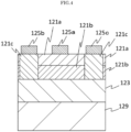
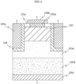
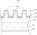
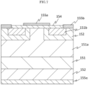
- FIG.3 to 9 show examples of using the oxide semiconductor film of the present inventive subject matter as a p-type semiconductor layer.
- an n-type semiconductor may be a semiconductor containing the same major component as major component of the oxide semiconductor film and an n-type dopant.
- the n-type semiconductor may be an n-type semiconductor containing a different major component that is different from the major component of the oxide semiconductor film.
- FIG.3 shows a schematic view of an embodiment of a Schottky barrier diode (SBD) according to the present inventive subject matter including an n - -type semiconductor layer 101a, an n + -type semiconductor layer 101b, a p-type semiconductor layer 102, a metal layer 103, an insulating layer 104, a Schottky electrode 105a and an Ohmic electrode 105b.
- the metal layer 103 is comprised of a metal such as aluminum and covers the Schottky electrode 105a.
- FIG.4 shows a schematic view of an embodiment of a high-electron-mobility transistor (HEMT) according to the present inventive subject matter including an n-type semiconductor layer with wide band gap 121a, an n-type semiconductor layer with narrow band gap 121b, an n + -type semiconductor layer 121c, a p-type semiconductor layer 123, a gate electrode 125a, a source electrode 125b, a drain electrode 125c, and a substrate 129.
- HEMT high-electron-mobility transistor
- FIG.5 shows a schematic view of an embodiment of a metal oxide semiconductor field-effect transistors (MOSFET) according to the present inventive subject matter.
- the MOSFET includes an n - -type semiconductor layer 131a, a first n + -type semiconductor layer 131b, a second n + -type semiconductor layer 131c, a p-type semiconductor layer 132, a p + -type semiconductor layer 132a, a gate insulating layer 134, a gate electrode 135a, a source electrode 135b and a drain electrode 135c.
- FIG.6 shows a schematic view of an embodiment of a junction field-effect transistors (JFET) according to the present inventive subject matter including an n - -type semiconductor layer 141a, a first n + -type semiconductor layer 141b, a second n + -type semiconductor layer 141c, a p-type semiconductor layer 142, a gate electrode 145a, a source electrode 145b and a drain electrode 145c.
- JFET junction field-effect transistors
- FIG.7 shows a schematic view of an embodiment of an insulated gate bipolar transistor (IGBT) according to the present inventive subject matter including an n-type semiconductor layer 151, an n - -type semiconductor layer 151a, an n + -type semiconductor layer 151b, a p-type semiconductor layer 152, a gate insulating layer 154, a gate electrode 155a, an emitter electrode 155b and a collector electrode 155c.
- IGBT insulated gate bipolar transistor
- FIG.8 shows a schematic view of an embodiment of a light emitting diode (LED) according to the present inventive subject matter.
- the LED shown in FIG.8 includes an n-type semiconductor layer 161 on a second electrode 165b, and a light emitting layer 163 is positioned on the n-type semiconductor layer 161. Also, a p-type semiconductor layer 162 is positioned on the light emitting layer 163.
- a first electrode is positioned on the light-transmitting electrode 167.
- a light emitting material used for the light emitting layer may be a known material.
- the light emitting device shown in FIG.8 may be covered with a protective layer except for the electrode portion.
- the material of the light-transmitting electrode may include oxide conductive material containing indium or titanium.
- the material may be In 2 O 3 , ZnO, SnO 2 , Ga 2 O 3 , TiO 2 , a mixed crystal thereof.
- the material may contain a dopant. By providing those materials using known method such as sputtering, the light-transmitting electrode would be formed. Also, annealing may be carried out after forming the light-transmitting electrode, in order to make the electrode more transparent.
- the light-emitting layer 163 is configured to emit light by applying a current to the p-type semiconductor layer 162, the light emitting layer 163, and the n-type semiconductor layer 161, through the first electrode 165a as a positive electrode and a second electrode 165b as a negative electrode.
- Examples of the material of the first electrode 165a and the second electrode 165b may include Al, Mo, Co, Zr, Sn, Nb, Fe, Cr, Ta, Ti, Au, Pt, V, Mn, Ni, Cu, Hf, W, Ir, Zn, Pd, Nd, Ag and/or alloys thereof, metal oxide conductive films such as tin oxide, zinc oxide, indium oxide, indium tin oxide (ITO), and indium zinc oxide (IZO), organic conductive compounds such as polyaniline, polythiophene, and polypyrrole, and mixtures of these materials.
- a forming method of the first and the second electrode is not particularly limited.
- Examples of the forming method of the first and the second electrode include wet methods such as printing method, spray method, coating method, physical methods such as vacuum deposition method, sputtering method, ion plating method, chemical methods such as CVD method, plasma CVD method.
- the forming method may be selected from above mentioned methods in consideration of a suitability for the material of the first electrode and the second electrode.
- FIG.9 shows a schematic view of another embodiment of a light emitting diode (LED) according to the present inventive subject matter.
- an n-type semiconductor layer 161 is arranged on the substrate 169, and the second electrode 165b is arranged on a part of the exposed surface of the n-type semiconductor layer 161, in which the exposed surface is formed by cutting out a part of a p-type semiconductor layer 162, light-emitting layer 163 and the n-type semiconductor layer 161.
- the semiconductor device may be used in a semiconductor system including a power source.
- the power source may be obtained by electrically connecting the semiconductor device to a wiring pattern using a known method.
- FIG. 10 shows a schematic view of a power system according to an embodiment of the present inventive subject matter.
- the semiconductor system of FIG.10 includes two or more power devices (power sources) and a control circuit.
- the power system may be used for a system device in combination with an electric circuit, as shown in FIG.11 .
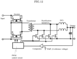
- FIG.12 shows a schematic view of a circuit diagram of a power supply circuit of a power device including a power circuit and a control circuit.
- a DC voltage is switched at high frequencies by an inverter 192 (configured with MOSFET A to D) to be converted to AC, followed by an insulation and transformation by a transformer 193.
- the voltage is the rectified by rectification MOSFETs 194 and the smoothed by a DCL 195 (smoothing coils L1 and L2) and a capacitor to output a direct current voltage.
- the output voltage is compared with a reference voltage by a voltage comparator to control the inverter and the rectification MOSFETs by a PWM control circuit to have a desired output voltage.
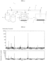
- the mist CVD apparatus 1 includes a carrier gas source 2a, a first flow-control valve 3a that is configured to control a flow of carrier gas sent from the carrier gas source 2a, a diluted carrier gas source 2b, a second flow-control valve 3a that is configured to control a flow of diluted carrier gas sent from the diluted carrier gas source 2b, a generator 4 of atomized droplets containing a raw material solution 4a, a vessel 5 containing water 5a, an ultrasonic transducer 6 attached to a bottom of the vessel 5, a film-formation chamber 7, a supply pipe 9 connecting from the generator 4 of atomized droplets to the film-formation chamber 7, a hot plate 8 arranged in the film-formation chamber 7, and an exhaust duct 11 that is configured to exhaust atomized droplets, droplets and gas after thermal reaction.
- a substrate 10 may be placed on
- Aluminum acetylacetonate (1.6g), rhodium acetylacetonate (0.06g), magnesium acetylacetonate (0.5g) and hydrochloric acid (6mL) were mixed with water (520mL) to make a raw-material solution.
- the raw-material solution 4a obtained at 2.
- Preparation of a Raw-Material Solution was contained in the generator 4 of atomized droplets. Then, a c-plane sapphire substrate was placed on the hot plate 8 as a substrate 10, and the hot plate 8 was activated to raise the temperature in the film-formation chamber 7 up to 550°C.
- the first flow-control valve 3a and the second flow-control valve 3b were opened to supply a carrier gas from the carrier gas source 2a and the diluted carrier gas source 2b, which are the source of carrier gas, into the film-formation chamber 7 to replace the atmosphere in the film-formation chamber 7 with the carrier gas.
- the flow rate of the carrier gas from the carrier gas source 2a was regulated at 2.0 L/min, and the diluted carrier gas from the diluted carrier gas source 2b was regulated at 0.5 L/min. In this embodiment, oxygen was used as the carrier gas.
- the ultrasonic transducer 6 was then vibrated at 2.4 MHz, and the vibration propagated through the water 5a to the raw material solution 4a to atomize the raw material solution 4a to form atomized droplets 4b.
- the atomized droplets 4b were sent through a supply pipe 9 with the carrier gas and introduced in the film-formation chamber 7.
- the atomized droplets were thermally reacted at 550°C under atmospheric pressure in the film-formation chamber 7 to form a film on the substrate 10.
- the film formation time was 12 hours.
- FIG.2 shows a result of XRD
- FIG. 13 shows result of SIMS.
- a Hall effect of the AlRhO film was measured and revealed to have the carrier type that was p-type, and carrier concentration that was 7.79 ⁇ 10 18 (/cm 3 ), and hole mobility that was 3 (cm 2 /Vs).
- An oxide semiconductor film according to the present inventive subject matter is useful as a p-type semiconductor, and applicable to semiconductor devices (e.g, compound semiconductor devices) and electronic components and electronic devices, optical and electronic photography related devices, and industrial parts. Since the oxide semiconductor film according to the present inventive subject matter has an enhanced p-type semiconductor property, the oxide semiconductor film is, in particular, applicable to semiconductor devices.
Landscapes
- Chemical & Material Sciences (AREA)
- Organic Chemistry (AREA)
- Inorganic Chemistry (AREA)
- Metallurgy (AREA)
- Materials Engineering (AREA)
- Mechanical Engineering (AREA)
- Engineering & Computer Science (AREA)
- Chemical Kinetics & Catalysis (AREA)
- General Chemical & Material Sciences (AREA)
- Liquid Deposition Of Substances Of Which Semiconductor Devices Are Composed (AREA)
- Thin Film Transistor (AREA)
- Chemical Vapour Deposition (AREA)
- Inorganic Compounds Of Heavy Metals (AREA)
- Junction Field-Effect Transistors (AREA)
Claims (11)
- Oxidhalbleiterfolie, umfassend:einen Dotierstoff vom p-Typ in der Oxidhalbleiterfolie, wobei der Dotierstoff vom p-Typ ein oder mehrere Elemente enthält, die ausgewählt sind aus Mg, H, Li, Na, K, Rb, Cs, Fr, Be, Ca, Sr, Ba, Ra, Mn, Fe, Ni, Pd, Cu, Ag, Au, Zn, Cd, Hg, Pb, N und P;eine p-Typ-Trägerkonzentration der Oxidhalbleiterfolie von 1×10¹⁵/cm3 oder mehr; undeine Lochmobilität der Oxidhalbleiterfolie von 1 cm2/Vs oder mehr;wobei die Oxidhalbleiterfolie ein Mischkristall eines Oxids eines Metalls der Gruppe 9 des Periodensystems und eines Oxids eines Metalls der Gruppe 13 des Periodensystems ist, undwobei die Oxidhalbleiterfolie eine elektrische Leitfähigkeit vom p-Typ aufweist.
- Oxidhalbleiterfolie nach Anspruch 1,
wobei das Metall der Gruppe 9 Rhodium, Iridium oder Kobalt umfasst. - Oxidhalbleiterfolie nach Anspruch 1 oder Anspruch 2,
wobei das Metall der Gruppe 13 mindestens ein Metall umfasst, das ausgewählt ist aus Indium, Aluminium und Gallium. - Oxidhalbleiterfolie nach einem der Ansprüche 1 bis 3,
wobei der Dotierstoff vom p-Typ Magnesium umfasst. - Halbleitervorrichtung, umfassend:eine Halbleiterschicht vom n-Typ, die ein Metalloxid umfasst, wobei das Metalloxid ein Metall der Gruppe 13 des Periodensystems beinhaltet;eine auf der Halbleiterschicht vom n-Typ ausgebildete Halbleiterschicht vom p-Typ, wobei die Halbleiterschicht vom p-Typ eine Oxidhalbleiterfolie nach einem der Ansprüche 1 bis 4 ist; undeine Elektrode.
- Halbleitervorrichtung nach Anspruch 5, ferner umfassend:
ein thermoelektrisches Umwandlungselement, das eine Halbleiterschicht vom p-Typ umfasst, die die Oxidhalbleiterfolie nach einem der Ansprüche 1 bis 4 umfasst. - Halbleitersystem, umfassend:
die Halbleitervorrichtung nach Anspruch 5 oder 6. - Verfahren zum Herstellen einer Oxidhalbleiterfolie nach einem der Ansprüche 1 bis 4, umfassend:Erzeugen von zerstäubten Tröpfchen durch Zerstäuben einer Rohmateriallösung, die ein Metall der Gruppe 9 des Periodensystems und ein Metall der Gruppe 13 des Periodensystems und einen Dotierstoff vom p-Typ beinhaltet, wobei der Dotierstoff vom p-Typ ein oder mehrere Elemente enthält, die ausgewählt sind aus Mg, H, Li, Na, K, Rb, Cs, Fr, Be, Ca, Sr, Ba, Ra, Mn, Fe, Ni, Pd, Cu, Ag, Au, Zn, Cd, Hg, Pb, N und P;Transportieren der zerstäubten Tröpfchen auf eine Fläche einer Basis unter Verwendung eines Trägergases; undAuslösen einer thermischen Reaktion der zerstäubten Tröpfchen angrenzend an die Fläche der Basis unter einer Sauerstoffatmosphäre, um die Oxidhalbleiterfolie auf der Basis zu bilden.
- Verfahren nach Anspruch 8,
wobei das Metall der Gruppe 9 Rhodium, Iridium oder Kobalt umfasst. - Verfahren nach Anspruch 8 oder Anspruch 9,
wobei das Metall der Gruppe 13 mindestens ein Metall umfasst, das ausgewählt ist aus Indium, Aluminium und Gallium. - Verfahren nach einem der Ansprüche 8 bis 10,
wobei der Dotierstoff vom p-Typ Magnesium umfasst.
Applications Claiming Priority (2)
| Application Number | Priority Date | Filing Date | Title |
|---|---|---|---|
| JP2016131158 | 2016-06-30 | ||
| PCT/JP2017/024274 WO2018004008A1 (ja) | 2016-06-30 | 2017-06-30 | 酸化物半導体膜及びその製造方法 |
Publications (3)
| Publication Number | Publication Date |
|---|---|
| EP3480840A1 EP3480840A1 (de) | 2019-05-08 |
| EP3480840A4 EP3480840A4 (de) | 2020-03-11 |
| EP3480840B1 true EP3480840B1 (de) | 2025-05-14 |
Family
ID=60786013
Family Applications (1)
| Application Number | Title | Priority Date | Filing Date |
|---|---|---|---|
| EP17820362.6A Active EP3480840B1 (de) | 2016-06-30 | 2017-06-30 | Oxidhalbleiterfolie und verfahren zur herstellung davon |
Country Status (6)
| Country | Link |
|---|---|
| US (1) | US11107926B2 (de) |
| EP (1) | EP3480840B1 (de) |
| JP (1) | JP6994183B2 (de) |
| KR (2) | KR102467802B1 (de) |
| CN (1) | CN109417037B (de) |
| WO (1) | WO2018004008A1 (de) |
Families Citing this family (16)
| Publication number | Priority date | Publication date | Assignee | Title |
|---|---|---|---|---|
| CN112424947A (zh) * | 2018-07-12 | 2021-02-26 | 株式会社Flosfia | 半导体装置及包含半导体装置的半导体系统 |
| WO2020013242A1 (ja) * | 2018-07-12 | 2020-01-16 | 株式会社Flosfia | 半導体装置 |
| EP3823041A4 (de) * | 2018-07-12 | 2022-04-20 | Flosfia Inc. | Halbleiterbauelement |
| TWI897850B (zh) * | 2018-07-12 | 2025-09-21 | 日商Flosfia股份有限公司 | 半導體裝置和半導體系統 |
| TWI879736B (zh) * | 2018-07-12 | 2025-04-11 | 日商Flosfia股份有限公司 | 半導體裝置和半導體系統 |
| WO2020013243A1 (ja) * | 2018-07-12 | 2020-01-16 | 株式会社Flosfia | 半導体装置 |
| TW202006945A (zh) | 2018-07-12 | 2020-02-01 | 日商Flosfia股份有限公司 | 半導體裝置和半導體系統 |
| WO2020183645A1 (ja) | 2019-03-13 | 2020-09-17 | 三菱電機株式会社 | 半導体装置 |
| CN110055591B (zh) * | 2019-05-17 | 2020-11-20 | 中国科学院物理研究所 | 二维三元原子晶体的制备方法 |
| CN114342086A (zh) | 2019-07-12 | 2022-04-12 | 株式会社Flosfia | 氧化物半导体膜及半导体装置 |
| JP7478334B2 (ja) * | 2020-01-10 | 2024-05-07 | 株式会社Flosfia | 半導体素子および半導体装置 |
| KR20220134639A (ko) * | 2020-02-07 | 2022-10-05 | 가부시키가이샤 플로스피아 | 반도체 소자 및 반도체 장치 |
| JP7247945B2 (ja) * | 2020-04-24 | 2023-03-29 | トヨタ自動車株式会社 | 酸化ガリウム系半導体及びその製造方法 |
| JP7531155B2 (ja) * | 2020-12-25 | 2024-08-09 | 株式会社デンソー | 酸化膜を有する製品の製造方法 |
| CN114518389B (zh) * | 2022-04-21 | 2022-07-12 | 北京中科海芯科技有限公司 | 一种气体传感器、制作方法及气体检测方法 |
| CN118507514B (zh) * | 2024-05-20 | 2024-11-01 | 深圳市港祥辉电子有限公司 | 一种纵向β氧化镓NPN晶体管的制备方法 |
Family Cites Families (22)
| Publication number | Priority date | Publication date | Assignee | Title |
|---|---|---|---|---|
| JPS5338039B2 (de) * | 1973-12-17 | 1978-10-13 | ||
| JP3701125B2 (ja) * | 1998-08-11 | 2005-09-28 | 日本特殊陶業株式会社 | ガスセンサ |
| TW454331B (en) * | 1999-06-16 | 2001-09-11 | Matsushita Electronics Corp | Semiconductor apparatus and its manufacturing method |
| TWI221341B (en) | 2003-09-18 | 2004-09-21 | Ind Tech Res Inst | Method and material for forming active layer of thin film transistor |
| WO2005047560A1 (ja) | 2003-11-17 | 2005-05-26 | Matsushita Electric Industrial Co., Ltd. | 結晶膜の製造方法、結晶膜付き基体の製造方法、熱電変換素子の製造方法、および熱電変換素子 |
| CN101673808B (zh) * | 2003-12-26 | 2012-05-23 | 株式会社半导体能源研究所 | 发光元件 |
| JP4831940B2 (ja) | 2004-05-24 | 2011-12-07 | 株式会社光波 | 半導体素子の製造方法 |
| JP4803634B2 (ja) * | 2004-10-01 | 2011-10-26 | 学校法人早稲田大学 | p型Ga2O3膜の製造方法およびpn接合型Ga2O3膜の製造方法 |
| US8013331B2 (en) * | 2006-06-19 | 2011-09-06 | Panasonic Corporation | Thin film transistor, method of manufacturing the same, and electronic device using the same |
| CN201754405U (zh) * | 2010-07-16 | 2011-03-02 | 北京工业大学 | 一种氧化锌掺杂同质pn结 |
| JP5352599B2 (ja) * | 2011-01-17 | 2013-11-27 | 株式会社半導体エネルギー研究所 | 半導体装置 |
| JP2012186231A (ja) * | 2011-03-03 | 2012-09-27 | Jsr Corp | 太陽電池 |
| JP5948581B2 (ja) | 2011-09-08 | 2016-07-06 | 株式会社Flosfia | Ga2O3系半導体素子 |
| JP5890991B2 (ja) * | 2011-09-28 | 2016-03-22 | トランスフォーム・ジャパン株式会社 | 化合物半導体装置及びその製造方法 |
| TWI581431B (zh) * | 2012-01-26 | 2017-05-01 | 半導體能源研究所股份有限公司 | 半導體裝置及半導體裝置的製造方法 |
| CN104620389B (zh) * | 2012-09-12 | 2017-11-17 | 夏普株式会社 | 半导体装置及其制造方法 |
| TWI495615B (zh) * | 2012-09-28 | 2015-08-11 | 財團法人工業技術研究院 | p型金屬氧化物半導體材料 |
| US20150087110A1 (en) * | 2013-09-21 | 2015-03-26 | Northwestern University | Low-Temperature Fabrication of Spray-Coated Metal Oxide Thin Film Transistors |
| JP6547273B2 (ja) * | 2013-12-26 | 2019-07-24 | 株式会社リコー | p型酸化物半導体、p型酸化物半導体製造用組成物、p型酸化物半導体の製造方法、半導体素子、表示素子、画像表示装置、及びシステム |
| JP6945120B2 (ja) | 2014-08-29 | 2021-10-06 | 株式会社Flosfia | 金属膜形成方法 |
| JP2016081946A (ja) | 2014-10-09 | 2016-05-16 | 株式会社Flosfia | 半導体構造および半導体装置 |
| US9647135B2 (en) * | 2015-01-22 | 2017-05-09 | Snaptrack, Inc. | Tin based p-type oxide semiconductor and thin film transistor applications |
-
2017
- 2017-06-30 KR KR1020227006715A patent/KR102467802B1/ko active Active
- 2017-06-30 CN CN201780040595.5A patent/CN109417037B/zh active Active
- 2017-06-30 US US16/313,239 patent/US11107926B2/en active Active
- 2017-06-30 KR KR1020187037577A patent/KR20190022561A/ko not_active Ceased
- 2017-06-30 WO PCT/JP2017/024274 patent/WO2018004008A1/ja not_active Ceased
- 2017-06-30 EP EP17820362.6A patent/EP3480840B1/de active Active
- 2017-06-30 JP JP2018525322A patent/JP6994183B2/ja active Active
Also Published As
| Publication number | Publication date |
|---|---|
| CN109417037B (zh) | 2024-03-15 |
| JP6994183B2 (ja) | 2022-01-14 |
| CN109417037A (zh) | 2019-03-01 |
| JPWO2018004008A1 (ja) | 2019-05-30 |
| KR20220031143A (ko) | 2022-03-11 |
| US11107926B2 (en) | 2021-08-31 |
| WO2018004008A1 (ja) | 2018-01-04 |
| KR102467802B1 (ko) | 2022-11-16 |
| US20190157400A1 (en) | 2019-05-23 |
| EP3480840A4 (de) | 2020-03-11 |
| KR20190022561A (ko) | 2019-03-06 |
| EP3480840A1 (de) | 2019-05-08 |
Similar Documents
| Publication | Publication Date | Title |
|---|---|---|
| EP3509090B1 (de) | Halbleiterbauelement mit p-typ oxidhalbleiter und halbleitersystem damit | |
| EP3480840A1 (de) | Oxidhalbleiterfolie und verfahren zur herstellung davon | |
| US11916103B2 (en) | P-type oxide semiconductor and method for manufacturing same | |
| JP7274701B2 (ja) | p型酸化物半導体膜及びその形成方法 | |
| JP6994181B2 (ja) | 結晶性酸化物半導体膜および半導体装置 | |
| JP7358718B2 (ja) | 結晶性酸化物半導体膜および半導体装置 | |
| WO2022030648A2 (ja) | p型酸化物半導体及びp型酸化物半導体を含む半導体装置 | |
| JP2022030646A (ja) | 酸化物半導体及び酸化物半導体を含む半導体装置 | |
| JP7678955B2 (ja) | p型酸化物半導体及びp型酸化物半導体を含む半導体装置 | |
| WO2019098294A1 (ja) | p型酸化物半導体膜の形成方法 |
Legal Events
| Date | Code | Title | Description |
|---|---|---|---|
| STAA | Information on the status of an ep patent application or granted ep patent |
Free format text: STATUS: THE INTERNATIONAL PUBLICATION HAS BEEN MADE |
|
| PUAI | Public reference made under article 153(3) epc to a published international application that has entered the european phase |
Free format text: ORIGINAL CODE: 0009012 |
|
| STAA | Information on the status of an ep patent application or granted ep patent |
Free format text: STATUS: REQUEST FOR EXAMINATION WAS MADE |
|
| 17P | Request for examination filed |
Effective date: 20190102 |
|
| AK | Designated contracting states |
Kind code of ref document: A1 Designated state(s): AL AT BE BG CH CY CZ DE DK EE ES FI FR GB GR HR HU IE IS IT LI LT LU LV MC MK MT NL NO PL PT RO RS SE SI SK SM TR |
|
| AX | Request for extension of the european patent |
Extension state: BA ME |
|
| RAP1 | Party data changed (applicant data changed or rights of an application transferred) |
Owner name: FLOSFIA INC. |
|
| DAV | Request for validation of the european patent (deleted) | ||
| DAX | Request for extension of the european patent (deleted) | ||
| A4 | Supplementary search report drawn up and despatched |
Effective date: 20200206 |
|
| RIC1 | Information provided on ipc code assigned before grant |
Ipc: H01L 21/36 20060101AFI20200131BHEP Ipc: C23C 18/12 20060101ALI20200131BHEP Ipc: H01L 33/02 20100101ALI20200131BHEP Ipc: H01L 29/778 20060101ALI20200131BHEP Ipc: H01L 21/338 20060101ALI20200131BHEP Ipc: H01L 21/337 20060101ALI20200131BHEP Ipc: H01L 29/06 20060101ALI20200131BHEP Ipc: H01L 29/24 20060101ALI20200131BHEP Ipc: H01L 21/368 20060101ALI20200131BHEP Ipc: C01G 55/00 20060101ALI20200131BHEP Ipc: H01L 29/812 20060101ALI20200131BHEP Ipc: H01L 29/739 20060101ALI20200131BHEP Ipc: H01L 29/78 20060101ALI20200131BHEP Ipc: H01L 29/786 20060101ALI20200131BHEP Ipc: H01L 29/808 20060101ALI20200131BHEP Ipc: H01L 21/336 20060101ALI20200131BHEP Ipc: H01L 29/12 20060101ALI20200131BHEP Ipc: H01L 29/872 20060101ALI20200131BHEP |
|
| STAA | Information on the status of an ep patent application or granted ep patent |
Free format text: STATUS: EXAMINATION IS IN PROGRESS |
|
| 17Q | First examination report despatched |
Effective date: 20210826 |
|
| REG | Reference to a national code |
Ref country code: DE Ref legal event code: R079 Free format text: PREVIOUS MAIN CLASS: H01L0021365000 Ref document number: 602017089474 Country of ref document: DE Ipc: H01L0021368000 |
|
| GRAP | Despatch of communication of intention to grant a patent |
Free format text: ORIGINAL CODE: EPIDOSNIGR1 |
|
| STAA | Information on the status of an ep patent application or granted ep patent |
Free format text: STATUS: GRANT OF PATENT IS INTENDED |
|
| RIC1 | Information provided on ipc code assigned before grant |
Ipc: C23C 16/448 20060101ALI20250121BHEP Ipc: C23C 16/40 20060101ALI20250121BHEP Ipc: H10D 12/00 20250101ALI20250121BHEP Ipc: H10D 8/60 20250101ALI20250121BHEP Ipc: H10N 10/855 20230101ALI20250121BHEP Ipc: H10D 62/80 20250101ALI20250121BHEP Ipc: H10D 30/87 20250101ALI20250121BHEP Ipc: H10D 30/67 20250101ALI20250121BHEP Ipc: H10H 20/81 20250101ALI20250121BHEP Ipc: C23C 18/12 20060101ALI20250121BHEP Ipc: C01G 55/00 20060101ALI20250121BHEP Ipc: H01L 21/368 20060101AFI20250121BHEP |
|
| INTG | Intention to grant announced |
Effective date: 20250210 |
|
| RIN1 | Information on inventor provided before grant (corrected) |
Inventor name: HITORA, TOSHIMI Inventor name: TANIKAWA, TOMOCHIKA |
|
| GRAS | Grant fee paid |
Free format text: ORIGINAL CODE: EPIDOSNIGR3 |
|
| GRAA | (expected) grant |
Free format text: ORIGINAL CODE: 0009210 |
|
| STAA | Information on the status of an ep patent application or granted ep patent |
Free format text: STATUS: THE PATENT HAS BEEN GRANTED |
|
| AK | Designated contracting states |
Kind code of ref document: B1 Designated state(s): AL AT BE BG CH CY CZ DE DK EE ES FI FR GB GR HR HU IE IS IT LI LT LU LV MC MK MT NL NO PL PT RO RS SE SI SK SM TR |
|
| REG | Reference to a national code |
Ref country code: GB Ref legal event code: FG4D |
|
| REG | Reference to a national code |
Ref country code: CH Ref legal event code: EP |
|
| REG | Reference to a national code |
Ref country code: DE Ref legal event code: R096 Ref document number: 602017089474 Country of ref document: DE |
|
| REG | Reference to a national code |
Ref country code: IE Ref legal event code: FG4D |
|
| P01 | Opt-out of the competence of the unified patent court (upc) registered |
Free format text: CASE NUMBER: APP_25984/2025 Effective date: 20250602 |
|
| REG | Reference to a national code |
Ref country code: NL Ref legal event code: MP Effective date: 20250514 |
|
| PG25 | Lapsed in a contracting state [announced via postgrant information from national office to epo] |
Ref country code: PT Free format text: LAPSE BECAUSE OF FAILURE TO SUBMIT A TRANSLATION OF THE DESCRIPTION OR TO PAY THE FEE WITHIN THE PRESCRIBED TIME-LIMIT Effective date: 20250915 Ref country code: FI Free format text: LAPSE BECAUSE OF FAILURE TO SUBMIT A TRANSLATION OF THE DESCRIPTION OR TO PAY THE FEE WITHIN THE PRESCRIBED TIME-LIMIT Effective date: 20250514 Ref country code: ES Free format text: LAPSE BECAUSE OF FAILURE TO SUBMIT A TRANSLATION OF THE DESCRIPTION OR TO PAY THE FEE WITHIN THE PRESCRIBED TIME-LIMIT Effective date: 20250514 |
|
| REG | Reference to a national code |
Ref country code: LT Ref legal event code: MG9D |
|
| PG25 | Lapsed in a contracting state [announced via postgrant information from national office to epo] |
Ref country code: NO Free format text: LAPSE BECAUSE OF FAILURE TO SUBMIT A TRANSLATION OF THE DESCRIPTION OR TO PAY THE FEE WITHIN THE PRESCRIBED TIME-LIMIT Effective date: 20250814 Ref country code: GR Free format text: LAPSE BECAUSE OF FAILURE TO SUBMIT A TRANSLATION OF THE DESCRIPTION OR TO PAY THE FEE WITHIN THE PRESCRIBED TIME-LIMIT Effective date: 20250815 |
|
| PG25 | Lapsed in a contracting state [announced via postgrant information from national office to epo] |
Ref country code: NL Free format text: LAPSE BECAUSE OF FAILURE TO SUBMIT A TRANSLATION OF THE DESCRIPTION OR TO PAY THE FEE WITHIN THE PRESCRIBED TIME-LIMIT Effective date: 20250514 Ref country code: PL Free format text: LAPSE BECAUSE OF FAILURE TO SUBMIT A TRANSLATION OF THE DESCRIPTION OR TO PAY THE FEE WITHIN THE PRESCRIBED TIME-LIMIT Effective date: 20250514 |
|
| REG | Reference to a national code |
Ref country code: AT Ref legal event code: MK05 Ref document number: 1795567 Country of ref document: AT Kind code of ref document: T Effective date: 20250514 |
|
| PG25 | Lapsed in a contracting state [announced via postgrant information from national office to epo] |
Ref country code: BG Free format text: LAPSE BECAUSE OF FAILURE TO SUBMIT A TRANSLATION OF THE DESCRIPTION OR TO PAY THE FEE WITHIN THE PRESCRIBED TIME-LIMIT Effective date: 20250514 |
|
| PGFP | Annual fee paid to national office [announced via postgrant information from national office to epo] |
Ref country code: GB Payment date: 20250926 Year of fee payment: 9 |
|
| PG25 | Lapsed in a contracting state [announced via postgrant information from national office to epo] |
Ref country code: HR Free format text: LAPSE BECAUSE OF FAILURE TO SUBMIT A TRANSLATION OF THE DESCRIPTION OR TO PAY THE FEE WITHIN THE PRESCRIBED TIME-LIMIT Effective date: 20250514 |
|
| PG25 | Lapsed in a contracting state [announced via postgrant information from national office to epo] |
Ref country code: AT Free format text: LAPSE BECAUSE OF FAILURE TO SUBMIT A TRANSLATION OF THE DESCRIPTION OR TO PAY THE FEE WITHIN THE PRESCRIBED TIME-LIMIT Effective date: 20250514 |
|
| PG25 | Lapsed in a contracting state [announced via postgrant information from national office to epo] |
Ref country code: RS Free format text: LAPSE BECAUSE OF FAILURE TO SUBMIT A TRANSLATION OF THE DESCRIPTION OR TO PAY THE FEE WITHIN THE PRESCRIBED TIME-LIMIT Effective date: 20250814 |
|
| PG25 | Lapsed in a contracting state [announced via postgrant information from national office to epo] |
Ref country code: IS Free format text: LAPSE BECAUSE OF FAILURE TO SUBMIT A TRANSLATION OF THE DESCRIPTION OR TO PAY THE FEE WITHIN THE PRESCRIBED TIME-LIMIT Effective date: 20250914 |
|
| PG25 | Lapsed in a contracting state [announced via postgrant information from national office to epo] |
Ref country code: LV Free format text: LAPSE BECAUSE OF FAILURE TO SUBMIT A TRANSLATION OF THE DESCRIPTION OR TO PAY THE FEE WITHIN THE PRESCRIBED TIME-LIMIT Effective date: 20250514 |
|
| REG | Reference to a national code |
Ref country code: DE Ref legal event code: R079 Ref document number: 602017089474 Country of ref document: DE Free format text: PREVIOUS MAIN CLASS: H01L0021368000 Ipc: H10P0014260000 |
|
| PGFP | Annual fee paid to national office [announced via postgrant information from national office to epo] |
Ref country code: DE Payment date: 20250930 Year of fee payment: 9 |
|
| PG25 | Lapsed in a contracting state [announced via postgrant information from national office to epo] |
Ref country code: SM Free format text: LAPSE BECAUSE OF FAILURE TO SUBMIT A TRANSLATION OF THE DESCRIPTION OR TO PAY THE FEE WITHIN THE PRESCRIBED TIME-LIMIT Effective date: 20250514 Ref country code: DK Free format text: LAPSE BECAUSE OF FAILURE TO SUBMIT A TRANSLATION OF THE DESCRIPTION OR TO PAY THE FEE WITHIN THE PRESCRIBED TIME-LIMIT Effective date: 20250514 |
|
| PGFP | Annual fee paid to national office [announced via postgrant information from national office to epo] |
Ref country code: FR Payment date: 20251013 Year of fee payment: 9 |
|
| PG25 | Lapsed in a contracting state [announced via postgrant information from national office to epo] |
Ref country code: CZ Free format text: LAPSE BECAUSE OF FAILURE TO SUBMIT A TRANSLATION OF THE DESCRIPTION OR TO PAY THE FEE WITHIN THE PRESCRIBED TIME-LIMIT Effective date: 20250514 |
|
| PG25 | Lapsed in a contracting state [announced via postgrant information from national office to epo] |
Ref country code: EE Free format text: LAPSE BECAUSE OF FAILURE TO SUBMIT A TRANSLATION OF THE DESCRIPTION OR TO PAY THE FEE WITHIN THE PRESCRIBED TIME-LIMIT Effective date: 20250514 |
|
| PG25 | Lapsed in a contracting state [announced via postgrant information from national office to epo] |
Ref country code: SK Free format text: LAPSE BECAUSE OF FAILURE TO SUBMIT A TRANSLATION OF THE DESCRIPTION OR TO PAY THE FEE WITHIN THE PRESCRIBED TIME-LIMIT Effective date: 20250514 Ref country code: RO Free format text: LAPSE BECAUSE OF FAILURE TO SUBMIT A TRANSLATION OF THE DESCRIPTION OR TO PAY THE FEE WITHIN THE PRESCRIBED TIME-LIMIT Effective date: 20250514 |
|
| REG | Reference to a national code |
Ref country code: CH Ref legal event code: H13 Free format text: ST27 STATUS EVENT CODE: U-0-0-H10-H13 (AS PROVIDED BY THE NATIONAL OFFICE) Effective date: 20260127 |
|
| PG25 | Lapsed in a contracting state [announced via postgrant information from national office to epo] |
Ref country code: IT Free format text: LAPSE BECAUSE OF FAILURE TO SUBMIT A TRANSLATION OF THE DESCRIPTION OR TO PAY THE FEE WITHIN THE PRESCRIBED TIME-LIMIT Effective date: 20250514 |
|
| PG25 | Lapsed in a contracting state [announced via postgrant information from national office to epo] |
Ref country code: LU Free format text: LAPSE BECAUSE OF NON-PAYMENT OF DUE FEES Effective date: 20250630 |
|
| REG | Reference to a national code |
Ref country code: DE Ref legal event code: R097 Ref document number: 602017089474 Country of ref document: DE |
|
| PG25 | Lapsed in a contracting state [announced via postgrant information from national office to epo] |
Ref country code: MC Free format text: LAPSE BECAUSE OF FAILURE TO SUBMIT A TRANSLATION OF THE DESCRIPTION OR TO PAY THE FEE WITHIN THE PRESCRIBED TIME-LIMIT Effective date: 20250514 |
|
| REG | Reference to a national code |
Ref country code: BE Ref legal event code: MM Effective date: 20250630 |
|
| PLBE | No opposition filed within time limit |
Free format text: ORIGINAL CODE: 0009261 |
|
| STAA | Information on the status of an ep patent application or granted ep patent |
Free format text: STATUS: NO OPPOSITION FILED WITHIN TIME LIMIT |
|
| REG | Reference to a national code |
Ref country code: CH Ref legal event code: L10 Free format text: ST27 STATUS EVENT CODE: U-0-0-L10-L00 (AS PROVIDED BY THE NATIONAL OFFICE) Effective date: 20260325 |
|
| PG25 | Lapsed in a contracting state [announced via postgrant information from national office to epo] |
Ref country code: IE Free format text: LAPSE BECAUSE OF NON-PAYMENT OF DUE FEES Effective date: 20250630 |
|
| PG25 | Lapsed in a contracting state [announced via postgrant information from national office to epo] |
Ref country code: BE Free format text: LAPSE BECAUSE OF NON-PAYMENT OF DUE FEES Effective date: 20250630 |
|
| 26N | No opposition filed |
Effective date: 20260217 |
|
| PG25 | Lapsed in a contracting state [announced via postgrant information from national office to epo] |
Ref country code: CH Free format text: LAPSE BECAUSE OF NON-PAYMENT OF DUE FEES Effective date: 20250630 |