EP3473627B1 - Composé hétérocyclique et dispositif électronique organique le comprenant - Google Patents
Composé hétérocyclique et dispositif électronique organique le comprenant Download PDFInfo
- Publication number
- EP3473627B1 EP3473627B1 EP18805836.6A EP18805836A EP3473627B1 EP 3473627 B1 EP3473627 B1 EP 3473627B1 EP 18805836 A EP18805836 A EP 18805836A EP 3473627 B1 EP3473627 B1 EP 3473627B1
- Authority
- EP
- European Patent Office
- Prior art keywords
- group
- substituted
- same
- organic
- unsubstituted
- Prior art date
- Legal status (The legal status is an assumption and is not a legal conclusion. Google has not performed a legal analysis and makes no representation as to the accuracy of the status listed.)
- Active
Links
- 150000002391 heterocyclic compounds Chemical class 0.000 title claims description 41
- -1 GeRR' Inorganic materials 0.000 claims description 78
- 239000000126 substance Substances 0.000 claims description 72
- 125000003118 aryl group Chemical group 0.000 claims description 46
- 150000001875 compounds Chemical class 0.000 claims description 42
- 125000000217 alkyl group Chemical group 0.000 claims description 41
- 239000000463 material Substances 0.000 claims description 37
- 239000011368 organic material Substances 0.000 claims description 35
- 229910052739 hydrogen Inorganic materials 0.000 claims description 23
- 239000001257 hydrogen Substances 0.000 claims description 23
- UFHFLCQGNIYNRP-UHFFFAOYSA-N Hydrogen Chemical compound [H][H] UFHFLCQGNIYNRP-UHFFFAOYSA-N 0.000 claims description 22
- 125000003545 alkoxy group Chemical group 0.000 claims description 22
- 125000005843 halogen group Chemical group 0.000 claims description 18
- 125000001072 heteroaryl group Chemical group 0.000 claims description 18
- YZCKVEUIGOORGS-OUBTZVSYSA-N Deuterium Chemical compound [2H] YZCKVEUIGOORGS-OUBTZVSYSA-N 0.000 claims description 11
- 229910052805 deuterium Inorganic materials 0.000 claims description 11
- 125000002887 hydroxy group Chemical group [H]O* 0.000 claims description 11
- 125000005309 thioalkoxy group Chemical group 0.000 claims description 10
- 125000005842 heteroatom Chemical group 0.000 claims description 9
- 229910052717 sulfur Inorganic materials 0.000 claims description 9
- 229910052711 selenium Inorganic materials 0.000 claims description 8
- 239000010409 thin film Substances 0.000 claims description 5
- 230000000052 comparative effect Effects 0.000 description 79
- 238000004519 manufacturing process Methods 0.000 description 34
- 239000000243 solution Substances 0.000 description 24
- YTPLMLYBLZKORZ-UHFFFAOYSA-N Thiophene Chemical group C=1C=CSC=1 YTPLMLYBLZKORZ-UHFFFAOYSA-N 0.000 description 23
- 229940125782 compound 2 Drugs 0.000 description 22
- 238000000034 method Methods 0.000 description 21
- VZSRBBMJRBPUNF-UHFFFAOYSA-N 2-(2,3-dihydro-1H-inden-2-ylamino)-N-[3-oxo-3-(2,4,6,7-tetrahydrotriazolo[4,5-c]pyridin-5-yl)propyl]pyrimidine-5-carboxamide Chemical compound C1C(CC2=CC=CC=C12)NC1=NC=C(C=N1)C(=O)NCCC(N1CC2=C(CC1)NN=N2)=O VZSRBBMJRBPUNF-UHFFFAOYSA-N 0.000 description 20
- 239000000758 substrate Substances 0.000 description 20
- 125000004432 carbon atom Chemical group C* 0.000 description 17
- 229940125904 compound 1 Drugs 0.000 description 16
- 125000001280 n-hexyl group Chemical group C(CCCCC)* 0.000 description 15
- MKYBYDHXWVHEJW-UHFFFAOYSA-N N-[1-oxo-1-(2,4,6,7-tetrahydrotriazolo[4,5-c]pyridin-5-yl)propan-2-yl]-2-[[3-(trifluoromethoxy)phenyl]methylamino]pyrimidine-5-carboxamide Chemical compound O=C(C(C)NC(=O)C=1C=NC(=NC=1)NCC1=CC(=CC=C1)OC(F)(F)F)N1CC2=C(CC1)NN=N2 MKYBYDHXWVHEJW-UHFFFAOYSA-N 0.000 description 14
- NIPNSKYNPDTRPC-UHFFFAOYSA-N N-[2-oxo-2-(2,4,6,7-tetrahydrotriazolo[4,5-c]pyridin-5-yl)ethyl]-2-[[3-(trifluoromethoxy)phenyl]methylamino]pyrimidine-5-carboxamide Chemical compound O=C(CNC(=O)C=1C=NC(=NC=1)NCC1=CC(=CC=C1)OC(F)(F)F)N1CC2=C(CC1)NN=N2 NIPNSKYNPDTRPC-UHFFFAOYSA-N 0.000 description 14
- AFCARXCZXQIEQB-UHFFFAOYSA-N N-[3-oxo-3-(2,4,6,7-tetrahydrotriazolo[4,5-c]pyridin-5-yl)propyl]-2-[[3-(trifluoromethoxy)phenyl]methylamino]pyrimidine-5-carboxamide Chemical compound O=C(CCNC(=O)C=1C=NC(=NC=1)NCC1=CC(=CC=C1)OC(F)(F)F)N1CC2=C(CC1)NN=N2 AFCARXCZXQIEQB-UHFFFAOYSA-N 0.000 description 14
- XLOMVQKBTHCTTD-UHFFFAOYSA-N Zinc monoxide Chemical compound [Zn]=O XLOMVQKBTHCTTD-UHFFFAOYSA-N 0.000 description 13
- 239000002131 composite material Substances 0.000 description 13
- 125000002950 monocyclic group Chemical group 0.000 description 12
- 125000001997 phenyl group Chemical group [H]C1=C([H])C([H])=C(*)C([H])=C1[H] 0.000 description 12
- 125000003367 polycyclic group Chemical group 0.000 description 12
- 238000002360 preparation method Methods 0.000 description 11
- 0 CC(CC(*)(C*)N)*(*)=C Chemical compound CC(CC(*)(C*)N)*(*)=C 0.000 description 10
- HEDRZPFGACZZDS-UHFFFAOYSA-N Chloroform Chemical compound ClC(Cl)Cl HEDRZPFGACZZDS-UHFFFAOYSA-N 0.000 description 10
- KFZMGEQAYNKOFK-UHFFFAOYSA-N Isopropanol Chemical compound CC(C)O KFZMGEQAYNKOFK-UHFFFAOYSA-N 0.000 description 9
- 238000010521 absorption reaction Methods 0.000 description 9
- 238000006243 chemical reaction Methods 0.000 description 9
- 125000001424 substituent group Chemical group 0.000 description 9
- HEDRZPFGACZZDS-MICDWDOJSA-N Trichloro(2H)methane Chemical compound [2H]C(Cl)(Cl)Cl HEDRZPFGACZZDS-MICDWDOJSA-N 0.000 description 8
- 229910052731 fluorine Inorganic materials 0.000 description 8
- 239000011737 fluorine Substances 0.000 description 8
- ZSWFCLXCOIISFI-UHFFFAOYSA-N cyclopentadiene Chemical group C1C=CC=C1 ZSWFCLXCOIISFI-UHFFFAOYSA-N 0.000 description 7
- 125000003983 fluorenyl group Chemical group C1(=CC=CC=2C3=CC=CC=C3CC12)* 0.000 description 7
- 230000001965 increasing effect Effects 0.000 description 7
- 125000003454 indenyl group Chemical group C1(C=CC2=CC=CC=C12)* 0.000 description 7
- 238000004768 lowest unoccupied molecular orbital Methods 0.000 description 7
- 239000000203 mixture Substances 0.000 description 7
- AICOOMRHRUFYCM-ZRRPKQBOSA-N oxazine, 1 Chemical compound C([C@@H]1[C@H](C(C[C@]2(C)[C@@H]([C@H](C)N(C)C)[C@H](O)C[C@]21C)=O)CC1=CC2)C[C@H]1[C@@]1(C)[C@H]2N=C(C(C)C)OC1 AICOOMRHRUFYCM-ZRRPKQBOSA-N 0.000 description 7
- YMWUJEATGCHHMB-UHFFFAOYSA-N Dichloromethane Chemical compound ClCCl YMWUJEATGCHHMB-UHFFFAOYSA-N 0.000 description 6
- 239000000654 additive Substances 0.000 description 6
- 125000001931 aliphatic group Chemical group 0.000 description 6
- 125000005264 aryl amine group Chemical group 0.000 description 6
- 239000010408 film Substances 0.000 description 6
- 239000011787 zinc oxide Substances 0.000 description 6
- 238000005160 1H NMR spectroscopy Methods 0.000 description 5
- PXGOKWXKJXAPGV-UHFFFAOYSA-N Fluorine Chemical compound FF PXGOKWXKJXAPGV-UHFFFAOYSA-N 0.000 description 5
- 229910052760 oxygen Inorganic materials 0.000 description 5
- 230000008569 process Effects 0.000 description 5
- 239000002904 solvent Substances 0.000 description 5
- HMUNWXXNJPVALC-UHFFFAOYSA-N 1-[4-[2-(2,3-dihydro-1H-inden-2-ylamino)pyrimidin-5-yl]piperazin-1-yl]-2-(2,4,6,7-tetrahydrotriazolo[4,5-c]pyridin-5-yl)ethanone Chemical compound C1C(CC2=CC=CC=C12)NC1=NC=C(C=N1)N1CCN(CC1)C(CN1CC2=C(CC1)NN=N2)=O HMUNWXXNJPVALC-UHFFFAOYSA-N 0.000 description 4
- LDXJRKWFNNFDSA-UHFFFAOYSA-N 2-(2,4,6,7-tetrahydrotriazolo[4,5-c]pyridin-5-yl)-1-[4-[2-[[3-(trifluoromethoxy)phenyl]methylamino]pyrimidin-5-yl]piperazin-1-yl]ethanone Chemical compound C1CN(CC2=NNN=C21)CC(=O)N3CCN(CC3)C4=CN=C(N=C4)NCC5=CC(=CC=C5)OC(F)(F)F LDXJRKWFNNFDSA-UHFFFAOYSA-N 0.000 description 4
- YLZOPXRUQYQQID-UHFFFAOYSA-N 3-(2,4,6,7-tetrahydrotriazolo[4,5-c]pyridin-5-yl)-1-[4-[2-[[3-(trifluoromethoxy)phenyl]methylamino]pyrimidin-5-yl]piperazin-1-yl]propan-1-one Chemical compound N1N=NC=2CN(CCC=21)CCC(=O)N1CCN(CC1)C=1C=NC(=NC=1)NCC1=CC(=CC=C1)OC(F)(F)F YLZOPXRUQYQQID-UHFFFAOYSA-N 0.000 description 4
- CSCPPACGZOOCGX-UHFFFAOYSA-N Acetone Chemical compound CC(C)=O CSCPPACGZOOCGX-UHFFFAOYSA-N 0.000 description 4
- CBENFWSGALASAD-UHFFFAOYSA-N Ozone Chemical compound [O-][O+]=O CBENFWSGALASAD-UHFFFAOYSA-N 0.000 description 4
- JUJWROOIHBZHMG-UHFFFAOYSA-N Pyridine Chemical compound C1=CC=NC=C1 JUJWROOIHBZHMG-UHFFFAOYSA-N 0.000 description 4
- 230000000996 additive effect Effects 0.000 description 4
- 150000001555 benzenes Chemical group 0.000 description 4
- MVPPADPHJFYWMZ-UHFFFAOYSA-N chlorobenzene Chemical compound ClC1=CC=CC=C1 MVPPADPHJFYWMZ-UHFFFAOYSA-N 0.000 description 4
- 125000000753 cycloalkyl group Chemical group 0.000 description 4
- USIUVYZYUHIAEV-UHFFFAOYSA-N diphenyl ether Chemical compound C=1C=CC=CC=1OC1=CC=CC=C1 USIUVYZYUHIAEV-UHFFFAOYSA-N 0.000 description 4
- 230000000694 effects Effects 0.000 description 4
- 125000000623 heterocyclic group Chemical group 0.000 description 4
- 238000002347 injection Methods 0.000 description 4
- 239000007924 injection Substances 0.000 description 4
- 230000003993 interaction Effects 0.000 description 4
- 229910052751 metal Inorganic materials 0.000 description 4
- 239000002184 metal Substances 0.000 description 4
- JKQOBWVOAYFWKG-UHFFFAOYSA-N molybdenum trioxide Chemical compound O=[Mo](=O)=O JKQOBWVOAYFWKG-UHFFFAOYSA-N 0.000 description 4
- XLYOFNOQVPJJNP-UHFFFAOYSA-N water Substances O XLYOFNOQVPJJNP-UHFFFAOYSA-N 0.000 description 4
- XEKOWRVHYACXOJ-UHFFFAOYSA-N Ethyl acetate Chemical compound CCOC(C)=O XEKOWRVHYACXOJ-UHFFFAOYSA-N 0.000 description 3
- ZMXDDKWLCZADIW-UHFFFAOYSA-N N,N-Dimethylformamide Chemical compound CN(C)C=O ZMXDDKWLCZADIW-UHFFFAOYSA-N 0.000 description 3
- LRHPLDYGYMQRHN-UHFFFAOYSA-N N-Butanol Chemical compound CCCCO LRHPLDYGYMQRHN-UHFFFAOYSA-N 0.000 description 3
- MUBZPKHOEPUJKR-UHFFFAOYSA-N Oxalic acid Chemical compound OC(=O)C(O)=O MUBZPKHOEPUJKR-UHFFFAOYSA-N 0.000 description 3
- HEMHJVSKTPXQMS-UHFFFAOYSA-M Sodium hydroxide Chemical compound [OH-].[Na+] HEMHJVSKTPXQMS-UHFFFAOYSA-M 0.000 description 3
- 125000005332 alkyl sulfoxy group Chemical group 0.000 description 3
- 125000005377 alkyl thioxy group Chemical group 0.000 description 3
- 229910052782 aluminium Inorganic materials 0.000 description 3
- 125000003368 amide group Chemical group 0.000 description 3
- 125000004104 aryloxy group Chemical group 0.000 description 3
- 125000004429 atom Chemical group 0.000 description 3
- 239000000470 constituent Substances 0.000 description 3
- 239000012153 distilled water Substances 0.000 description 3
- 238000000605 extraction Methods 0.000 description 3
- 125000001153 fluoro group Chemical group F* 0.000 description 3
- 239000011521 glass Substances 0.000 description 3
- 150000002430 hydrocarbons Chemical group 0.000 description 3
- 230000004048 modification Effects 0.000 description 3
- 238000012986 modification Methods 0.000 description 3
- 230000001590 oxidative effect Effects 0.000 description 3
- JTPNRXUCIXHOKM-UHFFFAOYSA-N 1-chloronaphthalene Chemical compound C1=CC=C2C(Cl)=CC=CC2=C1 JTPNRXUCIXHOKM-UHFFFAOYSA-N 0.000 description 2
- 125000005916 2-methylpentyl group Chemical group 0.000 description 2
- UJOBWOGCFQCDNV-UHFFFAOYSA-N 9H-carbazole Chemical compound C1=CC=C2C3=CC=CC=C3NC2=C1 UJOBWOGCFQCDNV-UHFFFAOYSA-N 0.000 description 2
- ZOXJGFHDIHLPTG-UHFFFAOYSA-N Boron Chemical group [B] ZOXJGFHDIHLPTG-UHFFFAOYSA-N 0.000 description 2
- XMWRBQBLMFGWIX-UHFFFAOYSA-N C60 fullerene Chemical compound C12=C3C(C4=C56)=C7C8=C5C5=C9C%10=C6C6=C4C1=C1C4=C6C6=C%10C%10=C9C9=C%11C5=C8C5=C8C7=C3C3=C7C2=C1C1=C2C4=C6C4=C%10C6=C9C9=C%11C5=C5C8=C3C3=C7C1=C1C2=C4C6=C2C9=C5C3=C12 XMWRBQBLMFGWIX-UHFFFAOYSA-N 0.000 description 2
- 229920002284 Cellulose triacetate Polymers 0.000 description 2
- IAZDPXIOMUYVGZ-UHFFFAOYSA-N Dimethylsulphoxide Chemical compound CS(C)=O IAZDPXIOMUYVGZ-UHFFFAOYSA-N 0.000 description 2
- YLQBMQCUIZJEEH-UHFFFAOYSA-N Furan Chemical group C=1C=COC=1 YLQBMQCUIZJEEH-UHFFFAOYSA-N 0.000 description 2
- 239000004642 Polyimide Substances 0.000 description 2
- 239000004743 Polypropylene Substances 0.000 description 2
- XUIMIQQOPSSXEZ-UHFFFAOYSA-N Silicon Chemical compound [Si] XUIMIQQOPSSXEZ-UHFFFAOYSA-N 0.000 description 2
- WYURNTSHIVDZCO-UHFFFAOYSA-N Tetrahydrofuran Chemical compound C1CCOC1 WYURNTSHIVDZCO-UHFFFAOYSA-N 0.000 description 2
- GWEVSGVZZGPLCZ-UHFFFAOYSA-N Titan oxide Chemical compound O=[Ti]=O GWEVSGVZZGPLCZ-UHFFFAOYSA-N 0.000 description 2
- NNLVGZFZQQXQNW-ADJNRHBOSA-N [(2r,3r,4s,5r,6s)-4,5-diacetyloxy-3-[(2s,3r,4s,5r,6r)-3,4,5-triacetyloxy-6-(acetyloxymethyl)oxan-2-yl]oxy-6-[(2r,3r,4s,5r,6s)-4,5,6-triacetyloxy-2-(acetyloxymethyl)oxan-3-yl]oxyoxan-2-yl]methyl acetate Chemical compound O([C@@H]1O[C@@H]([C@H]([C@H](OC(C)=O)[C@H]1OC(C)=O)O[C@H]1[C@@H]([C@@H](OC(C)=O)[C@H](OC(C)=O)[C@@H](COC(C)=O)O1)OC(C)=O)COC(=O)C)[C@@H]1[C@@H](COC(C)=O)O[C@@H](OC(C)=O)[C@H](OC(C)=O)[C@H]1OC(C)=O NNLVGZFZQQXQNW-ADJNRHBOSA-N 0.000 description 2
- 125000003342 alkenyl group Chemical group 0.000 description 2
- 239000000956 alloy Substances 0.000 description 2
- 229910045601 alloy Inorganic materials 0.000 description 2
- VSCWAEJMTAWNJL-UHFFFAOYSA-K aluminium trichloride Chemical compound Cl[Al](Cl)Cl VSCWAEJMTAWNJL-UHFFFAOYSA-K 0.000 description 2
- 150000003974 aralkylamines Chemical group 0.000 description 2
- 125000005165 aryl thioxy group Chemical group 0.000 description 2
- 229910001632 barium fluoride Inorganic materials 0.000 description 2
- FJDQFPXHSGXQBY-UHFFFAOYSA-L caesium carbonate Chemical compound [Cs+].[Cs+].[O-]C([O-])=O FJDQFPXHSGXQBY-UHFFFAOYSA-L 0.000 description 2
- 229910000024 caesium carbonate Inorganic materials 0.000 description 2
- 239000011575 calcium Substances 0.000 description 2
- 229910052799 carbon Inorganic materials 0.000 description 2
- 125000002915 carbonyl group Chemical group [*:2]C([*:1])=O 0.000 description 2
- 229940126214 compound 3 Drugs 0.000 description 2
- 150000004696 coordination complex Chemical class 0.000 description 2
- 230000003247 decreasing effect Effects 0.000 description 2
- 150000002220 fluorenes Chemical group 0.000 description 2
- 229910003472 fullerene Inorganic materials 0.000 description 2
- 238000010438 heat treatment Methods 0.000 description 2
- 125000005241 heteroarylamino group Chemical group 0.000 description 2
- 238000004770 highest occupied molecular orbital Methods 0.000 description 2
- 125000004435 hydrogen atom Chemical group [H]* 0.000 description 2
- 125000005462 imide group Chemical group 0.000 description 2
- 230000001939 inductive effect Effects 0.000 description 2
- 229910052744 lithium Inorganic materials 0.000 description 2
- 229910044991 metal oxide Inorganic materials 0.000 description 2
- 150000004706 metal oxides Chemical class 0.000 description 2
- 229910000476 molybdenum oxide Inorganic materials 0.000 description 2
- 229910000480 nickel oxide Inorganic materials 0.000 description 2
- 125000002560 nitrile group Chemical group 0.000 description 2
- 229910052757 nitrogen Inorganic materials 0.000 description 2
- 125000004433 nitrogen atom Chemical group N* 0.000 description 2
- 239000001301 oxygen Substances 0.000 description 2
- 229920000301 poly(3-hexylthiophene-2,5-diyl) polymer Polymers 0.000 description 2
- 229920000139 polyethylene terephthalate Polymers 0.000 description 2
- 239000005020 polyethylene terephthalate Substances 0.000 description 2
- 229920001721 polyimide Polymers 0.000 description 2
- 229920001155 polypropylene Polymers 0.000 description 2
- 238000002203 pretreatment Methods 0.000 description 2
- 238000000425 proton nuclear magnetic resonance spectrum Methods 0.000 description 2
- UMJSCPRVCHMLSP-UHFFFAOYSA-N pyridine Natural products COC1=CC=CN=C1 UMJSCPRVCHMLSP-UHFFFAOYSA-N 0.000 description 2
- 238000007650 screen-printing Methods 0.000 description 2
- 239000004065 semiconductor Substances 0.000 description 2
- 230000035945 sensitivity Effects 0.000 description 2
- 229910052710 silicon Inorganic materials 0.000 description 2
- 239000010703 silicon Substances 0.000 description 2
- 125000003808 silyl group Chemical group [H][Si]([H])([H])[*] 0.000 description 2
- 239000007787 solid Substances 0.000 description 2
- 125000006850 spacer group Chemical group 0.000 description 2
- 238000004528 spin coating Methods 0.000 description 2
- 125000001973 tert-pentyl group Chemical group [H]C([H])([H])C([H])([H])C(*)(C([H])([H])[H])C([H])([H])[H] 0.000 description 2
- FYSNRJHAOHDILO-UHFFFAOYSA-N thionyl chloride Chemical compound ClS(Cl)=O FYSNRJHAOHDILO-UHFFFAOYSA-N 0.000 description 2
- XOLBLPGZBRYERU-UHFFFAOYSA-N tin dioxide Chemical compound O=[Sn]=O XOLBLPGZBRYERU-UHFFFAOYSA-N 0.000 description 2
- OGIDPMRJRNCKJF-UHFFFAOYSA-N titanium oxide Inorganic materials [Ti]=O OGIDPMRJRNCKJF-UHFFFAOYSA-N 0.000 description 2
- 238000002371 ultraviolet--visible spectrum Methods 0.000 description 2
- JYEUMXHLPRZUAT-UHFFFAOYSA-N 1,2,3-triazine Chemical group C1=CN=NN=C1 JYEUMXHLPRZUAT-UHFFFAOYSA-N 0.000 description 1
- YJTKZCDBKVTVBY-UHFFFAOYSA-N 1,3-Diphenylbenzene Chemical group C1=CC=CC=C1C1=CC=CC(C=2C=CC=CC=2)=C1 YJTKZCDBKVTVBY-UHFFFAOYSA-N 0.000 description 1
- 125000000355 1,3-benzoxazolyl group Chemical group O1C(=NC2=C1C=CC=C2)* 0.000 description 1
- KZDTZHQLABJVLE-UHFFFAOYSA-N 1,8-diiodooctane Chemical compound ICCCCCCCCI KZDTZHQLABJVLE-UHFFFAOYSA-N 0.000 description 1
- FCEHBMOGCRZNNI-UHFFFAOYSA-N 1-benzothiophene Chemical group C1=CC=C2SC=CC2=C1 FCEHBMOGCRZNNI-UHFFFAOYSA-N 0.000 description 1
- 125000004973 1-butenyl group Chemical group C(=CCC)* 0.000 description 1
- 125000006218 1-ethylbutyl group Chemical group [H]C([H])([H])C([H])([H])C([H])([H])C([H])(*)C([H])([H])C([H])([H])[H] 0.000 description 1
- MKDLYSABBHXXSV-UHFFFAOYSA-N 1-iodo-4-(4-propylphenyl)benzene Chemical compound C1=CC(CCC)=CC=C1C1=CC=C(I)C=C1 MKDLYSABBHXXSV-UHFFFAOYSA-N 0.000 description 1
- NTYDMFCZXBCEJY-UHFFFAOYSA-N 1-methyl-2-phenylcyclohexa-2,4-dien-1-amine Chemical compound CC1(N)CC=CC=C1C1=CC=CC=C1 NTYDMFCZXBCEJY-UHFFFAOYSA-N 0.000 description 1
- RUFPHBVGCFYCNW-UHFFFAOYSA-N 1-naphthylamine Chemical compound C1=CC=C2C(N)=CC=CC2=C1 RUFPHBVGCFYCNW-UHFFFAOYSA-N 0.000 description 1
- 125000006023 1-pentenyl group Chemical group 0.000 description 1
- 125000006017 1-propenyl group Chemical group 0.000 description 1
- MYKQKWIPLZEVOW-UHFFFAOYSA-N 11h-benzo[a]carbazole Chemical group C1=CC2=CC=CC=C2C2=C1C1=CC=CC=C1N2 MYKQKWIPLZEVOW-UHFFFAOYSA-N 0.000 description 1
- AVPWUAFYDNQGNZ-UHFFFAOYSA-N 2,3,4,5-tetrabromothiophene Chemical compound BrC=1SC(Br)=C(Br)C=1Br AVPWUAFYDNQGNZ-UHFFFAOYSA-N 0.000 description 1
- 125000004974 2-butenyl group Chemical group C(C=CC)* 0.000 description 1
- 125000006176 2-ethylbutyl group Chemical group [H]C([H])([H])C([H])([H])C([H])(C([H])([H])*)C([H])([H])C([H])([H])[H] 0.000 description 1
- WONYVCKUEUULQN-UHFFFAOYSA-N 2-methyl-n-(2-methylphenyl)aniline Chemical group CC1=CC=CC=C1NC1=CC=CC=C1C WONYVCKUEUULQN-UHFFFAOYSA-N 0.000 description 1
- JTMODJXOTWYBOZ-UHFFFAOYSA-N 2-methyl-n-phenylaniline Chemical group CC1=CC=CC=C1NC1=CC=CC=C1 JTMODJXOTWYBOZ-UHFFFAOYSA-N 0.000 description 1
- 125000006024 2-pentenyl group Chemical group 0.000 description 1
- AGBXYHCHUYARJY-UHFFFAOYSA-N 2-phenylethenesulfonic acid Chemical compound OS(=O)(=O)C=CC1=CC=CC=C1 AGBXYHCHUYARJY-UHFFFAOYSA-N 0.000 description 1
- 125000003903 2-propenyl group Chemical group [H]C([*])([H])C([H])=C([H])[H] 0.000 description 1
- 125000004975 3-butenyl group Chemical group C(CC=C)* 0.000 description 1
- 125000006027 3-methyl-1-butenyl group Chemical group 0.000 description 1
- JJYPMNFTHPTTDI-UHFFFAOYSA-N 3-methylaniline Chemical compound CC1=CC=CC(N)=C1 JJYPMNFTHPTTDI-UHFFFAOYSA-N 0.000 description 1
- MCFBUIIRFZBRCU-UHFFFAOYSA-N 4-[1-[5-[6-(trifluoromethyl)-1h-benzimidazol-2-yl]pyridin-2-yl]piperidin-4-yl]oxycyclohexane-1-carboxylic acid Chemical compound C1CC(C(=O)O)CCC1OC1CCN(C=2N=CC(=CC=2)C=2NC3=CC(=CC=C3N=2)C(F)(F)F)CC1 MCFBUIIRFZBRCU-UHFFFAOYSA-N 0.000 description 1
- 125000004920 4-methyl-2-pentyl group Chemical group CC(CC(C)*)C 0.000 description 1
- MQFYUZCANYLWEI-UHFFFAOYSA-N 4-methylnaphthalen-1-amine Chemical compound C1=CC=C2C(C)=CC=C(N)C2=C1 MQFYUZCANYLWEI-UHFFFAOYSA-N 0.000 description 1
- ZCYVEMRRCGMTRW-UHFFFAOYSA-N 7553-56-2 Chemical compound [I] ZCYVEMRRCGMTRW-UHFFFAOYSA-N 0.000 description 1
- 239000005725 8-Hydroxyquinoline Substances 0.000 description 1
- QXDWMAODKPOTKK-UHFFFAOYSA-N 9-methylanthracen-1-amine Chemical compound C1=CC(N)=C2C(C)=C(C=CC=C3)C3=CC2=C1 QXDWMAODKPOTKK-UHFFFAOYSA-N 0.000 description 1
- 239000005964 Acibenzolar-S-methyl Substances 0.000 description 1
- PAYRUJLWNCNPSJ-UHFFFAOYSA-N Aniline Chemical compound NC1=CC=CC=C1 PAYRUJLWNCNPSJ-UHFFFAOYSA-N 0.000 description 1
- ROFVEXUMMXZLPA-UHFFFAOYSA-N Bipyridyl Chemical group N1=CC=CC=C1C1=CC=CC=N1 ROFVEXUMMXZLPA-UHFFFAOYSA-N 0.000 description 1
- WKBOTKDWSSQWDR-UHFFFAOYSA-N Bromine atom Chemical compound [Br] WKBOTKDWSSQWDR-UHFFFAOYSA-N 0.000 description 1
- LNRFQTVWTPCBDI-UHFFFAOYSA-N CC(C)(C)C(N(C)C(C)=O)=O Chemical compound CC(C)(C)C(N(C)C(C)=O)=O LNRFQTVWTPCBDI-UHFFFAOYSA-N 0.000 description 1
- WILPNXBAEMGDCS-UHFFFAOYSA-N CC(N(C)CC(c1ccccc1)=O)=O Chemical compound CC(N(C)CC(c1ccccc1)=O)=O WILPNXBAEMGDCS-UHFFFAOYSA-N 0.000 description 1
- OYPRJOBELJOOCE-UHFFFAOYSA-N Calcium Chemical compound [Ca] OYPRJOBELJOOCE-UHFFFAOYSA-N 0.000 description 1
- OKTJSMMVPCPJKN-UHFFFAOYSA-N Carbon Chemical compound [C] OKTJSMMVPCPJKN-UHFFFAOYSA-N 0.000 description 1
- ZAMOUSCENKQFHK-UHFFFAOYSA-N Chlorine atom Chemical compound [Cl] ZAMOUSCENKQFHK-UHFFFAOYSA-N 0.000 description 1
- VYZAMTAEIAYCRO-UHFFFAOYSA-N Chromium Chemical compound [Cr] VYZAMTAEIAYCRO-UHFFFAOYSA-N 0.000 description 1
- RYGMFSIKBFXOCR-UHFFFAOYSA-N Copper Chemical compound [Cu] RYGMFSIKBFXOCR-UHFFFAOYSA-N 0.000 description 1
- MYMOFIZGZYHOMD-UHFFFAOYSA-N Dioxygen Chemical compound O=O MYMOFIZGZYHOMD-UHFFFAOYSA-N 0.000 description 1
- 229910052688 Gadolinium Inorganic materials 0.000 description 1
- DGAQECJNVWCQMB-PUAWFVPOSA-M Ilexoside XXIX Chemical compound C[C@@H]1CC[C@@]2(CC[C@@]3(C(=CC[C@H]4[C@]3(CC[C@@H]5[C@@]4(CC[C@@H](C5(C)C)OS(=O)(=O)[O-])C)C)[C@@H]2[C@]1(C)O)C)C(=O)O[C@H]6[C@@H]([C@H]([C@@H]([C@H](O6)CO)O)O)O.[Na+] DGAQECJNVWCQMB-PUAWFVPOSA-M 0.000 description 1
- WHXSMMKQMYFTQS-UHFFFAOYSA-N Lithium Chemical compound [Li] WHXSMMKQMYFTQS-UHFFFAOYSA-N 0.000 description 1
- FYYHWMGAXLPEAU-UHFFFAOYSA-N Magnesium Chemical compound [Mg] FYYHWMGAXLPEAU-UHFFFAOYSA-N 0.000 description 1
- XQVWYOYUZDUNRW-UHFFFAOYSA-N N-Phenyl-1-naphthylamine Chemical group C=1C=CC2=CC=CC=C2C=1NC1=CC=CC=C1 XQVWYOYUZDUNRW-UHFFFAOYSA-N 0.000 description 1
- 229920000144 PEDOT:PSS Polymers 0.000 description 1
- ZLMJMSJWJFRBEC-UHFFFAOYSA-N Potassium Chemical compound [K] ZLMJMSJWJFRBEC-UHFFFAOYSA-N 0.000 description 1
- BQCADISMDOOEFD-UHFFFAOYSA-N Silver Chemical compound [Ag] BQCADISMDOOEFD-UHFFFAOYSA-N 0.000 description 1
- VMHLLURERBWHNL-UHFFFAOYSA-M Sodium acetate Chemical compound [Na+].CC([O-])=O VMHLLURERBWHNL-UHFFFAOYSA-M 0.000 description 1
- FZWLAAWBMGSTSO-UHFFFAOYSA-N Thiazole Chemical group C1=CSC=N1 FZWLAAWBMGSTSO-UHFFFAOYSA-N 0.000 description 1
- ATJFFYVFTNAWJD-UHFFFAOYSA-N Tin Chemical compound [Sn] ATJFFYVFTNAWJD-UHFFFAOYSA-N 0.000 description 1
- RTAQQCXQSZGOHL-UHFFFAOYSA-N Titanium Chemical compound [Ti] RTAQQCXQSZGOHL-UHFFFAOYSA-N 0.000 description 1
- HCHKCACWOHOZIP-UHFFFAOYSA-N Zinc Chemical compound [Zn] HCHKCACWOHOZIP-UHFFFAOYSA-N 0.000 description 1
- DGEZNRSVGBDHLK-UHFFFAOYSA-N [1,10]phenanthroline Chemical group C1=CN=C2C3=NC=CC=C3C=CC2=C1 DGEZNRSVGBDHLK-UHFFFAOYSA-N 0.000 description 1
- 125000003282 alkyl amino group Chemical group 0.000 description 1
- XAGFODPZIPBFFR-UHFFFAOYSA-N aluminium Chemical compound [Al] XAGFODPZIPBFFR-UHFFFAOYSA-N 0.000 description 1
- YUENFNPLGJCNRB-UHFFFAOYSA-N anthracen-1-amine Chemical compound C1=CC=C2C=C3C(N)=CC=CC3=CC2=C1 YUENFNPLGJCNRB-UHFFFAOYSA-N 0.000 description 1
- 125000002178 anthracenyl group Chemical group C1(=CC=CC2=CC3=CC=CC=C3C=C12)* 0.000 description 1
- 125000005018 aryl alkenyl group Chemical group 0.000 description 1
- QVGXLLKOCUKJST-UHFFFAOYSA-N atomic oxygen Chemical compound [O] QVGXLLKOCUKJST-UHFFFAOYSA-N 0.000 description 1
- 230000008901 benefit Effects 0.000 description 1
- 125000003785 benzimidazolyl group Chemical group N1=C(NC2=C1C=CC=C2)* 0.000 description 1
- 125000005605 benzo group Chemical group 0.000 description 1
- 125000000499 benzofuranyl group Chemical group O1C(=CC2=C1C=CC=C2)* 0.000 description 1
- 125000005874 benzothiadiazolyl group Chemical group 0.000 description 1
- IOJUPLGTWVMSFF-UHFFFAOYSA-N benzothiazole Chemical group C1=CC=C2SC=NC2=C1 IOJUPLGTWVMSFF-UHFFFAOYSA-N 0.000 description 1
- 230000008033 biological extinction Effects 0.000 description 1
- 125000006267 biphenyl group Chemical group 0.000 description 1
- DMVOXQPQNTYEKQ-UHFFFAOYSA-N biphenyl-4-amine Chemical compound C1=CC(N)=CC=C1C1=CC=CC=C1 DMVOXQPQNTYEKQ-UHFFFAOYSA-N 0.000 description 1
- 238000009835 boiling Methods 0.000 description 1
- GDTBXPJZTBHREO-UHFFFAOYSA-N bromine Substances BrBr GDTBXPJZTBHREO-UHFFFAOYSA-N 0.000 description 1
- 229910052794 bromium Inorganic materials 0.000 description 1
- 125000000484 butyl group Chemical group [H]C([*])([H])C([H])([H])C([H])([H])C([H])([H])[H] 0.000 description 1
- 229910052791 calcium Inorganic materials 0.000 description 1
- 125000000609 carbazolyl group Chemical group C1(=CC=CC=2C3=CC=CC=C3NC12)* 0.000 description 1
- 150000001721 carbon Chemical group 0.000 description 1
- 125000003178 carboxy group Chemical group [H]OC(*)=O 0.000 description 1
- 230000003197 catalytic effect Effects 0.000 description 1
- 239000000460 chlorine Substances 0.000 description 1
- 229910052801 chlorine Inorganic materials 0.000 description 1
- 229910052804 chromium Inorganic materials 0.000 description 1
- 239000011651 chromium Substances 0.000 description 1
- 125000002676 chrysenyl group Chemical group C1(=CC=CC=2C3=CC=C4C=CC=CC4=C3C=CC12)* 0.000 description 1
- 238000004140 cleaning Methods 0.000 description 1
- 239000012459 cleaning agent Substances 0.000 description 1
- 238000004440 column chromatography Methods 0.000 description 1
- 229920001940 conductive polymer Polymers 0.000 description 1
- 229910052802 copper Inorganic materials 0.000 description 1
- 239000010949 copper Substances 0.000 description 1
- 125000006165 cyclic alkyl group Chemical group 0.000 description 1
- 125000004122 cyclic group Chemical group 0.000 description 1
- 125000001995 cyclobutyl group Chemical group [H]C1([H])C([H])([H])C([H])(*)C1([H])[H] 0.000 description 1
- 125000000582 cycloheptyl group Chemical group [H]C1([H])C([H])([H])C([H])([H])C([H])([H])C([H])(*)C([H])([H])C1([H])[H] 0.000 description 1
- 125000000113 cyclohexyl group Chemical group [H]C1([H])C([H])([H])C([H])([H])C([H])(*)C([H])([H])C1([H])[H] 0.000 description 1
- 125000004210 cyclohexylmethyl group Chemical group [H]C([H])(*)C1([H])C([H])([H])C([H])([H])C([H])([H])C([H])([H])C1([H])[H] 0.000 description 1
- 125000000640 cyclooctyl group Chemical group [H]C1([H])C([H])([H])C([H])([H])C([H])([H])C([H])(*)C([H])([H])C([H])([H])C1([H])[H] 0.000 description 1
- 125000001511 cyclopentyl group Chemical group [H]C1([H])C([H])([H])C([H])([H])C([H])(*)C1([H])[H] 0.000 description 1
- 125000004851 cyclopentylmethyl group Chemical group C1(CCCC1)C* 0.000 description 1
- 125000001559 cyclopropyl group Chemical group [H]C1([H])C([H])([H])C1([H])* 0.000 description 1
- SWXVUIWOUIDPGS-UHFFFAOYSA-N diacetone alcohol Natural products CC(=O)CC(C)(C)O SWXVUIWOUIDPGS-UHFFFAOYSA-N 0.000 description 1
- 125000005266 diarylamine group Chemical group 0.000 description 1
- IYYZUPMFVPLQIF-ALWQSETLSA-N dibenzothiophene Chemical group C1=CC=CC=2[34S]C3=C(C=21)C=CC=C3 IYYZUPMFVPLQIF-ALWQSETLSA-N 0.000 description 1
- 229910001882 dioxygen Inorganic materials 0.000 description 1
- 238000003618 dip coating Methods 0.000 description 1
- DMBHHRLKUKUOEG-UHFFFAOYSA-N diphenylamine Chemical group C=1C=CC=CC=1NC1=CC=CC=C1 DMBHHRLKUKUOEG-UHFFFAOYSA-N 0.000 description 1
- GNTDGMZSJNCJKK-UHFFFAOYSA-N divanadium pentaoxide Chemical compound O=[V](=O)O[V](=O)=O GNTDGMZSJNCJKK-UHFFFAOYSA-N 0.000 description 1
- 238000005516 engineering process Methods 0.000 description 1
- 125000004185 ester group Chemical group 0.000 description 1
- 125000001495 ethyl group Chemical group [H]C([H])([H])C([H])([H])* 0.000 description 1
- BWWGCMZGALVTRS-UHFFFAOYSA-N ethyl thieno[3,2-b]thiophene-5-carboxylate Chemical compound S1C=CC2=C1C=C(C(=O)OCC)S2 BWWGCMZGALVTRS-UHFFFAOYSA-N 0.000 description 1
- 230000001747 exhibiting effect Effects 0.000 description 1
- UIWYJDYFSGRHKR-UHFFFAOYSA-N gadolinium atom Chemical compound [Gd] UIWYJDYFSGRHKR-UHFFFAOYSA-N 0.000 description 1
- PCHJSUWPFVWCPO-UHFFFAOYSA-N gold Chemical compound [Au] PCHJSUWPFVWCPO-UHFFFAOYSA-N 0.000 description 1
- 229910052737 gold Inorganic materials 0.000 description 1
- 239000010931 gold Substances 0.000 description 1
- 238000007646 gravure printing Methods 0.000 description 1
- 229910052736 halogen Inorganic materials 0.000 description 1
- 150000002367 halogens Chemical class 0.000 description 1
- 125000003187 heptyl group Chemical group [H]C([*])([H])C([H])([H])C([H])([H])C([H])([H])C([H])([H])C([H])([H])C([H])([H])[H] 0.000 description 1
- 125000004051 hexyl group Chemical group [H]C([H])([H])C([H])([H])C([H])([H])C([H])([H])C([H])([H])C([H])([H])* 0.000 description 1
- 150000002431 hydrogen Chemical group 0.000 description 1
- 125000002883 imidazolyl group Chemical group 0.000 description 1
- 229910052738 indium Inorganic materials 0.000 description 1
- APFVFJFRJDLVQX-UHFFFAOYSA-N indium atom Chemical compound [In] APFVFJFRJDLVQX-UHFFFAOYSA-N 0.000 description 1
- 229910003437 indium oxide Inorganic materials 0.000 description 1
- PJXISJQVUVHSOJ-UHFFFAOYSA-N indium(iii) oxide Chemical compound [O-2].[O-2].[O-2].[In+3].[In+3] PJXISJQVUVHSOJ-UHFFFAOYSA-N 0.000 description 1
- AMGQUBHHOARCQH-UHFFFAOYSA-N indium;oxotin Chemical compound [In].[Sn]=O AMGQUBHHOARCQH-UHFFFAOYSA-N 0.000 description 1
- 125000001041 indolyl group Chemical group 0.000 description 1
- 238000007641 inkjet printing Methods 0.000 description 1
- 230000010354 integration Effects 0.000 description 1
- 230000009878 intermolecular interaction Effects 0.000 description 1
- 239000011630 iodine Substances 0.000 description 1
- 229910052740 iodine Inorganic materials 0.000 description 1
- 229910052742 iron Inorganic materials 0.000 description 1
- 125000000959 isobutyl group Chemical group [H]C([H])([H])C([H])(C([H])([H])[H])C([H])([H])* 0.000 description 1
- 125000004491 isohexyl group Chemical group C(CCC(C)C)* 0.000 description 1
- 125000001972 isopentyl group Chemical group [H]C([H])([H])C([H])(C([H])([H])[H])C([H])([H])C([H])([H])* 0.000 description 1
- 125000000555 isopropenyl group Chemical group [H]\C([H])=C(\*)C([H])([H])[H] 0.000 description 1
- 125000001449 isopropyl group Chemical group [H]C([H])([H])C([H])(*)C([H])([H])[H] 0.000 description 1
- 125000002183 isoquinolinyl group Chemical group C1(=NC=CC2=CC=CC=C12)* 0.000 description 1
- 125000000842 isoxazolyl group Chemical group 0.000 description 1
- 239000011777 magnesium Substances 0.000 description 1
- 229910052749 magnesium Inorganic materials 0.000 description 1
- CUONGYYJJVDODC-UHFFFAOYSA-N malononitrile Chemical compound N#CCC#N CUONGYYJJVDODC-UHFFFAOYSA-N 0.000 description 1
- 238000005259 measurement Methods 0.000 description 1
- 125000002496 methyl group Chemical group [H]C([H])([H])* 0.000 description 1
- 238000002156 mixing Methods 0.000 description 1
- 238000002715 modification method Methods 0.000 description 1
- 125000004108 n-butyl group Chemical group [H]C([H])([H])C([H])([H])C([H])([H])C([H])([H])* 0.000 description 1
- 125000003136 n-heptyl group Chemical group [H]C([H])([H])C([H])([H])C([H])([H])C([H])([H])C([H])([H])C([H])([H])C([H])([H])* 0.000 description 1
- 125000000740 n-pentyl group Chemical group [H]C([H])([H])C([H])([H])C([H])([H])C([H])([H])C([H])([H])* 0.000 description 1
- 125000004123 n-propyl group Chemical group [H]C([H])([H])C([H])([H])C([H])([H])* 0.000 description 1
- 125000001624 naphthyl group Chemical group 0.000 description 1
- 125000001971 neopentyl group Chemical group [H]C([*])([H])C(C([H])([H])[H])(C([H])([H])[H])C([H])([H])[H] 0.000 description 1
- 125000000449 nitro group Chemical group [O-][N+](*)=O 0.000 description 1
- QGLKJKCYBOYXKC-UHFFFAOYSA-N nonaoxidotritungsten Chemical compound O=[W]1(=O)O[W](=O)(=O)O[W](=O)(=O)O1 QGLKJKCYBOYXKC-UHFFFAOYSA-N 0.000 description 1
- WKVAXZCSIOTXBT-UHFFFAOYSA-N octane-1,1-dithiol Chemical compound CCCCCCCC(S)S WKVAXZCSIOTXBT-UHFFFAOYSA-N 0.000 description 1
- 125000002347 octyl group Chemical group [H]C([*])([H])C([H])([H])C([H])([H])C([H])([H])C([H])([H])C([H])([H])C([H])([H])C([H])([H])[H] 0.000 description 1
- 239000003960 organic solvent Substances 0.000 description 1
- WCPAKWJPBJAGKN-UHFFFAOYSA-N oxadiazole Chemical group C1=CON=N1 WCPAKWJPBJAGKN-UHFFFAOYSA-N 0.000 description 1
- 235000006408 oxalic acid Nutrition 0.000 description 1
- 125000002971 oxazolyl group Chemical group 0.000 description 1
- 230000003647 oxidation Effects 0.000 description 1
- 238000007254 oxidation reaction Methods 0.000 description 1
- MPQXHAGKBWFSNV-UHFFFAOYSA-N oxidophosphanium Chemical group [PH3]=O MPQXHAGKBWFSNV-UHFFFAOYSA-N 0.000 description 1
- PQQKPALAQIIWST-UHFFFAOYSA-N oxomolybdenum Chemical compound [Mo]=O PQQKPALAQIIWST-UHFFFAOYSA-N 0.000 description 1
- GNRSAWUEBMWBQH-UHFFFAOYSA-N oxonickel Chemical compound [Ni]=O GNRSAWUEBMWBQH-UHFFFAOYSA-N 0.000 description 1
- 125000004430 oxygen atom Chemical group O* 0.000 description 1
- 229960003540 oxyquinoline Drugs 0.000 description 1
- 238000010422 painting Methods 0.000 description 1
- 125000003538 pentan-3-yl group Chemical group [H]C([H])([H])C([H])([H])C([H])(*)C([H])([H])C([H])([H])[H] 0.000 description 1
- 125000001147 pentyl group Chemical group C(CCCC)* 0.000 description 1
- 125000002080 perylenyl group Chemical group C1(=CC=C2C=CC=C3C4=CC=CC5=CC=CC(C1=C23)=C45)* 0.000 description 1
- 125000005561 phenanthryl group Chemical group 0.000 description 1
- 125000001484 phenothiazinyl group Chemical group C1(=CC=CC=2SC3=CC=CC=C3NC12)* 0.000 description 1
- ASUOLLHGALPRFK-UHFFFAOYSA-N phenylphosphonoylbenzene Chemical group C=1C=CC=CC=1P(=O)C1=CC=CC=C1 ASUOLLHGALPRFK-UHFFFAOYSA-N 0.000 description 1
- 125000004592 phthalazinyl group Chemical group C1(=NN=CC2=CC=CC=C12)* 0.000 description 1
- 229920003023 plastic Polymers 0.000 description 1
- 229920000767 polyaniline Polymers 0.000 description 1
- 239000011112 polyethylene naphthalate Substances 0.000 description 1
- 229920000642 polymer Polymers 0.000 description 1
- 229920000128 polypyrrole Polymers 0.000 description 1
- 239000004810 polytetrafluoroethylene Substances 0.000 description 1
- 229920001343 polytetrafluoroethylene Polymers 0.000 description 1
- 229910052700 potassium Inorganic materials 0.000 description 1
- 239000011591 potassium Substances 0.000 description 1
- SXYFKXOFMCIXQW-UHFFFAOYSA-N propanedioyl dichloride Chemical compound ClC(=O)CC(Cl)=O SXYFKXOFMCIXQW-UHFFFAOYSA-N 0.000 description 1
- 125000001436 propyl group Chemical group [H]C([*])([H])C([H])([H])C([H])([H])[H] 0.000 description 1
- 125000003373 pyrazinyl group Chemical group 0.000 description 1
- 125000001725 pyrenyl group Chemical group 0.000 description 1
- PBMFSQRYOILNGV-UHFFFAOYSA-N pyridazine Chemical group C1=CC=NN=C1 PBMFSQRYOILNGV-UHFFFAOYSA-N 0.000 description 1
- 125000004076 pyridyl group Chemical group 0.000 description 1
- 125000000714 pyrimidinyl group Chemical group 0.000 description 1
- 125000000168 pyrrolyl group Chemical group 0.000 description 1
- 125000002294 quinazolinyl group Chemical group N1=C(N=CC2=CC=CC=C12)* 0.000 description 1
- MCJGNVYPOGVAJF-UHFFFAOYSA-N quinolin-8-ol Chemical compound C1=CN=C2C(O)=CC=CC2=C1 MCJGNVYPOGVAJF-UHFFFAOYSA-N 0.000 description 1
- 125000001567 quinoxalinyl group Chemical group N1=C(C=NC2=CC=CC=C12)* 0.000 description 1
- 238000005215 recombination Methods 0.000 description 1
- 230000006798 recombination Effects 0.000 description 1
- 230000009467 reduction Effects 0.000 description 1
- 125000002914 sec-butyl group Chemical group [H]C([H])([H])C([H])([H])C([H])(*)C([H])([H])[H] 0.000 description 1
- 125000003548 sec-pentyl group Chemical group [H]C([H])([H])C([H])([H])C([H])([H])C([H])(*)C([H])([H])[H] 0.000 description 1
- 229910052709 silver Inorganic materials 0.000 description 1
- 239000004332 silver Substances 0.000 description 1
- 229910052708 sodium Inorganic materials 0.000 description 1
- 239000011734 sodium Substances 0.000 description 1
- 239000001632 sodium acetate Substances 0.000 description 1
- 235000017281 sodium acetate Nutrition 0.000 description 1
- 238000005507 spraying Methods 0.000 description 1
- 238000004544 sputter deposition Methods 0.000 description 1
- 125000003011 styrenyl group Chemical group [H]\C(*)=C(/[H])C1=C([H])C([H])=C([H])C([H])=C1[H] 0.000 description 1
- 238000006467 substitution reaction Methods 0.000 description 1
- 125000004434 sulfur atom Chemical group 0.000 description 1
- 238000010301 surface-oxidation reaction Methods 0.000 description 1
- 125000000999 tert-butyl group Chemical group [H]C([H])([H])C(*)(C([H])([H])[H])C([H])([H])[H] 0.000 description 1
- 238000002207 thermal evaporation Methods 0.000 description 1
- 125000001113 thiadiazolyl group Chemical group 0.000 description 1
- 229930192474 thiophene Natural products 0.000 description 1
- 229910052718 tin Inorganic materials 0.000 description 1
- 239000010936 titanium Substances 0.000 description 1
- 229910052719 titanium Inorganic materials 0.000 description 1
- TVIVIEFSHFOWTE-UHFFFAOYSA-K tri(quinolin-8-yloxy)alumane Chemical compound [Al+3].C1=CN=C2C([O-])=CC=CC2=C1.C1=CN=C2C([O-])=CC=CC2=C1.C1=CN=C2C([O-])=CC=CC2=C1 TVIVIEFSHFOWTE-UHFFFAOYSA-K 0.000 description 1
- 125000001425 triazolyl group Chemical group 0.000 description 1
- 125000000026 trimethylsilyl group Chemical group [H]C([H])([H])[Si]([*])(C([H])([H])[H])C([H])([H])[H] 0.000 description 1
- 125000006617 triphenylamine group Chemical group 0.000 description 1
- 229910001930 tungsten oxide Inorganic materials 0.000 description 1
- 229910052720 vanadium Inorganic materials 0.000 description 1
- GPPXJZIENCGNKB-UHFFFAOYSA-N vanadium Chemical compound [V]#[V] GPPXJZIENCGNKB-UHFFFAOYSA-N 0.000 description 1
- 125000000391 vinyl group Chemical group [H]C([*])=C([H])[H] 0.000 description 1
- 229920002554 vinyl polymer Polymers 0.000 description 1
- 229910052727 yttrium Inorganic materials 0.000 description 1
- VWQVUPCCIRVNHF-UHFFFAOYSA-N yttrium atom Chemical compound [Y] VWQVUPCCIRVNHF-UHFFFAOYSA-N 0.000 description 1
- 229910052725 zinc Inorganic materials 0.000 description 1
- 239000011701 zinc Substances 0.000 description 1
- YVTHLONGBIQYBO-UHFFFAOYSA-N zinc indium(3+) oxygen(2-) Chemical compound [O--].[Zn++].[In+3] YVTHLONGBIQYBO-UHFFFAOYSA-N 0.000 description 1
Images


Classifications
-
- C—CHEMISTRY; METALLURGY
- C07—ORGANIC CHEMISTRY
- C07D—HETEROCYCLIC COMPOUNDS
- C07D519/00—Heterocyclic compounds containing more than one system of two or more relevant hetero rings condensed among themselves or condensed with a common carbocyclic ring system not provided for in groups C07D453/00 or C07D455/00
-
- C—CHEMISTRY; METALLURGY
- C07—ORGANIC CHEMISTRY
- C07D—HETEROCYCLIC COMPOUNDS
- C07D495/00—Heterocyclic compounds containing in the condensed system at least one hetero ring having sulfur atoms as the only ring hetero atoms
- C07D495/02—Heterocyclic compounds containing in the condensed system at least one hetero ring having sulfur atoms as the only ring hetero atoms in which the condensed system contains two hetero rings
- C07D495/04—Ortho-condensed systems
-
- H—ELECTRICITY
- H10—SEMICONDUCTOR DEVICES; ELECTRIC SOLID-STATE DEVICES NOT OTHERWISE PROVIDED FOR
- H10K—ORGANIC ELECTRIC SOLID-STATE DEVICES
- H10K30/00—Organic devices sensitive to infrared radiation, light, electromagnetic radiation of shorter wavelength or corpuscular radiation
- H10K30/20—Organic devices sensitive to infrared radiation, light, electromagnetic radiation of shorter wavelength or corpuscular radiation comprising organic-organic junctions, e.g. donor-acceptor junctions
-
- H—ELECTRICITY
- H10—SEMICONDUCTOR DEVICES; ELECTRIC SOLID-STATE DEVICES NOT OTHERWISE PROVIDED FOR
- H10K—ORGANIC ELECTRIC SOLID-STATE DEVICES
- H10K30/00—Organic devices sensitive to infrared radiation, light, electromagnetic radiation of shorter wavelength or corpuscular radiation
- H10K30/30—Organic devices sensitive to infrared radiation, light, electromagnetic radiation of shorter wavelength or corpuscular radiation comprising bulk heterojunctions, e.g. interpenetrating networks of donor and acceptor material domains
-
- H—ELECTRICITY
- H10—SEMICONDUCTOR DEVICES; ELECTRIC SOLID-STATE DEVICES NOT OTHERWISE PROVIDED FOR
- H10K—ORGANIC ELECTRIC SOLID-STATE DEVICES
- H10K39/00—Integrated devices, or assemblies of multiple devices, comprising at least one organic radiation-sensitive element covered by group H10K30/00
- H10K39/30—Devices controlled by radiation
- H10K39/32—Organic image sensors
-
- H—ELECTRICITY
- H10—SEMICONDUCTOR DEVICES; ELECTRIC SOLID-STATE DEVICES NOT OTHERWISE PROVIDED FOR
- H10K—ORGANIC ELECTRIC SOLID-STATE DEVICES
- H10K85/00—Organic materials used in the body or electrodes of devices covered by this subclass
- H10K85/10—Organic polymers or oligomers
- H10K85/111—Organic polymers or oligomers comprising aromatic, heteroaromatic, or aryl chains, e.g. polyaniline, polyphenylene or polyphenylene vinylene
- H10K85/113—Heteroaromatic compounds comprising sulfur or selene, e.g. polythiophene
-
- H—ELECTRICITY
- H10—SEMICONDUCTOR DEVICES; ELECTRIC SOLID-STATE DEVICES NOT OTHERWISE PROVIDED FOR
- H10K—ORGANIC ELECTRIC SOLID-STATE DEVICES
- H10K85/00—Organic materials used in the body or electrodes of devices covered by this subclass
- H10K85/60—Organic compounds having low molecular weight
- H10K85/615—Polycyclic condensed aromatic hydrocarbons, e.g. anthracene
-
- H—ELECTRICITY
- H10—SEMICONDUCTOR DEVICES; ELECTRIC SOLID-STATE DEVICES NOT OTHERWISE PROVIDED FOR
- H10K—ORGANIC ELECTRIC SOLID-STATE DEVICES
- H10K85/00—Organic materials used in the body or electrodes of devices covered by this subclass
- H10K85/60—Organic compounds having low molecular weight
- H10K85/649—Aromatic compounds comprising a hetero atom
- H10K85/655—Aromatic compounds comprising a hetero atom comprising only sulfur as heteroatom
-
- H—ELECTRICITY
- H10—SEMICONDUCTOR DEVICES; ELECTRIC SOLID-STATE DEVICES NOT OTHERWISE PROVIDED FOR
- H10K—ORGANIC ELECTRIC SOLID-STATE DEVICES
- H10K85/00—Organic materials used in the body or electrodes of devices covered by this subclass
- H10K85/60—Organic compounds having low molecular weight
- H10K85/649—Aromatic compounds comprising a hetero atom
- H10K85/657—Polycyclic condensed heteroaromatic hydrocarbons
- H10K85/6572—Polycyclic condensed heteroaromatic hydrocarbons comprising only nitrogen in the heteroaromatic polycondensed ring system, e.g. phenanthroline or carbazole
-
- H—ELECTRICITY
- H10—SEMICONDUCTOR DEVICES; ELECTRIC SOLID-STATE DEVICES NOT OTHERWISE PROVIDED FOR
- H10K—ORGANIC ELECTRIC SOLID-STATE DEVICES
- H10K85/00—Organic materials used in the body or electrodes of devices covered by this subclass
- H10K85/60—Organic compounds having low molecular weight
- H10K85/649—Aromatic compounds comprising a hetero atom
- H10K85/657—Polycyclic condensed heteroaromatic hydrocarbons
- H10K85/6576—Polycyclic condensed heteroaromatic hydrocarbons comprising only sulfur in the heteroaromatic polycondensed ring system, e.g. benzothiophene
-
- H—ELECTRICITY
- H10—SEMICONDUCTOR DEVICES; ELECTRIC SOLID-STATE DEVICES NOT OTHERWISE PROVIDED FOR
- H10K—ORGANIC ELECTRIC SOLID-STATE DEVICES
- H10K30/00—Organic devices sensitive to infrared radiation, light, electromagnetic radiation of shorter wavelength or corpuscular radiation
- H10K30/10—Organic devices sensitive to infrared radiation, light, electromagnetic radiation of shorter wavelength or corpuscular radiation comprising heterojunctions between organic semiconductors and inorganic semiconductors
- H10K30/15—Sensitised wide-bandgap semiconductor devices, e.g. dye-sensitised TiO2
- H10K30/152—Sensitised wide-bandgap semiconductor devices, e.g. dye-sensitised TiO2 the wide bandgap semiconductor comprising zinc oxide, e.g. ZnO
-
- Y—GENERAL TAGGING OF NEW TECHNOLOGICAL DEVELOPMENTS; GENERAL TAGGING OF CROSS-SECTIONAL TECHNOLOGIES SPANNING OVER SEVERAL SECTIONS OF THE IPC; TECHNICAL SUBJECTS COVERED BY FORMER USPC CROSS-REFERENCE ART COLLECTIONS [XRACs] AND DIGESTS
- Y02—TECHNOLOGIES OR APPLICATIONS FOR MITIGATION OR ADAPTATION AGAINST CLIMATE CHANGE
- Y02E—REDUCTION OF GREENHOUSE GAS [GHG] EMISSIONS, RELATED TO ENERGY GENERATION, TRANSMISSION OR DISTRIBUTION
- Y02E10/00—Energy generation through renewable energy sources
- Y02E10/50—Photovoltaic [PV] energy
- Y02E10/549—Organic PV cells
Definitions
- the present specification relates to a heterocyclic compound and an organic electronic device including the same.
- An organic electronic device means a device that requires an exchange of electric charges between electrodes using holes and/or electrons and organic materials.
- the organic electronic device may be largely divided into the following two categories depending on the operation principle.
- the organic electronic device is an electronic device in which an exciton is formed in an organic material layer by a photon that flows from an external light source to the device, the exciton is separated into electrons and holes, and the electrons and the holes are each transferred to different electrodes and used as an electric current source (voltage source).
- the organic electronic device is an electronic device in which holes and/or electrons are injected into an organic material semiconductor that forms an interface with two or more electrodes by applying voltage or an electric current to the electrodes, and the device is operated by the injected electrons and holes.
- Examples of an organic electronic device include an organic solar cell, an organic photoelectric device, an organic light emitting device, an organic transistor, and the like, and hereinafter, the organic photoelectric device will be mainly described in detail, but in the organic electronic devices, a hole injection or transporting material, an electron injection or transporting material, or a light emitting material is operated under similar principles.
- the organic solar cell it is important to increase efficiency so as to output as much electric energy as possible from solar energy.
- One of the reasons for the charge loss is the dissipation of generated electrons and holes due to recombination.
- Various methods have been proposed to deliver generated electrons and holes to an electrode without loss, but additional processes are required in most cases, and accordingly, manufacturing costs may be increased.
- the organic photoelectric device is a device that converts light into electric signals by using the photoelectric effect, includes a photodiode, a phototransistor, and the like, and may be applied to an image sensor, and the like.
- an image sensor including a photodiode the resolution is increasing as the days go by, and accordingly, the pixel size is decreasing.
- the pixel size is decreasing.
- silicon photodiode mainly used, as the size of pixel is decreased, the absorption area is reduced, so that the reduction in sensitivity may occur. Accordingly, organic materials capable of replacing silicon have been studied.
- organic materials have a high extinction coefficient and may selectively absorb light in a specific wavelength region according to the molecular structure, the organic materials may replace a photodiode and a color filter, and thus, are very advantageous in improving sensitivity and high integration.
- YAO, H. et al. disclose a heterocyclic compound for use in a solar cell: "Achieving Highly Efficient Nonfullerene Organic Solar Cells with Improved Intermolecular Interaction and Open-Circuit Voltage",Adv. Mater., vol. 29, no. 21, 29 March 2017 (2017-03-29), page 1700254 .
- the present specification provides a heterocyclic compound and an organic electronic device including the same.
- an exemplary embodiment of the present specification provides an organic electronic device including: a first electrode; a second electrode disposed to face the first electrode; and an organic material layer having one or more layers disposed between the first electrode and the second electrode, in which one or more layers of the organic material layer include the above-described heterocyclic compound.
- the heterocyclic compound represented by Chemical Formula 1 freely adjusts an energy absorption region and an energy level through various structures of dicyanomethylene-cyclopentathienothiophene-one which is an end in the molecule thereof, and Q which is a core in the molecule thereof, and an organic solar cell including the same has an excellent device performance.
- an organic solar cell in which the heterocyclic compound represented by Chemical Formula 1 is used as an n-type organic material layer of a photoactive layer exhibits excellent photoelectric conversion efficiency.
- the heterocyclic compound represented by Chemical Formula 1 according to an exemplary embodiment of the present specification has a lowest unoccupied molecular orbital (LUMO) energy level similar to that of phenyl-C61-butyric acid methyl ester (PCBM) which is an existing fullerene-based acceptor material, but an organic solar cell in which the heterocyclic compound represented by Chemical Formula 1 is used as an n-type organic material layer of a photoactive layer exhibits high open-circuit voltage (V oc ) due to low loss of the open-circuit voltage.
- LUMO unoccupied molecular orbital
- heterocyclic compound represented by Chemical Formula 1 may exhibit better electron mobility by increasing molecule-molecule attraction through introduction of dicyanomethylene-cyclopentathienothiophene-one into the end, and accordingly, it is possible to manufacture an organic solar cell advantageous for a roll-to-roll process, that is, an organic solar cell capable of exhibiting an excellent performance even in a thin film having a large thickness.
- the heterocyclic compound represented by Chemical Formula 1 may improve electron mobility by increasing molecule-molecule interaction through introduction of a dicyanomethylene-cyclopentathienothiophene-one end group which is an end in the molecule, may manufacture an organic photoelectric device having absorption regions in visible light and near infra red (NIR) regions by alleviating a solubility issue and inducing O-S interaction when an alkoxy group is introduced as a spacer into R5 to R8 of Chemical Formula 1, and is advantageous for a solution process during the manufacture of an organic photoelectric device by improving the solubility issue.
- NIR near infra red
- the present specification provides the heterocyclic compound represented by Chemical Formula 1.
- the heterocyclic compound represented by Chemical Formula 1 freely adjusts an energy absorption region and an energy level through various structures of dicyanomethylene-cyclopentathienothiophene-one which is an end in the molecule thereof, and Q which is a core in the molecule thereof, and an organic solar cell including the same has an excellent device performance.
- an organic solar cell in which the heterocyclic compound represented by Chemical Formula 1 is used as an n-type organic material layer of a photoactive layer exhibits excellent photoelectric conversion efficiency.
- the heterocyclic compound represented by Chemical Formula 1 according to an exemplary embodiment of the present specification has a LUMO energy level similar to that of PCBM which is an existing fullerene-based acceptor material, but an organic solar cell in which the heterocyclic compound represented by Chemical Formula 1 is used as an n-type organic material layer (electron acceptor material) of a photoactive layer exhibits high open-circuit voltage (V oc ) due to low loss of the open-circuit voltage.
- the heterocyclic compound represented by Chemical Formula 1 may improve electron mobility by increasing molecule-molecule interaction through introduction of dicyanomethylene-cyclopentathienothiophene-one which is an end in the molecule, may manufacture an organic photoelectric device having absorption regions in visible light and near infra red (NIR) regions by alleviating a solubility issue and inducing O-S interaction when an alkoxy group is introduced as a spacer into R5 to R8 of Chemical Formula 1, and is advantageous for a solution process during the manufacture of an organic photoelectric device by improving the solubility issue.
- NIR near infra red
- substitution means that a hydrogen atom bonded to a carbon atom of a compound is changed into another substituent, and a position to be substituted is not limited as long as the position is a position at which the hydrogen atom is substituted, that is, a position at which the substituent may be substituted, and when two or more are substituted, the two or more substituents may be the same as or different from each other.
- substituted or unsubstituted means being substituted with one or more substituents selected from the group consisting of deuterium; a halogen group; an alkyl group; an alkenyl group; an alkoxy group; a thioalkoxy group; an ester group; a carbonyl group; a carboxyl group; a hydroxy group; a cycloalkyl group; a silyl group; an arylalkenyl group; an aryloxy group; an alkylthioxy group; an alkylsulfoxy group; an arylsulfoxy group; a boron group; an alkylamine group; an aralkylamine group; an arylamine group; a heteroarylamine group; an arylamine group; an aryl group; a nitrile group; a nitro group; a hydroxy group; and a heterocyclic group including one or more of N, O, and S
- the substituents may be unsubstituted or substituted with an additional substituent.
- a halogen group may be fluorine, chlorine, bromine, or iodine.
- the number of carbon atoms of an imide group is not particularly limited, but is preferably 1 to 25.
- the imide group may be a compound having the following structures, but is not limited thereto.
- an amide group one or two nitrogen atoms of the amide group may be substituted with hydrogen, a straight, branched, or cyclic alkyl group having 1 to 25 carbon atoms, or an aryl group having 6 to 25 carbon atoms.
- the amide group may be a compound having the following structural formulae, but is not limited thereto.
- the alkyl group may be straight or branched, and the number of carbon atoms thereof is not particularly limited, but is preferably 1 to 50. Specific examples thereof include methyl, ethyl, propyl, n-propyl, isopropyl, butyl, n-butyl, isobutyl, tert-butyl, sec-butyl, 1-methyl-butyl, 1-ethyl-butyl, pentyl, n-pentyl, isopentyl, neopentyl, tert-pentyl, hexyl, n-hexyl, 1-methylpentyl, 2-methylpentyl, 4-methyl-2-pentyl, 3,3-dimethylbutyl, 2-ethylbutyl, heptyl, n-heptyl, 1-methylhexyl, cyclopentylmethyl, cyclohexylmethyl, octyl,
- a cycloalkyl group is not particularly limited, but the number of carbon atoms thereof is preferably 3 to 60, and specific examples thereof include cyclopropyl, cyclobutyl, cyclopentyl, 3-methylcyclopentyl, 2,3-dimethylcyclopentyl, cyclohexyl, 3-methylcyclohexyl, 4-methylcyclohexyl, 2,3-dimethylcyclohexyl, 3,4,5-trimethylcyclohexyl, 4-tert-butylcyclohexyl, cycloheptyl, cyclooctyl, and the like, but are not limited thereto.
- the alkoxy group may be straight, branched, or cyclic.
- the number of carbon atoms of the alkoxy group is not particularly limited, but is preferably 1 to 20. Specific examples thereof include methoxy, ethoxy, n-propoxy, isopropoxy, n-butoxy, isobutoxy, tert-butoxy, sec-butoxy, n-pentyloxy, neopentyloxy, isopentyloxy, n-hexyloxy, 3,3-dimethylbutyloxy, 2-ethylbutyloxy, n-octyloxy, n-nonyloxy, n-decyloxy, benzyloxy, p-methylbenzyloxy, and the like, but are not limited thereto.
- the description on the alkoxy group may be applied to the thioalkoxy group, except that O of the alkoxy group is S.
- the alkenyl group may be straight or branched, and the number of carbon atoms thereof is not particularly limited, but is preferably 2 to 40.
- Specific examples thereof include vinyl, 1-propenyl, isopropenyl, 1-butenyl, 2-butenyl, 3-butenyl, 1-pentenyl, 2-pentenyl, 3-pentenyl, 3-methyl-1-butenyl, 1,3-butadienyl, allyl, 1-phenylvinyl-1-yl, 2-phenylvinyl-1-yl, 2,2-diphenylvinyl-1-yl, 2-phenyl-2-(naphthyl-1-yl)vinyl-1-yl, 2,2-bis(diphenyl-1-yl)vinyl-1-yl, a stilbenyl group, a styrenyl group, and the like, but are not limited thereto.
- a silyl group examples include a trimethylsilyl group, a triethylsilyl group, a t-butyldimethylsilyl group, a vinyldimethylsilyl group, a propyldimethylsilyl group, a triphenylsilyl group, a diphenylsilyl group, a phenylsilyl group, and the like, but are not limited thereto.
- a boron group may be-BR 100 R 101 , and R 100 and R 101 are the same as or different from each other, and may be each independently selected from the group consisting of hydrogen; deuterium; halogen; a nitrile group; a substituted or unsubstituted monocyclic or polycyclic cycloalkyl group having 3 to 30 carbon atoms; a substituted or unsubstituted straight or branched alkyl group having 1 to 30 carbon atoms; a substituted or unsubstituted monocyclic or polycyclic aryl group having 6 to 30 carbon atoms; and a substituted or unsubstituted monocyclic or polycyclic heteroaryl group having 2 to 30 carbon atoms.
- phosphine oxide group examples include a diphenylphosphine oxide group, a dinaphthylphosphine oxide group, and the like, but are not limited thereto.
- an aryl group may be a monocyclic aryl group or a polycyclic aryl group, and includes the case where an alkyl group having 1 to 25 carbon atoms or an alkoxy group having 1 to 25 carbon atoms is substituted. Further, the aryl group in the present specification may mean an aromatic ring.
- the aryl group is a monocyclic aryl group
- the number of carbon atoms thereof is not particularly limited, but is preferably 6 to 25.
- Specific examples of the monocyclic aryl group include a phenyl group, a biphenyl group, a terphenyl group, and the like, but are not limited thereto.
- the aryl group is a polycyclic aryl group
- the number of carbon atoms thereof is not particularly limited, but is preferably 10 to 24.
- Specific examples of the polycyclic aryl group include a naphthyl group, an anthracenyl group, a phenanthryl group, a pyrenyl group, a perylenyl group, a chrysenyl group, a fluorenyl group, and the like, but are not limited thereto.
- a fluorenyl group has a structure in which two cyclic organic compounds are linked to each other through one atom.
- the fluorenyl group may be substituted, and adjacent substituents may be bonded to each other to form a ring.
- the fluorenyl group when the fluorenyl group is substituted, the fluorenyl group may be and the like. However, the fluorenyl group is not limited thereto.
- a heteroaryl group is a heteroaryl group including one or more of O, N, and S as a hetero element, and the number of carbon atoms thereof is not particularly limited, but is preferably 2 to 60.
- the heteroaryl group include a thiophene group, a furan group, a pyrrole group, an imidazole group, a thiazole group, an oxazole group, an oxadiazole group, a pyridyl group, a bipyridyl group, a pyrimidyl group, a triazine group, a triazole group, an acridyl group, a pyridazine group, a pyrazinyl group, a qinolinyl group, a quinazoline group, a quinoxalinyl group, a phthalazinyl group, a pyridopyrimidinyl group, a pyridopyr
- a heterocyclic group may be monocyclic or polycyclic, may be an aromatic ring, an aliphatic ring, or a fused ring of the aromatic ring and the aliphatic ring, and may be selected from the examples of the heteroaryl group.
- examples of an arylamine group include a substituted or unsubstituted monoarylamine group or a substituted or unsubstituted diarylamine group.
- the aryl group in the arylamine group may be a monocyclic aryl group or a polycyclic aryl group.
- the arylamine group including two or more aryl groups may include a monocyclic aryl group, a polycyclic aryl group, or both a monocyclic aryl group and a polycyclic aryl group.
- arylamine group examples include phenylamine, naphthylamine, biphenylamine, anthracenylamine, 3-methyl-phenylamine, 4-methyl-naphthylamine, 2-methyl-biphenylamine, 9-methyl-anthracenylamine, a diphenylamine group, a phenylnaphthylamine group, a ditolylamine group, a phenyltolylamine group, carbazole, a triphenylamine group, and the like, but are not limited thereto.
- heteroaryl group in the heteroarylamine group may be selected from the above-described examples of the heterocyclic group.
- the aryl group in the aryloxy group, the arylthioxy group, the arylsulfoxy group, and the aralkylamine group is the same as the above-described examples of the aryl group.
- examples of the aryloxy group include phenoxy, p-tolyloxy, m-tolyloxy, 3,5-dimethyl-phenoxy, 2,4,6-trimethylphenoxy, p-tert-butylphenoxy, 3-biphenyloxy, 4-biphenyloxy, 1-naphthyloxy, 2-naphthyloxy, 4-methyl-1-naphthyloxy, 5-methyl-2-naphthyloxy, 1-anthryloxy, 2-anthryloxy, 9-anthryloxy, 1-phenanthryloxy, 3-phenanthryloxy, 9-phenanthryloxy, and the like
- examples of the arylthioxy group include a phenylthioxy group, a 2-methyl
- the alkyl group in the alkylthioxy group and the alkylsulfoxy group is the same as the above-described examples of the alkyl group.
- examples of the alkylthioxy group include a methylthioxy group, an ethylthioxy group, a tert-butylthioxy group, a hexylthioxy group, an octylthioxy group, and the like
- examples of the alkylsulfoxy group include a methylsulfoxy group, an ethylsulfoxy group, a propylsulfoxy group, a butylsulfoxy group, and the like, but the examples are not limited thereto.
- the "ring” means a substituted or unsubstituted hydrocarbon ring; or a substituted or unsubstituted hetero ring.
- a hydrocarbon ring may be an aromatic ring, an aliphatic ring, or a fused ring of the aromatic ring and the aliphatic ring, and may be selected from the examples of the cycloalkyl group or the aryl group, except for the hydrocarbon ring which is not monovalent.
- an aromatic ring may be monocyclic or polycyclic, and may be selected from the examples of the aryl group, except for the aromatic ring which is not monovalent.
- a hetero ring includes one or more atoms other than carbon, that is, one or more heteroatoms, and specifically, the heteroatom may include one or more atoms selected from the group consisting of O, N, Se, S, and the like.
- the hetero ring may be monocyclic or polycyclic, may be an aromatic ring, an aliphatic ring, or a fused ring of the aromatic ring and the aliphatic ring, and may be selected from the examples of the heteroaryl group or the heterocyclic group, except for the hetero ring which is not monovalent.
- Q1 and Q2 are the same as or different from each other, and are each independently a substituted or unsubstituted aromatic ring; or a substituted or unsubstituted hetero ring.
- Chemical Formula 1 is represented by any one of the following Chemical Formulae 1-1 to 1-3.
- Chemical Formulae 1-1 to 1-3 In Chemical Formulae 1-1 to 1-3,
- n1 is an integer of 2 to 5.
- Chemical Formula A is selected from the following structures.
- the structures In the structures,
- Chemical Formula B is selected from the following structures.
- the structures In the structures,
- n2 is an integer of 2 to 5.
- Chemical Formula C is represented by the following structure.
- structure In the structure,
- Chemical Formula 1 is represented by any one of the following Chemical Formulae 1-4 to 1-15.
- Chemical Formulae 1-4 to 1-15 In Chemical Formulae 1-4 to 1-15,
- Q1 and Q2 are the same as or different from each other, and are each independently a substituted or unsubstituted benzene ring; a substituted or unsubstituted thiophene ring; a substituted or unsubstituted fluorene ring; a substituted or unsubstituted cyclopentadiene ring; or a substituted or unsubstituted indene ring.
- Q1 and Q2 are the same as or different from each other, and are each independently a benzene ring which is unsubstituted or substituted with a heteroaryl group substituted with one or more selected from the group consisting of a halogen group, an alkyl group, and a thioalkoxy group; a thiophene ring; a fluorene ring substituted with an alkyl group; a cyclopentadiene ring substituted with an alkyl group; an indene ring substituted with an alkyl group; a cyclopentadiene ring substituted with an aryl group substituted with an alkyl group; a cyclopentadiene ring substituted with a heteroaryl group substituted with an alkyl group; an indene ring substituted with an aryl group substituted with an alkyl group; or an indene ring substituted with a heteroaryl group substituted with an alkyl group substituted with an alky
- Q1 and Q2 are the same as or different from each other, and are each independently a benzene ring; a benzene ring substituted with a thiophene group substituted with fluorine and a 2-ethylhexyl group; a benzene ring substituted with a thiophene group substituted with a 2-ethylhexyl group; a benzene ring substituted with a thiophene group substituted with a 2-ethylhexylthioxy group; a thiophene ring; a fluorene ring substitutdd with an n-octyl group; a cyclopentadiene ring substituted with an n-octyl group; an indene ring substituted with an n-octyl group; a cyclopentadiene ring substituted with a phenyl group substituted with an
- X1 to X4, X, X', X", X"', and X11 to X14 are S.
- R5 to R8 are the same as or different from each other, and are each independently hydrogen; a substituted or unsubstituted alkyl group; or a substituted or unsubstituted alkoxy group.
- R1 to R5, R8, G1, G2, G5, and G6 are hydrogen.
- R6 and R7 are the same as or different from each other, and are each independently a substituted or unsubstituted alkyl group; or a substituted or unsubstituted alkoxy group.
- R6 and R7 are the same as or different from each other, and are each independently an alkyl group; or an alkoxy group.
- R6 and R7 are the same as or different from each other, and are each independently a 2-ethylhexyl group; or a 2-ethylhexyloxy group.
- G105, G110, G116, and G117 are hydrogen.
- G101 to G104, G106 to G109, G111 to G115, G118, G119, G122, and G123 are the same as or different from each other, and are each independently a substituted or unsubstituted aryl group; or a substituted or unsubstituted heteroaryl group.
- G101 to G104, G106 to G109, G111 to G115, G118, G119, G122, and G123 are the same as or different from each other, and are each independently a substituted or unsubstituted phenyl group; or a substituted or unsubstituted thiophene group.
- G101 to G104, G106 to G109, G111 to G115, G118, G119, G122, and G123 are the same as or different from each other, and are each independently a phenyl group which is unsubstituted or substituted with an alkyl group; a thiophene group which is unsubstituted or substituted with an alkyl group or a thioalkoxy group; or a thiophene group which is unsubstituted or substituted with a halogen group and an alkyl group.
- G101 to G104, G106 to G109, G111 to G115, G118, G119, G122, and G123 are the same as or different from each other, and are each independently a phenyl group which is unsubstituted or substituted with an n-hexyl group; a phenyl group which is unsubstituted or substituted with a 2-ethylhexyl group; a thiophene group which is unsubstituted or substituted with an n-hexyl group; a thiophene group which is unsubstituted or substituted with a 2-ethylhexyl group; a thiophene group which is unsubstituted or substituted with a 2-ethylhexylthioxy group; or a thiophene group which is unsubstituted or substituted with fluorine and a 2-ethylhexyl group.
- G101 to G104, G106 to G109, G111 to G115, G118, G119, G122, and G123 are the same as or different from each other, and are each independently a phenyl group; a phenyl group substituted with an n-hexyl group; a phenyl group substituted with a 2-ethylhexyl group; a thiophene group; a thiophene group substituted with an n-hexyl group; a thiophene group substituted with a 2-ethylhexyl group; a thiophene group substituted with a 2-ethylhexylthioxy group; or a thiophene group substituted with fluorine and a 2-ethylhexyl group.
- Chemical Formula 1 is represented by any one of the following Chemical Formulae 1-16 to 1-29. In Chemical Formulae 1-16 to 1-29,
- the structure in the parenthesis is a substituted or unsubstituted alkyl group; or a substituted or unsubstituted thioalkoxy group
- g201 to g212 are each 2 or more, at least one of two or more structures in the parenthesis is a halogen group; a substituted or unsubstituted alkyl group; or a substituted or unsubstituted thioalkoxy group, and the others are hydrogen.
- G201 to G222 are the same as or different from each other, and are each independently a halogen group; a substituted or unsubstituted alkyl group; or a substituted or unsubstituted thioalkoxy group.
- G201 to G222 are the same as or different from each other, and are each independently a halogen group; an alkyl group; or a thioalkoxy group.
- G201 to G222 are fluorine; an n-hexyl group; a 2-ethylhexyl group; or a 2-ethylhexylthioxy group.
- the structure in the parenthesis is an n-hexyl group; a 2-ethylhexyl group; or a 2-ethylhexylthioxy group
- g201 to g222 are each 2 or more, at least one of two or more structures in the parenthesis is fluorine; an n-hexyl group; a 2-ethylhexyl group; or a 2-ethylhexylthioxy group, and the others are hydrogen.
- G201 to G222 are an n-hexyl group.
- G201 to G222 are a 2-ethylhexyl group.
- G201 to G222 are a 2-ethylhexylthoxy group.
- the structure in the parenthesis is an n-hexyl group
- the structure in the parenthesis is an n-hexyl group
- at least one of two or more structures in the parenthesis is an n-hexyl group, and the others are hydrogen.
- the structure in the parenthesis is a 2-ethylhexyl group
- the structure in the parenthesis is a 2-ethylhexyl group
- at least one of two or more structures in the parenthesis is a 2-ethylhexyl group
- the others are hydrogen.
- the structure in the parenthesis is a 2-ethylhexylthioxy group
- g201 to g222 are each 2 or more
- at least one of two or more structures in the parenthesis is a 2-ethylhexylthoxy group
- the others are hydrogen.
- G217 when g217 is 2, G217 are fluorine and a 2-ethylhexyl group.
- G218 when g218 is 2, G218 are fluorine and a 2-ethylhexyl group.
- G120 and G121 are the same as or different from each other, and are each independently a substituted or unsubstituted alkyl group.
- G120 and G121 are the same as or different from each other, and are each independently a straight or branched alkyl group.
- G120 and G121 are an n-octyl group.
- Chemical Formula 1 is selected from the following compounds.
- the heterocyclic compound has a maximum absorption wavelength at 300 nm to 1,000 nm, and when the heterocyclic compound has the maximum absorption wavelength range, the heterocyclic compound may be used as a material for a photoactive layer of a near infra red (NIR) organic photoelectric device by absorbing light in a near infra red (NIR) region.
- NIR near infra red
- the heterocyclic compound exhibits an absorption curve having a full width at half maximum of 100 nm to 1,000 nm in a film state.
- heterocyclic compound according to an exemplary embodiment of the present specification has a full width at half maximum within the range, there is an effect of absorbing light in visible light and near infra red (NIR) regions.
- NIR near infra red
- a film state does not mean a solution state, but means a state prepared in the form of a film by using the compound represented by Chemical Formula 1 alone or mixing the compound represented by Chemical Formula 1 with other components which does not affect the measurement of the full width at half maximum and the quantum efficiency.
- the full width at half maximum means a width of the light emission peak when the height is half the maximum height at the maximum light emission peak of light emitted from the heterocyclic compound represented by Chemical Formula 1.
- the heterocyclic compound may have a LUMO energy level of 4 eV to 7 eV, and has a band gap of 1 eV to 3 eV.
- the heterocyclic compound may be applied to an n-type organic material layer effectively absorbing light within a near infra red (NIR) region range, and accordingly, the heterocyclic compound may have high external quantum efficiency (EQE), thereby improving photoelectric conversion efficiency of an organic electronic device.
- NIR near infra red
- An exemplary embodiment of the present specification provides an organic electronic device including: a first electrode; a second electrode disposed to face the first electrode; and an organic material layer having one or more layers disposed between the first electrode and the second electrode, in which one or more layers of the organic material layer include the heterocyclic compound.
- the organic electronic device includes a first electrode, a photoactive layer, and a second electrode.
- the organic electronic device may further include a substrate, a hole transporting layer, and/or an electron transporting layer.
- FIG. 1 is a view illustrating an organic electronic device 100 according to an exemplary embodiment of the present specification, and according to FIG. 1 , in the organic electronic device 100, light is incident from the sides of a first electrode 10 and/or a second electrode 20, so that when an active layer 30 absorbs light in the entire wavelength regions, excitons may be produced therein.
- the exciton is separated into a hole and an electron in the active layer 30, the separated hole moves to an anode side which is one of the first electrode 10 and the second electrode 20, and the separated electron moves to a cathode side which is the other of the first electrode 10 and the second electrode 20, so that an electric current may flow in the organic electronic device.
- the organic electronic device may further include an additional organic material layer.
- the organic electronic device may reduce the number of organic material layers by using an organic material which simultaneously has various functions.
- the first electrode is an anode
- the second electrode is a cathode
- the first electrode is a cathode
- the second electrode is an anode
- a cathode, a photoactive layer, and an anode may be arranged in this order, and an anode, a photoactive layer, and a cathode may be arranged in this order, but the arrangement order is not limited thereto.
- an anode, a hole transporting layer, a photoactive layer, an electron transporting layer, and a cathode may also be arranged in this order, and a cathode, an electron transporting layer, a photoactive layer, a hole transporting layer, and an anode may also be arranged in this order, but the arrangement order is not limited thereto.
- the organic electronic device has a normal structure.
- a substrate, an anode, an organic material layer including a photoactive layer, and a cathode may be stacked in this order.
- the organic electronic device has an inverted structure.
- a substrate, a cathode, an organic material layer including a photoactive layer, and an anode may be stacked in this order.
- the organic electronic device has a tandem structure.
- the organic electronic device may include one or two or more photoactive layers.
- the tandem structure may include two or more photoactive layers.
- a buffer layer may be disposed between a photoactive layer and a hole transporting layer, or between a photoactive layer and an electron transporting layer.
- a hole injection layer may be further disposed between an anode and a hole transporting layer.
- an electron injection layer may be further disposed between a cathode and an electron transporting layer.
- the photoactive layer includes an electron donor material and an electron acceptor material, and the electron acceptor material includes the heterocyclic compound.
- an electron and a hole are generated between an electron donor and an electron acceptor.
- the generated hole is transported to a positive electrode through an electron donor layer.
- an organic electronic device in which the heterocyclic compound represented by Chemical Formula 1 is used as an n-type organic material layer (electron acceptor material) of a photoactive layer may be applied to most of the p-type organic materials (electron donor materials) having the maximum absorption wavelength in a visible light region, but the application range is not limited thereto.
- a material applied in the art may be used as the electron donor material, and the electron donor material may include, for example, one or more materials selected from the group consisting of poly 3-hexyl thiophene (P3HT), poly[N-9'-heptadecanyl-2,7-carbazole-alt-5,5-(4'-7'-di-2-thienyl-2',1',3'-benzothiadiazole)] (PCDTBT), poly[2,6-(4,4-bis-(2-ethylhexyl)-4H-cyclopenta[2,1-b;3,4-b']dithiophene)-alt-4,7-(2,1,3-benzothiadiazole)] (PCPDTBT), poly[2,7-(9,9-dioctyl-fluorene)-alt-5,5-(4,7-di 2-thienyl-2,1,3-benzothiadiazole)] (P3HT), poly[N-9'-
- the photoactive layer includes an electron donor material and an electron acceptor material, and includes the electron donor material and the electron acceptor material at a weight ratio of 1 : 99 to 99 : 1.
- the photoactive layer includes an electron donor material and an electron acceptor material, and includes the electron donor material and the electron acceptor material at a weight ratio of 1 : 5 to 5 : 1.
- the electron donor and the electron acceptor constitute a bulk heterojunction (BHJ).
- BHJ bulk heterojunction
- the bulk heterojunction means that an electron donor material and an electron acceptor material are mixed with each other in a photoactive layer.
- the photoactive layer further includes an additive.
- the additive has a molecular weight of 50 g/mol to 1,000 g/mol.
- the additive is an organic material having a boiling point of 30°C to 300°C.
- the organic material means a material including at least one or more carbon atoms.
- the additive may further include one or two additives among additives selected from the group consisting of 1,8-diiodooctane (DIO), 1-chloronaphthalene (1-CN), diphenylether (DPE), octane dithiol, and tetrabromothiophene.
- DIO 1,8-diiodooctane
- 1-CN 1-chloronaphthalene
- DPE diphenylether
- octane dithiol octane dithiol
- tetrabromothiophene tetrabromothiophene
- the photoactive layer has a bilayer thin film structure including an n-type organic material layer and a p-type organic material layer, and the n-type organic material layer includes the heterocyclic compound.
- the substrate may be a glass substrate or a transparent plastic substrate having excellent transparency, surface smoothness, ease of handling, and water proof properties, but is not limited thereto, and is not limited as long as the substrate is a substrate typically used in an organic electronic device.
- Specific examples thereof include glass or polyethylene terephthalate (PET), polyethylene naphthalate (PEN), polypropylene (PP), polyimide (PI), triacetyl cellulose (TAC), and the like, but are not limited thereto.
- the anode electrode may be made of a material which is transparent and has excellent conductivity, but is not limited thereto.
- a metal such as vanadium, chromium, copper, zinc, and gold, or an alloy thereof; a metal oxide, such as zinc oxide, indium oxide, indium tin oxide (ITO), and indium zinc oxide (IZO); a combination of metal and oxide, such as ZnO:Al or SnO 2 :Sb; an electrically conductive polymer, such as poly(3-methylthiophene), poly[3,4-(ethylene-1,2-dioxy)thiophene] (PEDT), polypyrrole, and polyaniline, and the like, but are not limited thereto.
- a method of forming the anode electrode is not particularly limited, but the anode electrode may be formed, for example, by being applied onto one surface of a substrate using sputtering, e-beam, thermal deposition, spin coating, screen printing, inkjet printing, doctor blade, or a gravure printing method, or by being coated in the form of a film.
- the anode electrode When the anode electrode is formed on a substrate, the anode electrode may be subjected to processes of cleaning, removing moisture, and hydrophilic modification.
- a patterned ITO substrate is sequentially cleaned with a cleaning agent, acetone, and isopropyl alcohol (IPA), and then dried on a heating plate at 100°C to 150°C for 1 to 30 minutes, preferably at 120°C for 10 minutes in order to remove moisture, and when the substrate is completely cleaned, the surface of the substrate is hydrophilically modified.
- IPA isopropyl alcohol
- the junction surface potential may be maintained at a level suitable for a surface potential of a photoactive layer. Further, during the modification, a polymer thin film may be easily formed on an anode electrode, and the quality of the thin film may also be improved.
- Examples of a pre-treatment technology for an anode electrode include a) a surface oxidation method using a parallel flat plate-type discharge, b) a method of oxidizing a surface through ozone produced by using UV rays in a vacuum state, c) an oxidation method using oxygen radicals produced by plasma, and the like.
- One of the methods may be selected depending on the state of an anode electrode or a substrate. However, even though any method is used, it is preferred to commonly prevent oxygen from leaving from the surface of the anode electrode or the substrate, and maximally suppress moisture and organic materials from remaining. In this case, it is possible to maximize a substantial effect of the pre-treatment.
- a method of oxidizing a surface through ozone produced by using UV it is possible to use a method of oxidizing a surface through ozone produced by using UV.
- a patterned ITO substrate after being ultrasonically cleaned is baked on a hot plate and dried well, and then introduced into a chamber, and the patterned ITO substrate may be cleaned by ozone generated by reacting an oxygen gas with UV light by operating a UV lamp.
- the surface modification method of the patterned ITO substrate in the present specification need not be particularly limited, and any method may be used as long as the method is a method of oxidizing a substrate.
- the cathode electrode may be a metal having a low work function, but is not limited thereto.
- a metal such as magnesium, calcium, sodium, potassium, titanium, indium, yttrium, lithium, gadolinium, aluminum, silver, tin, and lead, or an alloy thereof; and a multi-layer structured material such as LiF/Al, LiO 2 /Al, LiF/Fe, Al:Li, Al:BaF 2 , and Al:BaF 2 :Ba, but are not limited thereto.
- the cathode electrode may be deposited and formed in a thermal evaporator showing a vacuum degree of 5 x 10 -7 torr or less, but the forming method is not limited only to this method.
- the hole transporting layer and/or electron transporting layer materials serve to efficiently transfer electrons and holes separated from a photoactive layer to an electrode, and the materials are not particularly limited.
- the hole transporting layer material may be poly(3,4-ethylenediocythiophene) doped with poly(styrenesulfonic acid (PEDOT:PSS), molybdenum oxide (MoO x ) ; vanadium oxide (V 2 O 5 ) ; nickel oxide (NiO) ; and tungsten oxide (WO x ), and the like, but is not limited thereto.
- PEDOT:PSS poly(styrenesulfonic acid
- MoO x molybdenum oxide
- V 2 O 5 vanadium oxide
- NiO nickel oxide
- WO x tungsten oxide
- the electron transporting layer material may be electron-extracting metal oxides, and specific examples thereof include: a metal complex of 8-hydroxyquinoline; a complex including Alq 3 ; a metal complex including Liq; LiF; Ca; titanium oxide (TiO x ) ; zinc oxide (ZnO); and cesium carbonate (Cs 2 CO 3 ), and the like, but are not limited thereto.
- the photoactive layer may be formed by dissolving a photoactive material such as an electron donor and/or an electron acceptor in an organic solvent, and then applying the solution by a method such as spin coating, dip coating, screen printing, spray coating, doctor blade, and brush painting, but the forming method is not limited thereto.
- a photoactive material such as an electron donor and/or an electron acceptor in an organic solvent
- the organic electronic device is selected from the group consisting of an organic photoelectric device, an organic transistor, an organic solar cell, and an organic light emitting device.
- the organic electronic device is an organic solar cell.
- the organic electronic device is an organic photoelectric device.
- the organic photoelectric device may be applied to an organic image sensor, an organic light detector, an organic light sensor, and the like, but the application range is not limited thereto.
- An exemplary embodiment of the present specification provides an organic image sensor including the organic electronic device.
- the organic image sensor according to an exemplary embodiment of the present specification may be applied to an electronic device, and may be applied to, for example, a mobile phone, a digital camera, and the like, but the application range is not limited thereto.
- FIG. 2 is a view illustrating a 1H-NMR spectrum of Compound 2 according to an exemplary embodiment of the present specification.
- a composite solution was prepared by dissolving the following compound PBDB-T and the following Comparative Example Compound 1 (IEIC) at a ratio of 1:1 in chlorobenzene (CB).
- the concentration was adjusted to 4 wt%, and the organic solar cell was made to have an inverted structure of ITO/ZnO NP/a photoactive layer/MoO 3 /Ag.
- a glass substrate (11.5 ⁇ / ⁇ ) coated with ITO with 1.5 cm ⁇ 1.5 cm as a bar type was ultrasonically washed by using distilled water, acetone, and 2-propanol, the ITO surface was treated with ozone for 10 minutes, and then ZnO NP (2.5 wt% of ZnO nanograde N-10 in 1-butanol, filtered by a 0.45 ⁇ m PTFE) was prepared, the ZnO NP solution was spin-coated at 4,000 rpm for 40 seconds, and then the remaining solvent was removed by performing a heat treatment at 80°C for 10 minutes, thereby completing an electron transporting layer.
- ZnO NP 2.5 wt% of ZnO nanograde N-10 in 1-butanol, filtered by a 0.45 ⁇ m PTFE
- the composite solution of the following compound PBDB-T and the following Comparative Example Compound 1 was spin-coated at 70°C and 1,000 rpm for 25 seconds.
- MoO 3 was thermally deposited to have a thickness of 10 nm at a rate of 0.2 ⁇ /s under 10 -7 Torr, thereby manufacturing a hole transporting layer.
- Ag was deposited to have a thickness of 100 nm at a rate of 1 ⁇ /s in a thermal evaporator, thereby manufacturing an organic solar cell having an inverted structure.
- An organic solar cell was manufactured in the same manner as in Comparative Example 1-1, except that in Comparative Example 1-1, the composite solution of the compound PBDB-T and Comparative Example Compound 1 was spin-coated at 1,200 rpm instead of 1,000 rpm.
- An organic solar cell was manufactured in the same manner as in Comparative Example 1-1, except that in Comparative Example 1-1, the composite solution of the compound PBDB-T and Comparative Example Compound 1 was spin-coated at 1,400 rpm instead of 1,000 rpm.
- An organic solar cell was manufactured in the same manner as in Comparative Example 1-1, except that in Comparative Example 1-1, the composite solution of the compound PBDB-T and Comparative Example Compound 1 was spin-coated at 1,600 rpm instead of 1,000 rpm.
- An organic solar cell was manufactured in the same manner as in Comparative Example 1-1, except that in Comparative Example 1-1, the composite solution of the compound PBDB-T and Comparative Example Compound 1 were used at a ratio of 1 : 1.5 instead of 1 : 1.
- An organic solar cell was manufactured in the same manner as in Comparative Example 1-1, except that in Comparative Example 1-1, the composite solution of the compound PBDB-T and Comparative Example Compound 1 were used at a ratio of 1 : 2 instead of 1 : 1.
- Example 1-1 An organic solar cell was manufactured in the same manner as in Example 1-1, except that in Example 1-1, the compound PBDB-T and Compound 2 were used at a ratio of 1 : 1.5 instead of 1 : 1.
- Example 1-2 An organic solar cell was manufactured in the same manner as in Example 1-2, except that in Example 1-2, the compound PBDB-T and Compound 2 were used at a ratio of 1 : 1.5 instead of 1 : 1.
- Example 1-3 An organic solar cell was manufactured in the same manner as in Example 1-3, except that in Example 1-3, the compound PBDB-T and Compound 2 were used at a ratio of 1 : 1.5 instead of 1 : 1.
- Example 1-4 An organic solar cell was manufactured in the same manner as in Example 1-4, except that in Example 1-4, the compound PBDB-T and Compound 2 were used at a ratio of 1 : 1.5 instead of 1 : 1.
- Example 1-1 An organic solar cell was manufactured in the same manner as in Example 1-1, except that in Example 1-1, the compound PBDB-T and Compound 2 were used at a ratio of 1 : 2 instead of 1 : 1.
- Example 1-2 An organic solar cell was manufactured in the same manner as in Example 1-2, except that in Example 1-2, the compound PBDB-T and Compound 2 were used at a ratio of 1 : 2 instead of 1 : 1.
- Example 1-3 An organic solar cell was manufactured in the same manner as in Example 1-3, except that in Example 1-3, the compound PBDB-T and Compound 2 were used at a ratio of 1 : 2 instead of 1 : 1.
- Example 1-4 An organic solar cell was manufactured in the same manner as in Example 1-4, except that in Example 1-4, the compound PBDB-T and Compound 2 were used at a ratio of 1 : 2 instead of 1 : 1.
- Photoelectric conversion characteristics of the organic solar cells manufactured in Examples 1-1 to 1-4, 2-1 to 2-4, and 3-1 to 3-4 and Comparative Examples 1-1 to 1-4, 2-1 to 2-4, and 3-1 to 3-4 were measured under a condition of 100 mW/cm 2 (AM 1.5), and the results are shown in the following Table 1.
- FIG. 3 is a view illustrating UV-vis absorption spectra in a film state with respect to Compound 2 according to an exemplary embodiment of the present specification and IEIC which is Comparative Example Compound 1
- FIG. 4 is a view illustrating HOMO/LUMO energy levels of Compound 2 according to an exemplary embodiment of the present specification and IEIC which is Comparative Example Compound 1.
- V oc , J sc , FF, and ⁇ mean an open-circuit voltage, a short-circuit current, a fill factor, and energy conversion efficiency, respectively.
- the open-circuit voltage and the short-circuit current are an X axis intercept and an Y axis intercept, respectively, in the fourth quadrant of the voltage-current density curve, and as the two values are increased, the efficiency of the solar cell is desirably increased.
- the fill factor is a value obtained by dividing the area of a rectangle, which may be drawn within the curve, by the product of the short-circuit current and the open-circuit voltage. The energy conversion efficiency may be obtained when these three values are divided by the intensity of the irradiated light, and the higher value is preferred.
Claims (13)
- Composé hétérocyclique représenté par la Formule Chimique 1 suivante :
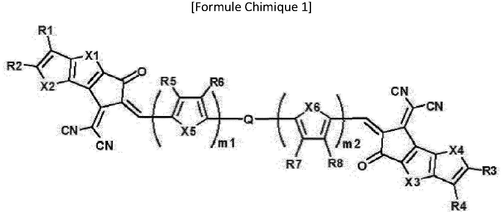 X1 à X6 sont identiques les uns aux autres ou différents les uns des autres, et sont chacun indépendamment CRR', NR, O, SiRR', PR, S, GeRR', Se, ou Te,R1 à R8, R, et R' sont identiques les uns aux autres ou différents les uns des autres, et sont chacun indépendamment un hydrogène; un deutérium ; un groupe halogène ; un groupe hydroxy ; un groupe alkyle substitué ou non substitué ; ou un groupe alcoxy substitué ou non substitué,m1 et m2 sont chacun 0 ou 1,Q est une structure représentée par l'une quelconque des Formules Chimiques A à C suivantes,dans les Formules Chimiques A à C,
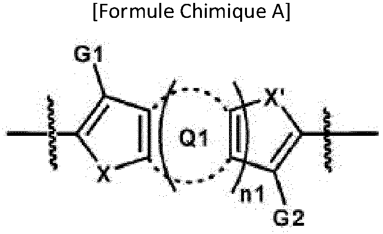

 X, X', X", et X"' sont identiques les uns aux autres ou différents les uns des autres, et sont chacun indépendamment S ou Se,Y1 est CR"R"' ou NR",G1 à G6, R", et R"' sont identiques les uns aux autres ou différents les uns des autres, et sont chacun indépendamment un hydrogène; un deutérium ; un groupe halogène ; un groupe hydroxy ; un groupe alkyle substitué ou non substitué ; un groupe alcoxy substitué ou non substitué ; un groupe aryle substitué ou non substitué ; ou un groupe hétéroaryle substitué ou non substitué,Q1 et Q2 sont identiques les uns aux autres ou différents les uns des autres, et sont chacun indépendamment un cycle substitué ou non substitué,g3 et g4 sont chacun un nombre entier allant de 1 à 3,n1 et n2 sont chacun un nombre entier allant de 1 à 5,quand g3, g4, n1, et n2 sont chacun 2 ou plus, deux ou plus de deux structures entre parenthèses sont identiques les unes aux autres ou différentes les unes des autres, et
- Composé hétérocyclique selon la revendication 1, dans lequel Q1 et Q2 sont identiques l'un à l'autre ou différents l'un de l'autre, et sont chacun indépendamment un cycle aromatique substitué ou non substitué ; ou un hétérocycle substitué ou non substitué.
- Composé hétérocyclique selon la revendication 1, dans lequel la Formule Chimique 1 est représentée par l'une quelconque des Formules Chimiques 1-1 à 1-3 suivantes :


 les définitions de X1 à X4, R1 à R8, m1, et m2 sont les mêmes que celles définies dans la Formule Chimique 1,les définitions de Q1, X, X', n1, G1, et G2 sont les mêmes que celles définies dans la Formule Chimique A,les définitions de Y1, G3, G4, g3, et g4 sont les mêmes que celles définies dans la Formule Chimique B, etles définitions de Q2, X", X"', n2, G5, et G6 sont les mêmes que celles définies dans la Formule Chimique C.
 - Composé hétérocyclique selon la revendication 1, dans lequel la Formule Chimique 1 est représentée par l'une quelconque des Formules Chimiques 1-4 à 1-15 suivantes :


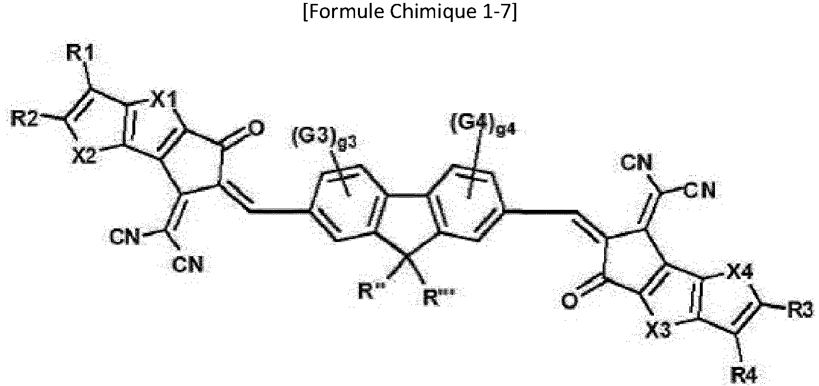


 les définitions de X1 à X4 et R1 à R8 sont les mêmes que celles définies dans la Formule Chimique 1,les définitions de X, X', G1, et G2 sont les mêmes que celles définies dans la Formule Chimique A,les définitions de G3, G4, g3, et g4 sont les mêmes que celles définies dans la Formule Chimique B,les définitions de X", X"', G5, et G6 sont les mêmes que celles définies dans la Formule Chimique C,X11 à X14 sont identiques les uns aux autres ou différents les uns des autres, et sont chacun indépendamment S ou Se,G101 à G123, R", et R"' sont identiques les uns aux autres ou différents les uns des autres, et sont chacun indépendamment un hydrogène ; un deutérium ; un groupe halogène ; un groupe hydroxy ; un groupe alkyle substitué ou non substitué ; un groupe alcoxy substitué ou non substitué ; un groupe aryle substitué ou non substitué ; ou un groupe hétéroaryle substitué ou non substitué,g105, g110, g111, g116, et g117 sont chacun 1 ou 2, etquand g105, g110, g111, g116, et g117 sont chacun 2, deux structures entre parenthèses sont identiques l'une à l'autre ou différentes l'une de l'autre.
 - Composé hétérocyclique selon la revendication 1, dans lequel la Formule Chimique 1 est représentée par l'une quelconque des Formules Chimiques 1-16 à 1-29 suivantes :


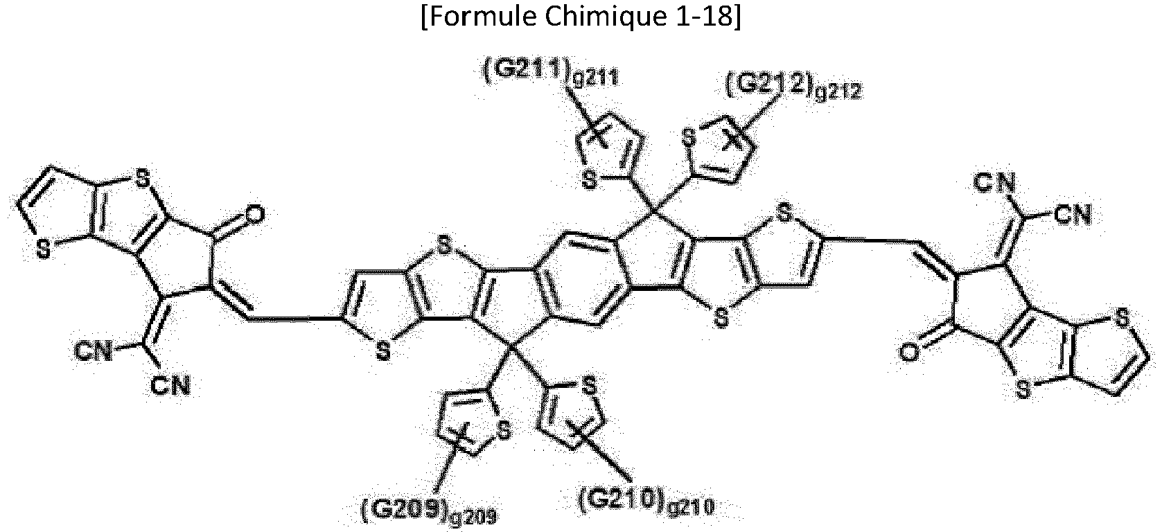


 R5 à R8 sont identiques les uns aux autres ou différents les uns des autres, et sont chacun indépendamment un hydrogène; un groupe alkyle substitué ou non substitué; ou un groupe alcoxy substitué ou non substitué,G120, G121, et G201 à G222 sont identiques les uns aux autres ou différents les uns des autres, et sont chacun indépendamment un hydrogène ; un groupe halogène ; un groupe alkyle substitué ou non substitué ; ou un groupe thioalcoxy substitué ou non substitué,R" et R"' sont identiques les uns aux autres ou différents les uns des autres, et sont chacun indépendamment un groupe alkyle substitué ou non substitué,g201 à g208, g213 à g216, et g219 à g222 sont chacun un nombre entier allant de 1 à 5,g209 à g212, g217, et g218 sont chacun un nombre entier allant de 1 à 3, etquand g201 à g222 sont chacun 2 ou plus, deux ou plus de deux structures entre parenthèses sont identiques les unes aux autres ou différentes les unes des autres.
 - Composé hétérocyclique selon la revendication 1, dans lequel la Formule Chimique 1 est sélectionnée parmi les composés suivants :


- Dispositif électronique organique comprenant :une première électrode ;une seconde électrode disposée pour faire face à la première électrode ; etune couche de matériau organique comprenant une ou plusieurs couches disposées entre la première électrode et la seconde électrode,dans lequel une ou plusieurs couches de la couche de matériau organique comprennent le composé hétérocyclique de l'une quelconque des revendications 1 à 6.
- Dispositif électronique organique selon la revendication 7, dans lequel la couche de matériau organique comprend une couche photoactive,
la couche photoactive présente une structure de film mince bicouche comprenant une couche de matériau organique de type n et une couche de matériau organique de type p, et
la couche de matériau organique de type n comprend le composé hétérocyclique. - Dispositif électronique organique selon la revendication 7, dans lequel la couche de matériau organique comprend une couche photoactive,
la couche photoactive comprend un matériau donneur d'électrons et un matériau accepteur d'électrons, et
le matériau accepteur d'électrons comprend le composé hétérocyclique. - Dispositif électronique organique selon la revendication 9, dans lequel le donneur d'électrons et l'accepteur d'électrons constituent une hétérojonction en volume (BHJ).
- Dispositif électronique organique selon la revendication 7, dans lequel le dispositif électronique organique est sélectionné dans le groupe consistant en un dispositif photoélectrique organique, un transistor organique, une cellule solaire organique, et un dispositif électroluminescent organique.
- Capteur organique d'image comprenant le dispositif électronique organique selon la revendication 7.
- Dispositif électronique comprenant le capteur organique d'image selon la revendication 12.
Applications Claiming Priority (3)
| Application Number | Priority Date | Filing Date | Title |
|---|---|---|---|
| KR20170064097 | 2017-05-24 | ||
| KR1020170133228A KR101902129B1 (ko) | 2017-05-24 | 2017-10-13 | 헤테로환 화합물 및 이를 포함하는 유기 전자 소자 |
| PCT/KR2018/001325 WO2018216880A1 (fr) | 2017-05-24 | 2018-01-31 | Composé hétérocyclique et dispositif électronique organique le comprenant |
Publications (3)
| Publication Number | Publication Date |
|---|---|
| EP3473627A1 EP3473627A1 (fr) | 2019-04-24 |
| EP3473627A4 EP3473627A4 (fr) | 2019-09-04 |
| EP3473627B1 true EP3473627B1 (fr) | 2020-03-18 |
Family
ID=63721367
Family Applications (1)
| Application Number | Title | Priority Date | Filing Date |
|---|---|---|---|
| EP18805836.6A Active EP3473627B1 (fr) | 2017-05-24 | 2018-01-31 | Composé hétérocyclique et dispositif électronique organique le comprenant |
Country Status (7)
| Country | Link |
|---|---|
| US (1) | US11008343B2 (fr) |
| EP (1) | EP3473627B1 (fr) |
| JP (1) | JP6635530B2 (fr) |
| KR (1) | KR101902129B1 (fr) |
| CN (1) | CN109476679B (fr) |
| TW (1) | TWI671304B (fr) |
| WO (1) | WO2018216880A1 (fr) |
Families Citing this family (11)
| Publication number | Priority date | Publication date | Assignee | Title |
|---|---|---|---|---|
| JP6786769B2 (ja) * | 2017-10-23 | 2020-11-18 | エルジー・ケム・リミテッド | ヘテロ環化合物およびこれを含む有機電子素子 |
| KR102428979B1 (ko) * | 2018-01-18 | 2022-08-03 | 주식회사 엘지화학 | 헤테로환 화합물 및 이를 포함하는 유기 전자 소자 |
| CN110964036A (zh) * | 2018-12-27 | 2020-04-07 | 深圳睿迅有机太阳能有限公司 | 基于含氮六并稠环单元的共轭分子及其制备方法和应用 |
| KR102629144B1 (ko) * | 2019-02-14 | 2024-01-24 | 주식회사 엘지화학 | 헤테로환 화합물 및 이를 포함하는 유기 전자 소자 |
| CN109824694B (zh) * | 2019-03-19 | 2022-01-21 | 苏州大学 | 基于苯并二呋喃的七并稠环单元的a-d-a共轭分子及其制备方法和应用 |
| KR102635061B1 (ko) * | 2019-03-20 | 2024-02-07 | 주식회사 엘지화학 | 헤테로환 화합물 및 이를 포함하는 유기 전자 소자 |
| KR102639496B1 (ko) * | 2019-04-09 | 2024-02-21 | 주식회사 엘지화학 | 헤테로환 화합물 및 이를 포함하는 유기 전자 소자 |
| TWI795639B (zh) * | 2019-04-12 | 2023-03-11 | 天光材料科技股份有限公司 | 有機半導體材料及應用其之有機光電元件 |
| CN110256459A (zh) * | 2019-05-28 | 2019-09-20 | 苏州大学 | 一种含烷基苯共轭侧链的有机小分子及其制备方法和应用 |
| EP3812383A1 (fr) * | 2019-10-24 | 2021-04-28 | Sumitomo Chemical Co., Ltd | Composé |
| CN113173929B (zh) * | 2021-04-07 | 2024-04-23 | 香港科技大学深圳研究院 | 基于芴或茚并芴及噻吩端基大带隙受体材料、制备方法及应用 |
Family Cites Families (13)
| Publication number | Priority date | Publication date | Assignee | Title |
|---|---|---|---|---|
| US5331183A (en) | 1992-08-17 | 1994-07-19 | The Regents Of The University Of California | Conjugated polymer - acceptor heterojunctions; diodes, photodiodes, and photovoltaic cells |
| WO2011022530A2 (fr) | 2009-08-19 | 2011-02-24 | Federal-Mogul Corporation | Ensemble joint de culasse |
| WO2013018951A1 (fr) | 2011-08-03 | 2013-02-07 | 포항공과대학교 산학협력단 | Polymère conducteur comprenant du 3,6-carbazole et pile photovoltaïque organique l'utilisant |
| KR101595919B1 (ko) | 2013-08-30 | 2016-02-29 | 한국과학기술연구원 | 전도성 유기 반도체 화합물 및 이를 포함하는 유기태양전지 |
| CN104557968B (zh) * | 2013-10-29 | 2017-04-05 | 中国科学院化学研究所 | 基于二噻吩并引达省的a‑d‑a共轭分子及其制备方法和应用 |
| EP2903047A1 (fr) | 2014-01-31 | 2015-08-05 | Ecole Polytechnique Fédérale de Lausanne (EPFL) | Matériau de transport de trous et d'absorption de lumière pour cellules solaires à l'état solide |
| KR101769665B1 (ko) | 2014-03-27 | 2017-08-21 | 주식회사 엘지화학 | 헤테로환 화합물 및 이를 포함하는 유기 태양 전지 |
| KR101677841B1 (ko) * | 2014-04-21 | 2016-11-18 | 주식회사 엘지화학 | 헤테로환 화합물 및 이를 포함하는 유기 태양 전지 |
| CN107531731B (zh) | 2015-04-20 | 2021-02-19 | 株式会社Lg化学 | 杂环化合物和包含其的有机太阳能电池 |
| CN106883247B (zh) | 2017-02-24 | 2019-05-24 | 武汉大学 | 基于噻吩并环戊二酮衍生物的a-d-a共轭分子及其制备方法 |
| CN107652304B (zh) * | 2017-09-28 | 2019-08-20 | 国家纳米科学中心 | 一种稠环非富勒烯受体材料及其制备方法与应用 |
| JP6786769B2 (ja) * | 2017-10-23 | 2020-11-18 | エルジー・ケム・リミテッド | ヘテロ環化合物およびこれを含む有機電子素子 |
| WO2018099492A2 (fr) * | 2017-12-21 | 2018-06-07 | Merck Patent Gmbh | Composés semi-conducteurs organiques |
-
2017
- 2017-10-13 KR KR1020170133228A patent/KR101902129B1/ko active IP Right Grant
-
2018
- 2018-01-31 EP EP18805836.6A patent/EP3473627B1/fr active Active
- 2018-01-31 WO PCT/KR2018/001325 patent/WO2018216880A1/fr unknown
- 2018-01-31 CN CN201880002864.3A patent/CN109476679B/zh active Active
- 2018-01-31 US US16/318,277 patent/US11008343B2/en active Active
- 2018-01-31 JP JP2018567050A patent/JP6635530B2/ja active Active
- 2018-02-07 TW TW107104297A patent/TWI671304B/zh active
Non-Patent Citations (1)
| Title |
|---|
| None * |
Also Published As
| Publication number | Publication date |
|---|---|
| US20190284210A1 (en) | 2019-09-19 |
| EP3473627A1 (fr) | 2019-04-24 |
| CN109476679A (zh) | 2019-03-15 |
| CN109476679B (zh) | 2022-01-11 |
| TWI671304B (zh) | 2019-09-11 |
| JP2019521997A (ja) | 2019-08-08 |
| EP3473627A4 (fr) | 2019-09-04 |
| US11008343B2 (en) | 2021-05-18 |
| TW201900650A (zh) | 2019-01-01 |
| JP6635530B2 (ja) | 2020-01-29 |
| KR101902129B1 (ko) | 2018-09-28 |
| WO2018216880A1 (fr) | 2018-11-29 |
Similar Documents
| Publication | Publication Date | Title |
|---|---|---|
| EP3473627B1 (fr) | Composé hétérocyclique et dispositif électronique organique le comprenant | |
| US10644241B2 (en) | Polymer and organic solar cell comprising same | |
| EP3121211A1 (fr) | Polymère et cellule solaire organique le comprenant | |
| EP3018160B1 (fr) | Copolymère et cellule solaire organique le comprenant | |
| KR102106668B1 (ko) | 헤테로환 화합물 및 이를 포함하는 유기 전자 소자 | |
| KR102389997B1 (ko) | 헤테로환 화합물 및 이를 포함하는 유기 태양 전지 | |
| EP3620458B1 (fr) | Composé hétérocyclique et dispositif électronique organique le comprenant | |
| US11398603B2 (en) | Heterocyclic compound and organic electronic device comprising same | |
| US20200002468A1 (en) | Compound and Organic Solar Cell Comprising Same | |
| KR20200119046A (ko) | 헤테로환 화합물 및 이를 포함하는 유기 전자 소자 | |
| KR102441145B1 (ko) | 중합체, 이를 포함하는 조성물 및 이를 포함하는 유기 태양 전지 | |
| EP3557642B1 (fr) | Couche photoactive et cellule solaire organique la comprenant | |
| EP3553063B1 (fr) | Composé et cellule solaire organique le comprenant | |
| KR102083711B1 (ko) | 헤테로환 화합물 및 이를 포함하는 유기 전자 소자 | |
| EP3395853B1 (fr) | Copolymère et cellule solaire organique le comprenant | |
| KR20200004084A (ko) | 헤테로환 화합물, 이를 포함하는 조성물 및 이를 포함하는 유기 전자 소자 | |
| KR20180127788A (ko) | 헤테로환 화합물 및 이를 포함하는 유기 전자 소자 | |
| KR102610463B1 (ko) | 헤테로환 화합물, 이를 포함하는 유기 전자 소자 및 이를 이용한 유기 전자 소자의 제조 방법 | |
| KR102552045B1 (ko) | 헤테로환 화합물, 이를 포함하는 유기 전자 소자 및 이를 이용한 유기 전자 소자의 제조 방법 | |
| KR20200119612A (ko) | 헤테로환 화합물 및 이를 포함하는 유기 전자 소자 | |
| KR102601531B1 (ko) | 인돌린 유도체 및 이를 포함하는 유기 전자 소자 | |
| KR20210001222A (ko) | 유기 태양 전지의 유기물층용 조성물, 이를 이용한 유기 태양 전지의 제조방법 및 유기 태양 전지 | |
| KR20200013401A (ko) | 화합물 및 이를 포함하는 유기 전자 소자 |
Legal Events
| Date | Code | Title | Description |
|---|---|---|---|
| STAA | Information on the status of an ep patent application or granted ep patent |
Free format text: STATUS: THE INTERNATIONAL PUBLICATION HAS BEEN MADE |
|
| PUAI | Public reference made under article 153(3) epc to a published international application that has entered the european phase |
Free format text: ORIGINAL CODE: 0009012 |
|
| STAA | Information on the status of an ep patent application or granted ep patent |
Free format text: STATUS: REQUEST FOR EXAMINATION WAS MADE |
|
| 17P | Request for examination filed |
Effective date: 20190115 |
|
| AK | Designated contracting states |
Kind code of ref document: A1 Designated state(s): AL AT BE BG CH CY CZ DE DK EE ES FI FR GB GR HR HU IE IS IT LI LT LU LV MC MK MT NL NO PL PT RO RS SE SI SK SM TR |
|
| AX | Request for extension of the european patent |
Extension state: BA ME |
|
| A4 | Supplementary search report drawn up and despatched |
Effective date: 20190807 |
|
| RIC1 | Information provided on ipc code assigned before grant |
Ipc: C07D 495/04 20060101AFI20190801BHEP Ipc: H01L 51/46 20060101ALI20190801BHEP |
|
| RIC1 | Information provided on ipc code assigned before grant |
Ipc: C07D 495/04 20060101AFI20191002BHEP Ipc: H01L 51/46 20060101ALI20191002BHEP |
|
| GRAP | Despatch of communication of intention to grant a patent |
Free format text: ORIGINAL CODE: EPIDOSNIGR1 |
|
| STAA | Information on the status of an ep patent application or granted ep patent |
Free format text: STATUS: GRANT OF PATENT IS INTENDED |
|
| DAV | Request for validation of the european patent (deleted) | ||
| DAX | Request for extension of the european patent (deleted) | ||
| INTG | Intention to grant announced |
Effective date: 20191111 |
|
| GRAS | Grant fee paid |
Free format text: ORIGINAL CODE: EPIDOSNIGR3 |
|
| GRAA | (expected) grant |
Free format text: ORIGINAL CODE: 0009210 |
|
| STAA | Information on the status of an ep patent application or granted ep patent |
Free format text: STATUS: THE PATENT HAS BEEN GRANTED |
|
| AK | Designated contracting states |
Kind code of ref document: B1 Designated state(s): AL AT BE BG CH CY CZ DE DK EE ES FI FR GB GR HR HU IE IS IT LI LT LU LV MC MK MT NL NO PL PT RO RS SE SI SK SM TR |
|
| REG | Reference to a national code |
Ref country code: GB Ref legal event code: FG4D |
|
| REG | Reference to a national code |
Ref country code: AT Ref legal event code: REF Ref document number: 1245791 Country of ref document: AT Kind code of ref document: T Effective date: 20200415 Ref country code: IE Ref legal event code: FG4D |
|
| REG | Reference to a national code |
Ref country code: DE Ref legal event code: R096 Ref document number: 602018003165 Country of ref document: DE |
|
| PG25 | Lapsed in a contracting state [announced via postgrant information from national office to epo] |
Ref country code: RS Free format text: LAPSE BECAUSE OF FAILURE TO SUBMIT A TRANSLATION OF THE DESCRIPTION OR TO PAY THE FEE WITHIN THE PRESCRIBED TIME-LIMIT Effective date: 20200318 Ref country code: NO Free format text: LAPSE BECAUSE OF FAILURE TO SUBMIT A TRANSLATION OF THE DESCRIPTION OR TO PAY THE FEE WITHIN THE PRESCRIBED TIME-LIMIT Effective date: 20200618 Ref country code: FI Free format text: LAPSE BECAUSE OF FAILURE TO SUBMIT A TRANSLATION OF THE DESCRIPTION OR TO PAY THE FEE WITHIN THE PRESCRIBED TIME-LIMIT Effective date: 20200318 |
|
| REG | Reference to a national code |
Ref country code: NL Ref legal event code: MP Effective date: 20200318 |
|
| PG25 | Lapsed in a contracting state [announced via postgrant information from national office to epo] |
Ref country code: SE Free format text: LAPSE BECAUSE OF FAILURE TO SUBMIT A TRANSLATION OF THE DESCRIPTION OR TO PAY THE FEE WITHIN THE PRESCRIBED TIME-LIMIT Effective date: 20200318 Ref country code: BG Free format text: LAPSE BECAUSE OF FAILURE TO SUBMIT A TRANSLATION OF THE DESCRIPTION OR TO PAY THE FEE WITHIN THE PRESCRIBED TIME-LIMIT Effective date: 20200618 Ref country code: LV Free format text: LAPSE BECAUSE OF FAILURE TO SUBMIT A TRANSLATION OF THE DESCRIPTION OR TO PAY THE FEE WITHIN THE PRESCRIBED TIME-LIMIT Effective date: 20200318 Ref country code: GR Free format text: LAPSE BECAUSE OF FAILURE TO SUBMIT A TRANSLATION OF THE DESCRIPTION OR TO PAY THE FEE WITHIN THE PRESCRIBED TIME-LIMIT Effective date: 20200619 Ref country code: HR Free format text: LAPSE BECAUSE OF FAILURE TO SUBMIT A TRANSLATION OF THE DESCRIPTION OR TO PAY THE FEE WITHIN THE PRESCRIBED TIME-LIMIT Effective date: 20200318 |
|
| REG | Reference to a national code |
Ref country code: LT Ref legal event code: MG4D |
|
| PG25 | Lapsed in a contracting state [announced via postgrant information from national office to epo] |
Ref country code: NL Free format text: LAPSE BECAUSE OF FAILURE TO SUBMIT A TRANSLATION OF THE DESCRIPTION OR TO PAY THE FEE WITHIN THE PRESCRIBED TIME-LIMIT Effective date: 20200318 |
|
| PG25 | Lapsed in a contracting state [announced via postgrant information from national office to epo] |
Ref country code: SK Free format text: LAPSE BECAUSE OF FAILURE TO SUBMIT A TRANSLATION OF THE DESCRIPTION OR TO PAY THE FEE WITHIN THE PRESCRIBED TIME-LIMIT Effective date: 20200318 Ref country code: IS Free format text: LAPSE BECAUSE OF FAILURE TO SUBMIT A TRANSLATION OF THE DESCRIPTION OR TO PAY THE FEE WITHIN THE PRESCRIBED TIME-LIMIT Effective date: 20200718 Ref country code: RO Free format text: LAPSE BECAUSE OF FAILURE TO SUBMIT A TRANSLATION OF THE DESCRIPTION OR TO PAY THE FEE WITHIN THE PRESCRIBED TIME-LIMIT Effective date: 20200318 Ref country code: LT Free format text: LAPSE BECAUSE OF FAILURE TO SUBMIT A TRANSLATION OF THE DESCRIPTION OR TO PAY THE FEE WITHIN THE PRESCRIBED TIME-LIMIT Effective date: 20200318 Ref country code: PT Free format text: LAPSE BECAUSE OF FAILURE TO SUBMIT A TRANSLATION OF THE DESCRIPTION OR TO PAY THE FEE WITHIN THE PRESCRIBED TIME-LIMIT Effective date: 20200812 Ref country code: CZ Free format text: LAPSE BECAUSE OF FAILURE TO SUBMIT A TRANSLATION OF THE DESCRIPTION OR TO PAY THE FEE WITHIN THE PRESCRIBED TIME-LIMIT Effective date: 20200318 Ref country code: SM Free format text: LAPSE BECAUSE OF FAILURE TO SUBMIT A TRANSLATION OF THE DESCRIPTION OR TO PAY THE FEE WITHIN THE PRESCRIBED TIME-LIMIT Effective date: 20200318 Ref country code: EE Free format text: LAPSE BECAUSE OF FAILURE TO SUBMIT A TRANSLATION OF THE DESCRIPTION OR TO PAY THE FEE WITHIN THE PRESCRIBED TIME-LIMIT Effective date: 20200318 |
|
| REG | Reference to a national code |
Ref country code: AT Ref legal event code: MK05 Ref document number: 1245791 Country of ref document: AT Kind code of ref document: T Effective date: 20200318 |
|
| REG | Reference to a national code |
Ref country code: DE Ref legal event code: R097 Ref document number: 602018003165 Country of ref document: DE |
|
| PLBE | No opposition filed within time limit |
Free format text: ORIGINAL CODE: 0009261 |
|
| STAA | Information on the status of an ep patent application or granted ep patent |
Free format text: STATUS: NO OPPOSITION FILED WITHIN TIME LIMIT |
|
| PG25 | Lapsed in a contracting state [announced via postgrant information from national office to epo] |
Ref country code: IT Free format text: LAPSE BECAUSE OF FAILURE TO SUBMIT A TRANSLATION OF THE DESCRIPTION OR TO PAY THE FEE WITHIN THE PRESCRIBED TIME-LIMIT Effective date: 20200318 Ref country code: DK Free format text: LAPSE BECAUSE OF FAILURE TO SUBMIT A TRANSLATION OF THE DESCRIPTION OR TO PAY THE FEE WITHIN THE PRESCRIBED TIME-LIMIT Effective date: 20200318 Ref country code: ES Free format text: LAPSE BECAUSE OF FAILURE TO SUBMIT A TRANSLATION OF THE DESCRIPTION OR TO PAY THE FEE WITHIN THE PRESCRIBED TIME-LIMIT Effective date: 20200318 Ref country code: AT Free format text: LAPSE BECAUSE OF FAILURE TO SUBMIT A TRANSLATION OF THE DESCRIPTION OR TO PAY THE FEE WITHIN THE PRESCRIBED TIME-LIMIT Effective date: 20200318 |
|
| 26N | No opposition filed |
Effective date: 20201221 |
|
| PG25 | Lapsed in a contracting state [announced via postgrant information from national office to epo] |
Ref country code: PL Free format text: LAPSE BECAUSE OF FAILURE TO SUBMIT A TRANSLATION OF THE DESCRIPTION OR TO PAY THE FEE WITHIN THE PRESCRIBED TIME-LIMIT Effective date: 20200318 |
|
| PG25 | Lapsed in a contracting state [announced via postgrant information from national office to epo] |
Ref country code: SI Free format text: LAPSE BECAUSE OF FAILURE TO SUBMIT A TRANSLATION OF THE DESCRIPTION OR TO PAY THE FEE WITHIN THE PRESCRIBED TIME-LIMIT Effective date: 20200318 |
|
| PG25 | Lapsed in a contracting state [announced via postgrant information from national office to epo] |
Ref country code: MC Free format text: LAPSE BECAUSE OF FAILURE TO SUBMIT A TRANSLATION OF THE DESCRIPTION OR TO PAY THE FEE WITHIN THE PRESCRIBED TIME-LIMIT Effective date: 20200318 |
|
| REG | Reference to a national code |
Ref country code: CH Ref legal event code: PL |
|
| PG25 | Lapsed in a contracting state [announced via postgrant information from national office to epo] |
Ref country code: LU Free format text: LAPSE BECAUSE OF NON-PAYMENT OF DUE FEES Effective date: 20210131 |
|
| REG | Reference to a national code |
Ref country code: BE Ref legal event code: MM Effective date: 20210131 |
|
| PG25 | Lapsed in a contracting state [announced via postgrant information from national office to epo] |
Ref country code: LI Free format text: LAPSE BECAUSE OF NON-PAYMENT OF DUE FEES Effective date: 20210131 Ref country code: CH Free format text: LAPSE BECAUSE OF NON-PAYMENT OF DUE FEES Effective date: 20210131 |
|
| PG25 | Lapsed in a contracting state [announced via postgrant information from national office to epo] |
Ref country code: IE Free format text: LAPSE BECAUSE OF NON-PAYMENT OF DUE FEES Effective date: 20210131 |
|
| PG25 | Lapsed in a contracting state [announced via postgrant information from national office to epo] |
Ref country code: BE Free format text: LAPSE BECAUSE OF NON-PAYMENT OF DUE FEES Effective date: 20210131 |
|
| PG25 | Lapsed in a contracting state [announced via postgrant information from national office to epo] |
Ref country code: CY Free format text: LAPSE BECAUSE OF FAILURE TO SUBMIT A TRANSLATION OF THE DESCRIPTION OR TO PAY THE FEE WITHIN THE PRESCRIBED TIME-LIMIT Effective date: 20200318 |
|
| PG25 | Lapsed in a contracting state [announced via postgrant information from national office to epo] |
Ref country code: HU Free format text: LAPSE BECAUSE OF FAILURE TO SUBMIT A TRANSLATION OF THE DESCRIPTION OR TO PAY THE FEE WITHIN THE PRESCRIBED TIME-LIMIT; INVALID AB INITIO Effective date: 20180131 |
|
| PGFP | Annual fee paid to national office [announced via postgrant information from national office to epo] |
Ref country code: GB Payment date: 20231220 Year of fee payment: 7 |
|
| PGFP | Annual fee paid to national office [announced via postgrant information from national office to epo] |
Ref country code: FR Payment date: 20231222 Year of fee payment: 7 |
|
| PG25 | Lapsed in a contracting state [announced via postgrant information from national office to epo] |
Ref country code: MK Free format text: LAPSE BECAUSE OF FAILURE TO SUBMIT A TRANSLATION OF THE DESCRIPTION OR TO PAY THE FEE WITHIN THE PRESCRIBED TIME-LIMIT Effective date: 20200318 |
|
| PGFP | Annual fee paid to national office [announced via postgrant information from national office to epo] |
Ref country code: DE Payment date: 20231220 Year of fee payment: 7 |