EP3427455B1 - Intelligent equalization for a three-transmitter multi-phase system - Google Patents
Intelligent equalization for a three-transmitter multi-phase system Download PDFInfo
- Publication number
- EP3427455B1 EP3427455B1 EP17712639.8A EP17712639A EP3427455B1 EP 3427455 B1 EP3427455 B1 EP 3427455B1 EP 17712639 A EP17712639 A EP 17712639A EP 3427455 B1 EP3427455 B1 EP 3427455B1
- Authority
- EP
- European Patent Office
- Prior art keywords
- level
- output signal
- mid
- transmitter
- low
- Prior art date
- Legal status (The legal status is an assumption and is not a legal conclusion. Google has not performed a legal analysis and makes no representation as to the accuracy of the status listed.)
- Active
Links
Images


Classifications
-
- H—ELECTRICITY
- H04—ELECTRIC COMMUNICATION TECHNIQUE
- H04L—TRANSMISSION OF DIGITAL INFORMATION, e.g. TELEGRAPHIC COMMUNICATION
- H04L25/00—Baseband systems
- H04L25/38—Synchronous or start-stop systems, e.g. for Baudot code
- H04L25/40—Transmitting circuits; Receiving circuits
- H04L25/49—Transmitting circuits; Receiving circuits using code conversion at the transmitter; using predistortion; using insertion of idle bits for obtaining a desired frequency spectrum; using three or more amplitude levels ; Baseband coding techniques specific to data transmission systems
- H04L25/4917—Transmitting circuits; Receiving circuits using code conversion at the transmitter; using predistortion; using insertion of idle bits for obtaining a desired frequency spectrum; using three or more amplitude levels ; Baseband coding techniques specific to data transmission systems using multilevel codes
-
- H—ELECTRICITY
- H04—ELECTRIC COMMUNICATION TECHNIQUE
- H04L—TRANSMISSION OF DIGITAL INFORMATION, e.g. TELEGRAPHIC COMMUNICATION
- H04L25/00—Baseband systems
- H04L25/02—Details ; arrangements for supplying electrical power along data transmission lines
- H04L25/0264—Arrangements for coupling to transmission lines
- H04L25/0272—Arrangements for coupling to multiple lines, e.g. for differential transmission
-
- H—ELECTRICITY
- H03—ELECTRONIC CIRCUITRY
- H03K—PULSE TECHNIQUE
- H03K5/00—Manipulating of pulses not covered by one of the other main groups of this subclass
- H03K5/153—Arrangements in which a pulse is delivered at the instant when a predetermined characteristic of an input signal is present or at a fixed time interval after this instant
-
- H—ELECTRICITY
- H04—ELECTRIC COMMUNICATION TECHNIQUE
- H04B—TRANSMISSION
- H04B7/00—Radio transmission systems, i.e. using radiation field
- H04B7/02—Diversity systems; Multi-antenna system, i.e. transmission or reception using multiple antennas
- H04B7/04—Diversity systems; Multi-antenna system, i.e. transmission or reception using multiple antennas using two or more spaced independent antennas
- H04B7/06—Diversity systems; Multi-antenna system, i.e. transmission or reception using multiple antennas using two or more spaced independent antennas at the transmitting station
- H04B7/0613—Diversity systems; Multi-antenna system, i.e. transmission or reception using multiple antennas using two or more spaced independent antennas at the transmitting station using simultaneous transmission
- H04B7/0682—Diversity systems; Multi-antenna system, i.e. transmission or reception using multiple antennas using two or more spaced independent antennas at the transmitting station using simultaneous transmission using phase diversity (e.g. phase sweeping)
-
- H—ELECTRICITY
- H04—ELECTRIC COMMUNICATION TECHNIQUE
- H04L—TRANSMISSION OF DIGITAL INFORMATION, e.g. TELEGRAPHIC COMMUNICATION
- H04L25/00—Baseband systems
- H04L25/02—Details ; arrangements for supplying electrical power along data transmission lines
- H04L25/03—Shaping networks in transmitter or receiver, e.g. adaptive shaping networks
- H04L25/03006—Arrangements for removing intersymbol interference
- H04L25/03343—Arrangements at the transmitter end
-
- H—ELECTRICITY
- H04—ELECTRIC COMMUNICATION TECHNIQUE
- H04L—TRANSMISSION OF DIGITAL INFORMATION, e.g. TELEGRAPHIC COMMUNICATION
- H04L25/00—Baseband systems
- H04L25/02—Details ; arrangements for supplying electrical power along data transmission lines
- H04L25/03—Shaping networks in transmitter or receiver, e.g. adaptive shaping networks
- H04L25/03878—Line equalisers; line build-out devices
-
- H—ELECTRICITY
- H04—ELECTRIC COMMUNICATION TECHNIQUE
- H04L—TRANSMISSION OF DIGITAL INFORMATION, e.g. TELEGRAPHIC COMMUNICATION
- H04L25/00—Baseband systems
- H04L25/02—Details ; arrangements for supplying electrical power along data transmission lines
- H04L25/14—Channel dividing arrangements, i.e. in which a single bit stream is divided between several baseband channels and reassembled at the receiver
-
- H—ELECTRICITY
- H04—ELECTRIC COMMUNICATION TECHNIQUE
- H04L—TRANSMISSION OF DIGITAL INFORMATION, e.g. TELEGRAPHIC COMMUNICATION
- H04L25/00—Baseband systems
- H04L25/38—Synchronous or start-stop systems, e.g. for Baudot code
- H04L25/40—Transmitting circuits; Receiving circuits
- H04L25/49—Transmitting circuits; Receiving circuits using code conversion at the transmitter; using predistortion; using insertion of idle bits for obtaining a desired frequency spectrum; using three or more amplitude levels ; Baseband coding techniques specific to data transmission systems
- H04L25/4917—Transmitting circuits; Receiving circuits using code conversion at the transmitter; using predistortion; using insertion of idle bits for obtaining a desired frequency spectrum; using three or more amplitude levels ; Baseband coding techniques specific to data transmission systems using multilevel codes
- H04L25/4923—Transmitting circuits; Receiving circuits using code conversion at the transmitter; using predistortion; using insertion of idle bits for obtaining a desired frequency spectrum; using three or more amplitude levels ; Baseband coding techniques specific to data transmission systems using multilevel codes using ternary codes
Definitions
- This application relates to a three-transmitter multi-phase system, and more particularly to a three-phase transmitter multi-phase system with mid-level adaptive equalization.
- a SERDES transmitter serializes a multi-bit word into a series of corresponding bits for transmission to a receiver. There can then be no such skew between adjacent bits on a multi-wire bus since a single transmission line (which may be differential) is used in a SERDES system.
- the SERDES receiver deserializes the received serial bit stream into the original word.
- the SERDES transmission line and the receiver load introduce distortion as the data transmission rate exceeds, for example, 10 GHz.
- Adjacent bits in the serial bit stream then begin to interfere with each other. Complicated equalizing schemes become necessary to fight the resulting inter-symbol interference and thus it becomes difficult to push SERDES data transmission rates ever higher.
- a three-phase signaling protocol has been developed in which three transmitters drive three separate transmission lines.
- one transmitter drives it output signal to a high voltage
- another transmitter drives its output signal to a mid-level voltage
- a remaining transmitter drives its output signal to a low voltage.
- the high voltage transmitter and low voltage transmitter may be deemed to form an active pair. From a set of three transmitters, there are three distinct pairs of transmitters that can be active. Within each pair, there are two possibilities depending upon which transmitter is high versus which transmitter is low. There are thus six distinct combinations of output signals in a three-transmitter multi-phase system. Each distinct combination of output signals may be denoted as a multi-phase symbol. Since there are six possible symbols, each transmitted symbol represents 2.5 bits. In this fashion, data transmission speeds may be more than doubled over binary transmission at the same symbol rate using a single channel, albeit at the cost of increased power consumption.
- a frontend circuit decodes the received transmitter output signals to produce the corresponding binary symbol.
- the six different symbols may be represented by six binary words: [100], [010], [001], [110], [101], and [011].
- the bits in these symbols may be represented by the binary variables A, B, and C.
- no self-transition is allowed. For example, suppose the symbol [001] had just been received. The subsequent symbol cannot be [001] as this would violate the ban against self-transition. In this fashion, a clock can be extracted from every received symbol from the guaranteed binary transition of at least one of the binary signals.
- inter-symbol interference ISI
- SERDES SERDES
- inter-symbol interference must still be addressed for a three-transmitter multi-phase system as the data rate is increased ever higher.
- conventional equalization techniques are adapted from traditional two-level (high voltage for a binary one and low voltage for a binary zero) signaling.
- Application of such traditional equalization techniques to a three-transmitter multi-phase system results in over-emphasis that worsens timing jitter and wastes power.
- a method for data communications includes determining a transition in signaling state of three wires of a communication link between a pair of consecutive symbols transmitted on the communication link, and enhancing or attenuating energy of a signal prior to the transition in signaling state of the three wires when the transition in signaling state includes a change in signaling state of a wire on which the signal is transmitted.
- Each symbol may define a different signaling state of the three wires of the communication link.
- two of the three wires are differentially encoded and the third wire is in a neutral state. Different wires are differentially encoded during transmission of consecutive symbols.
- a three-transmitter multi-phase system is provided with intelligent equalization that selectively emphasizes and de-emphasizes rising and falling edges for the mid-level transitions of transmitter output signals (transitions to or from the mid-level output voltage).
- a logic circuit controls the emphasis and de-emphasis depending upon the transition from a previous multi-phase symbol to a current multi-phase symbol.
- Each transmitter output signal transitions uniquely into a high voltage, mid-level voltage or a low voltage for each multi-phase symbol.
- the resulting selective emphasis and de-emphasis of just the mid-level transitions advantageously reduces power consumption compared to an application of traditional equalization while reducing data jitter.
- a three-transmitter multi-phase system is provided with an intelligent equalization technique.
- the equalization technique is denoted as "intelligent" as it is adaptive to the various transitions that are possible for each transmitter output signal. Some transitions (rising edges or falling edges) are emphasized whereas other types of transitions are actually de-emphasized. Moreover, some transitions are neither emphasized nor de-emphasized.
- the selective emphasis, de-emphasis, and the lack thereof may be better appreciated with regard to an example three-transmitter multi-phase system 100 shown in Figure 1 .
- An encoder 135 encodes an input data stream into consecutive multi-phase symbols.
- Each multi-phase symbol has three components, corresponding to the states for the output signals for a first transmitter 105, a second transmitter 110, and a third transmitter 115.
- Each transmitter drives a corresponding transmission line.
- First transmitter 105 drivers a first transmission line 120 with a transmitter output signal A whereas second transmitter 110 drives a second transmission line 125 with a transmitter output signal B.
- third transmitter 115 drives a third transmission line 130 with a transmitter output signal C.
- each output signal A, B, and C may be deemed to include a plurality of levels such as a high level, a mid-level and a low level. In a voltage-mode embodiment, these level are all voltage levels. Conversely, in a current-mode embodiment, the signal levels are all current levels.
- the selective emphasis and de-emphasis of rising and falling edges for the transmitter output signals disclosed herein involves the use of additional signal levels.
- the falling edge transition of an output signal from the mid-level to the low level may be emphasized by transitioning the output signal to a reduced mid-level that is less than the mid-level during an initial portion of a current multi-phase symbol. This output signal may then be returned to the mid-level for a remainder of the multi-phase symbol.
- the falling edge transition of an output signal from the mid-level to the low level may be selectively de-emphasized by first transitioning the output signal to an increased low level during the initial portion of the current multi-phase symbol. The increased low level is greater than the low level but less than the reduced mid-level.
- encoder 135 commands each transmitter to drive its transmission line with either a high voltage, a low voltage, or an intermediate voltage.
- VOH the high voltage
- VOL the low voltage
- VM the intermediate (mid-level) voltage
- VOH is higher than VOL.
- VM can equal (VOH-VOL)/2 or some other intermediate voltage that is less than VOH but greater than VOL.
- each multi-phase symbol for system 100 involves the driving of one of the transmission lines with VOH, another with VM, and a remaining one with VOL.
- encoder 135 can command a particular transmitter to pull up (PU) its output voltage towards VOH or pull down (PD) its output voltage towards VOL.
- encoder 135 can command a particular to mid-range (PM) its output voltage to VM.
- the PU, PD, and PM commands to first transmitter 105 are denoted as PU1, PD1, and PM1. Only one of these commands may be asserted for any given symbol transmission.
- encoder can assert one of a PU2, PD2, and PM2 command to second transmitter 110 and can assert one of a PU3, PD3, and PM3 command to third transmitter 115.
- the PM commands may be omitted in that an assertion of the PM command to a particular transmitter may be indicated by de-asserting both the corresponding PU command and the corresponding PD command.
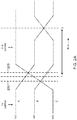
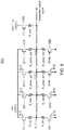
- FIG. 2A An example transition from one symbol to another (each symbol being represented by the VOH/VM/VOL states for the three transmitters) may be as shown in Figure 2A .
- the output signals of the three transmitters are designated as A, B, and C.
- Transmitter output signal A in the first symbol is at VOH whereas transmitter output signal B is at VM and transmitter output signal C is at VOL.
- transmitter output signal A transitions to VM
- transmitter output signal B transitions to VOL
- transmitter output signal C transitions to VOH.
- the boundary between the two symbols occurs at time t1.
- the transmitter output signal C crosses (equals) the transmitter output signal B at a time 200 that equals t1 - D, where D is a timing offset.
- the transmitter output signal A equals transmitter output signal C at a time 205 that equals t1 + D.
- the timing offsets increase data jitter. At relatively low symbol rates, such data jitter may be tolerable but becomes increasingly intolerable at higher symbol rates.
- both emphasis and de-emphasis may be applied as shown in Figure 2B .
- the falling edge transition of transmitter output signal A that transitions from VOH to VM is emphasized such that transmitter output A is initially discharged at an enhanced rate to a reduced intermediate voltage Vem2 that is lower than mid-level voltage Vm.
- this emphasis is released so that transmitter output signal A returns to its intended value of VM.
- the falling edge transition of transmitter output signal B transitioning from VM to VOL is de-emphasized such that transmitter output signal B is initially discharged at a de-emphasized rate to an increased low voltage VOL_EQ1 that is higher than VOL.
- transmitter output signal B can return to its intended value of VOL.
- An intersection at a time 210 of transmitter output signal C with transmitter output signal B is this delayed with respect to time 200 of Figure 2A .
- an intersection at a time 215 of transmitter output signal C with transmitter output signal A is advanced in time as compared to time 205 of Figure 2A . This is quite advantageous as the offset between times 210 and 215 from time t1 is reduced as compared to the timing offsets of times 200 and 205 from time t1.
- a logic circuit 140 controls the intelligent equalization such as for transmitter output signals A and B as discussed with regard to Figure 2B .
- Logic circuit 140 compares the intended VOH, VM, or VOL state for each transmitter output signal in a current symbol to the corresponding VOH, VM, or VOL state for each transmitter output signal in the preceding symbol to determine the applicable intelligent equalization.
- a memory 145 may store the previous states for the transmitter output signals. If logic circuit 140 detects a transition from VOH to VM for one transmitter output signal in conjunction with a transition from VM to VOL for another transmitter output signal, it controls the corresponding transmitters to apply the emphasis and de-emphasis discussed with regard to Figure 2B .
- Some example transmitter circuit implementations and corresponding control signals from logic circuit 140 will be discussed further below.
- Figure 2B is thus directed to the intelligent equalization of a transition from VOH to VM for one transmitter output signal in conjunction with a transition from VM to VOL for another transmitter output signal.
- An analogous intelligent equalization may be applied in a transition from VOL to VM for one transmitter output signal in conjunction with a transition from VM to VOH for another transmitter output signal.
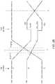
- An example transition between a first symbol and a second symbol is shown at a time t1 in Figure 3 .
- Transmitter output signal B equals VM in a first symbol and then transitions to VOH in a second symbol.
- a no-equalization rising edge 300 for transmitter output signal B is also shown in Figure 3 .
- Rising edge 300 intersects with a falling edge for transmitter output signal A at a time 301. There is a substantial timing offset between time 301 and the ideal symbol transition time of t1. To reduce this offset, the rising edge for transmitter output signal B is de-emphasized such that transmitter output signal B rises at a reduced rate to a reduced high voltage VOH_EQ2 that is less than VOH. This de-emphasis is released around the midpoint of the second symbol such that transmitter output signal B returns to its intended value of VOH for the latter portion of the second symbol.
- the de-emphasized rising edge for transmitter output B intersects with transmitter output signal A at a time 305 that is delayed with regard to time 301. The offset between time 305 and t1 is thus reduced as compared to the offset between time 301 and time t1.
- Transmitter output signal C equals VOL in the first symbol and transitions to VM in the second symbol.
- a rising edge 310 without equalization for transmitter output signal C is also shown in Figure 3 to better illustrate the advantages of the intelligent equalization.
- Rising edge 310 intersects with transmitter output signal A at time 315 that is delayed by the timing offset from the ideal symbol transition time of t1.
- the rising edge for transmitter output signal C is emphasized such that it rises at a faster rate to an enhanced midrange voltage Vem1 that is higher than VM.
- This emphasized rising edge for transmitter output signal C intersects with transmitter output signal A at a time 320 that is advanced compared to time 315.
- the offset between time 320 and time t1 is thus reduced as compared to the offset between time 315 and time t1.
- the resulting intelligent equalization for transmitter output signals B and C reduces the jitter in the transition from the first symbol to the second symbol.
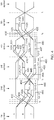
- a transmitter output signal remains at VOH for two consecutive symbols.
- a transmitter output signal remains at VOL for two consecutive symbols.
- the first symbol and a second symbol form the transition discussed with regard to Figures 2A and 2B .
- falling edges 400 and 405 for transmitter output signals A and B, respectively are produced with intelligent equalization whereas corresponding falling edges 410 and 415 are produced without any equalization.
- a fourth symbol and a fifth symbol form the transition discussed with regard to Figure 3 .
- rising edges 420 and 425 for transmitter output signals C and A, respectively are produced with intelligent equalization whereas corresponding rising edges 430 and 435 are produced without any equalization.
- transmitter output signal C In a transition from the second symbol to a third symbol, transmitter output signal C remains at VOH (without any equalization). Since at least two transmitter output signals must change state from one symbol to another so that a receiver may extract a clock signal, transmitter output signal B goes from VOL to VM in the transition from the second symbol to the third symbol whereas transmitter output signal A discharges from VM to VOL.
- a rising edge 440 for transmitter output signal B may thus be emphasized such that transmitter output signal B rises at an increased rate to the voltage Vem1 that is higher than VM for a first portion of the third symbol.
- a rising edge 445 for transmitter output signal B is also shown in Figure 4 to illustrate a no-equalization result.
- a falling edge 450 for transmitter output signal A may be emphasized such that transmitter output signal A falls at an enhanced rate to a voltage VOL_EQ1 that is lower than VOL.
- a falling edge 455 for transmitter output signal A illustrates a no-equalization result.
- emphasized edges 440 and 450 concern transitions between the midlevel voltage VM and VOL. As discussed previously, emphasizing such transitions does not consume as much power as emphasizing transitions between VOL and VOH yet still significantly reduces data jitter.
- transmitter output signal C is discharged to a voltage VOH_EQ2 that is lower than VOH for the duration of the third symbol. In this fashion, transmitter output signal C can be discharged more quickly in a subsequent symbol to either VM or VOL.
- transmitter output signal A In a transition from the third symbol to a fourth symbol, transmitter output signal A remains at VOL in the absence of any equalization. However, in the same transition with intelligent equalization, transmitter output signal A is charged to the voltage VOL_EQ1 (discussed with regard to Figure 2B ) that is higher than VOL for the duration of the third symbol. In this fashion, transmitter output signal A can be charged more quickly in a subsequent symbol to either VM or VOH. Since there must be a transition for the transmitter output signals in every symbol for clock extraction at the receiver, transmitter output signal B transitions from VM to VOH at the beginning of the fourth symbol in an embodiment without equalization through rising edge 460.
- An emphasized rising edge 465 represents the result with intelligent equalization such that transmitter output signal B rises at an enhanced rate the voltage VOH_EQ1 that is higher than VOH for a first portion of the fourth symbol.
- a falling edge for 470 for transmitter output signal C is emphasized such that transmitter output signal C falls to Vem2 (discussed with regard to Figure 2B ) for the first portion of the fourth symbol.
- a falling edge 475 illustrates the transition for transmitter output signal C without equalization. Note that the emphasis for edges 465 and 470 concern transitions between VM and VOH such that their emphasis does not consume significant power yet significantly reduces data jitter.
- transmitter output signal C transitions from VOH to VOL.
- transmitter output signal B transitions from VOL to VOH.
- Emphasizing such full-rail edges would consume power. Thus, it is "intelligent" for no emphasis to be applied to either of these edges. However, these edges may be emphasized in alternative embodiments.
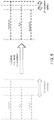
- the ideal transition times between the symbols in Figure 4 are denoted as times t1 through t5. These times are separated by the desired unit interval (UI). Without any equalization, it can be shown that a duration 480 of the second symbol equals U1 + D, where D is a time offset. But after the application of intelligent equalization, a duration 485 of the second symbol becomes UI + D - X, where X is the adjustment from the intelligent equalization. Similarly, it can be shown that a duration 490 of the third symbol is UI with intelligent equalization as is a duration 495 without intelligent equalization. In contrast, a duration 486 of the fourth symbol without equalization is UI - D. But a duration 487 of the fourth symbol with intelligent equalization is increased to UI - D + X so as to more closely match the ideal symbol interval of UI.
- the resulting advantageous adjustment of the various symbol durations by intelligent equalization towards the desired value of UI is summarized in Figure 5 .
- the application of intelligent equalization may also be denoted as an application of adaptive mid-level equalization since only the rising and falling edges from or to the mid-level voltage VM are either emphasized (or de-emphasized).
- the total UI variation without equalization is 2D whereas it is merely 2X after application of intelligent equalization. Since X is less than D, the resulting UI variation is thus significantly reduced, which reduces data jitter accordingly.
- logic circuit 140 and memory 145 comprise a means for means for selectively emphasizing a first falling edge for an output signal from a first one of the transmitters that is transitioning from the high voltage to the mid-level voltage and for selectively de-emphasizing a second falling edge for another output signal from a second one of the transmitters that is transitioning from the mid-level voltage to the low voltage.
- each transmitter 105, 110, and 115 discussed with regard to Figure 1 may be implemented as shown in Figure 6 for a transmitter 600.
- encoder 135 determines the VOH, VM, and VOL state for each transmitter. These states are the non-emphasized states discussed with regard to Figures 2B , 3 , and 4 for the transmitter output signals. For example, if the pull-up signal PU1 is asserted while corresponding pull-down signal PD1 and mid-level signal PM1 for transmitter 105 are de-asserted, corresponding transmitter output signal A is charged to VOH without equalization. In that case, transmitter output signals B and C must be uniquely assigned to either VM or VOL.
- encoder 135 may provide the corresponding control signals PU1, PD1, PM1, PU2, PD2, PM2, PU3, PD3, and PM3 to logic circuit 140. These same signals for the previous symbol are stored in memory 145 so that logic circuit 140 can compare the state for the previous symbol to the state for the current symbol to control the application of intelligent equalization accordingly.
- the control signals from logic circuit 140 to control the application of intelligent equalization depend upon the particular circuit implementation for each transmitter 105, 110, and 115.
- a plurality of voltage regulators may be used to provide a corresponding plurality of regulated voltage levels.
- a first linear dropout regulator LDO1, not illustrated
- a second LDO LDO2, not illustrated
- may provide a second drive voltage e.g., 0.5 * Vdrv).
- Transmitter 600 is thus configured to provide these "non-emphasized" voltage levels for the duration of a symbol (the conventional VOH, VM, and VOL levels).
- transmitter 600 includes an NMOS pull-up transistor 605 in series with a pull-up resistor R_up.
- the source of pull-up transistor 605 couples to the pull-up resistor R_up whereas its drain is charged to the power supply voltage Vdrv by LDO1.
- the pull-up resistor R_up couples to an output node 610 for providing the transmitter output signal.
- a pull-up signal PU (a corresponding one of signals PU1, PU2, and PU3 discussed with regard to Figure 1 ) drives the gate of pull-up transistor 605.
- the resistance of the pull-up resistor R_up along with an input resistance of the receiver (not illustrated) receiving the transmitter output signal forms a voltage divider that divides the power supply voltage Vdrv from LDO1 to charge output node 610 to VOH when pull-up signal PU is asserted.
- An analogous pull-down NMOS transistor 615 and pull-down resistor R_dn couple between output node 610 and ground.
- a pull-down signal PD (a corresponding one of signals PD1, PD2, and PD3 discussed with regard to Figure 1 ) drives the gate of pull-down transistor 615 such that output node 610 is discharged to VOL upon the assertion of pull-down signal PU.
- a serial combination of an NMOS mid-level transistor 620 and a mid-level resistor R_mid couple between a power supply node for the second LDO (LDO2) and output node 610.
- a mid-level signal PM (a corresponding one of signals PM1, PM2, and PM3) drives the gate of mid-level transistor 620 such that output node 610 is charged to VM upon the assertion of mid-level signal PM (in the absence of intelligent equalization).
- transmitter 600 includes an NMOS emphasized pull-up transistor 625 in series with an emphasized pull-up resistor R_eup that couples to output node 610.
- LDO1 drives a drain of emphasized pull-up transistor 625 with the power supply voltage Vdrv.
- An emphasized pull-up signal EPU1 drives the gate of transistor 625.
- the resistance of emphasized pull-up resistor R_eup is less than that of the pull-up resistor R_up such that when both PU and EPU1 are asserted, output node 610 is charged to VOH_EQ1. This emphasis may then be released midway through the symbol such that just pull-up transistor 605 remains on for the duration of the symbol to allow the transmitter output signal to drop to VOH.
- pull-down signal PD is asserted in conjunction with the assertion of an emphasized pull-down signal EPD1 that drives a gate of an NMOS emphasized pull-down transistor 640 in series with an emphasized pull-down resistor R_edn that couples to output node 610.
- Pull-down resistor R_dn and emphasized pull-down resistor R_edn are then coupled in parallel to output node 610 to produce a resistance that is less than a resistance for pull-down resistor R_dn.
- Output node 610 is then discharged to VOL_EQ2.
- emphasized pull-down signal EPD1 is released (de-asserted) so that output node 610 recovers to VOL.
- a control signal EPM1 is asserted to a voltage divider formed by a serial combination of an NMOS transistor 630, a resistor R_emid_up1, a resistor R_emid_dn1, and an NMOS transistor 635.
- Transistor 630 and resistor R_emid_up1 couple between the power supply node from LDO1 and output node 610.
- transistor 635 and resistor R_emid_dn1 couple between the power supply node 610 and ground.
- Control signal EPMl drives the gate transistors 630 and 635 to divide the power supply node Vdrv into the increased mid-level voltage Vem1.
- An analogous voltage divider including a pair of transistors 650 and 644, a resistor R_emid_up2, and a resistor R_emid_dn2 produce the reduced mid-level voltage Vem2 at output node 610 in response to the assertion of a control signal EMP2.
- Voltages VOH, VM, and VOL are the traditional (no equalization) voltage levels. Each of the voltage levels may be either emphasized or de-emphasized. VOH may thus be emphasized into VOH_EQ1. Similarly, VM may be emphasized into Vem1 whereas VOL may be emphasized into VOL_EQ2. Similarly, VOH may be de-emphasized into VOH_EQ2, VM may be de-emphasized into Vem2, and VOL de-emphasized into VOL_EO1.
- the method includes an act 800 of encoding an input data signal into a current command corresponding to a current one of the successive multi-phase symbols.
- Encoder 135 encoding the input data stream into the commands (e.g., PU1, PD1, PM1, etc.) corresponding to the various multi-phase symbols is an example of act 800.
- the method further includes an act 805 of comparing the current command to a previous state for an output signal from each of the three transmitters during a preceding one of the successive multi-phase symbols to detect when the current command commands a mid-level one of the transmitters to transition its output signal from a high-level to a mid-level and commands a low-level one of the transmitters to transition its output signal from the mid-level to a low-level.
- act 805 The detection by logic circuit 140 using the previous state stored in memory 145 to detect the transitions by output signals A and B as discussed with regard to Figure 2A is an example of act 805.
- the method includes an act 810 of responsive to detection of the mid-level transmitter and the low-level transmitter, forcing the mid-level transmitter to instead transition its output signal to a reduced mid-level during an initial portion of a current one of the successive multi-phase symbol while forcing the low-level transmitter to instead transition its output signal to an increased low-level, wherein the high-level is greater than the mid-level, the mid-level is greater than the reduced mid-level, the reduced mid-level is greater than the increased low-level, and the increased low-level is greater than the low-level.
Landscapes
- Engineering & Computer Science (AREA)
- Computer Networks & Wireless Communication (AREA)
- Signal Processing (AREA)
- Power Engineering (AREA)
- Physics & Mathematics (AREA)
- Spectroscopy & Molecular Physics (AREA)
- Nonlinear Science (AREA)
- Dc Digital Transmission (AREA)
- Cable Transmission Systems, Equalization Of Radio And Reduction Of Echo (AREA)
Applications Claiming Priority (3)
| Application Number | Priority Date | Filing Date | Title |
|---|---|---|---|
| US201662306024P | 2016-03-09 | 2016-03-09 | |
| US15/453,352 US9819523B2 (en) | 2016-03-09 | 2017-03-08 | Intelligent equalization for a three-transmitter multi-phase system |
| PCT/US2017/021531 WO2017156241A1 (en) | 2016-03-09 | 2017-03-09 | Intelligent equalization for a three-transmitter multi-phase system |
Publications (2)
| Publication Number | Publication Date |
|---|---|
| EP3427455A1 EP3427455A1 (en) | 2019-01-16 |
| EP3427455B1 true EP3427455B1 (en) | 2020-07-29 |
Family
ID=59787244
Family Applications (1)
| Application Number | Title | Priority Date | Filing Date |
|---|---|---|---|
| EP17712639.8A Active EP3427455B1 (en) | 2016-03-09 | 2017-03-09 | Intelligent equalization for a three-transmitter multi-phase system |
Country Status (9)
| Country | Link |
|---|---|
| US (1) | US9819523B2 (enExample) |
| EP (1) | EP3427455B1 (enExample) |
| JP (1) | JP6866392B2 (enExample) |
| KR (1) | KR102189912B1 (enExample) |
| CN (1) | CN108702344B (enExample) |
| CA (1) | CA3013228A1 (enExample) |
| ES (1) | ES2822373T3 (enExample) |
| HU (1) | HUE051461T2 (enExample) |
| WO (1) | WO2017156241A1 (enExample) |
Families Citing this family (8)
| Publication number | Priority date | Publication date | Assignee | Title |
|---|---|---|---|---|
| US10756857B2 (en) * | 2013-01-25 | 2020-08-25 | Infineon Technologies Ag | Method, apparatus and computer program for digital transmission of messages |
| US9722822B1 (en) * | 2016-03-04 | 2017-08-01 | Inphi Corporation | Method and system using driver equalization in transmission line channels with power or ground terminations |
| US9819523B2 (en) * | 2016-03-09 | 2017-11-14 | Qualcomm Incorporated | Intelligent equalization for a three-transmitter multi-phase system |
| EP3461062B1 (en) * | 2017-09-22 | 2020-02-26 | General Electric Technology GmbH | Power delivery apparatus |
| US10547475B1 (en) * | 2019-02-22 | 2020-01-28 | Cadence Design Systems, Inc. | System and method for measurement and adaptation of pulse response cursors to non zero values |
| US11031939B1 (en) * | 2020-03-19 | 2021-06-08 | Mellanox Technologies, Ltd. | Phase detector command propagation between lanes in MCM USR serdes |
| US12348340B2 (en) * | 2020-07-15 | 2025-07-01 | Intel Corporation | Equalizer settings for a re-driver |
| US11846957B1 (en) * | 2022-09-12 | 2023-12-19 | Nxp Usa, Inc. | Signal driver circuit |
Family Cites Families (54)
| Publication number | Priority date | Publication date | Assignee | Title |
|---|---|---|---|---|
| US3693113A (en) * | 1970-09-10 | 1972-09-19 | James R Glasser | Serrasoid phase modulator |
| JP4327087B2 (ja) * | 2002-07-10 | 2009-09-09 | エヌエックスピー ビー ヴィ | ステレオ信号処理装置 |
| US6975132B2 (en) * | 2003-09-11 | 2005-12-13 | Xilinx, Inc. | DAC based driver with selectable pre-emphasis signal levels |
| EP1569126B1 (en) * | 2004-02-27 | 2007-01-03 | Freescale Semiconductor, Inc. | Universal serial bus transmitter |
| US20060002482A1 (en) * | 2004-06-30 | 2006-01-05 | Clinton Walker | Signal drive de-emphasis for memory bus |
| US7135884B1 (en) * | 2005-01-13 | 2006-11-14 | Advanced Micro Devices, Inc. | Voltage mode transceiver having programmable voltage swing and external reference-based calibration |
| JP2007036848A (ja) * | 2005-07-28 | 2007-02-08 | Ricoh Co Ltd | ドライバ回路 |
| JP4875624B2 (ja) * | 2005-10-17 | 2012-02-15 | ルネサスエレクトロニクス株式会社 | 半導体装置 |
| KR100782305B1 (ko) * | 2006-01-09 | 2007-12-06 | 삼성전자주식회사 | 3개의 전송선의 차동신호화에 의한 데이터 신호 송수신장치 및 송수신 방법 |
| JP4087895B2 (ja) * | 2006-04-27 | 2008-05-21 | 松下電器産業株式会社 | 多重差動伝送システム |
| US8761387B2 (en) * | 2006-05-04 | 2014-06-24 | Mindspeed Technologies, Inc. | Analog transmit crosstalk canceller |
| US7564276B2 (en) * | 2006-06-28 | 2009-07-21 | Qualcomm Incorporated | Low-power modulus divider stage |
| US7668239B2 (en) * | 2006-09-19 | 2010-02-23 | Lsi Corporation | System and method for transmit timing precompensation for a serial transmission communication channel |
| US9231790B2 (en) * | 2007-03-02 | 2016-01-05 | Qualcomm Incorporated | N-phase phase and polarity encoded serial interface |
| US8064535B2 (en) * | 2007-03-02 | 2011-11-22 | Qualcomm Incorporated | Three phase and polarity encoded serial interface |
| US7642807B2 (en) * | 2007-06-26 | 2010-01-05 | Agere Systems Inc. | Multiple-mode compensated buffer circuit |
| CN101802921B (zh) * | 2007-09-10 | 2013-08-28 | 松下电器产业株式会社 | 非易失性存储装置和向非易失性存储装置的数据写入方法 |
| JP2009077099A (ja) * | 2007-09-20 | 2009-04-09 | Panasonic Corp | 信号送信機、信号受信機及び多重差動伝送システム |
| US8044734B2 (en) * | 2008-08-01 | 2011-10-25 | Qualcomm Incorporated | Method and apparatus for mitigating VCO pulling |
| US8611340B2 (en) * | 2009-02-01 | 2013-12-17 | Qualcomm, Incorporated | Smooth edge distortion in broadband channel interpolation via virtual pilot extrapolation |
| US20110069627A1 (en) * | 2009-03-16 | 2011-03-24 | Qualcomm Incorporated | Peer-assisted transmitter signal attribute filtering for mobile station position estimation |
| JP5293556B2 (ja) * | 2009-04-03 | 2013-09-18 | 住友電気工業株式会社 | レーザダイオード駆動回路及び光送信器 |
| US8705979B2 (en) * | 2009-04-03 | 2014-04-22 | Sumitomo Electric Industries, Ltd. | LD driver with an improved falling edge of driving signal and optical transmitter providing the same |
| JP5381283B2 (ja) * | 2009-04-27 | 2014-01-08 | ソニー株式会社 | レーザ駆動回路 |
| US8125241B2 (en) * | 2009-10-07 | 2012-02-28 | Lsi Corporation | Automatic de-emphasis setting for driving capacitive backplane |
| US8004330B1 (en) * | 2009-11-30 | 2011-08-23 | Pmc-Sierra, Inc. | Reduction of electromagnetic interference for differential signals |
| US8183913B2 (en) * | 2010-02-17 | 2012-05-22 | Taiwan Semiconductor Manufacturing Company, Ltd. | Integrated circuits including a charge pump circuit and operating methods thereof |
| US8358156B1 (en) * | 2010-05-28 | 2013-01-22 | Xilinx, Inc. | Voltage mode line driver and pre-emphasis circuit |
| US8436671B2 (en) * | 2010-08-19 | 2013-05-07 | Taiwan Semiconductor Manufacturing Company, Ltd. | Level shifters having diode-connected devices for input-output interfaces |
| US8547140B1 (en) * | 2010-11-03 | 2013-10-01 | Pmc-Sierra, Inc. | Apparatus and method for generating a bias voltage |
| US8198912B1 (en) * | 2010-12-28 | 2012-06-12 | Texas Instruments Incorporated | Driver circuit correction arm decoupling resistance in steady state mode |
| US9066055B2 (en) * | 2011-07-27 | 2015-06-23 | Texas Instruments Incorporated | Power supply architectures for televisions and other powered devices |
| US8669792B2 (en) * | 2011-09-02 | 2014-03-11 | Kool Chip, Inc. | Voltage mode driver using pre-emphasis and de-emphasis signals |
| JP5756424B2 (ja) * | 2012-03-14 | 2015-07-29 | ルネサスエレクトロニクス株式会社 | 半導体装置 |
| US8923065B2 (en) * | 2012-12-31 | 2014-12-30 | SanDisk Technologies, Inc. | Nonvolatile memory and method with improved I/O interface |
| US9337997B2 (en) * | 2013-03-07 | 2016-05-10 | Qualcomm Incorporated | Transcoding method for multi-wire signaling that embeds clock information in transition of signal state |
| US9143369B2 (en) * | 2013-03-15 | 2015-09-22 | Intel Corporation | Adaptive backchannel equalization |
| US9137008B2 (en) * | 2013-07-23 | 2015-09-15 | Qualcomm Incorporated | Three phase clock recovery delay calibration |
| US9276731B2 (en) * | 2013-08-08 | 2016-03-01 | Qualcomm Incorporated | N-phase signal transition alignment |
| US10289600B2 (en) * | 2013-08-08 | 2019-05-14 | Qualcomm Incorporated | Reducing transmitter encoding jitter in a C-PHY interface using multiple clock phases to launch symbols |
| JP6369137B2 (ja) * | 2014-05-30 | 2018-08-08 | ソニー株式会社 | 送信装置、受信装置、および通信システム |
| TWI752898B (zh) * | 2014-03-25 | 2022-01-21 | 日商新力股份有限公司 | 發訊裝置及通訊系統 |
| TWI538417B (zh) * | 2014-05-05 | 2016-06-11 | 創意電子股份有限公司 | 電壓模式信號發射器 |
| US9148198B1 (en) | 2014-05-21 | 2015-09-29 | Qualcomm Incorporated | Programmable pre-emphasis circuit for MIPI C-PHY |
| US9401731B2 (en) * | 2014-06-25 | 2016-07-26 | Qualcomm Incorporated | Skew control for three-phase communication |
| US9473291B2 (en) * | 2014-07-08 | 2016-10-18 | Intel Corporation | Apparatuses and methods for reducing switching jitter |
| US9660652B2 (en) * | 2014-09-23 | 2017-05-23 | Texas Instruments Incorporated | Differential driver with pull up and pull down boosters |
| US10015027B2 (en) * | 2014-10-22 | 2018-07-03 | Micron Technology, Inc. | Apparatuses and methods for adding offset delays to signal lines of multi-level communication architectures |
| CN106339024B (zh) * | 2015-07-08 | 2018-08-24 | 创意电子股份有限公司 | 电压模式信号发射器 |
| US9553635B1 (en) * | 2015-07-24 | 2017-01-24 | Qualcomm Incorporated | Time based equalization for a C-PHY 3-phase transmitter |
| US9520988B1 (en) * | 2015-08-04 | 2016-12-13 | Qualcomm Incorporated | Adaptation to 3-phase signal swap within a trio |
| US9654181B1 (en) * | 2015-12-14 | 2017-05-16 | Nxp B.V. | Dynamic transmitter signal envelope shaping control for NFC or RFID devices |
| US9544864B1 (en) * | 2016-03-07 | 2017-01-10 | Panasonic Liquid Crystal Display Co., Ltd. | Data transmission system and receiving device |
| US9819523B2 (en) * | 2016-03-09 | 2017-11-14 | Qualcomm Incorporated | Intelligent equalization for a three-transmitter multi-phase system |
-
2017
- 2017-03-08 US US15/453,352 patent/US9819523B2/en active Active
- 2017-03-09 KR KR1020187025768A patent/KR102189912B1/ko active Active
- 2017-03-09 EP EP17712639.8A patent/EP3427455B1/en active Active
- 2017-03-09 WO PCT/US2017/021531 patent/WO2017156241A1/en not_active Ceased
- 2017-03-09 ES ES17712639T patent/ES2822373T3/es active Active
- 2017-03-09 CA CA3013228A patent/CA3013228A1/en not_active Abandoned
- 2017-03-09 HU HUE17712639A patent/HUE051461T2/hu unknown
- 2017-03-09 JP JP2018547371A patent/JP6866392B2/ja not_active Expired - Fee Related
- 2017-03-09 CN CN201780015648.8A patent/CN108702344B/zh active Active
Non-Patent Citations (1)
| Title |
|---|
| None * |
Also Published As
| Publication number | Publication date |
|---|---|
| ES2822373T3 (es) | 2021-04-30 |
| WO2017156241A1 (en) | 2017-09-14 |
| EP3427455A1 (en) | 2019-01-16 |
| KR102189912B1 (ko) | 2020-12-11 |
| US20170264471A1 (en) | 2017-09-14 |
| CN108702344A (zh) | 2018-10-23 |
| CN108702344B (zh) | 2021-03-30 |
| US9819523B2 (en) | 2017-11-14 |
| KR20180121524A (ko) | 2018-11-07 |
| JP2019511868A (ja) | 2019-04-25 |
| BR112018067953A2 (pt) | 2019-01-15 |
| JP6866392B2 (ja) | 2021-04-28 |
| HUE051461T2 (hu) | 2021-03-01 |
| CA3013228A1 (en) | 2017-09-14 |
Similar Documents
| Publication | Publication Date | Title |
|---|---|---|
| EP3427455B1 (en) | Intelligent equalization for a three-transmitter multi-phase system | |
| US9148312B2 (en) | Digital feed forward noise cancelling regulator | |
| EP3025242B1 (en) | Multi-phase clock generation method | |
| US9853642B1 (en) | Data-dependent current compensation in a voltage-mode driver | |
| US10861531B2 (en) | Apparatuses and methods for providing additional drive to multilevel signals representing data | |
| EP1332593B1 (en) | Pre-emphasis scheme | |
| KR20130112977A (ko) | 데이터 송신 장치, 데이터 수신 장치 및 데이터 전송 방법 | |
| WO2016153778A1 (en) | Driver using pull-up nmos transistor | |
| US7282946B2 (en) | Delay-insensitive data transfer circuit using current-mode multiple-valued logic | |
| US20080123792A1 (en) | Apparatus and method for transmitting signals over a signal line | |
| US10848352B1 (en) | Time based feed forward equalization (TFFE) for high-speed DDR transmitter | |
| CA2654553C (en) | Tri-stated driver for bandwidth-limited load | |
| EP3120513B1 (en) | Clock pulse generator for multi-phase signaling | |
| BR112018067953B1 (pt) | Equalização inteligente para um sistema de fase múltipla de três transmissores | |
| KR102366972B1 (ko) | 전류 제어 발진기를 이용한 클럭 및 데이터 복구장치 및 방법 | |
| US20040037362A1 (en) | Controlled frequency signals | |
| KR101995027B1 (ko) | 정전류 소모가 없는 저전력 송신기 | |
| KR100327344B1 (ko) | 반도체 메모리 장치의 출력 데이터의 슬루 레이트를제어하는 데이터 출력회로 | |
| CN109412558B (zh) | 一种mipi中消除随机码抖动噪声的发送电路 | |
| JP2004254312A (ja) | オープンドレイン出力バッファ | |
| US20070085561A1 (en) | Output circuit for a hub chip for outputting a high-frequency signal, a hub chip, a memory module and a method for operating an output circuit | |
| KR20240084375A (ko) | 멀티 레벨 신호를 생성하는 송신 장치 및 이를 포함하는 신호 송수신 시스템 | |
| US20180302093A1 (en) | Dynamic impedance control for voltage mode drivers | |
| Kim et al. | 8Gb/s capacitive low power and high speed 4-PWAM transceiver design | |
| WO2006011830A2 (en) | Re-timer circuit for data recovery with fast recovery from a low power mode |
Legal Events
| Date | Code | Title | Description |
|---|---|---|---|
| STAA | Information on the status of an ep patent application or granted ep patent |
Free format text: STATUS: UNKNOWN |
|
| STAA | Information on the status of an ep patent application or granted ep patent |
Free format text: STATUS: THE INTERNATIONAL PUBLICATION HAS BEEN MADE |
|
| PUAI | Public reference made under article 153(3) epc to a published international application that has entered the european phase |
Free format text: ORIGINAL CODE: 0009012 |
|
| STAA | Information on the status of an ep patent application or granted ep patent |
Free format text: STATUS: REQUEST FOR EXAMINATION WAS MADE |
|
| 17P | Request for examination filed |
Effective date: 20180910 |
|
| AK | Designated contracting states |
Kind code of ref document: A1 Designated state(s): AL AT BE BG CH CY CZ DE DK EE ES FI FR GB GR HR HU IE IS IT LI LT LU LV MC MK MT NL NO PL PT RO RS SE SI SK SM TR |
|
| AX | Request for extension of the european patent |
Extension state: BA ME |
|
| DAV | Request for validation of the european patent (deleted) | ||
| DAX | Request for extension of the european patent (deleted) | ||
| GRAP | Despatch of communication of intention to grant a patent |
Free format text: ORIGINAL CODE: EPIDOSNIGR1 |
|
| STAA | Information on the status of an ep patent application or granted ep patent |
Free format text: STATUS: GRANT OF PATENT IS INTENDED |
|
| INTG | Intention to grant announced |
Effective date: 20200102 |
|
| GRAS | Grant fee paid |
Free format text: ORIGINAL CODE: EPIDOSNIGR3 |
|
| GRAA | (expected) grant |
Free format text: ORIGINAL CODE: 0009210 |
|
| STAA | Information on the status of an ep patent application or granted ep patent |
Free format text: STATUS: THE PATENT HAS BEEN GRANTED |
|
| AK | Designated contracting states |
Kind code of ref document: B1 Designated state(s): AL AT BE BG CH CY CZ DE DK EE ES FI FR GB GR HR HU IE IS IT LI LT LU LV MC MK MT NL NO PL PT RO RS SE SI SK SM TR |
|
| REG | Reference to a national code |
Ref country code: CH Ref legal event code: EP |
|
| REG | Reference to a national code |
Ref country code: AT Ref legal event code: REF Ref document number: 1297141 Country of ref document: AT Kind code of ref document: T Effective date: 20200815 |
|
| REG | Reference to a national code |
Ref country code: IE Ref legal event code: FG4D |
|
| REG | Reference to a national code |
Ref country code: DE Ref legal event code: R096 Ref document number: 602017020539 Country of ref document: DE |
|
| REG | Reference to a national code |
Ref country code: FI Ref legal event code: FGE |
|
| REG | Reference to a national code |
Ref country code: NL Ref legal event code: FP |
|
| REG | Reference to a national code |
Ref country code: LT Ref legal event code: MG4D |
|
| REG | Reference to a national code |
Ref country code: AT Ref legal event code: MK05 Ref document number: 1297141 Country of ref document: AT Kind code of ref document: T Effective date: 20200729 |
|
| PG25 | Lapsed in a contracting state [announced via postgrant information from national office to epo] |
Ref country code: PT Free format text: LAPSE BECAUSE OF FAILURE TO SUBMIT A TRANSLATION OF THE DESCRIPTION OR TO PAY THE FEE WITHIN THE PRESCRIBED TIME-LIMIT Effective date: 20201130 Ref country code: LT Free format text: LAPSE BECAUSE OF FAILURE TO SUBMIT A TRANSLATION OF THE DESCRIPTION OR TO PAY THE FEE WITHIN THE PRESCRIBED TIME-LIMIT Effective date: 20200729 Ref country code: GR Free format text: LAPSE BECAUSE OF FAILURE TO SUBMIT A TRANSLATION OF THE DESCRIPTION OR TO PAY THE FEE WITHIN THE PRESCRIBED TIME-LIMIT Effective date: 20201030 Ref country code: AT Free format text: LAPSE BECAUSE OF FAILURE TO SUBMIT A TRANSLATION OF THE DESCRIPTION OR TO PAY THE FEE WITHIN THE PRESCRIBED TIME-LIMIT Effective date: 20200729 Ref country code: SE Free format text: LAPSE BECAUSE OF FAILURE TO SUBMIT A TRANSLATION OF THE DESCRIPTION OR TO PAY THE FEE WITHIN THE PRESCRIBED TIME-LIMIT Effective date: 20200729 Ref country code: BG Free format text: LAPSE BECAUSE OF FAILURE TO SUBMIT A TRANSLATION OF THE DESCRIPTION OR TO PAY THE FEE WITHIN THE PRESCRIBED TIME-LIMIT Effective date: 20201029 Ref country code: HR Free format text: LAPSE BECAUSE OF FAILURE TO SUBMIT A TRANSLATION OF THE DESCRIPTION OR TO PAY THE FEE WITHIN THE PRESCRIBED TIME-LIMIT Effective date: 20200729 Ref country code: NO Free format text: LAPSE BECAUSE OF FAILURE TO SUBMIT A TRANSLATION OF THE DESCRIPTION OR TO PAY THE FEE WITHIN THE PRESCRIBED TIME-LIMIT Effective date: 20201029 |
|
| PG25 | Lapsed in a contracting state [announced via postgrant information from national office to epo] |
Ref country code: RS Free format text: LAPSE BECAUSE OF FAILURE TO SUBMIT A TRANSLATION OF THE DESCRIPTION OR TO PAY THE FEE WITHIN THE PRESCRIBED TIME-LIMIT Effective date: 20200729 Ref country code: LV Free format text: LAPSE BECAUSE OF FAILURE TO SUBMIT A TRANSLATION OF THE DESCRIPTION OR TO PAY THE FEE WITHIN THE PRESCRIBED TIME-LIMIT Effective date: 20200729 Ref country code: PL Free format text: LAPSE BECAUSE OF FAILURE TO SUBMIT A TRANSLATION OF THE DESCRIPTION OR TO PAY THE FEE WITHIN THE PRESCRIBED TIME-LIMIT Effective date: 20200729 Ref country code: IS Free format text: LAPSE BECAUSE OF FAILURE TO SUBMIT A TRANSLATION OF THE DESCRIPTION OR TO PAY THE FEE WITHIN THE PRESCRIBED TIME-LIMIT Effective date: 20201129 |
|
| REG | Reference to a national code |
Ref country code: HU Ref legal event code: AG4A Ref document number: E051461 Country of ref document: HU |
|
| PG25 | Lapsed in a contracting state [announced via postgrant information from national office to epo] |
Ref country code: RO Free format text: LAPSE BECAUSE OF FAILURE TO SUBMIT A TRANSLATION OF THE DESCRIPTION OR TO PAY THE FEE WITHIN THE PRESCRIBED TIME-LIMIT Effective date: 20200729 Ref country code: DK Free format text: LAPSE BECAUSE OF FAILURE TO SUBMIT A TRANSLATION OF THE DESCRIPTION OR TO PAY THE FEE WITHIN THE PRESCRIBED TIME-LIMIT Effective date: 20200729 Ref country code: CZ Free format text: LAPSE BECAUSE OF FAILURE TO SUBMIT A TRANSLATION OF THE DESCRIPTION OR TO PAY THE FEE WITHIN THE PRESCRIBED TIME-LIMIT Effective date: 20200729 Ref country code: EE Free format text: LAPSE BECAUSE OF FAILURE TO SUBMIT A TRANSLATION OF THE DESCRIPTION OR TO PAY THE FEE WITHIN THE PRESCRIBED TIME-LIMIT Effective date: 20200729 Ref country code: SM Free format text: LAPSE BECAUSE OF FAILURE TO SUBMIT A TRANSLATION OF THE DESCRIPTION OR TO PAY THE FEE WITHIN THE PRESCRIBED TIME-LIMIT Effective date: 20200729 |
|
| REG | Reference to a national code |
Ref country code: ES Ref legal event code: FG2A Ref document number: 2822373 Country of ref document: ES Kind code of ref document: T3 Effective date: 20210430 Ref country code: DE Ref legal event code: R097 Ref document number: 602017020539 Country of ref document: DE |
|
| PG25 | Lapsed in a contracting state [announced via postgrant information from national office to epo] |
Ref country code: AL Free format text: LAPSE BECAUSE OF FAILURE TO SUBMIT A TRANSLATION OF THE DESCRIPTION OR TO PAY THE FEE WITHIN THE PRESCRIBED TIME-LIMIT Effective date: 20200729 |
|
| PLBE | No opposition filed within time limit |
Free format text: ORIGINAL CODE: 0009261 |
|
| STAA | Information on the status of an ep patent application or granted ep patent |
Free format text: STATUS: NO OPPOSITION FILED WITHIN TIME LIMIT |
|
| PG25 | Lapsed in a contracting state [announced via postgrant information from national office to epo] |
Ref country code: SK Free format text: LAPSE BECAUSE OF FAILURE TO SUBMIT A TRANSLATION OF THE DESCRIPTION OR TO PAY THE FEE WITHIN THE PRESCRIBED TIME-LIMIT Effective date: 20200729 |
|
| 26N | No opposition filed |
Effective date: 20210430 |
|
| PG25 | Lapsed in a contracting state [announced via postgrant information from national office to epo] |
Ref country code: SI Free format text: LAPSE BECAUSE OF FAILURE TO SUBMIT A TRANSLATION OF THE DESCRIPTION OR TO PAY THE FEE WITHIN THE PRESCRIBED TIME-LIMIT Effective date: 20200729 |
|
| PG25 | Lapsed in a contracting state [announced via postgrant information from national office to epo] |
Ref country code: MC Free format text: LAPSE BECAUSE OF FAILURE TO SUBMIT A TRANSLATION OF THE DESCRIPTION OR TO PAY THE FEE WITHIN THE PRESCRIBED TIME-LIMIT Effective date: 20200729 |
|
| REG | Reference to a national code |
Ref country code: CH Ref legal event code: PL |
|
| REG | Reference to a national code |
Ref country code: BE Ref legal event code: MM Effective date: 20210331 |
|
| PG25 | Lapsed in a contracting state [announced via postgrant information from national office to epo] |
Ref country code: CH Free format text: LAPSE BECAUSE OF NON-PAYMENT OF DUE FEES Effective date: 20210331 Ref country code: LI Free format text: LAPSE BECAUSE OF NON-PAYMENT OF DUE FEES Effective date: 20210331 Ref country code: LU Free format text: LAPSE BECAUSE OF NON-PAYMENT OF DUE FEES Effective date: 20210309 Ref country code: IE Free format text: LAPSE BECAUSE OF NON-PAYMENT OF DUE FEES Effective date: 20210309 |
|
| PG25 | Lapsed in a contracting state [announced via postgrant information from national office to epo] |
Ref country code: BE Free format text: LAPSE BECAUSE OF NON-PAYMENT OF DUE FEES Effective date: 20210331 |
|
| PG25 | Lapsed in a contracting state [announced via postgrant information from national office to epo] |
Ref country code: CY Free format text: LAPSE BECAUSE OF FAILURE TO SUBMIT A TRANSLATION OF THE DESCRIPTION OR TO PAY THE FEE WITHIN THE PRESCRIBED TIME-LIMIT Effective date: 20200729 |
|
| PG25 | Lapsed in a contracting state [announced via postgrant information from national office to epo] |
Ref country code: MK Free format text: LAPSE BECAUSE OF FAILURE TO SUBMIT A TRANSLATION OF THE DESCRIPTION OR TO PAY THE FEE WITHIN THE PRESCRIBED TIME-LIMIT Effective date: 20200729 |
|
| PG25 | Lapsed in a contracting state [announced via postgrant information from national office to epo] |
Ref country code: MT Free format text: LAPSE BECAUSE OF FAILURE TO SUBMIT A TRANSLATION OF THE DESCRIPTION OR TO PAY THE FEE WITHIN THE PRESCRIBED TIME-LIMIT Effective date: 20200729 |
|
| PGFP | Annual fee paid to national office [announced via postgrant information from national office to epo] |
Ref country code: NL Payment date: 20250212 Year of fee payment: 9 |
|
| PGFP | Annual fee paid to national office [announced via postgrant information from national office to epo] |
Ref country code: DE Payment date: 20250210 Year of fee payment: 9 |
|
| PGFP | Annual fee paid to national office [announced via postgrant information from national office to epo] |
Ref country code: FI Payment date: 20250225 Year of fee payment: 9 |
|
| PGFP | Annual fee paid to national office [announced via postgrant information from national office to epo] |
Ref country code: HU Payment date: 20250303 Year of fee payment: 9 |
|
| PGFP | Annual fee paid to national office [announced via postgrant information from national office to epo] |
Ref country code: FR Payment date: 20250211 Year of fee payment: 9 |
|
| PGFP | Annual fee paid to national office [announced via postgrant information from national office to epo] |
Ref country code: GB Payment date: 20250213 Year of fee payment: 9 Ref country code: IT Payment date: 20250312 Year of fee payment: 9 |
|
| PGFP | Annual fee paid to national office [announced via postgrant information from national office to epo] |
Ref country code: ES Payment date: 20250409 Year of fee payment: 9 |
|
| PG25 | Lapsed in a contracting state [announced via postgrant information from national office to epo] |
Ref country code: TR Free format text: LAPSE BECAUSE OF FAILURE TO SUBMIT A TRANSLATION OF THE DESCRIPTION OR TO PAY THE FEE WITHIN THE PRESCRIBED TIME-LIMIT Effective date: 20200729 |