EP3408799B1 - Procédé de fabrication d'un module de carte à puce et d'une carte à puce - Google Patents
Procédé de fabrication d'un module de carte à puce et d'une carte à puce Download PDFInfo
- Publication number
- EP3408799B1 EP3408799B1 EP17707369.9A EP17707369A EP3408799B1 EP 3408799 B1 EP3408799 B1 EP 3408799B1 EP 17707369 A EP17707369 A EP 17707369A EP 3408799 B1 EP3408799 B1 EP 3408799B1
- Authority
- EP
- European Patent Office
- Prior art keywords
- wire
- chip
- module
- substrate
- antenna
- Prior art date
- Legal status (The legal status is an assumption and is not a legal conclusion. Google has not performed a legal analysis and makes no representation as to the accuracy of the status listed.)
- Active
Links
- 238000004519 manufacturing process Methods 0.000 title claims description 15
- 238000000034 method Methods 0.000 title claims description 14
- 239000000758 substrate Substances 0.000 claims description 35
- 239000012943 hotmelt Substances 0.000 claims description 22
- 239000000463 material Substances 0.000 claims description 21
- 239000011347 resin Substances 0.000 claims description 15
- 229920005989 resin Polymers 0.000 claims description 15
- 238000005538 encapsulation Methods 0.000 claims description 9
- 230000009977 dual effect Effects 0.000 description 9
- 229910000679 solder Inorganic materials 0.000 description 9
- 239000002184 metal Substances 0.000 description 3
- 229910052751 metal Inorganic materials 0.000 description 3
- 241001080024 Telles Species 0.000 description 2
- 230000005540 biological transmission Effects 0.000 description 2
- 239000004020 conductor Substances 0.000 description 2
- 238000003801 milling Methods 0.000 description 2
- 229910000881 Cu alloy Inorganic materials 0.000 description 1
- 239000004593 Epoxy Substances 0.000 description 1
- 238000005530 etching Methods 0.000 description 1
- 239000011521 glass Substances 0.000 description 1
- 239000000155 melt Substances 0.000 description 1
- 238000002844 melting Methods 0.000 description 1
- 230000008018 melting Effects 0.000 description 1
- 239000004033 plastic Substances 0.000 description 1
- 239000004417 polycarbonate Substances 0.000 description 1
- 229920000515 polycarbonate Polymers 0.000 description 1
- 238000005476 soldering Methods 0.000 description 1
- 239000002470 thermal conductor Substances 0.000 description 1
Images
Classifications
-
- G—PHYSICS
- G06—COMPUTING; CALCULATING OR COUNTING
- G06K—GRAPHICAL DATA READING; PRESENTATION OF DATA; RECORD CARRIERS; HANDLING RECORD CARRIERS
- G06K19/00—Record carriers for use with machines and with at least a part designed to carry digital markings
- G06K19/06—Record carriers for use with machines and with at least a part designed to carry digital markings characterised by the kind of the digital marking, e.g. shape, nature, code
- G06K19/067—Record carriers with conductive marks, printed circuits or semiconductor circuit elements, e.g. credit or identity cards also with resonating or responding marks without active components
- G06K19/07—Record carriers with conductive marks, printed circuits or semiconductor circuit elements, e.g. credit or identity cards also with resonating or responding marks without active components with integrated circuit chips
- G06K19/077—Constructional details, e.g. mounting of circuits in the carrier
- G06K19/07749—Constructional details, e.g. mounting of circuits in the carrier the record carrier being capable of non-contact communication, e.g. constructional details of the antenna of a non-contact smart card
- G06K19/07766—Constructional details, e.g. mounting of circuits in the carrier the record carrier being capable of non-contact communication, e.g. constructional details of the antenna of a non-contact smart card comprising at least a second communication arrangement in addition to a first non-contact communication arrangement
- G06K19/07769—Constructional details, e.g. mounting of circuits in the carrier the record carrier being capable of non-contact communication, e.g. constructional details of the antenna of a non-contact smart card comprising at least a second communication arrangement in addition to a first non-contact communication arrangement the further communication means being a galvanic interface, e.g. hybrid or mixed smart cards having a contact and a non-contact interface
-
- G—PHYSICS
- G06—COMPUTING; CALCULATING OR COUNTING
- G06K—GRAPHICAL DATA READING; PRESENTATION OF DATA; RECORD CARRIERS; HANDLING RECORD CARRIERS
- G06K19/00—Record carriers for use with machines and with at least a part designed to carry digital markings
- G06K19/06—Record carriers for use with machines and with at least a part designed to carry digital markings characterised by the kind of the digital marking, e.g. shape, nature, code
- G06K19/067—Record carriers with conductive marks, printed circuits or semiconductor circuit elements, e.g. credit or identity cards also with resonating or responding marks without active components
- G06K19/07—Record carriers with conductive marks, printed circuits or semiconductor circuit elements, e.g. credit or identity cards also with resonating or responding marks without active components with integrated circuit chips
- G06K19/077—Constructional details, e.g. mounting of circuits in the carrier
- G06K19/07745—Mounting details of integrated circuit chips
- G06K19/07747—Mounting details of integrated circuit chips at least one of the integrated circuit chips being mounted as a module
-
- G—PHYSICS
- G06—COMPUTING; CALCULATING OR COUNTING
- G06K—GRAPHICAL DATA READING; PRESENTATION OF DATA; RECORD CARRIERS; HANDLING RECORD CARRIERS
- G06K19/00—Record carriers for use with machines and with at least a part designed to carry digital markings
- G06K19/06—Record carriers for use with machines and with at least a part designed to carry digital markings characterised by the kind of the digital marking, e.g. shape, nature, code
- G06K19/067—Record carriers with conductive marks, printed circuits or semiconductor circuit elements, e.g. credit or identity cards also with resonating or responding marks without active components
- G06K19/07—Record carriers with conductive marks, printed circuits or semiconductor circuit elements, e.g. credit or identity cards also with resonating or responding marks without active components with integrated circuit chips
- G06K19/077—Constructional details, e.g. mounting of circuits in the carrier
- G06K19/07749—Constructional details, e.g. mounting of circuits in the carrier the record carrier being capable of non-contact communication, e.g. constructional details of the antenna of a non-contact smart card
- G06K19/0775—Constructional details, e.g. mounting of circuits in the carrier the record carrier being capable of non-contact communication, e.g. constructional details of the antenna of a non-contact smart card arrangements for connecting the integrated circuit to the antenna
- G06K19/07752—Constructional details, e.g. mounting of circuits in the carrier the record carrier being capable of non-contact communication, e.g. constructional details of the antenna of a non-contact smart card arrangements for connecting the integrated circuit to the antenna using an interposer
-
- G—PHYSICS
- G06—COMPUTING; CALCULATING OR COUNTING
- G06K—GRAPHICAL DATA READING; PRESENTATION OF DATA; RECORD CARRIERS; HANDLING RECORD CARRIERS
- G06K19/00—Record carriers for use with machines and with at least a part designed to carry digital markings
- G06K19/06—Record carriers for use with machines and with at least a part designed to carry digital markings characterised by the kind of the digital marking, e.g. shape, nature, code
- G06K19/067—Record carriers with conductive marks, printed circuits or semiconductor circuit elements, e.g. credit or identity cards also with resonating or responding marks without active components
- G06K19/07—Record carriers with conductive marks, printed circuits or semiconductor circuit elements, e.g. credit or identity cards also with resonating or responding marks without active components with integrated circuit chips
- G06K19/077—Constructional details, e.g. mounting of circuits in the carrier
- G06K19/07749—Constructional details, e.g. mounting of circuits in the carrier the record carrier being capable of non-contact communication, e.g. constructional details of the antenna of a non-contact smart card
- G06K19/0775—Constructional details, e.g. mounting of circuits in the carrier the record carrier being capable of non-contact communication, e.g. constructional details of the antenna of a non-contact smart card arrangements for connecting the integrated circuit to the antenna
- G06K19/07754—Constructional details, e.g. mounting of circuits in the carrier the record carrier being capable of non-contact communication, e.g. constructional details of the antenna of a non-contact smart card arrangements for connecting the integrated circuit to the antenna the connection being galvanic
-
- G—PHYSICS
- G06—COMPUTING; CALCULATING OR COUNTING
- G06K—GRAPHICAL DATA READING; PRESENTATION OF DATA; RECORD CARRIERS; HANDLING RECORD CARRIERS
- G06K19/00—Record carriers for use with machines and with at least a part designed to carry digital markings
- G06K19/06—Record carriers for use with machines and with at least a part designed to carry digital markings characterised by the kind of the digital marking, e.g. shape, nature, code
- G06K19/067—Record carriers with conductive marks, printed circuits or semiconductor circuit elements, e.g. credit or identity cards also with resonating or responding marks without active components
- G06K19/07—Record carriers with conductive marks, printed circuits or semiconductor circuit elements, e.g. credit or identity cards also with resonating or responding marks without active components with integrated circuit chips
- G06K19/077—Constructional details, e.g. mounting of circuits in the carrier
- G06K19/07749—Constructional details, e.g. mounting of circuits in the carrier the record carrier being capable of non-contact communication, e.g. constructional details of the antenna of a non-contact smart card
- G06K19/07773—Antenna details
- G06K19/07775—Antenna details the antenna being on-chip
-
- H—ELECTRICITY
- H01—ELECTRIC ELEMENTS
- H01L—SEMICONDUCTOR DEVICES NOT COVERED BY CLASS H10
- H01L23/00—Details of semiconductor or other solid state devices
- H01L23/28—Encapsulations, e.g. encapsulating layers, coatings, e.g. for protection
- H01L23/29—Encapsulations, e.g. encapsulating layers, coatings, e.g. for protection characterised by the material, e.g. carbon
- H01L23/293—Organic, e.g. plastic
-
- H—ELECTRICITY
- H01—ELECTRIC ELEMENTS
- H01L—SEMICONDUCTOR DEVICES NOT COVERED BY CLASS H10
- H01L23/00—Details of semiconductor or other solid state devices
- H01L23/48—Arrangements for conducting electric current to or from the solid state body in operation, e.g. leads, terminal arrangements ; Selection of materials therefor
- H01L23/488—Arrangements for conducting electric current to or from the solid state body in operation, e.g. leads, terminal arrangements ; Selection of materials therefor consisting of soldered or bonded constructions
- H01L23/498—Leads, i.e. metallisations or lead-frames on insulating substrates, e.g. chip carriers
- H01L23/49855—Leads, i.e. metallisations or lead-frames on insulating substrates, e.g. chip carriers for flat-cards, e.g. credit cards
-
- H—ELECTRICITY
- H01—ELECTRIC ELEMENTS
- H01L—SEMICONDUCTOR DEVICES NOT COVERED BY CLASS H10
- H01L2224/00—Indexing scheme for arrangements for connecting or disconnecting semiconductor or solid-state bodies and methods related thereto as covered by H01L24/00
- H01L2224/01—Means for bonding being attached to, or being formed on, the surface to be connected, e.g. chip-to-package, die-attach, "first-level" interconnects; Manufacturing methods related thereto
- H01L2224/42—Wire connectors; Manufacturing methods related thereto
- H01L2224/47—Structure, shape, material or disposition of the wire connectors after the connecting process
- H01L2224/48—Structure, shape, material or disposition of the wire connectors after the connecting process of an individual wire connector
- H01L2224/4805—Shape
- H01L2224/4809—Loop shape
- H01L2224/48091—Arched
-
- H—ELECTRICITY
- H01—ELECTRIC ELEMENTS
- H01L—SEMICONDUCTOR DEVICES NOT COVERED BY CLASS H10
- H01L23/00—Details of semiconductor or other solid state devices
- H01L23/28—Encapsulations, e.g. encapsulating layers, coatings, e.g. for protection
- H01L23/31—Encapsulations, e.g. encapsulating layers, coatings, e.g. for protection characterised by the arrangement or shape
- H01L23/3107—Encapsulations, e.g. encapsulating layers, coatings, e.g. for protection characterised by the arrangement or shape the device being completely enclosed
- H01L23/3121—Encapsulations, e.g. encapsulating layers, coatings, e.g. for protection characterised by the arrangement or shape the device being completely enclosed a substrate forming part of the encapsulation
-
- H—ELECTRICITY
- H05—ELECTRIC TECHNIQUES NOT OTHERWISE PROVIDED FOR
- H05K—PRINTED CIRCUITS; CASINGS OR CONSTRUCTIONAL DETAILS OF ELECTRIC APPARATUS; MANUFACTURE OF ASSEMBLAGES OF ELECTRICAL COMPONENTS
- H05K1/00—Printed circuits
- H05K1/18—Printed circuits structurally associated with non-printed electric components
- H05K1/182—Printed circuits structurally associated with non-printed electric components associated with components mounted in the printed circuit board, e.g. insert mounted components [IMC]
- H05K1/183—Components mounted in and supported by recessed areas of the printed circuit board
Definitions
- Chip cards are well known to the public, which has many uses: payment cards, SIM cards for mobile phones, transport cards, identity cards, etc.
- Chip cards include transmission means for transmitting data from an electronic chip (integrated circuit) to a card reader device (reading) or from this device to the card (writing). These transmission means can be “contact”, “contactless” or even dual-interface when they combine the two previous means.
- the invention makes it possible in particular to produce smart cards with dual interface. Such cards are described for example in documents WO2014 / 208532A1 and EP0671705A2 . Dual interface smart cards are called “dual” (or “dual interface”) if the "contact” and “contactless” modes are managed by a single chip or “hybrid” if the "contact” and “ contactless ”are managed by two physically separate chips, one of the chips being connected to the contacts and the other being connected to the antenna. The invention rather relates to “dual” smart cards.
- Dual dual interface smart cards generally consist of a rigid plastic support such as PVC, PVC / ABS, PET or polycarbonate constituting the main part of the card, in which are incorporated an electronic module and an antenna manufactured separately.
- the electronic module comprises a generally flexible printed circuit provided with an electronic chip and contact pads electrically connected to connection pads of the chip. The contact areas are flush with the electronic module, on the surface of the support constituting the card, for connection by electrical contact with a card reader device.
- Dual interface, and in particular “dual” smart cards furthermore include at least one antenna for transmitting data between the chip and a radio frequency system enabling data to be read or written, without contact.
- the electronic module comprising contacts and the chip, on the one hand, and the antenna possibly integrated into a support (“inlay” according to English terminology) on the other hand, are generally manufactured separately. , then the antenna is connected to the module.
- the connection between the antenna and the module is carried out according to complex processes which negatively impact the productivity, the manufacturing yields and the reliability of the cards during their use.
- connection wires between the chip and the antenna makes it possible to use it for directly establish (i.e. without other conductor, connection pad or intermediate conductor) a connection with an antenna connection pad.
- the method according to the invention therefore provides a simplification compared to the methods of the prior art in which the second end of the wire is transferred to a conductive track, on the front face (also called “contact face”) or on the rear face. (also called “face bonding”), and in which this conductive track must itself be connected, for example by soldering and / or using another wire, to the connection pads of the antenna.
- the invention relates to a chip card according to claim 13.
- the first end of the wire is encapsulated with the chip in a resin and the portion outside of the encapsulation resin is welded, through an opening formed in a hot-melt sheet, at an antenna connection pad.
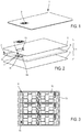
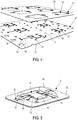
- a smart card 1 comprises a module 2.
- the smart card 1 consists of several layers 3, 4, 5 laminated one on the other.
- the lower finishing layers 3 and upper 5 can be, for example, printed PVC layers.
- the antenna support 4 is generally itself, in a known manner, composed of several layers between which a wired or engraved antenna is integrated in a metal sheet (on the figure 2 , the antenna 6 inserted between two layers is shown in dotted lines).
- the various layers constituting the antenna support 4 are for example also made of PVC.
- the antenna 6 comprises for example a conductive line wound on several loops extending around the periphery of the card 1. Each of the two ends of the line is connected to a connection pad 7.
- the connection pads 7 are at least partly visible and accessible at an opening 8 formed in an upper layer 9 of the antenna support 4.
- the connection pads 7 comprise, for example, solder pads 10.
- the solder pads 10 are made of a material having a melting temperature between 120 ° C and 230 ° C, and more preferably between 160 ° C and 190 ° C.
- the module 2 manufacturing process includes the production of metal contacts 12 on a flexible substrate 13 (see figure 3 ).
- the substrate 13 has a first 14 and a second 15 main faces, with the contacts 12 on the first face 14 of the substrate 13 (front face or contact face).
- connection wells 16 are perforated to produce connection wells 16, the bottom of which is closed by the contacts 12.
- Chips 17 are bonded to the rear face 15 of the substrate 13 (bonding face).
- Each chip 17 is connected using conductive wires 18 connecting, through the connection wells 16, contacts 12 to connection pads of the chip 17.
- connection pads of the chip are connected, also by wires 18 passing through connection wells 16, each respectively to a transfer pad 19.
- Each transfer pad 19 is produced similarly to the contacts 12 and simultaneously with these.
- the wires 18 for connecting the chip 17 to the antenna 6 are therefore each connected by a first end to the chip 17 and by a second end to a transfer pad 19.
- a layer of hot-melt material 20 in which openings 21, 22 are formed is then applied to the rear face 15 of the substrate 13.
- This layer of hot-melt material 20 makes it possible to fix the module 2 in its cavity 11 milled in the card 1.
- the openings 21, 22 are of two types: large openings 21 in which take place the chips 17 and the connection wires 18 from the chip 17 to the contacts 12, and smaller windows 22, through each of which a connection wire 18 from chip 17 to antenna 6 remains visible and accessible.
- Each of these windows 22 is crossed by a portion 23 of the wire 18 for connection of the chip 17 to the antenna 7 (See FIG. 5 ).
- This portion 23 of the wire 18 is held on two opposite sides of each window 22, between the hot-melt material 20 and the substrate 13.
- the portion 23 of the wire 18 passing through each window 22 is relatively free. It extends over the surface of the substrate 13 without adhering to it.
- An encapsulation resin 25 covers the chip 17 and the wires 18 connecting the chip 17 to the contacts 12.
- the drop of encapsulation resin 25 is circumscribed by the edge of the large openings 21.
- the windows 22 through which passes a portion 23 of the wires 18 for connecting the chip 17 to the antenna 6 are devoid of resin 25.
- the module 2 is then transferred to a cavity 11 milled in a smart card 1.
- the windows 23 crossed by the wires 18 for connecting the chip 17 to the antenna 6 are placed opposite the connection pads 7 of the antenna 6 left visible in the cavity 11.
- thermode (not shown) is applied to the contact face 14 of the module 2.
- the heat supplied by the thermode reactivates the hot-melt material 20 situated on the rear face 15 of the module 2.
- the hot-melt material 20 adheres to flanges 24 created in the cavity 11 during milling.
- the thermode melts the solder pads 10 placed on the connection pads 7 of the antenna 6.
- the thermode is for example heated to a temperature between 120 ° C. and 250 ° C.
- the conduction of heat between the thermode and the solder pad 10 is particularly effective since it takes place only through the contacts 12 which are good thermal conductors and the substrate 13.
- the molten solder of the solder pads 10 comes into contact with the portion 23 of wire 18 passing through each window 22.
- the portion 23 of wire 18 thus partially coated with solder is then electrically connected to the antenna 6.
- the solder not adhering to the substrate 13 or to the hot-melt material 20 the portion 23 of wire 18 taken in the weld is integral with the connection pads 7 of the antenna 6, but retains a relative freedom of movement relative to the module 2.
- This relative freedom of movement and the elongation properties of the wire 18 make it possible to compensate for the movements of the module 2 relative to the rest of the body of the card 1, and to absorb the stresses generated between them, when the latter is used , and avoid accidental disconnections from the antenna 6 sometimes observed in the maps of the prior art.
Landscapes
- Engineering & Computer Science (AREA)
- Microelectronics & Electronic Packaging (AREA)
- Computer Hardware Design (AREA)
- Physics & Mathematics (AREA)
- General Physics & Mathematics (AREA)
- Theoretical Computer Science (AREA)
- Condensed Matter Physics & Semiconductors (AREA)
- Power Engineering (AREA)
- Computer Networks & Wireless Communication (AREA)
- Credit Cards Or The Like (AREA)
Applications Claiming Priority (2)
| Application Number | Priority Date | Filing Date | Title |
|---|---|---|---|
| FR1650587A FR3047101B1 (fr) | 2016-01-26 | 2016-01-26 | Procede de fabrication d’un module de carte a puce et d’une carte a puce |
| PCT/FR2017/050172 WO2017129904A1 (fr) | 2016-01-26 | 2017-01-25 | Procédé de fabrication d'un module de carte à puce et d'une carte à puce |
Publications (2)
| Publication Number | Publication Date |
|---|---|
| EP3408799A1 EP3408799A1 (fr) | 2018-12-05 |
| EP3408799B1 true EP3408799B1 (fr) | 2020-07-08 |
Family
ID=56117830
Family Applications (1)
| Application Number | Title | Priority Date | Filing Date |
|---|---|---|---|
| EP17707369.9A Active EP3408799B1 (fr) | 2016-01-26 | 2017-01-25 | Procédé de fabrication d'un module de carte à puce et d'une carte à puce |
Country Status (13)
| Country | Link |
|---|---|
| US (1) | US10706346B2 (ja) |
| EP (1) | EP3408799B1 (ja) |
| JP (1) | JP6901207B2 (ja) |
| CN (1) | CN108496187B (ja) |
| BR (1) | BR112018014282A2 (ja) |
| CL (1) | CL2018002017A1 (ja) |
| ES (1) | ES2817578T3 (ja) |
| FR (1) | FR3047101B1 (ja) |
| MX (1) | MX2018009123A (ja) |
| MY (1) | MY197068A (ja) |
| SG (2) | SG11201806384RA (ja) |
| TW (1) | TWI662480B (ja) |
| WO (1) | WO2017129904A1 (ja) |
Families Citing this family (4)
| Publication number | Priority date | Publication date | Assignee | Title |
|---|---|---|---|---|
| FR3063555B1 (fr) * | 2017-03-03 | 2021-07-09 | Linxens Holding | Carte a puce et procede de fabrication d’une carte a puce |
| WO2019138260A1 (en) * | 2018-01-12 | 2019-07-18 | Linxens Holding | Method for manufacturing a sim card and sim card |
| FR3086098B1 (fr) * | 2018-09-18 | 2020-12-04 | Smart Packaging Solutions | Procede de fabrication d'un module electronique pour objet portatif |
| CN111626395A (zh) * | 2020-05-29 | 2020-09-04 | 东信和平科技股份有限公司 | 一种双界面安全芯片卡及制作方法 |
Citations (13)
| Publication number | Priority date | Publication date | Assignee | Title |
|---|---|---|---|---|
| US4897534A (en) | 1986-11-20 | 1990-01-30 | Gao Gesellschaft Fur Automation Und Organisation Mbh | Data carrier having an integrated circuit and a method for producing the same |
| US5080279A (en) | 1990-06-27 | 1992-01-14 | At&T Bell Laboratories | Method for tape automated bonding |
| JPH08282167A (ja) | 1995-04-13 | 1996-10-29 | Rohm Co Ltd | Icカード |
| US5598032A (en) | 1994-02-14 | 1997-01-28 | Gemplus Card International | Hybrid chip card capable of both contact and contact-free operation and having antenna contacts situated in a cavity for an electronic module |
| JPH10203065A (ja) | 1997-01-27 | 1998-08-04 | Dainippon Printing Co Ltd | Icモジュールの製造方法及びicモジュール |
| US6719206B1 (en) | 1997-11-19 | 2004-04-13 | On Track Innovations Ltd. | Data transaction card and method of manufacture thereof |
| FR2847365A1 (fr) | 2002-11-15 | 2004-05-21 | Gemplus Card Int | Connexion/raccordement simultane par un percage d'adhesif d'encartage |
| US7331528B2 (en) | 2002-12-05 | 2008-02-19 | Muehlbauer Ag | Smartcard and method for production of a smartcard |
| JP2010072930A (ja) | 2008-09-18 | 2010-04-02 | Toshiba Corp | Icモジュール、及びこれを用いたicカード |
| US8172978B2 (en) | 2007-10-11 | 2012-05-08 | Ask S.A. | Reinforced radio frequency identification device support and its manufacturing method |
| US20150269476A1 (en) | 2012-10-15 | 2015-09-24 | Smart Packaging Solutions | Simplified electronic module for a smart card with a dual communication interface |
| FR3021145A1 (fr) | 2014-05-14 | 2015-11-20 | Linxens Holding | Procede de fabrication d'un circuit pour module de carte a puce et circuit pour module de carte a puce |
| EP3059698A1 (fr) | 2015-02-20 | 2016-08-24 | Gemalto Sa | Procédé de fabrication d'un module électronique simple face comprenant des zones d'interconnexion |
Family Cites Families (12)
| Publication number | Priority date | Publication date | Assignee | Title |
|---|---|---|---|---|
| US5671525A (en) * | 1995-02-13 | 1997-09-30 | Gemplus Card International | Method of manufacturing a hybrid chip card |
| US6046504A (en) * | 1997-02-17 | 2000-04-04 | Nippon Steel Corporation | Resin-encapsulated LOC semiconductor device having a thin inner lead |
| JP4471926B2 (ja) * | 2003-05-30 | 2010-06-02 | 株式会社ルネサステクノロジ | 半導体装置 |
| US20070290048A1 (en) * | 2006-06-20 | 2007-12-20 | Innovatier, Inc. | Embedded electronic device and method for manufacturing an embedded electronic device |
| JP6036701B2 (ja) * | 2011-11-17 | 2016-11-30 | 凸版印刷株式会社 | 複合icカード |
| MX2014008936A (es) * | 2012-01-23 | 2015-06-02 | Feinics Amatech Teoranta | Protección de compensacion y acoplamiento mejorado en tarjetas inteligentes metalizadas. |
| CN203134786U (zh) | 2012-12-28 | 2013-08-14 | 日月光封装测试(上海)有限公司 | 半导体封装用导线架条及其模具 |
| DE102013102718A1 (de) * | 2013-03-18 | 2014-09-18 | Infineon Technologies Ag | Chipkartenmodulanordnung |
| JP6090006B2 (ja) * | 2013-06-25 | 2017-03-08 | 凸版印刷株式会社 | Icモジュール、デュアルicカードおよびicモジュールの製造方法 |
| US9424507B2 (en) * | 2014-04-01 | 2016-08-23 | Nxp B.V. | Dual interface IC card components and method for manufacturing the dual-interface IC card components |
| DE102014107299B4 (de) * | 2014-05-23 | 2019-03-28 | Infineon Technologies Ag | Chipkartenmodul, Chipkarte, und Verfahren zum Herstellen eines Chipkartenmoduls |
| TWM544072U (zh) | 2017-04-10 | 2017-06-21 | Tendays Co Ltd | 床組的遠端控制系統 |
-
2016
- 2016-01-26 FR FR1650587A patent/FR3047101B1/fr active Active
-
2017
- 2017-01-25 EP EP17707369.9A patent/EP3408799B1/fr active Active
- 2017-01-25 MX MX2018009123A patent/MX2018009123A/es unknown
- 2017-01-25 BR BR112018014282-4A patent/BR112018014282A2/pt not_active Application Discontinuation
- 2017-01-25 ES ES17707369T patent/ES2817578T3/es active Active
- 2017-01-25 CN CN201780008226.8A patent/CN108496187B/zh active Active
- 2017-01-25 SG SG11201806384RA patent/SG11201806384RA/en unknown
- 2017-01-25 US US16/070,814 patent/US10706346B2/en active Active
- 2017-01-25 MY MYPI2018702609A patent/MY197068A/en unknown
- 2017-01-25 SG SG10201913048XA patent/SG10201913048XA/en unknown
- 2017-01-25 JP JP2018557217A patent/JP6901207B2/ja active Active
- 2017-01-25 WO PCT/FR2017/050172 patent/WO2017129904A1/fr active Application Filing
- 2017-01-26 TW TW106103346A patent/TWI662480B/zh active
-
2018
- 2018-07-25 CL CL2018002017A patent/CL2018002017A1/es unknown
Patent Citations (13)
| Publication number | Priority date | Publication date | Assignee | Title |
|---|---|---|---|---|
| US4897534A (en) | 1986-11-20 | 1990-01-30 | Gao Gesellschaft Fur Automation Und Organisation Mbh | Data carrier having an integrated circuit and a method for producing the same |
| US5080279A (en) | 1990-06-27 | 1992-01-14 | At&T Bell Laboratories | Method for tape automated bonding |
| US5598032A (en) | 1994-02-14 | 1997-01-28 | Gemplus Card International | Hybrid chip card capable of both contact and contact-free operation and having antenna contacts situated in a cavity for an electronic module |
| JPH08282167A (ja) | 1995-04-13 | 1996-10-29 | Rohm Co Ltd | Icカード |
| JPH10203065A (ja) | 1997-01-27 | 1998-08-04 | Dainippon Printing Co Ltd | Icモジュールの製造方法及びicモジュール |
| US6719206B1 (en) | 1997-11-19 | 2004-04-13 | On Track Innovations Ltd. | Data transaction card and method of manufacture thereof |
| FR2847365A1 (fr) | 2002-11-15 | 2004-05-21 | Gemplus Card Int | Connexion/raccordement simultane par un percage d'adhesif d'encartage |
| US7331528B2 (en) | 2002-12-05 | 2008-02-19 | Muehlbauer Ag | Smartcard and method for production of a smartcard |
| US8172978B2 (en) | 2007-10-11 | 2012-05-08 | Ask S.A. | Reinforced radio frequency identification device support and its manufacturing method |
| JP2010072930A (ja) | 2008-09-18 | 2010-04-02 | Toshiba Corp | Icモジュール、及びこれを用いたicカード |
| US20150269476A1 (en) | 2012-10-15 | 2015-09-24 | Smart Packaging Solutions | Simplified electronic module for a smart card with a dual communication interface |
| FR3021145A1 (fr) | 2014-05-14 | 2015-11-20 | Linxens Holding | Procede de fabrication d'un circuit pour module de carte a puce et circuit pour module de carte a puce |
| EP3059698A1 (fr) | 2015-02-20 | 2016-08-24 | Gemalto Sa | Procédé de fabrication d'un module électronique simple face comprenant des zones d'interconnexion |
Non-Patent Citations (2)
| Title |
|---|
| ANONYMOUS: "Ruhlamat", WEBPAGE, 11 October 2015 (2015-10-11), pages 1 - 1 |
| MAUREL F.: "Update on dual interface", NBS TECHNOLOGY INC., February 2013 (2013-02-01), pages 1 - 9, XP055797531 |
Also Published As
| Publication number | Publication date |
|---|---|
| CN108496187A (zh) | 2018-09-04 |
| US20190026621A1 (en) | 2019-01-24 |
| TW201732688A (zh) | 2017-09-16 |
| WO2017129904A1 (fr) | 2017-08-03 |
| JP2019504431A (ja) | 2019-02-14 |
| TWI662480B (zh) | 2019-06-11 |
| JP6901207B2 (ja) | 2021-07-14 |
| CL2018002017A1 (es) | 2019-03-08 |
| ES2817578T3 (es) | 2021-04-07 |
| MY197068A (en) | 2023-05-24 |
| FR3047101A1 (fr) | 2017-07-28 |
| US10706346B2 (en) | 2020-07-07 |
| SG11201806384RA (en) | 2018-08-30 |
| FR3047101B1 (fr) | 2022-04-01 |
| BR112018014282A2 (pt) | 2018-12-18 |
| MX2018009123A (es) | 2018-11-09 |
| SG10201913048XA (en) | 2020-02-27 |
| EP3408799A1 (fr) | 2018-12-05 |
| CN108496187B (zh) | 2021-12-28 |
Similar Documents
| Publication | Publication Date | Title |
|---|---|---|
| EP3143557B1 (fr) | Procédé de fabrication d'un circuit pour module de carte à puce et circuit pour module de carte à puce | |
| EP3201843B1 (fr) | Procédé de fabrication de carte à puce et carte à puce obtenue par ce procédé. | |
| EP3408799B1 (fr) | Procédé de fabrication d'un module de carte à puce et d'une carte à puce | |
| EP3437028B1 (fr) | Procédés de fabrication de cartes à puce et de supports d'antenne pour carte à puce | |
| EP3005846B1 (fr) | Procédé de fabrication d'un circuit imprimé | |
| EP3877909B1 (fr) | Module électronique pour carte à puce | |
| FR2794266A1 (fr) | Procede de fabrication de dispositif electronique portable a circuit integre comportant un dielectrique bas cout | |
| EP2866173B1 (fr) | Procédé de réalisation d'un circuit électrique et circuit électrique réalisé par ce procédé | |
| CA2968070A1 (fr) | Procede de fabrication d'un module electronique simple face comprenant des zones d'interconnexion | |
| EP1192593B1 (fr) | Dispositif et procede de fabrication de dispositifs comprenant au moins une puce montee sur un support | |
| EP4154180B1 (fr) | Procédé de métallisation électro-chimique d'un circuit électrique double-face pour carte à puce et circuit électrique obtenu par ce procédé | |
| WO2017191414A1 (fr) | Procédé de fabrication de cartes à puce et carte à puce obtenue par ce procédé | |
| FR2786009A1 (fr) | Procede de fabrication d'une carte a puce hybride par impression double face | |
| FR2786317A1 (fr) | Procede de fabrication de carte a puce a contact affleurant utilisant une etape de gravure au laser et carte a puce obtenue par le procede | |
| EP2608114A1 (fr) | Procédé de fabrication d'un module à puce de circuit intégré protégé par pastille | |
| EP2825001A1 (fr) | Module électronique à film dielectrique adhésif et son procédé de fabrication | |
| EP3020068B1 (fr) | Module electronique et son procede de fabrication | |
| EP1210690B1 (fr) | Dispositif electronique comportant au moins une puce fixee sur un support et procede de fabrication d'un tel dispositif | |
| WO2001015504A1 (fr) | Procede de fabrication de cartes a puce hybrides et cartes a puce obtenues par ledit procede | |
| FR2790850A1 (fr) | Procede de fabrication de dispositif electronique portable de type carte a puce |
Legal Events
| Date | Code | Title | Description |
|---|---|---|---|
| STAA | Information on the status of an ep patent application or granted ep patent |
Free format text: STATUS: UNKNOWN |
|
| STAA | Information on the status of an ep patent application or granted ep patent |
Free format text: STATUS: THE INTERNATIONAL PUBLICATION HAS BEEN MADE |
|
| PUAI | Public reference made under article 153(3) epc to a published international application that has entered the european phase |
Free format text: ORIGINAL CODE: 0009012 |
|
| STAA | Information on the status of an ep patent application or granted ep patent |
Free format text: STATUS: REQUEST FOR EXAMINATION WAS MADE |
|
| 17P | Request for examination filed |
Effective date: 20180725 |
|
| AK | Designated contracting states |
Kind code of ref document: A1 Designated state(s): AL AT BE BG CH CY CZ DE DK EE ES FI FR GB GR HR HU IE IS IT LI LT LU LV MC MK MT NL NO PL PT RO RS SE SI SK SM TR |
|
| AX | Request for extension of the european patent |
Extension state: BA ME |
|
| DAV | Request for validation of the european patent (deleted) | ||
| DAX | Request for extension of the european patent (deleted) | ||
| STAA | Information on the status of an ep patent application or granted ep patent |
Free format text: STATUS: EXAMINATION IS IN PROGRESS |
|
| 17Q | First examination report despatched |
Effective date: 20190709 |
|
| REG | Reference to a national code |
Ref country code: HK Ref legal event code: DE Ref document number: 1261295 Country of ref document: HK |
|
| GRAP | Despatch of communication of intention to grant a patent |
Free format text: ORIGINAL CODE: EPIDOSNIGR1 |
|
| STAA | Information on the status of an ep patent application or granted ep patent |
Free format text: STATUS: GRANT OF PATENT IS INTENDED |
|
| INTG | Intention to grant announced |
Effective date: 20200129 |
|
| GRAS | Grant fee paid |
Free format text: ORIGINAL CODE: EPIDOSNIGR3 |
|
| GRAA | (expected) grant |
Free format text: ORIGINAL CODE: 0009210 |
|
| STAA | Information on the status of an ep patent application or granted ep patent |
Free format text: STATUS: THE PATENT HAS BEEN GRANTED |
|
| AK | Designated contracting states |
Kind code of ref document: B1 Designated state(s): AL AT BE BG CH CY CZ DE DK EE ES FI FR GB GR HR HU IE IS IT LI LT LU LV MC MK MT NL NO PL PT RO RS SE SI SK SM TR |
|
| REG | Reference to a national code |
Ref country code: AT Ref legal event code: REF Ref document number: 1289257 Country of ref document: AT Kind code of ref document: T Effective date: 20200715 Ref country code: CH Ref legal event code: EP |
|
| REG | Reference to a national code |
Ref country code: DE Ref legal event code: R096 Ref document number: 602017019346 Country of ref document: DE |
|
| REG | Reference to a national code |
Ref country code: IE Ref legal event code: FG4D Free format text: LANGUAGE OF EP DOCUMENT: FRENCH |
|
| REG | Reference to a national code |
Ref country code: NL Ref legal event code: FP |
|
| REG | Reference to a national code |
Ref country code: LT Ref legal event code: MG4D |
|
| PG25 | Lapsed in a contracting state [announced via postgrant information from national office to epo] |
Ref country code: NO Free format text: LAPSE BECAUSE OF FAILURE TO SUBMIT A TRANSLATION OF THE DESCRIPTION OR TO PAY THE FEE WITHIN THE PRESCRIBED TIME-LIMIT Effective date: 20201008 Ref country code: GR Free format text: LAPSE BECAUSE OF FAILURE TO SUBMIT A TRANSLATION OF THE DESCRIPTION OR TO PAY THE FEE WITHIN THE PRESCRIBED TIME-LIMIT Effective date: 20201009 Ref country code: FI Free format text: LAPSE BECAUSE OF FAILURE TO SUBMIT A TRANSLATION OF THE DESCRIPTION OR TO PAY THE FEE WITHIN THE PRESCRIBED TIME-LIMIT Effective date: 20200708 Ref country code: SE Free format text: LAPSE BECAUSE OF FAILURE TO SUBMIT A TRANSLATION OF THE DESCRIPTION OR TO PAY THE FEE WITHIN THE PRESCRIBED TIME-LIMIT Effective date: 20200708 Ref country code: BG Free format text: LAPSE BECAUSE OF FAILURE TO SUBMIT A TRANSLATION OF THE DESCRIPTION OR TO PAY THE FEE WITHIN THE PRESCRIBED TIME-LIMIT Effective date: 20201008 Ref country code: LT Free format text: LAPSE BECAUSE OF FAILURE TO SUBMIT A TRANSLATION OF THE DESCRIPTION OR TO PAY THE FEE WITHIN THE PRESCRIBED TIME-LIMIT Effective date: 20200708 Ref country code: HR Free format text: LAPSE BECAUSE OF FAILURE TO SUBMIT A TRANSLATION OF THE DESCRIPTION OR TO PAY THE FEE WITHIN THE PRESCRIBED TIME-LIMIT Effective date: 20200708 Ref country code: PT Free format text: LAPSE BECAUSE OF FAILURE TO SUBMIT A TRANSLATION OF THE DESCRIPTION OR TO PAY THE FEE WITHIN THE PRESCRIBED TIME-LIMIT Effective date: 20201109 |
|
| PG25 | Lapsed in a contracting state [announced via postgrant information from national office to epo] |
Ref country code: IS Free format text: LAPSE BECAUSE OF FAILURE TO SUBMIT A TRANSLATION OF THE DESCRIPTION OR TO PAY THE FEE WITHIN THE PRESCRIBED TIME-LIMIT Effective date: 20201108 Ref country code: PL Free format text: LAPSE BECAUSE OF FAILURE TO SUBMIT A TRANSLATION OF THE DESCRIPTION OR TO PAY THE FEE WITHIN THE PRESCRIBED TIME-LIMIT Effective date: 20200708 Ref country code: RS Free format text: LAPSE BECAUSE OF FAILURE TO SUBMIT A TRANSLATION OF THE DESCRIPTION OR TO PAY THE FEE WITHIN THE PRESCRIBED TIME-LIMIT Effective date: 20200708 Ref country code: LV Free format text: LAPSE BECAUSE OF FAILURE TO SUBMIT A TRANSLATION OF THE DESCRIPTION OR TO PAY THE FEE WITHIN THE PRESCRIBED TIME-LIMIT Effective date: 20200708 |
|
| REG | Reference to a national code |
Ref country code: DE Ref legal event code: R026 Ref document number: 602017019346 Country of ref document: DE Ref country code: ES Ref legal event code: FG2A Ref document number: 2817578 Country of ref document: ES Kind code of ref document: T3 Effective date: 20210407 |
|
| PLBI | Opposition filed |
Free format text: ORIGINAL CODE: 0009260 |
|
| PLAX | Notice of opposition and request to file observation + time limit sent |
Free format text: ORIGINAL CODE: EPIDOSNOBS2 |
|
| PG25 | Lapsed in a contracting state [announced via postgrant information from national office to epo] |
Ref country code: RO Free format text: LAPSE BECAUSE OF FAILURE TO SUBMIT A TRANSLATION OF THE DESCRIPTION OR TO PAY THE FEE WITHIN THE PRESCRIBED TIME-LIMIT Effective date: 20200708 Ref country code: DK Free format text: LAPSE BECAUSE OF FAILURE TO SUBMIT A TRANSLATION OF THE DESCRIPTION OR TO PAY THE FEE WITHIN THE PRESCRIBED TIME-LIMIT Effective date: 20200708 Ref country code: CZ Free format text: LAPSE BECAUSE OF FAILURE TO SUBMIT A TRANSLATION OF THE DESCRIPTION OR TO PAY THE FEE WITHIN THE PRESCRIBED TIME-LIMIT Effective date: 20200708 Ref country code: SM Free format text: LAPSE BECAUSE OF FAILURE TO SUBMIT A TRANSLATION OF THE DESCRIPTION OR TO PAY THE FEE WITHIN THE PRESCRIBED TIME-LIMIT Effective date: 20200708 Ref country code: EE Free format text: LAPSE BECAUSE OF FAILURE TO SUBMIT A TRANSLATION OF THE DESCRIPTION OR TO PAY THE FEE WITHIN THE PRESCRIBED TIME-LIMIT Effective date: 20200708 |
|
| 26 | Opposition filed |
Opponent name: THALES DIS FRANCE SA Effective date: 20210407 |
|
| REG | Reference to a national code |
Ref country code: AT Ref legal event code: UEP Ref document number: 1289257 Country of ref document: AT Kind code of ref document: T Effective date: 20200708 |
|
| PG25 | Lapsed in a contracting state [announced via postgrant information from national office to epo] |
Ref country code: AL Free format text: LAPSE BECAUSE OF FAILURE TO SUBMIT A TRANSLATION OF THE DESCRIPTION OR TO PAY THE FEE WITHIN THE PRESCRIBED TIME-LIMIT Effective date: 20200708 |
|
| PG25 | Lapsed in a contracting state [announced via postgrant information from national office to epo] |
Ref country code: SK Free format text: LAPSE BECAUSE OF FAILURE TO SUBMIT A TRANSLATION OF THE DESCRIPTION OR TO PAY THE FEE WITHIN THE PRESCRIBED TIME-LIMIT Effective date: 20200708 |
|
| PLAS | Information related to reply of patent proprietor to notice(s) of opposition deleted |
Free format text: ORIGINAL CODE: EPIDOSDOBS3 |
|
| PLBB | Reply of patent proprietor to notice(s) of opposition received |
Free format text: ORIGINAL CODE: EPIDOSNOBS3 |
|
| PLBB | Reply of patent proprietor to notice(s) of opposition received |
Free format text: ORIGINAL CODE: EPIDOSNOBS3 |
|
| PG25 | Lapsed in a contracting state [announced via postgrant information from national office to epo] |
Ref country code: SI Free format text: LAPSE BECAUSE OF FAILURE TO SUBMIT A TRANSLATION OF THE DESCRIPTION OR TO PAY THE FEE WITHIN THE PRESCRIBED TIME-LIMIT Effective date: 20200708 Ref country code: MC Free format text: LAPSE BECAUSE OF FAILURE TO SUBMIT A TRANSLATION OF THE DESCRIPTION OR TO PAY THE FEE WITHIN THE PRESCRIBED TIME-LIMIT Effective date: 20200708 |
|
| REG | Reference to a national code |
Ref country code: CH Ref legal event code: PL |
|
| PG25 | Lapsed in a contracting state [announced via postgrant information from national office to epo] |
Ref country code: LU Free format text: LAPSE BECAUSE OF NON-PAYMENT OF DUE FEES Effective date: 20210125 |
|
| REG | Reference to a national code |
Ref country code: BE Ref legal event code: MM Effective date: 20210131 |
|
| PG25 | Lapsed in a contracting state [announced via postgrant information from national office to epo] |
Ref country code: LI Free format text: LAPSE BECAUSE OF NON-PAYMENT OF DUE FEES Effective date: 20210131 Ref country code: CH Free format text: LAPSE BECAUSE OF NON-PAYMENT OF DUE FEES Effective date: 20210131 |
|
| PG25 | Lapsed in a contracting state [announced via postgrant information from national office to epo] |
Ref country code: IE Free format text: LAPSE BECAUSE OF NON-PAYMENT OF DUE FEES Effective date: 20210125 |
|
| PG25 | Lapsed in a contracting state [announced via postgrant information from national office to epo] |
Ref country code: BE Free format text: LAPSE BECAUSE OF NON-PAYMENT OF DUE FEES Effective date: 20210131 |
|
| APBM | Appeal reference recorded |
Free format text: ORIGINAL CODE: EPIDOSNREFNO |
|
| APBP | Date of receipt of notice of appeal recorded |
Free format text: ORIGINAL CODE: EPIDOSNNOA2O |
|
| APAH | Appeal reference modified |
Free format text: ORIGINAL CODE: EPIDOSCREFNO |
|
| APBQ | Date of receipt of statement of grounds of appeal recorded |
Free format text: ORIGINAL CODE: EPIDOSNNOA3O |
|
| P01 | Opt-out of the competence of the unified patent court (upc) registered |
Effective date: 20230425 |
|
| PG25 | Lapsed in a contracting state [announced via postgrant information from national office to epo] |
Ref country code: CY Free format text: LAPSE BECAUSE OF FAILURE TO SUBMIT A TRANSLATION OF THE DESCRIPTION OR TO PAY THE FEE WITHIN THE PRESCRIBED TIME-LIMIT Effective date: 20200708 |
|
| PG25 | Lapsed in a contracting state [announced via postgrant information from national office to epo] |
Ref country code: HU Free format text: LAPSE BECAUSE OF FAILURE TO SUBMIT A TRANSLATION OF THE DESCRIPTION OR TO PAY THE FEE WITHIN THE PRESCRIBED TIME-LIMIT; INVALID AB INITIO Effective date: 20170125 |
|
| PGFP | Annual fee paid to national office [announced via postgrant information from national office to epo] |
Ref country code: NL Payment date: 20240123 Year of fee payment: 8 |
|
| PGFP | Annual fee paid to national office [announced via postgrant information from national office to epo] |
Ref country code: ES Payment date: 20240216 Year of fee payment: 8 |
|
| PGFP | Annual fee paid to national office [announced via postgrant information from national office to epo] |
Ref country code: AT Payment date: 20240118 Year of fee payment: 8 |
|
| PG25 | Lapsed in a contracting state [announced via postgrant information from national office to epo] |
Ref country code: MK Free format text: LAPSE BECAUSE OF FAILURE TO SUBMIT A TRANSLATION OF THE DESCRIPTION OR TO PAY THE FEE WITHIN THE PRESCRIBED TIME-LIMIT Effective date: 20200708 |
|
| PGFP | Annual fee paid to national office [announced via postgrant information from national office to epo] |
Ref country code: DE Payment date: 20240119 Year of fee payment: 8 Ref country code: GB Payment date: 20240124 Year of fee payment: 8 |
|
| PGFP | Annual fee paid to national office [announced via postgrant information from national office to epo] |
Ref country code: IT Payment date: 20240131 Year of fee payment: 8 Ref country code: FR Payment date: 20240124 Year of fee payment: 8 |
|
| PG25 | Lapsed in a contracting state [announced via postgrant information from national office to epo] |
Ref country code: TR Free format text: LAPSE BECAUSE OF FAILURE TO SUBMIT A TRANSLATION OF THE DESCRIPTION OR TO PAY THE FEE WITHIN THE PRESCRIBED TIME-LIMIT Effective date: 20200708 |
|
| PG25 | Lapsed in a contracting state [announced via postgrant information from national office to epo] |
Ref country code: MT Free format text: LAPSE BECAUSE OF FAILURE TO SUBMIT A TRANSLATION OF THE DESCRIPTION OR TO PAY THE FEE WITHIN THE PRESCRIBED TIME-LIMIT Effective date: 20200708 |