EP3401712B2 - Optisches element und mit diesem optischen element ausgerüsteter artikel - Google Patents
Optisches element und mit diesem optischen element ausgerüsteter artikel Download PDFInfo
- Publication number
- EP3401712B2 EP3401712B2 EP17736029.4A EP17736029A EP3401712B2 EP 3401712 B2 EP3401712 B2 EP 3401712B2 EP 17736029 A EP17736029 A EP 17736029A EP 3401712 B2 EP3401712 B2 EP 3401712B2
- Authority
- EP
- European Patent Office
- Prior art keywords
- concavo
- convex structure
- convexities
- optical element
- units
- Prior art date
- Legal status (The legal status is an assumption and is not a legal conclusion. Google has not performed a legal analysis and makes no representation as to the accuracy of the status listed.)
- Active
Links
Images


Classifications
-
- G—PHYSICS
- G02—OPTICS
- G02B—OPTICAL ELEMENTS, SYSTEMS OR APPARATUS
- G02B5/00—Optical elements other than lenses
- G02B5/18—Diffraction gratings
- G02B5/1847—Manufacturing methods
-
- B—PERFORMING OPERATIONS; TRANSPORTING
- B42—BOOKBINDING; ALBUMS; FILES; SPECIAL PRINTED MATTER
- B42D—BOOKS; BOOK COVERS; LOOSE LEAVES; PRINTED MATTER CHARACTERISED BY IDENTIFICATION OR SECURITY FEATURES; PRINTED MATTER OF SPECIAL FORMAT OR STYLE NOT OTHERWISE PROVIDED FOR; DEVICES FOR USE THEREWITH AND NOT OTHERWISE PROVIDED FOR; MOVABLE-STRIP WRITING OR READING APPARATUS
- B42D25/00—Information-bearing cards or sheet-like structures characterised by identification or security features; Manufacture thereof
- B42D25/20—Information-bearing cards or sheet-like structures characterised by identification or security features; Manufacture thereof characterised by a particular use or purpose
- B42D25/21—Information-bearing cards or sheet-like structures characterised by identification or security features; Manufacture thereof characterised by a particular use or purpose for multiple purposes
-
- B—PERFORMING OPERATIONS; TRANSPORTING
- B42—BOOKBINDING; ALBUMS; FILES; SPECIAL PRINTED MATTER
- B42D—BOOKS; BOOK COVERS; LOOSE LEAVES; PRINTED MATTER CHARACTERISED BY IDENTIFICATION OR SECURITY FEATURES; PRINTED MATTER OF SPECIAL FORMAT OR STYLE NOT OTHERWISE PROVIDED FOR; DEVICES FOR USE THEREWITH AND NOT OTHERWISE PROVIDED FOR; MOVABLE-STRIP WRITING OR READING APPARATUS
- B42D25/00—Information-bearing cards or sheet-like structures characterised by identification or security features; Manufacture thereof
- B42D25/30—Identification or security features, e.g. for preventing forgery
- B42D25/324—Reliefs
-
- B—PERFORMING OPERATIONS; TRANSPORTING
- B42—BOOKBINDING; ALBUMS; FILES; SPECIAL PRINTED MATTER
- B42D—BOOKS; BOOK COVERS; LOOSE LEAVES; PRINTED MATTER CHARACTERISED BY IDENTIFICATION OR SECURITY FEATURES; PRINTED MATTER OF SPECIAL FORMAT OR STYLE NOT OTHERWISE PROVIDED FOR; DEVICES FOR USE THEREWITH AND NOT OTHERWISE PROVIDED FOR; MOVABLE-STRIP WRITING OR READING APPARATUS
- B42D25/00—Information-bearing cards or sheet-like structures characterised by identification or security features; Manufacture thereof
- B42D25/30—Identification or security features, e.g. for preventing forgery
- B42D25/328—Diffraction gratings; Holograms
-
- B—PERFORMING OPERATIONS; TRANSPORTING
- B42—BOOKBINDING; ALBUMS; FILES; SPECIAL PRINTED MATTER
- B42D—BOOKS; BOOK COVERS; LOOSE LEAVES; PRINTED MATTER CHARACTERISED BY IDENTIFICATION OR SECURITY FEATURES; PRINTED MATTER OF SPECIAL FORMAT OR STYLE NOT OTHERWISE PROVIDED FOR; DEVICES FOR USE THEREWITH AND NOT OTHERWISE PROVIDED FOR; MOVABLE-STRIP WRITING OR READING APPARATUS
- B42D25/00—Information-bearing cards or sheet-like structures characterised by identification or security features; Manufacture thereof
- B42D25/30—Identification or security features, e.g. for preventing forgery
- B42D25/351—Translucent or partly translucent parts, e.g. windows
-
- B—PERFORMING OPERATIONS; TRANSPORTING
- B42—BOOKBINDING; ALBUMS; FILES; SPECIAL PRINTED MATTER
- B42D—BOOKS; BOOK COVERS; LOOSE LEAVES; PRINTED MATTER CHARACTERISED BY IDENTIFICATION OR SECURITY FEATURES; PRINTED MATTER OF SPECIAL FORMAT OR STYLE NOT OTHERWISE PROVIDED FOR; DEVICES FOR USE THEREWITH AND NOT OTHERWISE PROVIDED FOR; MOVABLE-STRIP WRITING OR READING APPARATUS
- B42D25/00—Information-bearing cards or sheet-like structures characterised by identification or security features; Manufacture thereof
- B42D25/30—Identification or security features, e.g. for preventing forgery
- B42D25/36—Identification or security features, e.g. for preventing forgery comprising special materials
- B42D25/373—Metallic materials
-
- G—PHYSICS
- G02—OPTICS
- G02B—OPTICAL ELEMENTS, SYSTEMS OR APPARATUS
- G02B5/00—Optical elements other than lenses
- G02B5/18—Diffraction gratings
Definitions
- Valuable papers such as coupons and checks, cards such as credit cards, cash cards, and ID cards, and certificates such as passports and license certificates generally have an optical element adhered thereto to prevent these articles from being counterfeited.
- optical elements have visual effects that are different from those of normal printed matter.
- counterfeit products are also rampant in fields other than the field of valuable papers or certificates, and becoming a social problem. Therefore, anticounterfeit techniques are increasingly applied to articles in a manner and fields similar to those mentioned above.
- optical elements provided with a diffraction grating are known as optical elements having visual effects different from those of normal printed objects.
- PTL 1 diffraction grating
- PTLs 2 to 5 suggest optical elements having optical effects different from those of the diffraction-grated optical elements. Specifically, the optical elements suggested in these documents each display colors with little observation-angle-dependent chromatic change but achieve high chroma level.
- PTL 6 disclosing an optical element according to the preamble of claim 1, relates to a decorative element, in particular in the form of a transfer film, a laminating film or a security thread.
- the decorative element has a microstructure which generates an optical effect in incident light and/or with light passing through.
- the decorative element has several areas in which an optical effect is generated.
- the microstructure in the areas has a periodic arrangement of base elements, the projection of which onto the base plane preferably has an identical shape.
- the base elements preferably follow on from each other periodically isotropically or pseudo-isotropically in the direction of an azimuth angle which thus describes the spatial direction of the sequence in the x/y plane.
- the distance of the element surfaces of the base elements from the base surface here is preferably constant.
- the optical elements displaying colors of high chroma level have a concavo-convex structure for chromatic display in which convexities (or concavities) are not arrayed at regular intervals, to make the observation-angle-dependent chromatic change small. For this reason, attempts have been made to arrange convexities (or concavities) such that the center-to-center distances of adjacent convexities (or concavities) are random. It is, however, very difficult to completely randomize the center-to-center distances of adjacent convexities (or concavities) throughout the concavo-convex structure. For example, computer-based arrangement of convexities causes a problem of increasing the load imposed on the data generation system. Even if adjacent convexities have random center-to-center distances, convexities may be accidentally distributed at regular intervals in isolated spots. Such a distribution of convexities may result in observation-angle-dependent chromatic change.
- the present invention aims to provide an optical element for displaying colors of high chroma level (termed structural color(s) hereinafter), with a structure that reduces data generation load and with little observation-angle-dependent chromatic change.
- An optical element-equipped article of the present invention is characterized in that the article includes the optical element of the present invention and an article that supports the optical element.
- An optical element and an optical element-equipped article of the present invention have a structure that is capable of reducing data generation load, and displays colors with minimal observation-angle-dependent chromatic change and at high chroma level.
- An optical element according to the present invention includes a concavo-convex structure forming layer having a concavo-convex structure on a surface thereof and a light-reflecting layer covering the surface of the concavo-convex structure of the concavo-convex structure forming layer.
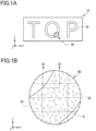
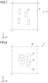
- Fig. 1A is a schematic plan view illustrating an example of an optical element according to the present invention.
- Fig. 1B is an enlarged view of the portion circled by the dash-dot line of Fig. 1A .
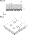
- Fig. 1C is a cross-sectional view taken along the line IC-IC of Fig. 1B .
- the X and Y directions are parallel to the display surface and perpendicular to each other.
- the Z direction is perpendicular to the X and Y directions.
- the optical element according to the present invention includes a unit group UG, where a plurality of units U are arrayed, on a surface of a concavo-convex structure forming layer.
- Each unit U has a concavo-convex structure including a flat portion 21 and convexities 22 (or concavities).
- the concavo-convex structure forming layer may be provided with concavities instead of the convexities 22.
- Convexities or concavities are defined with reference to the surface where they are formed. Recesses formed on the surface serve as concavities, and protrusions formed on the surface serve as the convexities 22.
- the optical element in the example shown in Fig. 1C includes an optically transparent substrate 11, a concavo-convex structure forming layer 12 having a concave structure on the surface on a side opposite to the optically transparent substrate 11, and a light-reflecting layer 13 covering the surface of the concave structure of the concavo-convex structure forming layer 12.
- Components of the optical element will be described below.
- Materials that can be used for the optically transparent substrate 11 include, for example, films or sheets formed of a resin, such as polyethylene terephthalate (PET), polyethylene naphthalate (PEN), polycarbonate (PC), triacetylcellulose (TAC), and acrylic.
- a resin such as polyethylene terephthalate (PET), polyethylene naphthalate (PEN), polycarbonate (PC), triacetylcellulose (TAC), and acrylic.
- PET polyethylene terephthalate
- PEN polyethylene naphthalate
- PC polycarbonate
- TAC triacetylcellulose
- acrylic acrylic
- the optically transparent substrate 11 may be treated according to the purpose of use. Such treatment may be easy adhesion treatment, antifouling treatment, antistatic treatment, anti-abrasion treatment, release treatment, or the like.
- the concavo-convex structure forming layer 12 is typically formed of an optically transparent resin layer.
- the concavo-convex structure forming layer 12 includes a unit group UG made up of a plurality of units U as regions where the concavo-convex structure is defined.
- Each unit U has a specific concavo-convex structure, and this concavo-convex structure includes a flat portion 21 and a plurality of convexities 22 or concavities.
- the concavo-convex structure forming layer 12 may include structure regions different from those of the unit group UG.
- the structures in these regions is not particularly limited as long as the structures are different from that of the unit group UG.
- Examples of the structures in these regions include diffraction grating structures, hologram structures, scattering structures, cross-grating structures, moth-eye structures, various lens structures, and/or flat structures. These structures may each be provided in regions adjacent to or distant from the concavo-convex structure of the unit group UG.
- Materials that can be used for the concavo-convex structure forming layer 12 include, for example, a thermoplastic resin, a thermosetting resin, a radiation-curable resin, and the like.
- thermoplastic resin examples include an acrylic resin, an epoxy resin, a cellulose resin, a vinyl resin, and a mixture of these resins.
- thermosetting resin Materials that can be used for the thermosetting resin include, for example, a urethane resin obtained by crosslinking a polyol resin such as acrylic polyol resin or a polyester polyol resin with an isocyanate compound, a melamine resin, an epoxy resin, a phenolic resin, a mixture of these resins, and the like.
- a polyol resin such as acrylic polyol resin or a polyester polyol resin with an isocyanate compound
- a melamine resin an epoxy resin
- phenolic resin a mixture of these resins, and the like.
- Materials that can be used for the radiation-curable resin include, for example, monomers such as neopentyl glycol acrylate, trimethylolpropane triacrylate, pentaerythritol acrylate, pentaerythritol tetraacrylate, pentaerythritol pentaacrylate, and pentaerythritol hexaacrylate, oligomers such as epoxy acrylate, urethane acrylate, and polyester acrylate, and polymers such as urethane modified acrylic resin, and epoxy-modified acrylic resin, which are radically polymerizable, and include monomers, oligomers, and polymers, which have a cationically polymerizable epoxy group, oxetane skeleton-containing compounds, vinyl ethers, and the like.
- monomers such as neopentyl glycol acrylate, trimethylolpropane triacrylate, pentaerythritol acryl
- various photoinitiators may be combined with the resin.
- the concavo-convex structure forming layer 12 may be made of the same material as that of the optically transparent substrate 11.
- the light-reflecting layer 13 covers a surface of the concavo-convex structure forming layer 12, where the concavo-convex structure is provided.
- the light-reflecting layer 13 may cover the concavo-convex structure forming layer 12 in conformity with the concavo-convex structure thereof, with the thickness being substantially uniform.
- the surface of the light-reflecting layer 13 on a side opposite to the surface contacting the concavo-convex structure forming layer 12 will have a configuration similar to the concavo-convex structure of the concavo-convex structure forming layer 12.
- the light-reflecting layer 13 may be provided such that the surface of the light-reflecting layer 13 on a side opposite to the surface contacting the concavo-convex structure forming layer 12 is flattened. In this case, the thickness of the light-reflecting layer 13 will not be uniform.
- the light-reflecting layer 13 may be a metal layer made of a metallic material such as aluminum, silver, gold, copper, chromium, or an alloy thereof.
- the light-reflecting layer 13 may be a dielectric layer having a refractive index different from that of the concavo-convex structure forming layer 12.
- the light-reflecting layer 13 may be a laminate of dielectric layers, i.e., a dielectric multilayer film, with the refractive index being different between adjacent dielectric layers. If a dielectric multilayer film is used, the refractive index of the dielectric layer contacting the concavo-convex structure forming layer 12 is preferably different from that of the concavo-convex structure forming layer 12.
- An optical element 10 of the present invention may further include other layers such as a release layer, an adhesive layer, a resin layer, and a printed layer.
- the release layer exerts its effects when provided between the optically transparent substrate 11 and the concavo-convex structure forming layer 12, and when the optical element is used as a transfer foil.
- the material for the release layer examples include an acrylic resin, an epoxy resin, a melamine resin, a polyester resin, a polyvinyl chloride-vinyl acetate copolymer resin, a cellulose resin such as triacetylcellulose (TAC), and mixtures thereof.
- acrylic resin an epoxy resin, a melamine resin, a polyester resin, a polyvinyl chloride-vinyl acetate copolymer resin, a cellulose resin such as triacetylcellulose (TAC), and mixtures thereof.
- TAC triacetylcellulose
- the adhesive layer may be provided, for example, covering the light-reflecting layer 13. Provision of the adhesive layer can prevent the surface of the light-reflecting layer 13 from being exposed, making it difficult to duplicate the concavo-convex configuration for counterfeit purposes.
- Examples of the material for the adhesive layer include an acrylic resin, a polyester resin, a polyamide resin, a polyvinyl chloride-vinyl acetate copolymer, an ethylene-vinyl acetate copolymer, an ethylene-acrylic copolymer, chlorinated polypropylene, and mixtures thereof.
- the adhesive layer may contain fillers such as silica, barium sulfate, and talc.
- the resin layer examples include a hard coat layer for preventing scratches on the surface of the optical element 10, an anti-reflecting layer for preventing light from reflecting on the surface of the optically transparent substrate 11, an antistatic layer, and an intermediate layer for improving adhesion between different materials.
- the resin layer can be provided either on the surface of the optically transparent substrate 11 or between any layers of the optical element 10.
- the printed layer is provided to display an image such as of a character, a pattern, or a symbol.
- the printed layer may be provided to the surface of the optically transparent substrate 11 on a side opposite to the surface where the concavo-convex structure forming layer 12 is provided, or may be provided between the concavo-convex structure forming layer 12 and the light-reflecting layer 13, or may be provided on the rear surface of the light-reflecting layer 13.
- inks such as offset ink, letterpress ink, gravure ink, flexographic ink, and screen ink
- inks are used depending on the printing method.
- These inks can be classified into resin-based inks, oil-based inks, water-based inks, etc. according to the compositions, or into oxidative polymerization inks, penetrative drying inks, evaporative drying inks, ultraviolet curable inks, etc. according to the drying methods, and selected as appropriate depending on the type or the printing method of the optically transparent substrate 11.
- a special ink such as a light-emitting (e.g., fluorescent light-emitting) ink, a cholesteric liquid crystal ink, or a pearl ink may be selected as a material for the printed layer.
- the concavo-convex structure of the unit U is the basis of the concavo-convex structure of a unit group.
- matters related to the convexities 22 may be read as matters associated with concavities.
- Fig. 2 is a schematic perspective view illustrating an example of a concavo-convex structure of the unit U of the concavo-convex structure forming layer 12.
- the unit U has a concavo-convex structure that includes the flat portion 21 and the convexities 22.
- each convexity 22 has a square upper surface in plan view; however, the upper surface may have any shape without being limited to such a square shape.
- the upper surface may be in the shape of a triangle, a quadrilateral such as a rectangle or trapezoid, a polygon such as a pentagon or hexagon, a circle, an ellipse, a star, a cross, or an L shape.
- Different shapes may be mixed in the unit U.
- the shapes of the upper surfaces of the convexities 22 may be similar but with different sizes. Furthermore, adjacent convexities 22 may partially overlap.
- the upper surface of the convexity 22 can be in any shape as mentioned above, but, in particular, may preferably be rectangular or square in terms of ease of manufacture.
- convexities 22 there are four convexities 22 in the example shown in Fig. 2 , but any number of convexities 22 may be provided as long as the number is two or more.
- the long sides and the short sides of the upper surfaces of the convexities 22 may have an average length (simply termed average length of the convexities hereinafter), for example, of 0.3 ⁇ m - 10 ⁇ m, more preferably 0.3 ⁇ m - 5 ⁇ m.
- the long side and the short side are defined as follows. Of the line segments connecting between two points on the outline of the upper surface of each convexity 22, the longest one is defined as the long side. Then, a rectangle is drawn circumscribing the outline of the upper surface of the convexity 22 so as to have a side parallel to the long side, and each short side of the rectangle is defined as the short side of the upper surface of the convexity 22. If the upper surface of the convexity 22 has a square shape with sides of equal length and corners of equal internal angle, the long side and the short side should have an equal length.
- the center-to-center distances of adjacent convexities 22 are not constant (i.e., random), and their average is in the range of 1.0 ⁇ m - 3.0 ⁇ m.
- Each center-to-center distance between adjacent convexities 22 refers to the length between the centers or the gravity centers of the upper surfaces of the adjacent convexities 22 concerned.
- each convexity 22 is substantially parallel to the surface of the flat portion 21.
- the upper surface of the convexity 22 and the surface of the flat portion 21 are typically smooth.
- the convexities 22 of the unit U can be arranged as desired as long as adjacent convexities 22 are arranged at random center-to-center distances.
- the following description addresses a non-directional unit in which a plurality of convexities 22 are randomly arranged.
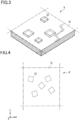
- Fig. 4 is a schematic plan view illustrating an example of a non-directional unit in which a plurality of convexities 22 are randomly arranged.
- each convexity 22 has a square upper surface.
- the sides of the square upper surface have directionality that is not constant between the convexities 22.
- directionality of the sides of the square upper surface is not constant between the convexities 22.
- Fig. 5 is a schematic plan view illustrating another example of a non-directional unit in which a plurality of convexities 22 are randomly arranged.
- each convexity has a rectangular upper surface, and the long sides and the short sides of the surface have directionality that is not constant between the convexities 22.
- each convexity 22 is arranged so that the long sides and the short sides are parallel to the X or Y direction.
- the convexities 22 may be arranged with the long sides and the short sides being oriented in a desired direction.
- the following description addresses a directional unit in which a plurality of convexities 22 are arranged in a specific direction.
- Fig. 6 is a schematic plan view illustrating an example of a directional unit in which a plurality of convexities 22 are arranged in a specific direction.
- each convexity 22 has a square upper surface.
- the sides of the square upper surface have directionality that is constant between the convexities 22.
- the term specific direction refers to an arbitrary direction predetermined in the XY plane.
- directionality of the sides of the square upper surface is constant between the convexities 22.
- Fig. 7 is a schematic plan view illustrating another example of a directional unit in which a plurality of convexities 22 are arranged in a specific direction.
- each convexity 22 has a rectangular upper surface, and the long sides and the short sides of the surface have directionality that is constant between the convexities 22.
- the long sides and the short sides of each convexity 22 are respectively parallel to the Y and X directions.
- the scattering directions of light can be controlled.
- This of arrangement method can change hues of the unit between when observed in the direction of arraying the convexities and when observed in the direction perpendicular to the arrayed direction.
- the unit U may include a concavo-convex structure forming part R1 and a concavo-convex structure non-forming part R2.
- One unit U may include two or more concavo-convex structure forming parts R1.
- the convexities 22 or the concavities of the unit U have a uniform height or depth with reference to the surface of the flat portion.
- the height or depth is in the range of 0.05 ⁇ m - 0.5 ⁇ m, and more preferably 0.07 - 0.4 ⁇ m.
- An excessively small height (or depth) may reduce light interference in a specific wavelength region, and thus the structural color is unlikely to be displayed.
- the light interference herein is in conformity with the height (or depth) defined by the convexities 22 (or concavities) and the flat portion 21.
- external factors during manufacture such as a change in the state and environment of the manufacturing apparatus, and a slight change in the material compositions, may greatly affect the optical properties of the concavo-convex structure.
- An excessively large height of the convexities 22 may cause excessive change in the wavelength of interfering light and may make chromatic change greater, depending on the change in observation angle or direction, and thus the structural color may not be easily recognized.
- the interfering light herein is in conformity with the height (or depth) defined by the convexities 22 (or concavities) and the flat portion 21. It will also be difficult to form the concavo-convex structure with high accuracy in configuration and dimension.
- interference may occur with light of any wavelength in the visible region. If this is the case, light having various wavelengths evenly reaches the observer's eyes, preventing the observer from perceiving particular colors corresponding to the height of the convexities 22 (or depth of the concavities). Accordingly, the observer only perceives the light as being white.
- each convexity 22 (or each concavity) are substantially perpendicular to the upper surface of the convexity 22 (or the bottom surface of the concavity).
- the upper surfaces of the convexities 22 or the bottom surfaces of the concavities have an area occupancy in the range, for example, of 20% - 80%, and more preferably 40% - 60%.
- the area for displaying the structural color is maximized when the ratio of the upper surface area of the convexities 22 or the bottom surface area of the concavities to the flat portion area is 1:1. Therefore, brightest structural color is displayed when the convexities 22 or the concavities have an area occupancy of approximately 50%. With the area occupancy being in the range of 20% - 80%, sufficiently bright display is achieved.
- the unit group UG of the concavo-convex structure forming layer 12 has a concavo-convex structure which is constituted by arraying a plurality of units each having the concavo-convex structure as described above.
- the unit group UG includes units having concavo-convex structures different from each other, and includes units having an identical concavo-convex structure.
- the term units having concavo-convex structures different from each other refers to units each having the convexities 22 arranged differently from other units.
- the term units having an identical concavo-convex structure refers to units having identically arranged convexities 22.
- the optical element having such a concavo-convex structure develops a color (structural color) resulting from interfering light which is attributed to the height that is the surface level difference between the convexities 22 and the flat portion 21, although such an element does not generate diffracted light that would be attributed to a periodic structure.
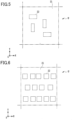
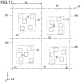
- Fig. 9 is a plan view of an example of a concavo-convex structure of a unit group UG.
- Units U11 - U14 constituting the unit group UG each include the convexities 22 arranged differently from other units.
- the units U11 - U14 all have a square outer shape and are arrayed at a pitch Ud to form the unit group UG.
- the unit pitch Ud herein is in the range of 10 ⁇ m -100 ⁇ m.
- a unit pitch Ud of 10 ⁇ m or more reduces accidental arraying of the convexities at a constant pitch in the concavo-convex structure. Such a range of the unit pitch Ud applies to any of unit arrays described below.
- Fig. 11 is a plan view of an example of a concavo-convex structure of a unit group UG which is made up of an array of units each including a concavo-convex structure forming part R1 and a concavo-convex structure non-forming part R2 shown in Fig. 8 .
- the concavo-convex structure forming part R1 is differently positioned between units U31 to U34.
- the convexities 22 are differently arranged in the concavo-convex structure forming part R1 between the units U31 to U34.
- the convexities 22 are only required to be arranged differently between the units. Accordingly, in the example shown in Fig. 11 , the position of the concavo-convex structure forming part R1 may be the same between the units U31 to U34.
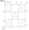
- Fig. 12 is a plan view illustrating an example of a concavo-convex structure of a unit group UG that includes units each constituted only by a concavo-convex structure non-forming part R2 that does not include a concavo-convex structure forming part R1.
- the concavo-convex structure forming part R1 and the concavo-convex structure non-forming part R2 are alternately arrayed as units, but the array is not limited to this.
- the concavo-convex structure forming part R1 and the concavo-convex structure non-forming part R2 may be randomly arranged.
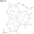
- the unit U which has been described as being rectangular in plan view in the foregoing description, may be hexagonal as shown in Fig. 13 .
- the unit U is in a shape of a square.
- a square is preferable in terms of ease of manufacture.
- the number of units constituting the unit group UG is not limited to the numbers shown in Figs. 9 to 13 , but may be determined as appropriate.
- Fig. 14A is a schematic plan view illustrating an example of a unit group UG in which units having an identical concavo-convex structure are included.
- the unit group UG is made up of square units U11 to U16 each having sides with a length Ud.
- units U11 are arranged in the unit group UG at a 3Ud pitch in the X direction.
- the individual convexities 22 in the units U11 are arrayed at a 3Ud pitch in the X direction.
- Fig. 14A two units 16 are adjacently arrayed as units constituting the unit group UG.
- the units 16 may be taken to be arrayed in the X direction at a 1Ud pitch.
- a unit group includes a plurality of units having an identical concavo-convex structure, it is only when specific units (units 16) are arrayed at a regular interval over a distance of at least 500 ⁇ m, that these units (units 16) are taken to be arrayed at a constant pitch.
- the situation where "in the concavo-convex structure of the unit group UG, units having an identical concavo-convex structure are not arrayed at a pitch of less than 150 ⁇ m" can also be specified using an autocorrelation coefficient.
- the autocorrelation coefficient can be derived from the following autocorrelation function AC(x).
- the concavo-convex cross-section and an arbitrary part thereof can be expressed with functions using a calculated concavo-convex cross-section profile.
- the concavo-convex cross-section profile is calculated based on the information derived from photomicrographs of these concavo-convex cross-sections taken by a scanning electron microscope (SEM), an atomic force microscope (AFM), or the like.
- the autocorrelation coefficient will not be 1 at a pitch of less than 150 ⁇ m.
- the expression "the autocorrelation coefficient will not be 1 at a pitch of less than 150 ⁇ m” includes the case where the autocorrelation coefficient is 1 at a pitch of less than 150 ⁇ m but the size of the array having that pitch is less than 500 ⁇ m. Referring to Figs. 14B and 15 , the autocorrelation coefficient will be more specifically described.
- Fig. 14B is a cross-sectional view taken along the line XIVB-XIVB of Fig. 14A .
- Fig. 14B is a cross-sectional view taken along the line XIVB-XIVB of Fig. 14A .
- the cross-sectional view only the concavo-convex structure forming layer 12 is shown for simplification.
- the line XIVB-XIVB of Fig. 14A for providing the concavo-convex cross-section of Fig. 14B corresponds to the "arbitrary line segment in the plane" in the description of the autocorrelation function set forth above.
- the concavo-convex cross-section shown in Fig. 14B is "the concavo-convex cross-section taken along an arbitrary line segment in the plane”.
- the "an arbitrary part of the concavo-convex cross-section" set forth above is a part arbitrarily selected from the concavo-convex cross-section shown in Fig. 14B .
- an arbitrary part of the concavo-convex cross-section may be the concavo-convex cross-section corresponding to the unit U11 located at the left end of the concavo-convex cross-section shown in Fig. 14B .
- the autocorrelation function AC(x) is yielded by integrating a product of functions P(x') and P(x'+x), over the range of - ⁇ to ⁇ , the latter function being p(x') shifted by x.
- the integral interval which is taken to be in the range of - ⁇ to ⁇ in Formula (1), substantially corresponds to the size (length) of the concavo-convex cross-section in the cutting direction along the arbitrary line segment.
- Fig. 15 is a schematic diagram illustrating a state where the leftmost unit U11 has been moved, relative to the concavo-convex cross-section shown in Fig. 14B .
- x varies from 0 to 9Ud.
- the two functions P(x') and p(x') agree with each other.
- the two functions P(x') and p(x') agree with each other and the autocorrelation coefficient takes a value of 1 at a 3Ud pitch.
- the pitch 3Ud of the autocorrelation coefficient should be not less than 150 ⁇ m, or, although the pitch 3Ud of the autocorrelation coefficient is less than 150 ⁇ m, the size (length 10Ud from the leftmost unit 11 to the rightmost unit 11) of the array having that pitch should be less than 500 ⁇ m.
- an arbitrary part of the concavo-convex cross-section is taken to be the concavo-convex cross-section part of the unit U11, which is the leftmost unit of Fig. 14B .
- an arbitrary part of the concavo-convex cross-section is preferably “an arbitrarily selected 150- ⁇ m length of the concavo-convex cross-section taken along an arbitrary line segment in a plane”.
- an arbitrary part of the concavo-convex cross-section even more preferably has "a length that is ten times the length of an average length of arbitrarily selected convexities or concavities of the concavo-convex cross-section taken along an arbitrary line segment in the plane".
- An excessively small average length of the convexities 22 entails difficulty in determining the pitch that yields the autocorrelation coefficient value of 1.
- the number of units having different concavo-convex structures constituting the unit group UG is not particularly limited, but may preferably be three or more, more preferably five or more, and even more preferably ten or more. Because in a unit group UG identical concavo-convex structure are included, the number of processes for producing units can be reduced.
- use of a dithering method or other randomizing methods can provide an arrangement that satisfies the conditions mentioned above.
- units having an identical concavo-convex structure are preferably not consecutively arrayed over a 0.5-mm or more distance. This is because an array of units having an identical concavo-convex structure over a 0.5-mm or more distance tends to cause diffracted light attributed to the unit pitch, regardless of the unit size.
- the region other than the pattern forming parts 20 typically has a flat structure. Instead, however, such a region may be provided in parallel with various structures such as a diffraction grating structure, a hologram structure, a cross-grating structure, and a lens structure, as stated above.
- the concavo-convex structure may be formed by providing a different unit group UG, for each section of a character or design to be displayed.
- a unit group UG including the convexities 22 (or concavities) with a height (depth) that is different from other sections may be provided, for each section of a character or design to be displayed.
- a plurality of units U having different uneven-structure directivities may be combined with each other.
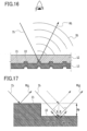
- Fig. 17 is a schematic diagram illustrating how illumination light enters from an optically transparent substrate 11 side into a concavo-convex structure of the concavo-convex structure forming layer 12 and is reflected on the upper surface of the concavity 22 and the flat portion 21 in the optical element 10.
- phase difference between the light RL1 and the light RL2 will be the optical path difference multiplied by 2 ⁇ / ⁇ . Accordingly, the phase difference will be 4 ⁇ ndpcos ⁇ / ⁇ .
- phase difference is an integer multiple of 2 ⁇ , the light RL1 and light RL2 create constructive interference. If the phase difference is equal to a sum of ⁇ and 2 ⁇ that is multiplied by an integer, the light RL1 and light RL2 create destructive interference.
- the convexity height or the concavity depth is constant as in the unit group UG of the present invention, diffraction efficiency is sufficiently small in part of region of the visible wavelength range compared to the rest of the region.
- the observer perceives specific a structural color according to the convexity height or concavity depth when illumination light is applied to the concavo-convex structure of the optical element of the present invention.
- a constant height (or depth) may be applied to the concavities 22 (concavities) of all the characters T, O and P.
- all the characters can be displayed with a single structural color.
- the height (or depth) of the concavities 22 (concavities) may be made different between the characters T, O and P. In this case, these characters are displayed with different structural colors.
- each character may have convexities (concavities) part of which has a height (depth) that is different from the rest of the character. In this case, even more diverse colors can be displayed.
- the optical element of the present invention has a structure that is capable of reducing data generation load, and displays colors having little observation-angle-dependent chromatic change and at high chroma level.
- a metal stamper is prepared through photolithography as follows.
- Electroforming is a kind of surface treatment for forming a metal film on an object by immersing the object in a given aqueous solution and using the reducing power of electrons by energizing the object.
- a method enables precise duplication of a fine concavo-convex structure provided on a surface of the original plate.
- the surface of the object to be electroformed needs to be electrically conductive.
- a thin metal film is provided in advance on a surface of the structural body by vapor phase deposition, such as sputtering or vacuum deposition, prior to electroforming.
- a concavo-convex structure is duplicated.
- a thermoplastic resin or a photocurable resin is applied to an optically transparent substrate 11 which is made of polycarbonate, polyester, or the like.
- the metal stamper is brought into close contact with the coating film, followed by application of heat and pressure or irradiation of light.
- the metal stamper is removed from the resin layer to produce a concavo-convex structure forming layer 12 having a concavo-convex structure.
- a metal such as aluminum, or a dielectric material is deposited on the concavo-convex structure forming layer 12 by vapor deposition, for example, for formation into a single layer or a multilayer, thereby forming a light-reflecting layer 13.
- a metal such as aluminum, or a dielectric material
- the concavo-convex structure forming layer 12 is to be covered with the light-reflecting layer 13
- the light-reflecting layer 13 is formed as a continuous film by vapor-phase deposition, and then part thereof is removed such as by a chemical.
- the optical element 10 is fabricated with the method as described above.
- optical element 10 of the present invention can be used as an anticounterfeit label or the like by being supported by a printed matter or other articles.
- optical elements can provide visual effects, at relatively low cost, which have not been achieved by conventional art, so that they can exert higher anticounterfeit effects for a wide variety of articles.
- Fig. 18 is a schematic plan view illustrating an example of an article with the optical element of the present invention.
- the optical element 10 may be secured to a base material of the article 40 with an adhesive.
- the optical element 10 may be prepared in advance as an adhesive sticker, a transfer foil, or a hologram sheet, and affixed to a base material.
- the transfer foil may be in a stripe or patch shape, and may be applied to the overall surface or part of the surface of the article 40.
- the optical element 10 may be secured to the printed layer of the base material.
- the optical element-equipped article 50 can make the optical effects of the optical element 10 more prominent, when the optical effects of the former are compared with those of the optical element 10 provided to the printed layer.
- the paper may be made with an addition of the optical element 10 thereto while an opening is formed at the position corresponding to the location of the optical element.
- the optical element 10 may be embedded in the article 40. In this case, the optical element 10 can serve as a thread.
- the optical element 10 may be used for purposes other than counterfeit prevention.
- the optical element 10 may be used for toys, learning materials, and accessories. Examples
- the optical element of the present invention was fabricated as follows.
- an ultraviolet curing resin was applied to a polyethylene terephthalate film (termed PET film hereinafter) having a thickness of 80 ⁇ m so that the applied resin will have a uniform thickness.
- this coating film was irradiated with ultraviolet light from a PET film side while a nickel stamper provided with a predetermined concavo-convex structure was pressed against the coating film, thereby curing the ultraviolet curing resin.
- the concavo-convex structure forming layer produced as described above included a unit group where six units A to F were arrayed in the order of ABCDEFADBECFDCABEFDAFDBECBAFCE as a region for a concavo-convex structure provided on one surface thereof.
- the units A to F each had a square outer shape of 30 ⁇ m on each side, and had 230 convexities each having a square upper surface of 1 ⁇ m on each side.
- the upper surfaces of the convexities had an area occupancy of 25.6% in each of the units A to F.
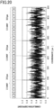
- An autocorrelation coefficient was calculated as follows, for the concavo-convex structure provided to the unit group of the concavo-convex structure forming layer. More specifically, a profile of the concavo-convex cross-section was calculated from a micrograph (e.g., SEM) of a cross-section of the element.
- a micrograph e.g., SEM
- Autocorrelation coefficients calculated in this way are shown in Fig. 20 .
- the autocorrelation coefficient takes a value of 1 at positions 0 ⁇ m, 180 ⁇ m, 420 ⁇ m, 570 ⁇ m, and 780 ⁇ m. It will be understood from this that the autocorrelation coefficient does not take a value of 1 at the pitch of less than 150 ⁇ m.
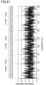
- An optical element was fabricated in a manner similar to Example 1 in the concavo-convex structure forming layer formed in Example 1, except that a unit group made up of six units A to F arrayed in the order of ABCDEFADBEABCDEFADBEABCDEFADBE was used as a unit group included in the region of the concavo-convex structure.
- the autocorrelation coefficients calculated for the concavo-convex structure of the unit group are shown in Fig. 21 .
- the autocorrelation coefficient takes a value of 1 at positions 0 ⁇ m, 180 ⁇ m, 300 ⁇ m, 480 ⁇ m, 600 ⁇ m, and 780 ⁇ m. It will be understood from this that the autocorrelation coefficient does not take a value of 1 at the pitch of less than 150 ⁇ m.
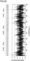
- An optical element was fabricated in a manner similar to Example 1 in the concavo-convex structure forming layer formed in Example 1, except that a unit group made up of six units A to F arrayed in the order of AACFDEBBEDEFCDEBFDBACFACCEFABE was used as a unit group included in the region of the concavo-convex structure.
- the autocorrelation coefficients calculated for the concavo-convex structure of the unit group are shown in Fig. 22 .
- the autocorrelation coefficient takes a value of 1 at positions 0 ⁇ m, 30 ⁇ m, 570 ⁇ m, 660 ⁇ m, and 810 ⁇ m. It will be understood from this that the autocorrelation coefficient does not take a value of 1 at the pitch of less than 150 ⁇ m.
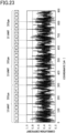
- An optical element was fabricated in a manner similar to Example 1 in the concavo-convex structure forming layer formed in Example 1, except that a unit group made up of six units A to F arrayed in the order of ACAEBADAFCAEABFADAEBAFACDABAED was used as a unit group included in the region of the concavo-convex structure.
- the autocorrelation coefficients calculated for the concavo-convex structure of the unit group are shown in Fig. 23 .
- the autocorrelation coefficient takes a value of 1 at positions 0 ⁇ m, 60 ⁇ m, 150 ⁇ m, 210 ⁇ m, 300 ⁇ m, 360 ⁇ m, 450 ⁇ m, 510 ⁇ m, 600 ⁇ m, 660 ⁇ m, 750 ⁇ m, and 810 ⁇ m.
- the autocorrelation coefficient takes a value of 1 at the pitch of 150 ⁇ m. Since the pitch is not less than 150 ⁇ m, it will be understood that there is no occurrence of a state where the autocorrelation coefficient takes a value of 1 at the pitch of less than 150 ⁇ m.
- An optical element was fabricated in a manner similar to Example 1 in the concavo-convex structure forming layer formed in Example 1, except that the unit group made up of six units A to F arrayed in the order of ABCADEAFEADBADFAFEACBACDAEFABC was used as a unit group of the region for the concavo-convex structure.
- the autocorrelation coefficients calculated for the concavo-convex structure of the unit group are shown in Fig. 24 .
- the autocorrelation coefficient takes a value of 1 at positions 0 ⁇ m, 90 ⁇ m, 180 ⁇ m, 270 ⁇ m, 360 ⁇ m, 450 ⁇ m, 540 ⁇ m, 630 ⁇ m, 720 ⁇ m, and 810 ⁇ m.
- the autocorrelation coefficient takes a value of 1 at the pitch of 90 ⁇ m. It will be understood from this that the autocorrelation coefficient for the concavo-convex structure of the unit group takes a value of 1 at the pitch of less than 150 ⁇ m.
- optical elements fabricated as described above were visually observed under fluorescent light and LED light to confirm the visual effects.
Landscapes
- Physics & Mathematics (AREA)
- General Physics & Mathematics (AREA)
- Optics & Photonics (AREA)
- Engineering & Computer Science (AREA)
- Manufacturing & Machinery (AREA)
- Diffracting Gratings Or Hologram Optical Elements (AREA)
- Optical Elements Other Than Lenses (AREA)
- Credit Cards Or The Like (AREA)
Claims (4)
- Optisches Element (10), umfassend:eine konkav-konvexe strukturbildende Schicht (12), die eine konkav-konvexe Struktur an einer Oberfläche aufweist; undeine lichtreflektierende Schicht (13), die die Oberfläche der konkav-konvexen Struktur der konkav-konvexen strukturbildenden Schicht abdeckt, wobei:die konkav-konvexe strukturbildende Schicht (12) eine Einheitengruppe (UG) umfasst, die eine Vielzahl von Einheiten (U) beinhaltet, deren konkav-konvexe Strukturen sich voneinander unterscheiden und die Einheiten beinhaltet, die eine identische konkav-konvexe Struktur aufweisen;jede der Einheiten einen flachen Abschnitt (21) und entweder eine Vielzahl von Konvexitäten (22) oder eine Vielzahl von Konkavitäten aufweist, mit einer oberen Oberfläche von jeder Konvexität oder einer Bodenfläche von jeder Konkavität im Wesentlichen parallel zur einer Oberfläche des flachen Abschnitts; dadurch gekennzeichnet, dassdie Konvexitäten oder die Konkavitäten, die aneinander angrenzen, Mitte-zu-Mitte-Abstände aufweisen, die nicht regelmäßig sind;die Konvexitäten oder die Konkavitäten eine regelmäßige Höhe oder Tiefe aufweisen;in der Einheitengruppe Einheiten, die eine identische konkav-konvexe Struktur aufweisen, nicht bei einer Teilung von weniger als 150 µm angeordnet sind,konkav-konvexe Strukturen sich zwischen angrenzenden Einheiten unterscheiden;die Einheitengruppe aus direktionalen Einheiten besteht, die die Vielzahl von Konvexitäten oder die Vielzahl von Konkavitäten in einer spezifischen Richtung angeordnet aufweisen;eine Höhe der Konvexitäten oder eine Tiefe der Konkavitäten in einem Bereich von 0,05 µm bis 0,5 µm ist;die angrenzenden Konvexitäten oder die angrenzenden Konkavitäten Mitte-zu-Mitte-Abstände aufweisen, deren Durchschnitt in einem Bereich von 1,0 µm bis 3,0 µm ist;die Einheiten ein Array bilden; unddie Einheiten eine quadratische Außenform aufweisen und bei einer Teilung von 10 µm - 100 µm angeordnet sind, um die Einheitengruppe zu bilden.
- Optisches Element nach Anspruch 1, dadurch gekennzeichnet, dass:wenn in einem konkav-konvexen Querschnitt entlang eines willkürlichen Liniensegments in einer Ebene der konkav-konvexen Struktur der Einheitengruppe der konkav-konvexe Querschnitt und eine willkürlich ausgewählte 150-µm Länge des konkav-konvexen Querschnitts jeweils durch Funktionen P(x') und p(x') angegeben sind, eine Autokorrelationsfunktion AC(x) durch die folgende Formel (1) ausgedrückt werden kann:
 (wo x ein Abstand zwischen den Funktionen P(x') und p(x') in einer Schnittrichtung entlang eines willkürlichen Liniensegments ist); undein Autokorrelationskoeffizient, der von der Autokorrelationsfunktion AC(x) durch die folgende Formel (2) abgeleitet ist, nicht einen Wert von 1 bei einer Teilung von weniger als 150 µm einnimmt:
- Optisches Element nach Anspruch 1, dadurch gekennzeichnet, dass:wenn in einem konkav-konvexen Querschnitt entlang eines willkürlichen Liniensegments in einer Ebene einer konkav-konvexen Struktur der Einheitengruppe der konkav-konvexe Querschnitt und eine Länge, die zehnmal die Länge einer Durchschnittslänge von Konvexitäten oder Konkavitäten des konkav-konvexen Querschnitts ist, jeweils durch Funktionen P(x') und p(x') angegeben sind, eine Autokorrelationsfunktion AC(x) durch die folgende Formel (1) ausgedrückt ist:
 (wo x ein Abstand zwischen den Funktionen P(x') und p(x') in einer Schnittrichtung entlang eines willkürlichen Liniensegments ist); undein Autokorrelationskoeffizient, der von der Autokorrelationsfunktion AC(x) durch die folgende Formel (2) abgeleitet ist, nicht einen Wert von 1 bei einer Teilung von weniger als 150 µm einnimmt:
- Mit optischem Element ausgerüsteter Artikel, dadurch gekennzeichnet, dass der Artikel das optische Element nach einem der Ansprüche 1 bis 3 und einen Artikel, der das optische Element stützt, beinhaltet.
Applications Claiming Priority (2)
| Application Number | Priority Date | Filing Date | Title |
|---|---|---|---|
| JP2016001760 | 2016-01-07 | ||
| PCT/JP2017/000300 WO2017119492A1 (ja) | 2016-01-07 | 2017-01-06 | 光学素子、および光学素子付き物品 |
Publications (4)
| Publication Number | Publication Date |
|---|---|
| EP3401712A1 EP3401712A1 (de) | 2018-11-14 |
| EP3401712A4 EP3401712A4 (de) | 2019-01-23 |
| EP3401712B1 EP3401712B1 (de) | 2020-02-26 |
| EP3401712B2 true EP3401712B2 (de) | 2025-02-26 |
Family
ID=59273649
Family Applications (1)
| Application Number | Title | Priority Date | Filing Date |
|---|---|---|---|
| EP17736029.4A Active EP3401712B2 (de) | 2016-01-07 | 2017-01-06 | Optisches element und mit diesem optischen element ausgerüsteter artikel |
Country Status (4)
| Country | Link |
|---|---|
| US (1) | US10921500B2 (de) |
| EP (1) | EP3401712B2 (de) |
| JP (1) | JP6907943B2 (de) |
| WO (1) | WO2017119492A1 (de) |
Families Citing this family (3)
| Publication number | Priority date | Publication date | Assignee | Title |
|---|---|---|---|---|
| JP6766860B2 (ja) * | 2018-12-06 | 2020-10-14 | 凸版印刷株式会社 | 表示体及び表示体の製造方法 |
| DE102021002599A1 (de) | 2021-05-18 | 2022-11-24 | Giesecke+Devrient Currency Technology Gmbh | Optisch variables Darstellungselement |
| DE102024109646A1 (de) | 2024-04-05 | 2025-10-09 | Giesecke+Devrient Currency Technology Gmbh | Optisch variables Darstellungselement |
Citations (6)
| Publication number | Priority date | Publication date | Assignee | Title |
|---|---|---|---|---|
| EP2077459A1 (de) † | 2006-10-24 | 2009-07-08 | Toppan Printing Co., Ltd. | Anzeigeelement und etikettierter artikel |
| EP2447743A1 (de) † | 2010-11-01 | 2012-05-02 | CSEM Centre Suisse d'Electronique et de Microtechnique SA - Recherche et Développement | Isotropes optisches Filter und Herstellungsverfahren dafür |
| DE102012105571A1 (de) † | 2012-06-26 | 2014-01-02 | Ovd Kinegram Ag | Dekorelement, Sicherheitsdokument mit einem Dekorelement sowie Verfahren zur Herstellung eines Dekorelements |
| WO2014023415A1 (de) † | 2012-08-10 | 2014-02-13 | Giesecke & Devrient Gmbh | Sicherheitselement mit farbeffekterzeugender struktur |
| EP2960690A1 (de) † | 2013-02-21 | 2015-12-30 | Toppan Printing Co., Ltd. | Anzeige und artikel mit einem etikett |
| EP3367140A1 (de) † | 2015-10-19 | 2018-08-29 | Toppan Printing Co., Ltd. | Anzeigekörper, artikel mit anzeigekörper und anzeigekörperbeobachtungsverfahren |
Family Cites Families (10)
| Publication number | Priority date | Publication date | Assignee | Title |
|---|---|---|---|---|
| JPS5143855B2 (de) | 1973-06-07 | 1976-11-25 | ||
| JP2630047B2 (ja) | 1990-09-28 | 1997-07-16 | 凸版印刷株式会社 | 回折格子パターンを有するディスプレイおよびその作製方法 |
| JP2006133625A (ja) * | 2004-11-09 | 2006-05-25 | Nec Lcd Technologies Ltd | 反射板及び該反射板を備える液晶表示装置 |
| EP1855127A1 (de) | 2006-05-12 | 2007-11-14 | Rolic AG | Optisch wirksame Oberflächenreliefmikrostrukturen und Verfahren zu ihrer Herstellung |
| WO2009040960A1 (ja) * | 2007-09-28 | 2009-04-02 | Toppan Printing Co., Ltd. | 表示体及びラベル付き物品 |
| JP5434144B2 (ja) * | 2009-03-03 | 2014-03-05 | 凸版印刷株式会社 | 表示体及びラベル付き物品 |
| JP4983948B2 (ja) | 2010-03-29 | 2012-07-25 | 凸版印刷株式会社 | 表示体及び表示体付き物品 |
| JP4983899B2 (ja) | 2009-12-01 | 2012-07-25 | 凸版印刷株式会社 | 表示体及びラベル付き物品 |
| CN102770787B (zh) * | 2009-12-01 | 2015-09-16 | 凸版印刷株式会社 | 显示体及带标签的物品 |
| JP5143855B2 (ja) * | 2010-04-08 | 2013-02-13 | 凸版印刷株式会社 | 表示体及びラベル付き物品 |
-
2017
- 2017-01-06 WO PCT/JP2017/000300 patent/WO2017119492A1/ja not_active Ceased
- 2017-01-06 EP EP17736029.4A patent/EP3401712B2/de active Active
- 2017-01-06 JP JP2017560436A patent/JP6907943B2/ja active Active
-
2018
- 2018-06-26 US US16/018,275 patent/US10921500B2/en active Active
Patent Citations (6)
| Publication number | Priority date | Publication date | Assignee | Title |
|---|---|---|---|---|
| EP2077459A1 (de) † | 2006-10-24 | 2009-07-08 | Toppan Printing Co., Ltd. | Anzeigeelement und etikettierter artikel |
| EP2447743A1 (de) † | 2010-11-01 | 2012-05-02 | CSEM Centre Suisse d'Electronique et de Microtechnique SA - Recherche et Développement | Isotropes optisches Filter und Herstellungsverfahren dafür |
| DE102012105571A1 (de) † | 2012-06-26 | 2014-01-02 | Ovd Kinegram Ag | Dekorelement, Sicherheitsdokument mit einem Dekorelement sowie Verfahren zur Herstellung eines Dekorelements |
| WO2014023415A1 (de) † | 2012-08-10 | 2014-02-13 | Giesecke & Devrient Gmbh | Sicherheitselement mit farbeffekterzeugender struktur |
| EP2960690A1 (de) † | 2013-02-21 | 2015-12-30 | Toppan Printing Co., Ltd. | Anzeige und artikel mit einem etikett |
| EP3367140A1 (de) † | 2015-10-19 | 2018-08-29 | Toppan Printing Co., Ltd. | Anzeigekörper, artikel mit anzeigekörper und anzeigekörperbeobachtungsverfahren |
Also Published As
| Publication number | Publication date |
|---|---|
| WO2017119492A1 (ja) | 2017-07-13 |
| JP6907943B2 (ja) | 2021-07-21 |
| US20180299596A1 (en) | 2018-10-18 |
| JPWO2017119492A1 (ja) | 2018-11-01 |
| US10921500B2 (en) | 2021-02-16 |
| EP3401712A1 (de) | 2018-11-14 |
| EP3401712B1 (de) | 2020-02-26 |
| EP3401712A4 (de) | 2019-01-23 |
Similar Documents
| Publication | Publication Date | Title |
|---|---|---|
| US10322602B2 (en) | Display and labeled article | |
| CA2686460C (en) | Display and information-printed matter | |
| JP6237759B2 (ja) | 表示体およびラベル付き物品 | |
| JP5938963B2 (ja) | 表示体及びラベル付き物品 | |
| JP5143855B2 (ja) | 表示体及びラベル付き物品 | |
| JP6089387B2 (ja) | 表示体及びラベル付き物品 | |
| US11427025B2 (en) | Display, article with display, and method of observing display | |
| CN107111022A (zh) | 显示体及物品 | |
| JP5741125B2 (ja) | 表示体及びラベル付き物品 | |
| JP2012123102A (ja) | 表示体及びラベル付き物品 | |
| JP2012078447A (ja) | 表示体及びラベル付き物品 | |
| JP2014052527A (ja) | 表示体及び表示体付き物品とその真偽判定方法 | |
| US10921500B2 (en) | Optical element, and optical element-equipped article | |
| JP5407511B2 (ja) | 表示体及び情報印刷物 | |
| JP2016212439A (ja) | 表示体及びラベル付き物品 | |
| JP2016173596A (ja) | 表示体及びラベル付き物品 | |
| JP5994899B2 (ja) | 表示体及びラベル付き物品 | |
| JP2016218093A (ja) | 表示体 |
Legal Events
| Date | Code | Title | Description |
|---|---|---|---|
| STAA | Information on the status of an ep patent application or granted ep patent |
Free format text: STATUS: THE INTERNATIONAL PUBLICATION HAS BEEN MADE |
|
| PUAI | Public reference made under article 153(3) epc to a published international application that has entered the european phase |
Free format text: ORIGINAL CODE: 0009012 |
|
| STAA | Information on the status of an ep patent application or granted ep patent |
Free format text: STATUS: REQUEST FOR EXAMINATION WAS MADE |
|
| 17P | Request for examination filed |
Effective date: 20180704 |
|
| AK | Designated contracting states |
Kind code of ref document: A1 Designated state(s): AL AT BE BG CH CY CZ DE DK EE ES FI FR GB GR HR HU IE IS IT LI LT LU LV MC MK MT NL NO PL PT RO RS SE SI SK SM TR |
|
| AX | Request for extension of the european patent |
Extension state: BA ME |
|
| A4 | Supplementary search report drawn up and despatched |
Effective date: 20181220 |
|
| RIC1 | Information provided on ipc code assigned before grant |
Ipc: G02B 5/18 20060101AFI20181214BHEP Ipc: B42D 25/324 20140101ALI20181214BHEP Ipc: B42D 25/328 20140101ALI20181214BHEP |
|
| DAV | Request for validation of the european patent (deleted) | ||
| DAX | Request for extension of the european patent (deleted) | ||
| GRAP | Despatch of communication of intention to grant a patent |
Free format text: ORIGINAL CODE: EPIDOSNIGR1 |
|
| STAA | Information on the status of an ep patent application or granted ep patent |
Free format text: STATUS: GRANT OF PATENT IS INTENDED |
|
| INTG | Intention to grant announced |
Effective date: 20190904 |
|
| GRAS | Grant fee paid |
Free format text: ORIGINAL CODE: EPIDOSNIGR3 |
|
| GRAA | (expected) grant |
Free format text: ORIGINAL CODE: 0009210 |
|
| STAA | Information on the status of an ep patent application or granted ep patent |
Free format text: STATUS: THE PATENT HAS BEEN GRANTED |
|
| AK | Designated contracting states |
Kind code of ref document: B1 Designated state(s): AL AT BE BG CH CY CZ DE DK EE ES FI FR GB GR HR HU IE IS IT LI LT LU LV MC MK MT NL NO PL PT RO RS SE SI SK SM TR |
|
| REG | Reference to a national code |
Ref country code: GB Ref legal event code: FG4D |
|
| REG | Reference to a national code |
Ref country code: CH Ref legal event code: EP |
|
| REG | Reference to a national code |
Ref country code: AT Ref legal event code: REF Ref document number: 1238340 Country of ref document: AT Kind code of ref document: T Effective date: 20200315 |
|
| REG | Reference to a national code |
Ref country code: IE Ref legal event code: FG4D |
|
| REG | Reference to a national code |
Ref country code: DE Ref legal event code: R096 Ref document number: 602017012350 Country of ref document: DE |
|
| PG25 | Lapsed in a contracting state [announced via postgrant information from national office to epo] |
Ref country code: FI Free format text: LAPSE BECAUSE OF FAILURE TO SUBMIT A TRANSLATION OF THE DESCRIPTION OR TO PAY THE FEE WITHIN THE PRESCRIBED TIME-LIMIT Effective date: 20200226 Ref country code: NO Free format text: LAPSE BECAUSE OF FAILURE TO SUBMIT A TRANSLATION OF THE DESCRIPTION OR TO PAY THE FEE WITHIN THE PRESCRIBED TIME-LIMIT Effective date: 20200526 Ref country code: RS Free format text: LAPSE BECAUSE OF FAILURE TO SUBMIT A TRANSLATION OF THE DESCRIPTION OR TO PAY THE FEE WITHIN THE PRESCRIBED TIME-LIMIT Effective date: 20200226 |
|
| REG | Reference to a national code |
Ref country code: NL Ref legal event code: MP Effective date: 20200226 |
|
| REG | Reference to a national code |
Ref country code: LT Ref legal event code: MG4D |
|
| PG25 | Lapsed in a contracting state [announced via postgrant information from national office to epo] |
Ref country code: GR Free format text: LAPSE BECAUSE OF FAILURE TO SUBMIT A TRANSLATION OF THE DESCRIPTION OR TO PAY THE FEE WITHIN THE PRESCRIBED TIME-LIMIT Effective date: 20200527 Ref country code: HR Free format text: LAPSE BECAUSE OF FAILURE TO SUBMIT A TRANSLATION OF THE DESCRIPTION OR TO PAY THE FEE WITHIN THE PRESCRIBED TIME-LIMIT Effective date: 20200226 Ref country code: SE Free format text: LAPSE BECAUSE OF FAILURE TO SUBMIT A TRANSLATION OF THE DESCRIPTION OR TO PAY THE FEE WITHIN THE PRESCRIBED TIME-LIMIT Effective date: 20200226 Ref country code: IS Free format text: LAPSE BECAUSE OF FAILURE TO SUBMIT A TRANSLATION OF THE DESCRIPTION OR TO PAY THE FEE WITHIN THE PRESCRIBED TIME-LIMIT Effective date: 20200626 Ref country code: LV Free format text: LAPSE BECAUSE OF FAILURE TO SUBMIT A TRANSLATION OF THE DESCRIPTION OR TO PAY THE FEE WITHIN THE PRESCRIBED TIME-LIMIT Effective date: 20200226 Ref country code: BG Free format text: LAPSE BECAUSE OF FAILURE TO SUBMIT A TRANSLATION OF THE DESCRIPTION OR TO PAY THE FEE WITHIN THE PRESCRIBED TIME-LIMIT Effective date: 20200526 |
|
| PG25 | Lapsed in a contracting state [announced via postgrant information from national office to epo] |
Ref country code: NL Free format text: LAPSE BECAUSE OF FAILURE TO SUBMIT A TRANSLATION OF THE DESCRIPTION OR TO PAY THE FEE WITHIN THE PRESCRIBED TIME-LIMIT Effective date: 20200226 |
|
| PG25 | Lapsed in a contracting state [announced via postgrant information from national office to epo] |
Ref country code: ES Free format text: LAPSE BECAUSE OF FAILURE TO SUBMIT A TRANSLATION OF THE DESCRIPTION OR TO PAY THE FEE WITHIN THE PRESCRIBED TIME-LIMIT Effective date: 20200226 Ref country code: CZ Free format text: LAPSE BECAUSE OF FAILURE TO SUBMIT A TRANSLATION OF THE DESCRIPTION OR TO PAY THE FEE WITHIN THE PRESCRIBED TIME-LIMIT Effective date: 20200226 Ref country code: PT Free format text: LAPSE BECAUSE OF FAILURE TO SUBMIT A TRANSLATION OF THE DESCRIPTION OR TO PAY THE FEE WITHIN THE PRESCRIBED TIME-LIMIT Effective date: 20200719 Ref country code: RO Free format text: LAPSE BECAUSE OF FAILURE TO SUBMIT A TRANSLATION OF THE DESCRIPTION OR TO PAY THE FEE WITHIN THE PRESCRIBED TIME-LIMIT Effective date: 20200226 Ref country code: DK Free format text: LAPSE BECAUSE OF FAILURE TO SUBMIT A TRANSLATION OF THE DESCRIPTION OR TO PAY THE FEE WITHIN THE PRESCRIBED TIME-LIMIT Effective date: 20200226 Ref country code: SK Free format text: LAPSE BECAUSE OF FAILURE TO SUBMIT A TRANSLATION OF THE DESCRIPTION OR TO PAY THE FEE WITHIN THE PRESCRIBED TIME-LIMIT Effective date: 20200226 Ref country code: SM Free format text: LAPSE BECAUSE OF FAILURE TO SUBMIT A TRANSLATION OF THE DESCRIPTION OR TO PAY THE FEE WITHIN THE PRESCRIBED TIME-LIMIT Effective date: 20200226 Ref country code: LT Free format text: LAPSE BECAUSE OF FAILURE TO SUBMIT A TRANSLATION OF THE DESCRIPTION OR TO PAY THE FEE WITHIN THE PRESCRIBED TIME-LIMIT Effective date: 20200226 Ref country code: EE Free format text: LAPSE BECAUSE OF FAILURE TO SUBMIT A TRANSLATION OF THE DESCRIPTION OR TO PAY THE FEE WITHIN THE PRESCRIBED TIME-LIMIT Effective date: 20200226 |
|
| REG | Reference to a national code |
Ref country code: AT Ref legal event code: MK05 Ref document number: 1238340 Country of ref document: AT Kind code of ref document: T Effective date: 20200226 |
|
| REG | Reference to a national code |
Ref country code: DE Ref legal event code: R026 Ref document number: 602017012350 Country of ref document: DE |
|
| PLBI | Opposition filed |
Free format text: ORIGINAL CODE: 0009260 |
|
| 26 | Opposition filed |
Opponent name: GIESECKE+DEVRIENT CURRENCY TECHNOLOGY GMBH Effective date: 20201125 |
|
| PLAX | Notice of opposition and request to file observation + time limit sent |
Free format text: ORIGINAL CODE: EPIDOSNOBS2 |
|
| PG25 | Lapsed in a contracting state [announced via postgrant information from national office to epo] |
Ref country code: AT Free format text: LAPSE BECAUSE OF FAILURE TO SUBMIT A TRANSLATION OF THE DESCRIPTION OR TO PAY THE FEE WITHIN THE PRESCRIBED TIME-LIMIT Effective date: 20200226 Ref country code: IT Free format text: LAPSE BECAUSE OF FAILURE TO SUBMIT A TRANSLATION OF THE DESCRIPTION OR TO PAY THE FEE WITHIN THE PRESCRIBED TIME-LIMIT Effective date: 20200226 |
|
| PLAB | Opposition data, opponent's data or that of the opponent's representative modified |
Free format text: ORIGINAL CODE: 0009299OPPO |
|
| PG25 | Lapsed in a contracting state [announced via postgrant information from national office to epo] |
Ref country code: PL Free format text: LAPSE BECAUSE OF FAILURE TO SUBMIT A TRANSLATION OF THE DESCRIPTION OR TO PAY THE FEE WITHIN THE PRESCRIBED TIME-LIMIT Effective date: 20200226 Ref country code: SI Free format text: LAPSE BECAUSE OF FAILURE TO SUBMIT A TRANSLATION OF THE DESCRIPTION OR TO PAY THE FEE WITHIN THE PRESCRIBED TIME-LIMIT Effective date: 20200226 |
|
| R26 | Opposition filed (corrected) |
Opponent name: GIESECKE+DEVRIENT CURRENCY TECHNOLOGY GMBH Effective date: 20201125 |
|
| PLBB | Reply of patent proprietor to notice(s) of opposition received |
Free format text: ORIGINAL CODE: EPIDOSNOBS3 |
|
| PG25 | Lapsed in a contracting state [announced via postgrant information from national office to epo] |
Ref country code: MC Free format text: LAPSE BECAUSE OF FAILURE TO SUBMIT A TRANSLATION OF THE DESCRIPTION OR TO PAY THE FEE WITHIN THE PRESCRIBED TIME-LIMIT Effective date: 20200226 |
|
| REG | Reference to a national code |
Ref country code: CH Ref legal event code: PL |
|
| PG25 | Lapsed in a contracting state [announced via postgrant information from national office to epo] |
Ref country code: LU Free format text: LAPSE BECAUSE OF NON-PAYMENT OF DUE FEES Effective date: 20210106 |
|
| REG | Reference to a national code |
Ref country code: BE Ref legal event code: MM Effective date: 20210131 |
|
| PG25 | Lapsed in a contracting state [announced via postgrant information from national office to epo] |
Ref country code: LI Free format text: LAPSE BECAUSE OF NON-PAYMENT OF DUE FEES Effective date: 20210131 Ref country code: CH Free format text: LAPSE BECAUSE OF NON-PAYMENT OF DUE FEES Effective date: 20210131 |
|
| PG25 | Lapsed in a contracting state [announced via postgrant information from national office to epo] |
Ref country code: IE Free format text: LAPSE BECAUSE OF NON-PAYMENT OF DUE FEES Effective date: 20210106 |
|
| PG25 | Lapsed in a contracting state [announced via postgrant information from national office to epo] |
Ref country code: BE Free format text: LAPSE BECAUSE OF NON-PAYMENT OF DUE FEES Effective date: 20210131 |
|
| APBM | Appeal reference recorded |
Free format text: ORIGINAL CODE: EPIDOSNREFNO |
|
| APBP | Date of receipt of notice of appeal recorded |
Free format text: ORIGINAL CODE: EPIDOSNNOA2O |
|
| APAH | Appeal reference modified |
Free format text: ORIGINAL CODE: EPIDOSCREFNO |
|
| PG25 | Lapsed in a contracting state [announced via postgrant information from national office to epo] |
Ref country code: CY Free format text: LAPSE BECAUSE OF FAILURE TO SUBMIT A TRANSLATION OF THE DESCRIPTION OR TO PAY THE FEE WITHIN THE PRESCRIBED TIME-LIMIT Effective date: 20200226 |
|
| PG25 | Lapsed in a contracting state [announced via postgrant information from national office to epo] |
Ref country code: HU Free format text: LAPSE BECAUSE OF FAILURE TO SUBMIT A TRANSLATION OF THE DESCRIPTION OR TO PAY THE FEE WITHIN THE PRESCRIBED TIME-LIMIT; INVALID AB INITIO Effective date: 20170106 |
|
| PG25 | Lapsed in a contracting state [announced via postgrant information from national office to epo] |
Ref country code: MK Free format text: LAPSE BECAUSE OF FAILURE TO SUBMIT A TRANSLATION OF THE DESCRIPTION OR TO PAY THE FEE WITHIN THE PRESCRIBED TIME-LIMIT Effective date: 20200226 |
|
| PG25 | Lapsed in a contracting state [announced via postgrant information from national office to epo] |
Ref country code: TR Free format text: LAPSE BECAUSE OF FAILURE TO SUBMIT A TRANSLATION OF THE DESCRIPTION OR TO PAY THE FEE WITHIN THE PRESCRIBED TIME-LIMIT Effective date: 20200226 |
|
| PG25 | Lapsed in a contracting state [announced via postgrant information from national office to epo] |
Ref country code: MT Free format text: LAPSE BECAUSE OF FAILURE TO SUBMIT A TRANSLATION OF THE DESCRIPTION OR TO PAY THE FEE WITHIN THE PRESCRIBED TIME-LIMIT Effective date: 20200226 |
|
| APBU | Appeal procedure closed |
Free format text: ORIGINAL CODE: EPIDOSNNOA9O |
|
| PUAH | Patent maintained in amended form |
Free format text: ORIGINAL CODE: 0009272 |
|
| STAA | Information on the status of an ep patent application or granted ep patent |
Free format text: STATUS: PATENT MAINTAINED AS AMENDED |
|
| 27A | Patent maintained in amended form |
Effective date: 20250226 |
|
| AK | Designated contracting states |
Kind code of ref document: B2 Designated state(s): AL AT BE BG CH CY CZ DE DK EE ES FI FR GB GR HR HU IE IS IT LI LT LU LV MC MK MT NL NO PL PT RO RS SE SI SK SM TR |
|
| REG | Reference to a national code |
Ref country code: DE Ref legal event code: R102 Ref document number: 602017012350 Country of ref document: DE |
|
| PGFP | Annual fee paid to national office [announced via postgrant information from national office to epo] |
Ref country code: DE Payment date: 20241203 Year of fee payment: 9 |
|
| PGFP | Annual fee paid to national office [announced via postgrant information from national office to epo] |
Ref country code: GB Payment date: 20251127 Year of fee payment: 10 |
|
| PGFP | Annual fee paid to national office [announced via postgrant information from national office to epo] |
Ref country code: FR Payment date: 20251128 Year of fee payment: 10 |