EP3399650B1 - Mehrfach-ausgabe-digital-analog-wandler mit mehrfachketten - Google Patents
Mehrfach-ausgabe-digital-analog-wandler mit mehrfachketten Download PDFInfo
- Publication number
- EP3399650B1 EP3399650B1 EP18170251.5A EP18170251A EP3399650B1 EP 3399650 B1 EP3399650 B1 EP 3399650B1 EP 18170251 A EP18170251 A EP 18170251A EP 3399650 B1 EP3399650 B1 EP 3399650B1
- Authority
- EP
- European Patent Office
- Prior art keywords
- dac
- impedance elements
- string
- circuit
- output node
- Prior art date
- Legal status (The legal status is an assumption and is not a legal conclusion. Google has not performed a legal analysis and makes no representation as to the accuracy of the status listed.)
- Active
Links
Images


Classifications
-
- G—PHYSICS
- G01—MEASURING; TESTING
- G01N—INVESTIGATING OR ANALYSING MATERIALS BY DETERMINING THEIR CHEMICAL OR PHYSICAL PROPERTIES
- G01N33/00—Investigating or analysing materials by specific methods not covered by groups G01N1/00 - G01N31/00
- G01N33/0004—Gaseous mixtures, e.g. polluted air
- G01N33/0009—General constructional details of gas analysers, e.g. portable test equipment
- G01N33/0027—General constructional details of gas analysers, e.g. portable test equipment concerning the detector
- G01N33/0036—General constructional details of gas analysers, e.g. portable test equipment concerning the detector specially adapted to detect a particular component
- G01N33/004—CO or CO2
-
- H—ELECTRICITY
- H03—ELECTRONIC CIRCUITRY
- H03M—CODING; DECODING; CODE CONVERSION IN GENERAL
- H03M1/00—Analogue/digital conversion; Digital/analogue conversion
- H03M1/002—Provisions or arrangements for saving power, e.g. by allowing a sleep mode, using lower supply voltage for downstream stages, using multiple clock domains or by selectively turning on stages when needed
-
- G—PHYSICS
- G01—MEASURING; TESTING
- G01N—INVESTIGATING OR ANALYSING MATERIALS BY DETERMINING THEIR CHEMICAL OR PHYSICAL PROPERTIES
- G01N27/00—Investigating or analysing materials by the use of electric, electrochemical, or magnetic means
- G01N27/26—Investigating or analysing materials by the use of electric, electrochemical, or magnetic means by investigating electrochemical variables; by using electrolysis or electrophoresis
- G01N27/416—Systems
-
- H—ELECTRICITY
- H03—ELECTRONIC CIRCUITRY
- H03M—CODING; DECODING; CODE CONVERSION IN GENERAL
- H03M1/00—Analogue/digital conversion; Digital/analogue conversion
- H03M1/66—Digital/analogue converters
- H03M1/662—Multiplexed conversion systems
-
- H—ELECTRICITY
- H03—ELECTRONIC CIRCUITRY
- H03M—CODING; DECODING; CODE CONVERSION IN GENERAL
- H03M1/00—Analogue/digital conversion; Digital/analogue conversion
- H03M1/66—Digital/analogue converters
- H03M1/72—Sequential conversion in series-connected stages
-
- H—ELECTRICITY
- H03—ELECTRONIC CIRCUITRY
- H03M—CODING; DECODING; CODE CONVERSION IN GENERAL
- H03M1/00—Analogue/digital conversion; Digital/analogue conversion
- H03M1/66—Digital/analogue converters
- H03M1/68—Digital/analogue converters with conversions of different sensitivity, i.e. one conversion relating to the more significant digital bits and another conversion to the less significant bits
-
- H—ELECTRICITY
- H03—ELECTRONIC CIRCUITRY
- H03M—CODING; DECODING; CODE CONVERSION IN GENERAL
- H03M1/00—Analogue/digital conversion; Digital/analogue conversion
- H03M1/66—Digital/analogue converters
- H03M1/74—Simultaneous conversion
- H03M1/76—Simultaneous conversion using switching tree
- H03M1/765—Simultaneous conversion using switching tree using a single level of switches which are controlled by unary decoded digital signals
Definitions
- This disclosure relates generally to digital to analog converters (DACs), and more particularly but not by way of limitation, to impedance string type DACs.
- DACs digital-to-analog converters
- Loudspeakers, video displays, motors, mechanical servos, radio frequency (RF) transmitters, and temperature controls are just a few diverse examples.
- DACs are often incorporated into digital systems in which real-world signals are digitized by analog-to-digital converters (ADCs), processed, and then converted back to analog form by DACs.
- ADCs analog-to-digital converters
- a DAC produces a quantized or discrete step analog output in response to a binary digital input code and the analog output is commonly a voltage or a current.
- a reference quantity, or level (usually the aforementioned voltage or current) is commonly divided into binary and/or linear fractions. Then the digital input drives switches that combine an appropriate number of these fractions to produce the output.
- the number and size of the fractions reflect the number of possible digital input codes, which is a function of converter resolution or the number of bits (n) in the input code.
- US 9,124,296 B2 discloses a string DAC architecture with multiple stages for efficient resolution extension.
- a first stage includes an impedance string.
- a second stage includes a switch network with each switch having more than two states.
- a third stage includes a string DAC with an impedance string with a set of corresponding switches.
- multiple second and third stages are provided for each channel while sharing the same first stage.
- US 7,504,979 B1 discloses a system and method for providing an ultra-low power scalable digital-to-analog converter architecture.
- Refresh buffer circuits are provided to buffer a voltage reference resistor string, which can reduce the output impedance of the resistor string.
- US 6,995,701 B1 discloses multi-channel high resolution segmented resistor string digital-to-analog converters (DACs) suitable for realization in a single integrated circuit.
- the DACs incorporate a primary resistor string shared by all channels, and one or more additional pluralities of additional resistor strings for additional resolution.
- the primary resistor string may be buffered to limit the effect of loading thereon by the plurality of resistor strings coupled thereto.
- An electrochemical sensor can be used for various applications, such as for sensing the presence of one or more constituent gases, such as oxygen, carbon monoxide, etc., in an environment around the electrochemical sensor.
- the present inventors have recognized that one problem to be solved is providing a sensor, for example, with a digital-to-analog converter (DAC) circuit that is both medium-high resolution and low-power.
- DAC digital-to-analog converter
- it can be desirable to increase the resolution of a DAC of a sensor to reduce quantization noise and improve accuracy.
- Increased DAC resolution however, can result in the use of more switches, and thus more power consumption, particularly at higher temperatures due to leakage currents, for example.
- a sensor is battery-powered, it can be desirable to lower power consumption.
- the present inventors have solved this problem by providing a multiple output DAC circuit that uses a shared impedance string, such as a resistor string, to generate multiple outputs having different resolutions, e.g., a first output at 12-bit resolution and a second output at a 6-bit resolution, from two digital input signals.
- the shared impedance string can reduce circuit complexity, thereby reducing the cost and the size of the DAC circuit, as well as reducing the leakage current, which can then be used to further reduce power consumption.
- this disclosure is directed to a multiple output digital-to-analog converter (DAC) circuit providing at least two analog output signals of different resolution.
- the DAC circuit comprises a first string of first impedance elements; a second string of second impedance elements; in response to a first digital input signal, a first switching network to couple a voltage produced across at least one of the first impedance elements across the second string to a first output node, the first digital input signal comprising a first digital bit stream having most significant bits (MSBs) and least significant bits (LSBs), the second impedance elements configured to produce a first analog signal corresponding to the first digital input signal; and in response a second digital input signal, a second switching network to couple a voltage produced across at least one of the first impedance elements to a second output node, the first impedance elements configured to produce a second analog signal corresponding to the second digital input signal, wherein the first output node and the second output node form multiple outputs, and wherein different resolutions are provided for
- this disclosure is directed to a method of converting a first digital input string to a corresponding first analog signal having a first resolution and converting a second digital input string to a corresponding second analog signal having a second resolution.
- the method comprises providing a multiple output digital-to-analog converter (DAC) circuit, the DAC circuit comprising a first string of first impedance elements and a second string of second impedance elements; controlling, in response to a first digital input signal, a first switching network to couple a voltage produced across at least one of the first impedance elements across the second string to a first output node, the first digital input signal comprising a first digital bit stream having most significant bits (MSBs) and least significant bits (LSBs), the second impedance elements configured to produce a first analog signal corresponding to the first digital input signal; and controlling, in response to a second digital input signal, a second switching network to couple a voltage produced across at least one of the first impedance elements to a second output node,
- MSBs most significant
- this disclosure is directed to an electrochemical sensing circuit comprising a multiple output digital-to-analog converter (DAC) circuit as described above.
- the electrochemical sensing circuit also comprises an electrochemical sensor coupled to at least one of the first output node and second output node of the DAC circuit.
- a multiple output, multiple impedance string e.g., resistor string, digital-to-analog converter (DAC) circuit that can provide a first output having a first resolution, e.g., 12-bit resolution, and a second output having a second resolution different than the first resolution, e.g., 6-bit resolution.
- a main impedance string and a secondary impedance string can be coupled using switching networks to provide a single DAC output.
- an additional DAC output can be realized without the use of an additional impedance string, as seen in FIG. 3 .
- a multiple output DAC circuit can be formed by sharing an impedance string.
- an electrochemical (EC) sensor can be used for various applications, such as for sensing the presence of one or more constituent gases, such as oxygen, carbon monoxide, etc., in an environment around the electrochemical sensor.
- the bias voltage requirement between its reference electrode and sensing electrode can be diverse, which can require a flexibility of both the common-mode voltage and differential voltage. In such applications, two independent DACs with low noise and low power are desirable.
- DAC digital-to-analog converter
- Increased DAC resolution can result in the use of more switches to control, and thus more power consumption, particularly at higher temperatures due to leakage currents, for example. If a sensor is battery-powered, it can be desirable to lower power consumption.
- the present inventors have solved this problem by providing a multi-output DAC circuit that uses a shared impedance string, such as a resistor string, to generate multiple outputs having different resolutions, e.g., a first output at 12-bit resolution and a second output at a 6-bit resolution.
- a shared impedance string such as a resistor string
- the asymmetry of the output resolutions is the result of using additional symmetry on one output to minimize overall circuitry, e.g., for lower power, reduction in area, increased speed, and higher temperature operation.
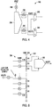
- FIG. 1 shows a simplified block diagram of a dual string DAC 100.
- the dual string DAC 100 includes a most significant bits (MSB) String 120 and a least significant bits (LSB) String 130, which both include series-coupled impedance strings, such as resistor strings.
- a digital signal processor (DSP) 140 receives a digital input signal Din and outputs control signals C 0 -C N to control the MSB String 120 and control signals D 0 -D M to control the LSB String 130.
- the MSB String 120 typically converts the most significant bits (MSBs) of the digital word, and its output is coupled to the LSB String 130, which converts the least significant bits (LSBs) of the digital word.
- VOUT represents the converted analog signal.
- FIG. 2 depicts an example of a schematic diagram of the dual string digital-to-analog converter 100 of FIG. 1 .
- each string 120, 130 include a resistor string 121.1-121.N, 131.1-131.M coupled to respective switch sets 122.0-122.N, 132.0-132.M that are operated according to digital word based control signals, C 0 -C N and D 0 -D M .
- the switches in switch sets 122.0-122.N, 132.0-132.M generally include only two states-on or off.
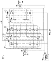
- the dual string DAC 100 is a single channel DAC. Multiple channel string DACs are disclosed in commonly assigned U.S. Patent No. 9,124,296 . Multiple string DACs are disclosed in commonly assigned U.S. Patent No. 9,100,045 . Another example of a multiple string DAC that can be used to implement the techniques of this disclosure is disclosed in commonly assigned U.S. Patent No. 5,969,657 .
- a multi-string DAC can also be considered a multi-stage DAC where at least two stages can include a string of impedance elements.
- a first stage uses a first string for converting an N-bit digital word, e.g., coarse conversion, and a second stage using a second string to further decode the N-bit digital word, e.g., finer conversion.
- N-bit digital word e.g., coarse conversion
- second stage uses a second string to further decode the N-bit digital word, e.g., finer conversion.
- resistors are an example of the type of impedance element that may be used and it is not intended to limit the present teaching to an implementation where resistors are used exclusively as impedance elements.
- resistors may be a preferred type of impedance element, particularly in scenarios where the voltage across the string is high-such as the string that is coupled to the reference terminals of the converter. In other strings where the voltage is relatively small, other elements such as active MOS devices may also be used.
- the present teaching should therefore not be construed as being limited to a multi-resistor string DAC.
- FIG. 3 is a schematic diagram showing an example of a multiple string, multiple output digital to analog converter circuit, in accordance with various techniques of this disclosure.
- the DAC circuit 200 can include a first impedance string 202, e.g., resistor string, including a plurality of first impedance elements 204, e.g., resistors, and a second impedance string 206, e.g., resistor string, including a plurality of second impedance elements 208, e.g., resistors.
- Each of the first impedance elements can have a first impedance, e.g., resistance, of R1.
- Each of the second impedance elements can have a second impedance, e.g., resistance, of R2.
- impedance R1 can be different than impedance R2.
- the DAC circuit 200 of FIG. 3 can include a first switching network RSW1 210 including a plurality of first switches 212 coupled to the first impedance string 202 and a second switching network RSW2 214 including a plurality of second switches 216 coupled to the second impedance string 206.
- the second switching network RSW2 can couple at least one of the second impedance elements to a first output node 218.
- every other switch 212 in the first switching network RSW1 can be coupled together.
- the switches in the first switching network RSW1 can be DC current carrying switches.
- the switches in the second switching network RSW1 can conduct substantially no DC current in normal operation and thus can be low leakage switches (or non-current carrying switches).
- the first impedance string 202 e.g., the main impedance string
- the second impedance string 206 e.g., secondary impedance string
- the first analog signal VOUT1 can have a first resolution, e.g., 12-bit resolution, where the first impedance string 202 can be used to convert the MSBs of the first digital input signal and the second impedance string 206 can be used to convert the LSBs of the first digital input signal.
- the circuit components grouped in 220 can be considered to represent a first DAC.
- the first impedance string 202 can be coupled to the DAC reference terminal and ground via additional impedance elements 222, 224, e.g., resistors. These additional elements 222, 224 can be useful for range tuning and in low and ultra-low power applications for sub-threshold leakage reduction.
- a control circuit 226, e.g., DSP can receive a first digital input signal and output control signals to control respective switching networks 210, 214 to control the MSB String 202 and the LSB String 206 to generate the first analog signal VOUT1. More particularly, the DSP can control the first switching network 210 to couple a voltage produced across at least one of the first impedance elements 204 across the second impedance string 206 in response to the first digital input signal, where the digital input signal includes a digital bit stream, e.g., digital word, having MSBs and LSBs.
- the impedance elements in the second impedance string 206 are configured to produce voltages in response to current passing from the first string 202 through the first switching network 210 to the second string 206 to produce a corresponding analog signal VOUT1 to the digital input signal to the first output node 218.
- the first and second impedance elements are configured to produce a first analog signal VOUT1 corresponding to the first digital input signal to the first output node 218.
- the DAC circuit 200 can provide a first analog output VOUT1, e.g., first DAC output, having a first resolution at the first output node 218 in response to a first digital input signal.
- the first output node 218 can be coupled to an optional switch 228.
- this disclosure describes techniques to provide a second analog output VOUT2, e.g., second DAC output, in response to a second digital input signal, having a second resolution at a second output node 230, using a shared impedance string, e.g., the first impedance string 202.
- the shared impedance string 202 can be used to generate multiple outputs having different resolutions, e.g., a first DAC output VOUT1 at 12-bit resolution and a second DAC output VOUT2 at a 6-bit resolution.
- the circuit components grouped in 234 can be considered to represent a second DAC.
- the control circuit 226, e.g., a DSP can control a third switching network RSW3 232 to couple a voltage produced across at least one of the first impedance elements 204 in response to a second digital input signal, e.g., a 6-bit digital input signal.
- a second digital input signal e.g., a 6-bit digital input signal.
- the first impedance elements 204 can be configured to produce a second analog signal VOUT2 corresponding to the second digital input signal to a second output node 230.
- the first analog signal VOUT1 at the first output node 218 can correspond to the MSBs and the LSBs of a first digital input signal
- the second analog signal VOUT2 at the second output node 230 can correspond to a second digital input signal
- the DAC circuit 200 of FIG. 3 can be considered to include a first DAC 220 having a first resolution, e.g., 12-bit resolution, and a second DAC 234 having a second resolution, e.g., 6-bit resolution, where the first output node 218 and the second output node 230 form multiple DAC outputs.
- the second output node 230 can be coupled to an optional switch 236.
- the resolutions of VOUT1 and VOUT2 are different, as in FIG. 3 .
- the first analog signal VOUT1 and the second analog signal VOUT2 can be used single ended. In some example implementations, and as described in more detail below, the first analog signal VOUT1 and the second analog signal VOUT2 can be used quasi-differentially. A quasi-differential implementation is not fully symmetric as would be a fully differential implementation due to the differing resolutions.
- the switches of the switching networks described in this disclosure can be implemented using transistors including, but not limited to, field-effect transistors (FETs), such as metal-oxide-semiconductor (MOS) FETs, FinFETs, gate-all-around (GAA) FETs, etc.
- FETs field-effect transistors
- MOS metal-oxide-semiconductor
- GAA gate-all-around
- the switches of the switching networks described in this disclosure can be implemented using microelectromechanical systems (MEMS) or nanoelectromechanical systems (NEMS).
- MEMS microelectromechanical systems
- NEMS nanoelectromechanical systems
- the circuits described in this disclosure can be integrated on an integrated circuit.
- FIG. 3 depicts two outputs, this disclosure is not limited to such a configuration. Rather, the circuit 200 of FIG. 3 can be configured to provide more than two outputs.
- FIG. 4 is a schematic diagram showing an example of a multiplexer circuit configuration, in accordance with various techniques of this disclosure.
- the DAC circuit 200 e.g., of FIG. 3
- each of the two DAC outputs VOUT1 and VOUT2 can be coupled, e.g., via optional switches 238, 240, to both first and second multiplexers 242, 244.
- the internal configurations of the first and second multiplexers 242, 244 can allow the two DAC outputs VOUT1 and VOUT2 to be multiplexed, swapped, or chopped.
- a control circuit can control the first and second multiplexers 242, 244 of FIG. 4 to generate a pair of signals, including, for example, VOUT1/VOUT1, VOUT2/VOUT2, VOUT1/VOUT2, and VOUT2/VOUT1.
- the circuit 246 of FIG. 4 can include switch 248 coupled to the VREF terminal in this single ended example configuration, e.g., for power-down.
- FIG. 4 is a simplified functional representation.
- S/H sample-and-hold
- Optional switches 238, 240 can be used for explicit sample-and-hold purposes as shown, enabling isolating DAC core settling activity. Similar functionality, but without isolation, can be achieved via switching networks RSW2 and RSW3 on their own, via merging digital switch controls.
- the optional switches 238, 240 can be explicit switches, inside or outside the DAC core sub-block.
- the optional switches 238, 240 can be used for sample-and-hold or break-before-make (BBM) switching functions.
- BBM break-before-make
- FIGS. 5 and 6 depict schematic diagrams illustrating the crosstalk problem to be solved.
- the present inventors have recognized that sharing a common impedance string 202 can result in an interaction, or crosstalk, between the two DACs 220, 234, when buffers are not used to buffer DAC 220.
- the second impedance string 206 can try to pull up or pull down the second DAC output VOUT2, e.g., the 6-bit output, because of the loading on the first string 202.
- the crosstalk between the DAC outputs is described below with respect to FIGS. 5 and 6 .
- FIG. 5 is a schematic diagram showing an example of a multiple string, multiple output digital to analog converter circuit, in accordance with various techniques of this disclosure, with crosstalk between the two DACs. More particularly, FIG. 5 is a simplified version of FIG. 3 of a first configuration in which the network of impedance elements of the first DAC 220 of FIG. 3 is above the network of impedance elements of the second DAC 234 of FIG. 3 .
- the first DAC 220 formed by the first impedance string 202 and the second impedance string 206 of FIG. 3 , loads the first string 202.
- the first DAC 220 can pull up the second DAC output VOUT2 by an amount + ⁇ V1.
- FIG. 6 is a schematic diagram showing another example of a multiple string, multiple output digital to analog converter circuit, in accordance with various techniques of this disclosure, with crosstalk between the two DACs. More particularly, FIG. 6 is a simplified version of FIG. 3 of a first configuration in which the network of impedance elements of the first DAC 220 of FIG. 3 is below the network of impedance elements of the second DAC 234 of FIG. 3 .
- the first DAC 220 formed by the first impedance string 202 and the second impedance string 206 of FIG. 3 , loads the first string 202.
- the first DAC 220 can pull down the second DAC output VOUT2 by an amount - ⁇ V2.
- the present inventors have resolved and substantially cancelled out the crosstalk problem by including a loading compensation circuit to selectively adjust a pull-up or a pull-down of one of the first and second impedance elements to compensate for a loading by the other of the first and second impedance elements.
- the known specifics of the DAC architecture and design can dictate the loading effects. Given that the DAC digital inputs can correspond to the position and loading of the DACs on the first impedance string, the relative location of the first and second DACs 220, 234 can be detected digitally.
- the present inventors have solved the problem using switched loading compensation circuit solutions that can be used to compensate for or substantially cancel out the DACs' relative code dependent, architecture and design dependent interaction above and below the cross-over threshold.
- a control circuit e.g., DSP
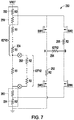
- FIG. 7 is a schematic diagram showing an example of a switched impedance solution to reduce crosstalk between two DACs.
- a control circuit e.g., control circuit 226 of FIG. 3
- the loading compensation circuit 250 of FIG. 7 can include additional switches, e.g., switches SW1-SW4, and additional impedance elements, 252, 254, and 256.
- the loading compensation circuit 250 is shown coupling into the impedances (of FIG. 3 ) between the DAC string terminals and the reference terminals (Vref+ and ground), above and below the DAC impedance string.
- the first impedance string 202 can be coupled to the DAC reference terminals and the ground via additional impedance elements 222, 224 of FIG. 3 , e.g., resistors.
- the control circuit can control the switches SW1-SW4 to add impedance elements in parallel with the upper impedance element 222 or the lower impedance element 224 to cancel the loading effect.
- first and second impedance elements 204, 208 can be placed in parallel with the upper resistor divider 258 or lower resistor divider 260 by controlling the four switches SW1-SW4 to compensate for a loading by the other of the first and second impedance elements.
- non-unit elements may be used. e.g., to save are.
- second impedance elements R2 can be placed in parallel with the upper resistor divider 258 or lower resistor divider 260 using switches SW1-SW4. In this manner, the loading compensation circuit of FIG. 7 can be a passive solution to the crosstalk problem.
- a switch control signal can be generated from a dynamic comparison result of the 6 MSB of the 12-bit input code of the first digital signal (12bit[11:0]) and the 6-bit input code of the second digital signal (6bit[5:0]) to make sure the load effect of upper and lower resistor string is the same.
- the following example control logic can be used to control the switches in such a configuration:
- break-before-make (BBM) switching can be used to avoid any shoot-through current that can otherwise occur when the SW1-SW4 data changes, due to differences in signal paths' delay as well as finite and variable turn on and off times.
- Impedance elements 252, 256 can be used to limit the current when discharging node A from close to VREF to ground and when charging node B from close to ground to VREF.
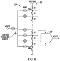
- FIG. 8 is a schematic diagram showing an example of a switched current solution to reduce crosstalk between two DACs.
- the loading compensation circuit 270 of FIG. 8 can be an active solution to the crosstalk problem.
- a switched current solution can be used to generate a current to effect an anti-crosstalk modulation similar to the switched impedance solution of FIG. 7 .
- the loading compensation circuit 270 is shown coupling into the impedances (of FIG. 3 ) between the DAC string terminals and the reference terminals (Vref+ and ground), above and below the DAC impedance string.
- Current sources and sinks are known to those of ordinary skill in the art, as are current mirrors, or current replicators. Current sources and current sinks are generally of one polarity and current mirrors can be used to make one current source/sink change polarity if desired, reflecting the current using a common-mode level. Alternately, a separate current source 272 and current sink 274 can be switched using a switching network having switches 276, 278 to achieve the same function, as shown in the example loading compensation circuit 270 of FIG. 8 .
- a current source or current sink sub-block may use the same voltage reference levels and the same impedance material or use a unit resistor as the DAC networks to enable tracking with the reference levels and impedance value, e.g., resistor value, tracking with variation such as process and temperature.
- a switched current sink 274 can be coupled above the DAC at the upper resistor divider 258 and a switched current source 272 can be coupled below the DAC at the lower resistor divider 260, as shown in FIG. 8 .
- the switched current sink 274 and the switched current source 272 can be coupled to one or more nodes within the DAC.
- Some example configurations can include aspects of both the loading compensation circuits of FIGS. 7 and 8 , e.g., both switched impedance and switched current solutions.
- a current source can output positive or negative current to perform a source or sink function.
- a current source can be used generally to describe a high impedance current output element that outputs positive or negative current.
- FIG. 9 is a schematic diagram showing an example of an application of the multiple string, multiple output DAC circuit 200 of FIG. 3 , in accordance with various techniques of this disclosure.
- the DAC circuit 200 (of FIG. 3 ) can receive digital input signals from digital control unit 280.
- the DAC circuit 280 can receive a first digital input signal, e.g., 12-bit digital input signal DIN12b[11:0], and a second digital input signal, e.g., 6-bit digital input DIN6b[5:0], and output respective analog output signals VOUT1 and VOUT2 having first and second resolutions.
- the first analog output signal VOUT1 can be provided to a non-inverting input of an amplifier 282, the output of which providing an excitation signal to a first electrode of a sensor 284, such as to the counter electrode (CE).
- An inverting input of the amplifier 282 can be coupled to a second electrode of the sensor 284, such as a reference electrode RE.
- the sensor 284 can be, for example, an electrochemical sensor used for various applications, such as for sensing the presence of one or more constituent gases, such as oxygen, carbon monoxide, etc., in an environment around the electrochemical sensor.
- the second analog output signal VOUT2 can be provided to a non-inverting input of a transimpedance amplifier 286.
- An inverting input of the transimpedance amplifier 286 can receive an output current of a sensing electrode (SE) of the sensor 284.
- An inverting input of the transimpedance amplifier 286 can be coupled to the sensing electrode (SE) of the sensor 284 by, for example, a load resistor R LOAD , or otherwise.
- the transimpedance amplifier 286 can be configured with a feedback resistor, R TIA , in a feedback path between the output of the transimpedance amplifier 286 and the inverting input of the transimpedance amplifier 286.
- the output of the transimpedance amplifier 286 and the input to the inverting terminal of the transimpedance amplifier 286 can be coupled to an analog-to-digital converter (ADC) (not shown).
- ADC analog-to-digital converter
- FIG. 10 is an example of a flow diagram of a method 300 of converting a first digital input string to a corresponding first analog signal having a first resolution and converting a second digital input string to a corresponding second analog signal having a second resolution, in accordance with this disclosure.
- the method 300 can include providing a multiple output digital-to-analog converter (DAC) circuit, the DAC circuit comprising a first string, e.g., string 202 of FIG. 3 , of first impedance elements and a second string, e.g., string 206 of FIG. 3 , of second impedance elements.
- DAC digital-to-analog converter
- the method 300 can include controlling, in response to a first digital input signal, a first switching network to couple a voltage produced across at least one of the first impedance elements across the second string to a first output node, the first digital input signal comprising a first digital bit stream having most significant bits (MSBs) and least significant bits (LSBs), the second impedance elements configured to produce a first analog signal corresponding to the first digital input signal.
- a control circuit e.g., control circuit 226 of FIG. 3
- the impedance elements of the first string 202 and the second string 206 can produce a first analog signal VOUT1 corresponding to the first digital input signal.
- the method 300 can include controlling, in response to a second digital input signal, a second switching network to couple a voltage produced across at least one of the first impedance elements to a second output node, the first impedance elements configured to produce a second analog signal corresponding to the second digital input signal, where the first output node and the second output node form multiple outputs.
- a control circuit e.g., control circuit 226 of FIG.
- the second switching network 232 can control the second switching network 232 to couple a voltage produced across at least one of the impedance elements of the first string 202 to the second output node 230 in response to a second digital input signal, e.g., a 6-bit signal, to produce a second analog signal VOUT2 corresponding to the second digital input signal.
- a second digital input signal e.g., a 6-bit signal
- the method 300 of FIG. 10 can optionally further include controlling a loading compensation circuit to selectively adjust a pull-up or a pull-down of one of the first and second impedance elements to compensate for a loading by the other of the first and second impedance elements.
- controlling the loading compensation circuit can include providing one or more anti-crosstalk impedance elements, and controlling a third switching network to couple the one or more anti-crosstalk impedance elements in parallel with at least one of the second impedance elements.
- controlling the loading compensation circuit can include providing at least one current source, and controlling a third switching network to couple the at least one current source to the second string.
- controlling the loading compensation circuit can include controlling the loading compensation circuit using a comparison between the MSBs of the first digital input signal and the second digital input signal.
- the method 300 of FIG. 10 can optionally further include controlling a fourth switching network, e.g., switching network RSW2 of FIG. 3 , to couple at least one of the second impedance elements to the first output node.
- a fourth switching network e.g., switching network RSW2 of FIG. 3
- the method 300 of FIG. 10 can optionally further include providing a first multiplexer having a first input and a second input, providing a second multiplexer having a first input and a second input, where the first input of the first multiplexer is coupled to the first output node and configured to receive the first analog signal, where the first input of the second multiplexer is coupled to the second output node and configured to receive the second analog signal, where the first input of the first multiplexer is coupled to the second input of the second multiplexer, and where the first input of the second multiplexer is coupled to the second input of the first multiplexer, and controlling the first and second multiplexers to output a pair of signals.
- Method examples described herein may be machine or computer-implemented at least in part. Some examples may include a computer-readable medium or machine-readable medium encoded with instructions operable to configure an electronic device to perform methods as described in the above examples.
- An implementation of such methods may include code, such as microcode, assembly language code, a higher-level language code, or the like. Such code may include computer readable instructions for performing various methods. The code may form portions of computer program products. Further, in an example, the code may be tangibly stored on one or more volatile, non-transitory, or non-volatile tangible computer-readable media, such as during execution or at other times.
- tangible computer-readable media may include, but are not limited to, hard disks, removable magnetic disks, removable optical disks (e.g., compact discs and digital video discs), magnetic cassettes, memory cards or sticks, random access memories (RAMs), read only memories (ROMs), and the like.
Landscapes
- Engineering & Computer Science (AREA)
- Theoretical Computer Science (AREA)
- Chemical & Material Sciences (AREA)
- Health & Medical Sciences (AREA)
- Life Sciences & Earth Sciences (AREA)
- Physics & Mathematics (AREA)
- Biochemistry (AREA)
- General Physics & Mathematics (AREA)
- Pathology (AREA)
- Analytical Chemistry (AREA)
- Immunology (AREA)
- General Health & Medical Sciences (AREA)
- Molecular Biology (AREA)
- Electrochemistry (AREA)
- Chemical Kinetics & Catalysis (AREA)
- Combustion & Propulsion (AREA)
- Food Science & Technology (AREA)
- Medicinal Chemistry (AREA)
- Analogue/Digital Conversion (AREA)
- Electromagnetism (AREA)
Claims (13)
- Digital/Analog-Umsetzerschaltung, DAC-Schaltung, (200) mit mehreren Ausgängen, die wenigstens zwei analoge Ausgangssignale mit unterschiedlicher Auflösung bereitstellt, wobei die DAC-Schaltung Folgendes umfasst:eine erste Reihe (202) erster Impedanzelemente (204);eine zweite Reihe (206) zweiter Impedanzelemente (208);ein erstes Schaltnetz (210), das in Reaktion auf ein erstes digitales Eingangssignal eine Spannung, die über wenigstens einem der ersten Impedanzelemente erzeugt wird, über die zweite Reihe mit einem ersten Ausgangsknoten (218) koppelt, wobei das erste digitale Eingangssignal einen ersten digitalen Bitstrom mit höchstwertigen Bits, MSB, und niedrigstwertigen Bits, LSB, enthält, wobei die zweiten Impedanzelemente konfiguriert sind, ein erstes analoges Signal zu erzeugen, das dem ersten digitalen Eingangssignal entspricht; undein zweites Schaltnetz (232), das in Reaktion auf ein zweites digitales Eingangssignal eine Spannung, die über wenigstens einem der ersten Impedanzelemente erzeugt wird, mit einem zweiten Ausgangsknoten (230) koppelt, wobei die ersten Impedanzelemente konfiguriert sind, ein zweites analoges Signal, das dem zweiten digitalen Eingangssignal entspricht, zu erzeugen,wobei der erste Ausgangsknoten und der zweite Ausgangsknoten mehrere Ausgänge bilden,dadurch gekennzeichnet, dass:
für das erste und das zweite analoge Ausgangssignal durch Koppeln einer unterschiedlichen Anzahl von Reihen mit dem ersten bzw. dem zweiten Ausgangsknoten unterschiedliche Auflösungen bereitgestellt werden. - DAC-Schaltung nach Anspruch 1, wobei die Schaltung Folgendes umfasst:
eine Lastkompensationsschaltung, um wahlweise ein Hochziehen oder ein Herunterziehen eines der ersten und zweiten Impedanzelemente einzustellen, um eine Last durch das andere der ersten und zweiten Impedanzelemente zu kompensieren. - DAC-Schaltung (200) nach Anspruch 2, wobei die Lastkompensationsschaltung (250) Folgendes umfasst:ein oder mehrere Impedanzelemente, R2; undein drittes Schaltnetz, SW1-SW4, um das eine oder die mehreren Impedanzelemente mit wenigstens einem der zweiten Impedanzelemente parallel zu schalten.
- DAC-Schaltung (200) nach Anspruch 2 oder Anspruch 3, wobei die Lastkompensationsschaltung (270) Folgendes umfasst:wenigstens eine Stromquelle (272); undein drittes Schaltnetz (278), um die wenigstens eine Stromquelle mit der zweiten Reihe zu koppeln.
- DAC-Schaltung (200) nach einem der Ansprüche 2 bis 4, die Folgendes umfasst:
eine Steuerschaltung (226), die konfiguriert ist, die Lastkompensationsschaltung unter Verwendung eines Vergleichs zwischen den MSB des ersten digitalen Eingangssignals und des zweiten digitalen Eingangssignals zu steuern. - DAC-Schaltung (200) nach einem vorhergehenden Anspruch, die Folgendes umfasst:einen ersten Multiplexer (242) mit einem ersten Eingang und einem zweiten Eingang; undeinen zweiten Multiplexer (244) mit einem ersten Eingang und einem zweiten Eingang,wobei der erste Eingang des ersten Multiplexers mit dem ersten Ausgangsknoten gekoppelt ist und konfiguriert ist, das erste analoge Eingangssignal zu empfangen,wobei der erste Eingang des zweiten Multiplexers mit dem zweiten Ausgangsknoten gekoppelt ist und konfiguriert ist, das zweite Eingangssignal zu empfangen,wobei der zweite Eingang des ersten Multiplexers mit dem ersten Eingang des zweiten Multiplexers gekoppelt ist undwobei der zweite Eingang des zweiten Multiplexers mit dem ersten Eingang des ersten Multiplexers gekoppelt ist.
- DAC-Schaltung (200) nach einem vorhergehenden Anspruch, die wenigstens eines der folgenden Merkmale aufweist:(a) die ersten Impedanzelemente (204) enthalten erste Widerstände, wobei jeder erste Widerstand einen ersten Widerstandswert besitzt, wobei die zweiten Impedanzelemente (208) zweite Widerstände enthalten, wobei jeder zweite Widerstand einen zweiten Widerstandswert besitzt;(b) die DAC-Schaltung umfasst ferner ein viertes Schaltnetz (214), um wenigstens eines der zweiten Impedanzelemente mit dem ersten Ausgangsknoten (218) zu koppeln;(c) der erste Ausgangsknoten ist ein Ausgangsknoten eines ersten DAC, wobei der zweite Ausgangsknoten ein Ausgangsknoten eines zweiten DAC ist und wobei der erste DAC und der zweite DAC die erste Reihe gemeinsam nutzen.
- Verfahren zum Umsetzen einer ersten digitalen Eingangsreihe mit einem entsprechenden ersten analogen Signal, das eine erste Auflösung besitzt, und zum Umsetzen einer zweiten digitalen Eingangsreihe mit einem entsprechenden zweiten analogen Signal, das eine zweite Auflösung besitzt, wobei das Verfahren Folgendes umfasst:Bereitstellen (302) einer Digital/Analog-Umsetzerschaltung, DAC-Schaltung, (200) mit mehreren Ausgängen, wobei die DAC-Schaltung eine erste Reihe (202) erster Impedanzelemente (204) und eine zweite Reihe (206) zweiter Impedanzelemente (208) enthält;Steuern (304) in Reaktion auf ein erstes digitales Eingangssignal eines ersten Schaltnetzes (210), um eine Spannung, die über wenigstens einem der ersten Impedanzelemente erzeugt wird, über die zweite Reihe mit einem ersten Ausgangsknoten (218) zu koppeln, wobei das erste digitale Eingangssignal einen ersten digitalen Bitstrom mit höchstwertigen Bits, MSB, und niedrigstwertigen Bits, LSB, enthält, wobei die zweiten Impedanzelemente konfiguriert sind, ein erstes analoges Signal, das dem ersten digitalen Eingangssignal entspricht, zu erzeugen; undSteuern (306) in Reaktion auf ein zweites digitales Eingangssignal eines zweiten Schaltnetzes (232), um eine Spannung, die über wenigstens einem der ersten Impedanzelemente erzeugt wird, mit einem zweiten Ausgangsknoten (230) zu koppeln, wobei die ersten Impedanzelemente konfiguriert sind, ein zweites analoges Signal, das dem zweiten digitalen Eingangssignal entspricht, zu erzeugen,wobei der erste Ausgangsknoten und der zweiten Ausgangsknoten mehrere Ausgangsknoten bilden,dadurch gekennzeichnet, dassfür das erste und das zweite analoge Ausgangssignal durch Koppeln einer unterschiedlichen Anzahl von Reihen mit dem ersten bzw. dem zweiten Ausgangsknoten unterschiedliche Auflösungen bereitgestellt werden.
- Verfahren nach Anspruch 8, das ferner Folgendes umfasst:
Steuern einer Lastkompensationsschaltung (250, 270), um wahlweise ein Hochziehen oder ein Herunterziehen eines der ersten und zweiten Impedanzelemente einzustellen, um eine Last durch das andere der ersten und zweiten Impedanzelemente zu kompensieren. - Verfahren nach Anspruch 9, wobei das Steuern der Lastkompensationsschaltung wenigstens einen der folgenden Schritte umfasst:(a) Bereitstellen eines oder mehrerer Impedanzelemente, R2; und
Steuern eines dritten Schaltnetzes, SW1-SW4, um das eine oder die mehreren Impedanzelemente wenigstens mit der zweiten Impedanzelemente parallel zu schalten; und/oder(b) Bereitstellen wenigstens einer Stromquelle (272); und
Steuern eines dritten Schaltnetzes (278), um die wenigstens eine Stromquelle mit der zweiten Reihe zu koppeln; und/oder(c) Steuern der Lastkompensationsschaltung unter Verwendung eines Vergleichs zwischen den MSB des ersten digitalen Eingangssignals und des zweiten digitalen Eingangssignals. - Verfahren nach einem der Ansprüche 8 bis 10, das Folgendes umfasst:
Steuern eines vierten Schaltnetzes (214), um wenigstens eines der zweiten Impedanzelemente mit dem ersten Ausgangsknoten zu koppeln. - Verfahren nach einem der Ansprüche 8 bis 11, das Folgendes umfasst:Bereitstellen eines ersten Multiplexers (242) mit einem ersten Eingang und einem zweiten Eingang; undBereitstellen eines zweiten Multiplexers (244) mit einem ersten Eingang und einem zweiten Eingang,wobei der erste Eingang des ersten Multiplexers mit dem ersten Ausgangsknoten gekoppelt ist und konfiguriert ist, das erste analoge Eingangssignal zu empfangen,wobei der erste Eingang des zweiten Multiplexers mit dem zweiten Ausgangsknoten gekoppelt ist und konfiguriert ist, das zweite analoge Eingangssignal zu empfangen,wobei der zweite Eingang des ersten Multiplexers mit dem ersten Eingang des zweiten Multiplexers gekoppelt ist undwobei der zweite Eingang des zweiten Multiplexers mit dem ersten Eingang des ersten Multiplexers gekoppelt ist; undSteuern des ersten und des zweiten Multiplexers, um ein Paar Signale auszugeben.
- Elektrochemische Erfassungsschaltung, die Folgendes umfasst:eine Digital/Analog-Umsetzerschaltung, DAC-Schaltung, (200) mit mehreren Ausgängen nach einem der Ansprüche 1-7 undeinen elektrochemischen Sensor, der mit dem ersten Ausgangsknoten und/oder mit dem zweiten Ausgangsknoten der DAC-Schaltung gekoppelt ist.
Priority Applications (1)
| Application Number | Priority Date | Filing Date | Title |
|---|---|---|---|
| PL18170251T PL3399650T3 (pl) | 2017-05-04 | 2018-05-01 | Wielołańcuchowy, wielowyjściowy przetwornik cyfrowo-analogowy |
Applications Claiming Priority (1)
| Application Number | Priority Date | Filing Date | Title |
|---|---|---|---|
| US15/586,848 US9941894B1 (en) | 2017-05-04 | 2017-05-04 | Multiple string, multiple output digital to analog converter |
Publications (2)
| Publication Number | Publication Date |
|---|---|
| EP3399650A1 EP3399650A1 (de) | 2018-11-07 |
| EP3399650B1 true EP3399650B1 (de) | 2021-03-24 |
Family
ID=61801592
Family Applications (1)
| Application Number | Title | Priority Date | Filing Date |
|---|---|---|---|
| EP18170251.5A Active EP3399650B1 (de) | 2017-05-04 | 2018-05-01 | Mehrfach-ausgabe-digital-analog-wandler mit mehrfachketten |
Country Status (5)
| Country | Link |
|---|---|
| US (1) | US9941894B1 (de) |
| EP (1) | EP3399650B1 (de) |
| JP (1) | JP6732838B2 (de) |
| CN (1) | CN108809316B (de) |
| PL (1) | PL3399650T3 (de) |
Families Citing this family (11)
| Publication number | Priority date | Publication date | Assignee | Title |
|---|---|---|---|---|
| US10069414B2 (en) | 2015-04-01 | 2018-09-04 | Infineon Technologies Austria Ag | Switching voltage regulator input voltage and current sensing |
| US10389242B2 (en) | 2017-02-01 | 2019-08-20 | Infineon Technologies Austria Ag | Voltage and current sensing calibration for switching voltage regulators |
| US10224812B1 (en) * | 2017-10-13 | 2019-03-05 | Infineon Technologies Austria Ag | Sensing network mismatch compensation for switching voltage regulator with input voltage and current sensing |
| US10574247B1 (en) | 2018-09-14 | 2020-02-25 | Analog Devices Global Unlimited Company | Digital-to-analog converter transfer function modification |
| US11022629B2 (en) * | 2019-07-29 | 2021-06-01 | Analog Devices, Inc. | Low-glitch range change techniques |
| US11272854B1 (en) * | 2020-09-02 | 2022-03-15 | Analog Devices International Unlimited Company | Noise cancellation in impedance measurement circuits |
| TWI780780B (zh) * | 2021-06-18 | 2022-10-11 | 新唐科技股份有限公司 | 信號產生電路、微控制器及控制方法 |
| CN114584149B (zh) * | 2022-03-03 | 2025-06-27 | 江苏谷泰微电子有限公司 | 模数转换器 |
| US12483265B2 (en) * | 2022-11-29 | 2025-11-25 | Nxp Usa, Inc. | RDAC ladder with adaptive biasing to reduce the reference variation across temperature |
| US20240291488A1 (en) * | 2023-02-27 | 2024-08-29 | Stmicroelectronics International N.V. | Voltage compensation of differential voltage swing |
| CN118868939B (zh) * | 2024-09-25 | 2025-02-14 | 杭州晶华微电子股份有限公司 | 一种应用于ldo的电阻修调网络及集成电路 |
Family Cites Families (44)
| Publication number | Priority date | Publication date | Assignee | Title |
|---|---|---|---|---|
| EP0288215B1 (de) | 1987-04-24 | 1993-03-10 | Simmonds Precision Products Inc. | Bestimmung von elektrischer Kapazität und elektrischem Widerstand |
| GB9014679D0 (en) | 1990-07-02 | 1990-08-22 | Sarnoff David Res Center | Sequential successive approximation a/d converter |
| US5111205A (en) * | 1990-12-18 | 1992-05-05 | Vlsi Technology, Inc. | Digital-to-analog and analog-to-digital converters |
| JPH05175849A (ja) * | 1991-06-18 | 1993-07-13 | Fujitsu Ltd | Daコンバータ |
| SE500357C2 (sv) | 1992-01-31 | 1994-06-06 | Silicon Construction Sweden Ab | Arrangemang för analog/digital-omvandling |
| US5495245A (en) | 1994-04-26 | 1996-02-27 | Analog Devices, Inc. | Digital-to-analog converter with segmented resistor string |
| JP3433337B2 (ja) * | 1995-07-11 | 2003-08-04 | 日本テキサス・インスツルメンツ株式会社 | 液晶ディスプレイ用信号線駆動回路 |
| US5969657A (en) | 1997-07-22 | 1999-10-19 | Analog Devices, Inc. | Digital to analog converter |
| US6163289A (en) | 1997-09-23 | 2000-12-19 | Philips Electronics North America Corp. | Differential voltage digital-to-analog converter |
| JPH11211692A (ja) * | 1998-01-20 | 1999-08-06 | Denso Corp | 酸素濃度センサの素子インピーダンス検出装置 |
| US6128359A (en) * | 1998-10-27 | 2000-10-03 | Intel Corporation | Phase difference magnifier |
| JP2000286707A (ja) * | 1999-03-30 | 2000-10-13 | Toshiba Corp | デジタル−アナログ変換器およびこれを用いた液晶ディスプレイ装置 |
| WO2001020358A1 (en) | 1999-09-17 | 2001-03-22 | Delphi Technologies, Inc. | Method and apparatus for calibrating a current sensing system |
| US6448916B1 (en) * | 2000-05-31 | 2002-09-10 | Cygnal Integrated Products, Inc. | Dual sub-DAC resistor strings with analog interpolation |
| US6414616B1 (en) | 2000-06-22 | 2002-07-02 | Analog Devices, Inc. | Architecture for voltage scaling DAC |
| TW453045B (en) * | 2000-10-09 | 2001-09-01 | Winbond Electronics Corp | Multi-level pulse width modulation device and its control structure |
| US6695475B2 (en) | 2001-05-31 | 2004-02-24 | Stmicroelectronics, Inc. | Temperature sensing circuit and method |
| KR100497991B1 (ko) | 2002-07-29 | 2005-07-01 | 세주엔지니어링주식회사 | 휴대용 가스 검출기 및 그의 재기초화 방법 |
| US6778122B2 (en) | 2002-12-23 | 2004-08-17 | Institute Of Microelectronics | Resistor string digital to analog converter with differential outputs and reduced switch count |
| US6995701B1 (en) * | 2004-03-02 | 2006-02-07 | Maxim Integrated Products, Inc. | Multichannel high resolution segmented resistor string digital-to-analog converters |
| DE602005019457D1 (de) * | 2004-11-12 | 2010-04-01 | Mediatek Inc | System und verfahren für einen ausgeglichenen digital-analog-wandler mit zweifacher widerstandsfolge |
| US7109904B2 (en) | 2004-12-21 | 2006-09-19 | Exar Corporation | High speed differential resistive voltage digital-to-analog converter |
| JP2006279132A (ja) * | 2005-03-28 | 2006-10-12 | Yamaha Corp | D/aコンバータの試験装置およびその試験方法 |
| US7136002B2 (en) | 2005-04-15 | 2006-11-14 | Analog Devices, Inc. | Digital to analog converter |
| US7339508B2 (en) | 2006-06-23 | 2008-03-04 | Analog Devices, Inc. | Digital to analog converter with shared calibration |
| US7504979B1 (en) * | 2006-08-21 | 2009-03-17 | National Semiconductor Corporation | System and method for providing an ultra low power scalable digital-to-analog converter (DAC) architecture |
| JP4779875B2 (ja) * | 2006-08-24 | 2011-09-28 | ソニー株式会社 | ディジタル−アナログ変換器および映像表示装置 |
| US7501970B2 (en) * | 2006-10-30 | 2009-03-10 | Texas Instruments Incorporated | Digital to analog converter architecture and method having low switch count and small output impedance |
| JP4958699B2 (ja) * | 2007-09-10 | 2012-06-20 | オンセミコンダクター・トレーディング・リミテッド | D/aコンバータ、逐次比較型a/dコンバータ |
| US7583216B2 (en) * | 2007-09-28 | 2009-09-01 | Sigmatel, Inc. | Adjustable DAC and applications thereof |
| CN101471669A (zh) * | 2007-12-28 | 2009-07-01 | 上海华虹Nec电子有限公司 | 数模转换器和数模转换方法 |
| CN101242186B (zh) * | 2008-03-18 | 2010-10-06 | 苏州纳米技术与纳米仿生研究所 | 一种可编程的非线性数模转换器 |
| SE533293C2 (sv) | 2008-10-10 | 2010-08-17 | Zoran Corp | Analog/digital-omvandlare |
| US8337082B2 (en) | 2009-05-08 | 2012-12-25 | Canon U.S. Life Sciences, Inc. | Systems and methods for auto-calibration of resistive temperature sensors |
| US7956786B2 (en) * | 2009-10-30 | 2011-06-07 | Analog Devices, Inc. | Digital-to-analogue converter |
| US8714816B2 (en) | 2010-09-12 | 2014-05-06 | Medisim Ltd. | Temperature sensor with calibrated analog resistive output |
| US9124296B2 (en) | 2012-06-27 | 2015-09-01 | Analog Devices Global | Multi-stage string DAC |
| US9041375B2 (en) * | 2012-10-30 | 2015-05-26 | Infineon Technologies Ag | High resolution control for a multimode SMPS converter and high resolution slope generator |
| US9077376B2 (en) | 2013-03-15 | 2015-07-07 | Analog Devices Global | Multiple string digital to analog converter comprising a control circuit |
| US8884799B2 (en) * | 2013-03-15 | 2014-11-11 | Qualcomm Incroporated | Dual-string digital-to-analog converters (DACs), and related circuits, systems, and methods |
| CN103368574A (zh) * | 2013-05-27 | 2013-10-23 | 苏州贝克微电子有限公司 | 数字模拟转换器 |
| CN104579349B (zh) * | 2013-10-11 | 2017-12-15 | 上海山景集成电路股份有限公司 | 基于偏移和共模补偿的电阻阶梯形数字模拟转换器 |
| US9407278B1 (en) | 2015-07-01 | 2016-08-02 | Analog Devices Global | Digital to analog converter |
| US9444487B1 (en) | 2015-08-27 | 2016-09-13 | Analog Devices Global | Multiple stage digital to analog converter |
-
2017
- 2017-05-04 US US15/586,848 patent/US9941894B1/en active Active
-
2018
- 2018-05-01 EP EP18170251.5A patent/EP3399650B1/de active Active
- 2018-05-01 PL PL18170251T patent/PL3399650T3/pl unknown
- 2018-05-04 CN CN201810420072.XA patent/CN108809316B/zh active Active
- 2018-05-07 JP JP2018089199A patent/JP6732838B2/ja active Active
Non-Patent Citations (1)
| Title |
|---|
| None * |
Also Published As
| Publication number | Publication date |
|---|---|
| CN108809316B (zh) | 2022-07-08 |
| PL3399650T3 (pl) | 2022-01-17 |
| JP6732838B2 (ja) | 2020-07-29 |
| US9941894B1 (en) | 2018-04-10 |
| EP3399650A1 (de) | 2018-11-07 |
| JP2018191291A (ja) | 2018-11-29 |
| CN108809316A (zh) | 2018-11-13 |
Similar Documents
| Publication | Publication Date | Title |
|---|---|---|
| EP3399650B1 (de) | Mehrfach-ausgabe-digital-analog-wandler mit mehrfachketten | |
| CN102771052B (zh) | 源极跟随器输入缓冲器 | |
| US9407278B1 (en) | Digital to analog converter | |
| EP2629428A1 (de) | Analog-Digital-Wandler und Verfahren zu dessen Kalibrierung | |
| CN101399522B (zh) | 多输入运算放大电路及使用其的数字/模拟转换器 | |
| US20130015996A1 (en) | Ad converter and information processing apparatus | |
| KR100550102B1 (ko) | 전류셀 구동 방식의 디지털-아날로그 변환기 | |
| CN104685790A (zh) | 用于减小流水线型adc的面积和功率的电路和方法 | |
| US10075179B1 (en) | Multiple string, multiple output digital to analog converter | |
| WO2013165976A2 (en) | Segmented digital-to-analog converter having weighted current sources | |
| US7224306B2 (en) | Analog-to-digital converter in which settling time of amplifier circuit is reduced | |
| WO2011104786A1 (ja) | パイプライン型a/dコンバータおよびa/d変換方法、ならびにダイナミック型差動増幅器 | |
| EP4391387A1 (de) | Techniken zur reduzierung von störungseffekten bei einem digital-analog-wandler | |
| JP3907633B2 (ja) | Nic回路及びadc回路 | |
| Koçak | A Low-power Succesive Approximation Register Analog-To-Digital Converter Integrated Circuit for Imaging Sensors | |
| Liu et al. | A highly energy-efficient switching scheme for SAR ADC with the redundant capacitance splitting technology | |
| US20120044103A1 (en) | Parallel interpolation a/d converter and digital equalizer | |
| Tang et al. | New fully-differential amplifier-less pipelined ADC with wide power scalability and ERBW | |
| KR101583292B1 (ko) | 아날로그-디지털 변환기의 동적 레지듀 증폭기 및 그 증폭 방법 | |
| JP5515126B2 (ja) | パイプライン型a/dコンバータおよびa/d変換方法、ならびにダイナミック型差動増幅器 | |
| Lin et al. | A 1-GS/s 6-bit folding and interpolating ADC in 0.13-μm CMOS | |
| Baek et al. | Scaled-down reference switching scheme for low-power SAR ADCs | |
| JP5639106B2 (ja) | D/a変換器 | |
| Park | A Design of 12-Bit 125ms/s 3-Bit/Cycle Sar-Based Pipeline Adc Employing a Novel Amplifier | |
| Mulder et al. | A 12-bit 800 MS/s Dual-Residue Pipeline ADC |
Legal Events
| Date | Code | Title | Description |
|---|---|---|---|
| PUAI | Public reference made under article 153(3) epc to a published international application that has entered the european phase |
Free format text: ORIGINAL CODE: 0009012 |
|
| STAA | Information on the status of an ep patent application or granted ep patent |
Free format text: STATUS: THE APPLICATION HAS BEEN PUBLISHED |
|
| AK | Designated contracting states |
Kind code of ref document: A1 Designated state(s): AL AT BE BG CH CY CZ DE DK EE ES FI FR GB GR HR HU IE IS IT LI LT LU LV MC MK MT NL NO PL PT RO RS SE SI SK SM TR |
|
| AX | Request for extension of the european patent |
Extension state: BA ME |
|
| STAA | Information on the status of an ep patent application or granted ep patent |
Free format text: STATUS: REQUEST FOR EXAMINATION WAS MADE |
|
| 17P | Request for examination filed |
Effective date: 20190501 |
|
| RBV | Designated contracting states (corrected) |
Designated state(s): AL AT BE BG CH CY CZ DE DK EE ES FI FR GB GR HR HU IE IS IT LI LT LU LV MC MK MT NL NO PL PT RO RS SE SI SK SM TR |
|
| GRAP | Despatch of communication of intention to grant a patent |
Free format text: ORIGINAL CODE: EPIDOSNIGR1 |
|
| STAA | Information on the status of an ep patent application or granted ep patent |
Free format text: STATUS: GRANT OF PATENT IS INTENDED |
|
| INTG | Intention to grant announced |
Effective date: 20201008 |
|
| RIN1 | Information on inventor provided before grant (corrected) |
Inventor name: WANG, HANQING Inventor name: DEMPSEY, DENNIS A. Inventor name: LIU, TONY YINCAI Inventor name: GU, SHURONG Inventor name: QU, GUANGYANG |
|
| GRAS | Grant fee paid |
Free format text: ORIGINAL CODE: EPIDOSNIGR3 |
|
| GRAA | (expected) grant |
Free format text: ORIGINAL CODE: 0009210 |
|
| STAA | Information on the status of an ep patent application or granted ep patent |
Free format text: STATUS: THE PATENT HAS BEEN GRANTED |
|
| AK | Designated contracting states |
Kind code of ref document: B1 Designated state(s): AL AT BE BG CH CY CZ DE DK EE ES FI FR GB GR HR HU IE IS IT LI LT LU LV MC MK MT NL NO PL PT RO RS SE SI SK SM TR |
|
| REG | Reference to a national code |
Ref country code: GB Ref legal event code: FG4D |
|
| REG | Reference to a national code |
Ref country code: CH Ref legal event code: EP |
|
| REG | Reference to a national code |
Ref country code: IE Ref legal event code: FG4D |
|
| REG | Reference to a national code |
Ref country code: DE Ref legal event code: R096 Ref document number: 602018014229 Country of ref document: DE Ref country code: AT Ref legal event code: REF Ref document number: 1375554 Country of ref document: AT Kind code of ref document: T Effective date: 20210415 |
|
| REG | Reference to a national code |
Ref country code: NL Ref legal event code: FP |
|
| RAP2 | Party data changed (patent owner data changed or rights of a patent transferred) |
Owner name: ANALOG DEVICES INTERNATIONAL UNLIMITED COMPANY |
|
| REG | Reference to a national code |
Ref country code: LT Ref legal event code: MG9D |
|
| PG25 | Lapsed in a contracting state [announced via postgrant information from national office to epo] |
Ref country code: NO Free format text: LAPSE BECAUSE OF FAILURE TO SUBMIT A TRANSLATION OF THE DESCRIPTION OR TO PAY THE FEE WITHIN THE PRESCRIBED TIME-LIMIT Effective date: 20210624 Ref country code: HR Free format text: LAPSE BECAUSE OF FAILURE TO SUBMIT A TRANSLATION OF THE DESCRIPTION OR TO PAY THE FEE WITHIN THE PRESCRIBED TIME-LIMIT Effective date: 20210324 Ref country code: FI Free format text: LAPSE BECAUSE OF FAILURE TO SUBMIT A TRANSLATION OF THE DESCRIPTION OR TO PAY THE FEE WITHIN THE PRESCRIBED TIME-LIMIT Effective date: 20210324 Ref country code: GR Free format text: LAPSE BECAUSE OF FAILURE TO SUBMIT A TRANSLATION OF THE DESCRIPTION OR TO PAY THE FEE WITHIN THE PRESCRIBED TIME-LIMIT Effective date: 20210625 Ref country code: BG Free format text: LAPSE BECAUSE OF FAILURE TO SUBMIT A TRANSLATION OF THE DESCRIPTION OR TO PAY THE FEE WITHIN THE PRESCRIBED TIME-LIMIT Effective date: 20210624 |
|
| PG25 | Lapsed in a contracting state [announced via postgrant information from national office to epo] |
Ref country code: LV Free format text: LAPSE BECAUSE OF FAILURE TO SUBMIT A TRANSLATION OF THE DESCRIPTION OR TO PAY THE FEE WITHIN THE PRESCRIBED TIME-LIMIT Effective date: 20210324 Ref country code: RS Free format text: LAPSE BECAUSE OF FAILURE TO SUBMIT A TRANSLATION OF THE DESCRIPTION OR TO PAY THE FEE WITHIN THE PRESCRIBED TIME-LIMIT Effective date: 20210324 Ref country code: SE Free format text: LAPSE BECAUSE OF FAILURE TO SUBMIT A TRANSLATION OF THE DESCRIPTION OR TO PAY THE FEE WITHIN THE PRESCRIBED TIME-LIMIT Effective date: 20210324 |
|
| REG | Reference to a national code |
Ref country code: AT Ref legal event code: MK05 Ref document number: 1375554 Country of ref document: AT Kind code of ref document: T Effective date: 20210324 |
|
| PG25 | Lapsed in a contracting state [announced via postgrant information from national office to epo] |
Ref country code: LT Free format text: LAPSE BECAUSE OF FAILURE TO SUBMIT A TRANSLATION OF THE DESCRIPTION OR TO PAY THE FEE WITHIN THE PRESCRIBED TIME-LIMIT Effective date: 20210324 Ref country code: EE Free format text: LAPSE BECAUSE OF FAILURE TO SUBMIT A TRANSLATION OF THE DESCRIPTION OR TO PAY THE FEE WITHIN THE PRESCRIBED TIME-LIMIT Effective date: 20210324 Ref country code: CZ Free format text: LAPSE BECAUSE OF FAILURE TO SUBMIT A TRANSLATION OF THE DESCRIPTION OR TO PAY THE FEE WITHIN THE PRESCRIBED TIME-LIMIT Effective date: 20210324 Ref country code: SM Free format text: LAPSE BECAUSE OF FAILURE TO SUBMIT A TRANSLATION OF THE DESCRIPTION OR TO PAY THE FEE WITHIN THE PRESCRIBED TIME-LIMIT Effective date: 20210324 Ref country code: AT Free format text: LAPSE BECAUSE OF FAILURE TO SUBMIT A TRANSLATION OF THE DESCRIPTION OR TO PAY THE FEE WITHIN THE PRESCRIBED TIME-LIMIT Effective date: 20210324 |
|
| REG | Reference to a national code |
Ref country code: GB Ref legal event code: 732E Free format text: REGISTERED BETWEEN 20211014 AND 20211020 |
|
| PG25 | Lapsed in a contracting state [announced via postgrant information from national office to epo] |
Ref country code: IS Free format text: LAPSE BECAUSE OF FAILURE TO SUBMIT A TRANSLATION OF THE DESCRIPTION OR TO PAY THE FEE WITHIN THE PRESCRIBED TIME-LIMIT Effective date: 20210724 Ref country code: PT Free format text: LAPSE BECAUSE OF FAILURE TO SUBMIT A TRANSLATION OF THE DESCRIPTION OR TO PAY THE FEE WITHIN THE PRESCRIBED TIME-LIMIT Effective date: 20210726 Ref country code: SK Free format text: LAPSE BECAUSE OF FAILURE TO SUBMIT A TRANSLATION OF THE DESCRIPTION OR TO PAY THE FEE WITHIN THE PRESCRIBED TIME-LIMIT Effective date: 20210324 Ref country code: RO Free format text: LAPSE BECAUSE OF FAILURE TO SUBMIT A TRANSLATION OF THE DESCRIPTION OR TO PAY THE FEE WITHIN THE PRESCRIBED TIME-LIMIT Effective date: 20210324 |
|
| REG | Reference to a national code |
Ref country code: CH Ref legal event code: PL |
|
| REG | Reference to a national code |
Ref country code: DE Ref legal event code: R097 Ref document number: 602018014229 Country of ref document: DE |
|
| PG25 | Lapsed in a contracting state [announced via postgrant information from national office to epo] |
Ref country code: ES Free format text: LAPSE BECAUSE OF FAILURE TO SUBMIT A TRANSLATION OF THE DESCRIPTION OR TO PAY THE FEE WITHIN THE PRESCRIBED TIME-LIMIT Effective date: 20210324 Ref country code: AL Free format text: LAPSE BECAUSE OF FAILURE TO SUBMIT A TRANSLATION OF THE DESCRIPTION OR TO PAY THE FEE WITHIN THE PRESCRIBED TIME-LIMIT Effective date: 20210324 Ref country code: DK Free format text: LAPSE BECAUSE OF FAILURE TO SUBMIT A TRANSLATION OF THE DESCRIPTION OR TO PAY THE FEE WITHIN THE PRESCRIBED TIME-LIMIT Effective date: 20210324 Ref country code: CH Free format text: LAPSE BECAUSE OF NON-PAYMENT OF DUE FEES Effective date: 20210531 Ref country code: LI Free format text: LAPSE BECAUSE OF NON-PAYMENT OF DUE FEES Effective date: 20210531 Ref country code: MC Free format text: LAPSE BECAUSE OF FAILURE TO SUBMIT A TRANSLATION OF THE DESCRIPTION OR TO PAY THE FEE WITHIN THE PRESCRIBED TIME-LIMIT Effective date: 20210324 Ref country code: LU Free format text: LAPSE BECAUSE OF NON-PAYMENT OF DUE FEES Effective date: 20210501 |
|
| PLBE | No opposition filed within time limit |
Free format text: ORIGINAL CODE: 0009261 |
|
| STAA | Information on the status of an ep patent application or granted ep patent |
Free format text: STATUS: NO OPPOSITION FILED WITHIN TIME LIMIT |
|
| REG | Reference to a national code |
Ref country code: BE Ref legal event code: MM Effective date: 20210531 |
|
| PG25 | Lapsed in a contracting state [announced via postgrant information from national office to epo] |
Ref country code: SI Free format text: LAPSE BECAUSE OF FAILURE TO SUBMIT A TRANSLATION OF THE DESCRIPTION OR TO PAY THE FEE WITHIN THE PRESCRIBED TIME-LIMIT Effective date: 20210324 |
|
| 26N | No opposition filed |
Effective date: 20220104 |
|
| PG25 | Lapsed in a contracting state [announced via postgrant information from national office to epo] |
Ref country code: IE Free format text: LAPSE BECAUSE OF NON-PAYMENT OF DUE FEES Effective date: 20210501 |
|
| PG25 | Lapsed in a contracting state [announced via postgrant information from national office to epo] |
Ref country code: IS Free format text: LAPSE BECAUSE OF FAILURE TO SUBMIT A TRANSLATION OF THE DESCRIPTION OR TO PAY THE FEE WITHIN THE PRESCRIBED TIME-LIMIT Effective date: 20210724 Ref country code: FR Free format text: LAPSE BECAUSE OF NON-PAYMENT OF DUE FEES Effective date: 20210524 |
|
| REG | Reference to a national code |
Ref country code: DE Ref legal event code: R081 Ref document number: 602018014229 Country of ref document: DE Owner name: ANALOG DEVICES INTERNATIONAL UNLIMITED COMPANY, IE Free format text: FORMER OWNER: ANALOG DEVICES GLOBAL UNLIMITED COMPANY, HAMILTON, BM |
|
| PG25 | Lapsed in a contracting state [announced via postgrant information from national office to epo] |
Ref country code: BE Free format text: LAPSE BECAUSE OF NON-PAYMENT OF DUE FEES Effective date: 20210531 |
|
| PGFP | Annual fee paid to national office [announced via postgrant information from national office to epo] |
Ref country code: PL Payment date: 20220421 Year of fee payment: 5 |
|
| PG25 | Lapsed in a contracting state [announced via postgrant information from national office to epo] |
Ref country code: IT Free format text: LAPSE BECAUSE OF FAILURE TO SUBMIT A TRANSLATION OF THE DESCRIPTION OR TO PAY THE FEE WITHIN THE PRESCRIBED TIME-LIMIT Effective date: 20210324 |
|
| PG25 | Lapsed in a contracting state [announced via postgrant information from national office to epo] |
Ref country code: CY Free format text: LAPSE BECAUSE OF FAILURE TO SUBMIT A TRANSLATION OF THE DESCRIPTION OR TO PAY THE FEE WITHIN THE PRESCRIBED TIME-LIMIT Effective date: 20210324 |
|
| PG25 | Lapsed in a contracting state [announced via postgrant information from national office to epo] |
Ref country code: HU Free format text: LAPSE BECAUSE OF FAILURE TO SUBMIT A TRANSLATION OF THE DESCRIPTION OR TO PAY THE FEE WITHIN THE PRESCRIBED TIME-LIMIT; INVALID AB INITIO Effective date: 20180501 |
|
| PG25 | Lapsed in a contracting state [announced via postgrant information from national office to epo] |
Ref country code: MK Free format text: LAPSE BECAUSE OF FAILURE TO SUBMIT A TRANSLATION OF THE DESCRIPTION OR TO PAY THE FEE WITHIN THE PRESCRIBED TIME-LIMIT Effective date: 20210324 |
|
| PG25 | Lapsed in a contracting state [announced via postgrant information from national office to epo] |
Ref country code: TR Free format text: LAPSE BECAUSE OF FAILURE TO SUBMIT A TRANSLATION OF THE DESCRIPTION OR TO PAY THE FEE WITHIN THE PRESCRIBED TIME-LIMIT Effective date: 20210324 |
|
| PG25 | Lapsed in a contracting state [announced via postgrant information from national office to epo] |
Ref country code: MT Free format text: LAPSE BECAUSE OF FAILURE TO SUBMIT A TRANSLATION OF THE DESCRIPTION OR TO PAY THE FEE WITHIN THE PRESCRIBED TIME-LIMIT Effective date: 20210324 |
|
| PG25 | Lapsed in a contracting state [announced via postgrant information from national office to epo] |
Ref country code: PL Free format text: LAPSE BECAUSE OF NON-PAYMENT OF DUE FEES Effective date: 20230501 |
|
| PG25 | Lapsed in a contracting state [announced via postgrant information from national office to epo] |
Ref country code: PL Free format text: LAPSE BECAUSE OF NON-PAYMENT OF DUE FEES Effective date: 20230501 |
|
| PGFP | Annual fee paid to national office [announced via postgrant information from national office to epo] |
Ref country code: NL Payment date: 20250423 Year of fee payment: 8 |
|
| PGFP | Annual fee paid to national office [announced via postgrant information from national office to epo] |
Ref country code: DE Payment date: 20250423 Year of fee payment: 8 |
|
| PGFP | Annual fee paid to national office [announced via postgrant information from national office to epo] |
Ref country code: GB Payment date: 20250423 Year of fee payment: 8 |