EP3395242B1 - Module de capteur de mesure et capteur de mesure - Google Patents
Module de capteur de mesure et capteur de mesure Download PDFInfo
- Publication number
- EP3395242B1 EP3395242B1 EP16878189.6A EP16878189A EP3395242B1 EP 3395242 B1 EP3395242 B1 EP 3395242B1 EP 16878189 A EP16878189 A EP 16878189A EP 3395242 B1 EP3395242 B1 EP 3395242B1
- Authority
- EP
- European Patent Office
- Prior art keywords
- recess
- light
- measurement sensor
- via conductors
- substrate
- Prior art date
- Legal status (The legal status is an assumption and is not a legal conclusion. Google has not performed a legal analysis and makes no representation as to the accuracy of the status listed.)
- Active
Links
- 239000004020 conductor Substances 0.000 claims description 137
- 238000005259 measurement Methods 0.000 claims description 83
- 239000000758 substrate Substances 0.000 claims description 76
- 229910010293 ceramic material Inorganic materials 0.000 claims description 7
- 239000011810 insulating material Substances 0.000 claims description 6
- 239000010410 layer Substances 0.000 description 55
- 230000017531 blood circulation Effects 0.000 description 14
- 230000000052 comparative effect Effects 0.000 description 14
- 239000000463 material Substances 0.000 description 11
- 239000011521 glass Substances 0.000 description 9
- 229910052751 metal Inorganic materials 0.000 description 9
- 239000002184 metal Substances 0.000 description 9
- 238000000034 method Methods 0.000 description 8
- 239000000919 ceramic Substances 0.000 description 7
- 229920005989 resin Polymers 0.000 description 7
- 239000011347 resin Substances 0.000 description 7
- 238000001228 spectrum Methods 0.000 description 7
- 210000004369 blood Anatomy 0.000 description 4
- 239000008280 blood Substances 0.000 description 4
- 210000000601 blood cell Anatomy 0.000 description 4
- 230000000694 effects Effects 0.000 description 4
- 239000003822 epoxy resin Substances 0.000 description 4
- 229920000647 polyepoxide Polymers 0.000 description 4
- PXHVJJICTQNCMI-UHFFFAOYSA-N Nickel Chemical compound [Ni] PXHVJJICTQNCMI-UHFFFAOYSA-N 0.000 description 3
- PNEYBMLMFCGWSK-UHFFFAOYSA-N aluminium oxide Inorganic materials [O-2].[O-2].[O-2].[Al+3].[Al+3] PNEYBMLMFCGWSK-UHFFFAOYSA-N 0.000 description 3
- 238000011156 evaluation Methods 0.000 description 3
- 239000011368 organic material Substances 0.000 description 3
- 229910000679 solder Inorganic materials 0.000 description 3
- 239000010409 thin film Substances 0.000 description 3
- XUIMIQQOPSSXEZ-UHFFFAOYSA-N Silicon Chemical compound [Si] XUIMIQQOPSSXEZ-UHFFFAOYSA-N 0.000 description 2
- 239000011230 binding agent Substances 0.000 description 2
- 239000010408 film Substances 0.000 description 2
- 229910052737 gold Inorganic materials 0.000 description 2
- 239000010931 gold Substances 0.000 description 2
- 230000001678 irradiating effect Effects 0.000 description 2
- 238000004519 manufacturing process Methods 0.000 description 2
- 150000002739 metals Chemical class 0.000 description 2
- 229910052759 nickel Inorganic materials 0.000 description 2
- 230000003287 optical effect Effects 0.000 description 2
- 239000000843 powder Substances 0.000 description 2
- 239000002994 raw material Substances 0.000 description 2
- 238000007650 screen-printing Methods 0.000 description 2
- 229910052710 silicon Inorganic materials 0.000 description 2
- 239000010703 silicon Substances 0.000 description 2
- VYPSYNLAJGMNEJ-UHFFFAOYSA-N silicon dioxide Inorganic materials O=[Si]=O VYPSYNLAJGMNEJ-UHFFFAOYSA-N 0.000 description 2
- 229920002050 silicone resin Polymers 0.000 description 2
- 239000002002 slurry Substances 0.000 description 2
- 239000002904 solvent Substances 0.000 description 2
- 238000004544 sputter deposition Methods 0.000 description 2
- 229910052721 tungsten Inorganic materials 0.000 description 2
- 238000007740 vapor deposition Methods 0.000 description 2
- 229910015363 Au—Sn Inorganic materials 0.000 description 1
- ODINCKMPIJJUCX-UHFFFAOYSA-N Calcium oxide Chemical compound [Ca]=O ODINCKMPIJJUCX-UHFFFAOYSA-N 0.000 description 1
- YCKRFDGAMUMZLT-UHFFFAOYSA-N Fluorine atom Chemical compound [F] YCKRFDGAMUMZLT-UHFFFAOYSA-N 0.000 description 1
- 229910001218 Gallium arsenide Inorganic materials 0.000 description 1
- 229910000530 Gallium indium arsenide Inorganic materials 0.000 description 1
- CPLXHLVBOLITMK-UHFFFAOYSA-N Magnesium oxide Chemical compound [Mg]=O CPLXHLVBOLITMK-UHFFFAOYSA-N 0.000 description 1
- 229910052581 Si3N4 Inorganic materials 0.000 description 1
- CDBYLPFSWZWCQE-UHFFFAOYSA-L Sodium Carbonate Chemical compound [Na+].[Na+].[O-]C([O-])=O CDBYLPFSWZWCQE-UHFFFAOYSA-L 0.000 description 1
- -1 acryl Chemical group 0.000 description 1
- 229910045601 alloy Inorganic materials 0.000 description 1
- 239000000956 alloy Substances 0.000 description 1
- 229910052782 aluminium Inorganic materials 0.000 description 1
- 238000000149 argon plasma sintering Methods 0.000 description 1
- 210000004204 blood vessel Anatomy 0.000 description 1
- 239000005388 borosilicate glass Substances 0.000 description 1
- 238000005219 brazing Methods 0.000 description 1
- 238000003490 calendering Methods 0.000 description 1
- 239000003990 capacitor Substances 0.000 description 1
- 239000012671 ceramic insulating material Substances 0.000 description 1
- 238000006243 chemical reaction Methods 0.000 description 1
- 229910052804 chromium Inorganic materials 0.000 description 1
- 229910052802 copper Inorganic materials 0.000 description 1
- PMHQVHHXPFUNSP-UHFFFAOYSA-M copper(1+);methylsulfanylmethane;bromide Chemical compound Br[Cu].CSC PMHQVHHXPFUNSP-UHFFFAOYSA-M 0.000 description 1
- 238000005260 corrosion Methods 0.000 description 1
- 230000007797 corrosion Effects 0.000 description 1
- 238000005520 cutting process Methods 0.000 description 1
- 230000001419 dependent effect Effects 0.000 description 1
- KZHJGOXRZJKJNY-UHFFFAOYSA-N dioxosilane;oxo(oxoalumanyloxy)alumane Chemical compound O=[Si]=O.O=[Si]=O.O=[Al]O[Al]=O.O=[Al]O[Al]=O.O=[Al]O[Al]=O KZHJGOXRZJKJNY-UHFFFAOYSA-N 0.000 description 1
- 238000001312 dry etching Methods 0.000 description 1
- 210000003743 erythrocyte Anatomy 0.000 description 1
- 239000012530 fluid Substances 0.000 description 1
- 229910052731 fluorine Inorganic materials 0.000 description 1
- 239000011737 fluorine Substances 0.000 description 1
- 229910052732 germanium Inorganic materials 0.000 description 1
- GNPVGFCGXDBREM-UHFFFAOYSA-N germanium atom Chemical compound [Ge] GNPVGFCGXDBREM-UHFFFAOYSA-N 0.000 description 1
- 239000002241 glass-ceramic Substances 0.000 description 1
- PCHJSUWPFVWCPO-UHFFFAOYSA-N gold Chemical compound [Au] PCHJSUWPFVWCPO-UHFFFAOYSA-N 0.000 description 1
- 238000005286 illumination Methods 0.000 description 1
- 229910052738 indium Inorganic materials 0.000 description 1
- 238000005304 joining Methods 0.000 description 1
- 238000003754 machining Methods 0.000 description 1
- 239000007769 metal material Substances 0.000 description 1
- 229910052863 mullite Inorganic materials 0.000 description 1
- TWNQGVIAIRXVLR-UHFFFAOYSA-N oxo(oxoalumanyloxy)alumane Chemical compound O=[Al]O[Al]=O TWNQGVIAIRXVLR-UHFFFAOYSA-N 0.000 description 1
- 229910052763 palladium Inorganic materials 0.000 description 1
- 238000000059 patterning Methods 0.000 description 1
- 239000005011 phenolic resin Substances 0.000 description 1
- 238000000206 photolithography Methods 0.000 description 1
- 229910052697 platinum Inorganic materials 0.000 description 1
- 229920005668 polycarbonate resin Polymers 0.000 description 1
- 239000004431 polycarbonate resin Substances 0.000 description 1
- 229920001225 polyester resin Polymers 0.000 description 1
- 239000004645 polyester resin Substances 0.000 description 1
- 229920001721 polyimide Polymers 0.000 description 1
- 239000009719 polyimide resin Substances 0.000 description 1
- 238000004080 punching Methods 0.000 description 1
- 239000010453 quartz Substances 0.000 description 1
- 229910052707 ruthenium Inorganic materials 0.000 description 1
- 229910052594 sapphire Inorganic materials 0.000 description 1
- 239000010980 sapphire Substances 0.000 description 1
- 239000004065 semiconductor Substances 0.000 description 1
- HBMJWWWQQXIZIP-UHFFFAOYSA-N silicon carbide Chemical compound [Si+]#[C-] HBMJWWWQQXIZIP-UHFFFAOYSA-N 0.000 description 1
- 229910010271 silicon carbide Inorganic materials 0.000 description 1
- HQVNEWCFYHHQES-UHFFFAOYSA-N silicon nitride Chemical compound N12[Si]34N5[Si]62N3[Si]51N64 HQVNEWCFYHHQES-UHFFFAOYSA-N 0.000 description 1
- 229910052709 silver Inorganic materials 0.000 description 1
- 239000002356 single layer Substances 0.000 description 1
- 229920005992 thermoplastic resin Polymers 0.000 description 1
- 229910052718 tin Inorganic materials 0.000 description 1
- 229910052719 titanium Inorganic materials 0.000 description 1
- 230000009466 transformation Effects 0.000 description 1
- 238000002834 transmittance Methods 0.000 description 1
- WFKWXMTUELFFGS-UHFFFAOYSA-N tungsten Chemical compound [W] WFKWXMTUELFFGS-UHFFFAOYSA-N 0.000 description 1
- 239000010937 tungsten Substances 0.000 description 1
- 229920006337 unsaturated polyester resin Polymers 0.000 description 1
- 238000001039 wet etching Methods 0.000 description 1
Images


Classifications
-
- A—HUMAN NECESSITIES
- A61—MEDICAL OR VETERINARY SCIENCE; HYGIENE
- A61B—DIAGNOSIS; SURGERY; IDENTIFICATION
- A61B5/00—Measuring for diagnostic purposes; Identification of persons
- A61B5/02—Detecting, measuring or recording pulse, heart rate, blood pressure or blood flow; Combined pulse/heart-rate/blood pressure determination; Evaluating a cardiovascular condition not otherwise provided for, e.g. using combinations of techniques provided for in this group with electrocardiography or electroauscultation; Heart catheters for measuring blood pressure
- A61B5/026—Measuring blood flow
- A61B5/0261—Measuring blood flow using optical means, e.g. infrared light
-
- A—HUMAN NECESSITIES
- A61—MEDICAL OR VETERINARY SCIENCE; HYGIENE
- A61B—DIAGNOSIS; SURGERY; IDENTIFICATION
- A61B5/00—Measuring for diagnostic purposes; Identification of persons
- A61B5/0059—Measuring for diagnostic purposes; Identification of persons using light, e.g. diagnosis by transillumination, diascopy, fluorescence
-
- A—HUMAN NECESSITIES
- A61—MEDICAL OR VETERINARY SCIENCE; HYGIENE
- A61B—DIAGNOSIS; SURGERY; IDENTIFICATION
- A61B5/00—Measuring for diagnostic purposes; Identification of persons
- A61B5/02—Detecting, measuring or recording pulse, heart rate, blood pressure or blood flow; Combined pulse/heart-rate/blood pressure determination; Evaluating a cardiovascular condition not otherwise provided for, e.g. using combinations of techniques provided for in this group with electrocardiography or electroauscultation; Heart catheters for measuring blood pressure
- A61B5/026—Measuring blood flow
-
- A—HUMAN NECESSITIES
- A61—MEDICAL OR VETERINARY SCIENCE; HYGIENE
- A61B—DIAGNOSIS; SURGERY; IDENTIFICATION
- A61B5/00—Measuring for diagnostic purposes; Identification of persons
- A61B5/68—Arrangements of detecting, measuring or recording means, e.g. sensors, in relation to patient
- A61B5/6801—Arrangements of detecting, measuring or recording means, e.g. sensors, in relation to patient specially adapted to be attached to or worn on the body surface
- A61B5/6813—Specially adapted to be attached to a specific body part
- A61B5/6825—Hand
- A61B5/6826—Finger
-
- H—ELECTRICITY
- H01—ELECTRIC ELEMENTS
- H01L—SEMICONDUCTOR DEVICES NOT COVERED BY CLASS H10
- H01L23/00—Details of semiconductor or other solid state devices
- H01L23/58—Structural electrical arrangements for semiconductor devices not otherwise provided for, e.g. in combination with batteries
- H01L23/60—Protection against electrostatic charges or discharges, e.g. Faraday shields
-
- A—HUMAN NECESSITIES
- A61—MEDICAL OR VETERINARY SCIENCE; HYGIENE
- A61B—DIAGNOSIS; SURGERY; IDENTIFICATION
- A61B2562/00—Details of sensors; Constructional details of sensor housings or probes; Accessories for sensors
- A61B2562/18—Shielding or protection of sensors from environmental influences, e.g. protection from mechanical damage
- A61B2562/182—Electrical shielding, e.g. using a Faraday cage
-
- H—ELECTRICITY
- H01—ELECTRIC ELEMENTS
- H01L—SEMICONDUCTOR DEVICES NOT COVERED BY CLASS H10
- H01L2224/00—Indexing scheme for arrangements for connecting or disconnecting semiconductor or solid-state bodies and methods related thereto as covered by H01L24/00
- H01L2224/01—Means for bonding being attached to, or being formed on, the surface to be connected, e.g. chip-to-package, die-attach, "first-level" interconnects; Manufacturing methods related thereto
- H01L2224/42—Wire connectors; Manufacturing methods related thereto
- H01L2224/47—Structure, shape, material or disposition of the wire connectors after the connecting process
- H01L2224/48—Structure, shape, material or disposition of the wire connectors after the connecting process of an individual wire connector
- H01L2224/4805—Shape
- H01L2224/4809—Loop shape
- H01L2224/48091—Arched
-
- H—ELECTRICITY
- H01—ELECTRIC ELEMENTS
- H01L—SEMICONDUCTOR DEVICES NOT COVERED BY CLASS H10
- H01L2924/00—Indexing scheme for arrangements or methods for connecting or disconnecting semiconductor or solid-state bodies as covered by H01L24/00
- H01L2924/15—Details of package parts other than the semiconductor or other solid state devices to be connected
- H01L2924/161—Cap
- H01L2924/1615—Shape
- H01L2924/16195—Flat cap [not enclosing an internal cavity]
Definitions
- the lid 3 transmits light applied to or scattered by a measurement object.
- the characteristics of the applied light and the scattered light depend on the light emitter used.
- the lid 3 may thus at least transmit the light emitted from the light emitter used.
- the lid 3 may be formed from an insulating material having a light transmittance of at least 70%, or specifically at least 90% for the wavelength of light emitted from the light emitter.
- Examples of the insulating material for the lid 3 include a transparent ceramic material such as sapphire, a glass material, and a resin material.
- Examples of the glass material include borosilicate glass, crystallized glass, quartz, and soda glass.
- Examples of the resin material include a polycarbonate resin, an unsaturated polyester resin, and an epoxy resin.
- the lid 3 is directly touched by a measurement object such as a finger, and thus needs a predetermined strength.
- the strength of the lid 3 is determined by the strength of its material and its thickness.
- the transparent ceramic material or glass material listed above can have sufficiently high strength when having at least a predetermined thickness.
- the lid 3 formed from a glass material may have a thickness of, for example, 0.05 to 5 mm.
- the ground conductor layer 4 also functions as an electromagnetic shield to prevent external electromagnetic waves from entering the first recess 20a and the second recess 20b. Electromagnetic waves entering the first recess 20a and the second recess 20b can be received by the signal wiring conductors 23, or in particular bonding wires, which can thus serve as antennas to receive the electromagnetic waves and generate noise.
- the ground conductor layer 4 arranged on the main surface of the lid 3 excluding the first opening 4a and the second opening 4b allows passage of light, but prevents entrance of electromagnetic waves, thus reducing noise.
- the ground conductor layer 4 arranged on the lid 3 reduces susceptibility to noise, and improves the measurement accuracy.
- the ground conductor layer 4 may be formed as a metal thin film by, for example, vapor deposition, sputtering, or baking of a metal material such as metals including Cr, Ti, Al, Cu, Co, Ag, Au, Pd, Pt, Ru, Sn, Ta, Fe, In, Ni, and W or an alloy of these metals, on the surface of the lid 3 formed from a transparent ceramic material or a glass material.
- the ground conductor layer 4 has a thickness of, for example, 500 to 4000 ⁇ .
- the ground conductor layer 4 may be a single layer or a laminate of multiple layers.
- the substrate 2 is formed with a method similar to a method for manufacturing a known multi-layer wiring board.
- the powders of raw materials such as alumina (Al 2 O 3 ), silica (SiO 2 ), calcium oxide (CaO), and magnesia (MgO) are mixed with an appropriate organic binder and an appropriate solvent to form slurry.
- the slurry is then shaped into a sheet using a known method such as a doctor blade or by calendering to obtain a ceramic green sheet (hereafter also referred to as a green sheet).
- the green sheet then undergoes punching into a predetermined shape.
- the powders of raw materials such as tungsten (W) and a glass material are mixed with an organic binder and a solvent to form a metal paste.
- the metal paste is then applied in a predetermined pattern by, for example, screen printing on the surface of the green sheet.
- the green sheet has through-holes formed and filled with the metal paste by, for example, screen printing to form via conductors.
- Multiple green sheets prepared in this manner are stacked on one another, and then fired together at about 1600 °C to complete the substrate 2.
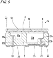
- FIG. 6 is a cross-sectional view of the measurement sensor 100 showing its structure.
- the measurement sensor 100 includes the measurement sensor package 1 or 1A, a light emitter 30, which is contained in a first recess 20a, and a light receiver 31, which is contained in a second recess 20b.
- the measurement sensor 100 is obtained by mounting the light emitter 30 and the light receiver 31 on the measurement sensor package 1 and connecting the light emitter 30 and the light receiver 31 to the connection pads 23a both using bonding wires 32, and joining the lid 3 to the substrate body 20.
- a VCSEL that can emit a laser beam with a wavelength of 850 nm may be used as the light emitter 30 for measuring blood flow using the optical Doppler effect.
- another device that emits a laser beam with a wavelength appropriate for the measurement object may be selected as the light emitter 30.
- any light receiver that can receive such a beam may be used as the light receiver 31.
- any light receiver that can receive such a beam with its wavelength changed may be used as the light receiver 31.
- connection pad 23a with, for example, the bonding wires 32 in the present embodiment
- the connection may be achieved with another method, such as flip chip connection, a method using bumps, or a method using an anisotropic conductive film.
- a signal output from the measurement sensor 100 is input to the arithmetic element, which can then calculate the blood flow rate based on, for example, the frequency of the illuminating light emitted from the light emitter 30 and the frequency of the scattered light received by the light receiver 31.
- the frame-shaped ground conductor layer 22 may be optional.
- the ground conductor layer 4 on the lid 3 and the ground via conductors 21 may be directly joined together for electrical connection between them.
- a measurement sensor package (using dielectric layers formed from alumina and being 3 mm long, 4.5 mm wide, 1.2 mm thick) having the same structure as the measurement sensor package 1 shown in Figs. 4 and 5 is prepared, and a vertical cavity surface emitting laser (VCSEL) with near-infrared wavelengths as the light emitter 30, and a silicon photodiode with a light receiving diameter of ⁇ 200 ⁇ m as the light receiver 31 are mounted on the measurement sensor package to obtain a measurement sensor according to an example of the present invention.
- VCSEL vertical cavity surface emitting laser
- a signal (power spectrum) output from the light emitter with no fingertip touching the lid 3 was measured.
- the method for measuring the power spectrum will be described.
- the output signal is a current generated when an object to be measured is illuminated with light emitted from the VCSEL and a photodiode receives the resultant diffused light.
- the output signal is extremely weak, and is amplified with an amplifier circuit.
- the resultant signal then undergoes analog-digital (AD) conversion.
- the resultant digital signal then undergoes Fourier transformation to determine the power spectrum.
- Figs. 7A and 7B are graphs showing the measurement results of power spectra in the example and the comparative example.
- Fig. 7A shows the results in the comparative example
- Fig. 7B shows the results in the example.
- the upper graph shows the results obtained without a fingertip touching the lid 3
- the lower graph shows the results obtained with a fingertip touching the lid.
- noise occurs at frequencies of about 9 to 10 kHz, and about 16 kHZ when a fingertip is touching the lid 3. No change is observed in the output at less than 2 kHz due to scattering by blood flow to be otherwise detected.
- Fig. 8 is a graph showing the evaluation results in the example and the comparative example.
- the maximum noise level was used as the evaluation results.
- the maximum noise level is calculated by subtracting the maximum output value and the minimum output value at frequencies greater than or equal to 2 kHz in the power spectrum. Noise is more notable as the maximum noise level increases, whereas less noise is generated as the minimum noise level is lower.
- the maximum noise level is small both in the example and the comparative example when a fingertip is not touching the lid 3. Additionally, the maximum noise level in the example is smaller than the maximum noise level in the comparative example, revealing that the structure of the example reduces even slight noise occurring when a fingertip is not touching the lid 3. When a fingertip is touching the lid 3, the maximum noise level increases only slightly in the example, whereas the maximum noise level increases in the comparative example as compared with when a fingertip is touching the lid 3.
- the structure of the example including the ground via conductors 21 reduces noise generated from a touch of an object to be measured, and enables highly accurate measurement of blood flow.
Claims (5)
- Boîtier de capteur de mesure (1, 1A), comprenant :un substrat (2) comprenant :un corps de substrat (20) comprenant une pluralité de couches diélectriques empilées les unes sur les autres, le corps de substrat (20) étant une plaque rectangulaire et comprenant un premier évidement (20a) et un second évidement (20b) sur une première surface de celui-ci, le premier évidement (20a) étant configuré pour contenir un émetteur de lumière (30), le second évidement (20b) étant configuré pour contenir un récepteur de lumière (31), etun ou plusieurs conducteurs d'interconnexion de masse (21) situés vers l'extérieur du premier évidement (20a) et du second évidement (20b) inclus dans le corps de substrat (20) dans une vue en plan, ledit ou lesdits plusieurs conducteurs d'interconnexion de masse (21) pouvant être connectés à un potentiel de masse,un couvercle (3) étant une plaque recouvrant le premier évidement (20a) et le second évidement (20b), le couvercle (3) comprenant un matériau isolant, le couvercle (3) étant configuré pour être mis en contact avec une partie du corps et étant configuré pour transmettre la lumière émise par l'émetteur de lumière (30) contenu dans le premier évidement (20a) et pour transmettre la lumière à recevoir par le récepteur de lumière (31) contenu dans le second évidement (20b), etune couche conductrice de masse (4) située sur une surface du couvercle (3) faisant face au premier évidement (20a) et au second évidement (20b) et pouvant être connectée à un potentiel de masse, la couche conductrice de masse (4) ayant une première ouverture (4a) configurée pour permettre un passage de la lumière émise par l'émetteur de lumière (30), et une seconde ouverture (4b) configurée pour permettre un passage de la lumière à recevoir par le récepteur de lumière (31), la couche conductrice de masse (4) pouvant être connectée électriquement audit un ou auxdits plusieurs conducteurs d'interconnexion de masse (21).
- Boîtier de capteur de mesure (1, 1A) selon la revendication 1, dans lequelledit un ou lesdits plusieurs conducteurs d'interconnexion de masse (21) comprennent une pluralité de conducteurs d'interconnexion de masse (21) inclus dans le substrat (2),la pluralité de conducteurs d'interconnexion de masse (21) est disposée le long d'un périmètre de la première surface du corps de substrat (20), et chacun de la pluralité de conducteurs d'interconnexion de masse (21) a une première face d'extrémité (21a) exposée sur la première surface du substrat (2), etle substrat (2) comprend une couche conductrice en forme de cadre (22) entourant une ouverture du premier évidement (20a) et une ouverture du second évidement (20b) sur la première surface du corps de substrat (20), et la couche conductrice en forme de cadre (22) est configurée pour être connectée électriquement à la première face d'extrémité (21a) de chacun de la pluralité de conducteurs d'interconnexion de masse (21).
- Boîtier de capteur de mesure (1, 1A) selon la revendication 1 ou la revendication 2, dans lequel le substrat (2) comprend une couche conductrice de masse interne (25) située entre un fond du second évidement (20b) et une seconde surface du corps de substrat (20) opposée à la première surface, et la couche conductrice de masse interne (25) peut être connectée à un potentiel de masse.
- Boîtier de capteur de mesure (1, 1A) selon l'une quelconque des revendications 1 à 3, dans lequel les couches diélectriques contiennent un matériau céramique.
- Capteur de mesure (100), comprenant :le boîtier de capteur de mesure (1, 1A) selon l'une quelconque des revendications 1 à 4 ;un émetteur de lumière (30) contenu dans le premier évidement ; etun récepteur de lumière (31) contenu dans le second évidement.
Priority Applications (1)
| Application Number | Priority Date | Filing Date | Title |
|---|---|---|---|
| EP21205560.2A EP4026493A1 (fr) | 2015-12-22 | 2016-11-10 | Module de capteur de mesure et capteur de mesure |
Applications Claiming Priority (2)
| Application Number | Priority Date | Filing Date | Title |
|---|---|---|---|
| JP2015250656 | 2015-12-22 | ||
| PCT/JP2016/083435 WO2017110291A1 (fr) | 2015-12-22 | 2016-11-10 | Module de capteur de mesure et capteur de mesure |
Related Child Applications (1)
| Application Number | Title | Priority Date | Filing Date |
|---|---|---|---|
| EP21205560.2A Division EP4026493A1 (fr) | 2015-12-22 | 2016-11-10 | Module de capteur de mesure et capteur de mesure |
Publications (3)
| Publication Number | Publication Date |
|---|---|
| EP3395242A1 EP3395242A1 (fr) | 2018-10-31 |
| EP3395242A4 EP3395242A4 (fr) | 2019-09-04 |
| EP3395242B1 true EP3395242B1 (fr) | 2021-11-10 |
Family
ID=59090416
Family Applications (2)
| Application Number | Title | Priority Date | Filing Date |
|---|---|---|---|
| EP16878189.6A Active EP3395242B1 (fr) | 2015-12-22 | 2016-11-10 | Module de capteur de mesure et capteur de mesure |
| EP21205560.2A Withdrawn EP4026493A1 (fr) | 2015-12-22 | 2016-11-10 | Module de capteur de mesure et capteur de mesure |
Family Applications After (1)
| Application Number | Title | Priority Date | Filing Date |
|---|---|---|---|
| EP21205560.2A Withdrawn EP4026493A1 (fr) | 2015-12-22 | 2016-11-10 | Module de capteur de mesure et capteur de mesure |
Country Status (6)
| Country | Link |
|---|---|
| US (1) | US11166642B2 (fr) |
| EP (2) | EP3395242B1 (fr) |
| JP (1) | JP6483859B2 (fr) |
| KR (1) | KR102136538B1 (fr) |
| CN (2) | CN108135516B (fr) |
| WO (1) | WO2017110291A1 (fr) |
Families Citing this family (3)
| Publication number | Priority date | Publication date | Assignee | Title |
|---|---|---|---|---|
| CN108351366A (zh) | 2016-01-25 | 2018-07-31 | 京瓷株式会社 | 测量传感器用封装体以及测量传感器 |
| US10582864B2 (en) * | 2016-04-04 | 2020-03-10 | Kyocera Corporation | Measurement sensor package and measurement sensor |
| JP7134246B2 (ja) * | 2018-10-30 | 2022-09-09 | 京セラ株式会社 | 光学センサ装置 |
Family Cites Families (25)
| Publication number | Priority date | Publication date | Assignee | Title |
|---|---|---|---|---|
| JPS5031895B1 (fr) | 1971-03-16 | 1975-10-16 | ||
| JPS5146596B2 (fr) * | 1972-09-06 | 1976-12-09 | ||
| JPH0712348B2 (ja) * | 1987-02-10 | 1995-02-15 | 松下電器産業株式会社 | 光電式脈波検出器 |
| US6300659B1 (en) * | 1994-09-30 | 2001-10-09 | Semiconductor Energy Laboratory Co., Ltd. | Thin-film transistor and fabrication method for same |
| KR100309957B1 (ko) * | 1997-09-08 | 2002-08-21 | 신꼬오덴기 고교 가부시키가이샤 | 반도체장치 |
| JP3554886B2 (ja) * | 2000-03-30 | 2004-08-18 | 日本特殊陶業株式会社 | 配線基板 |
| US6486534B1 (en) * | 2001-02-16 | 2002-11-26 | Ashvattha Semiconductor, Inc. | Integrated circuit die having an interference shield |
| JP2004041482A (ja) * | 2002-07-12 | 2004-02-12 | Seiko Epson Corp | 脈波検出装置及び生体電位検出装置 |
| JP2005260877A (ja) * | 2004-03-15 | 2005-09-22 | Kyocera Corp | 高周波モジュール及び無線通信装置 |
| JP4061409B2 (ja) * | 2004-11-09 | 2008-03-19 | 国立大学法人九州大学 | センサ部及び生体センサ |
| CN2879968Y (zh) * | 2006-02-17 | 2007-03-21 | 杭州大力神医疗器械有限公司 | 光电指脉传感器 |
| JP4708214B2 (ja) * | 2006-02-23 | 2011-06-22 | 浜松ホトニクス株式会社 | 光送受信デバイス |
| US20110260176A1 (en) * | 2008-05-12 | 2011-10-27 | Pioneer Corporation | Light-emitting sensor device and method for manufacturing the same |
| CN102026575B (zh) * | 2008-05-12 | 2013-12-18 | 日本先锋公司 | 自发光传感器装置 |
| JP5549104B2 (ja) * | 2008-05-29 | 2014-07-16 | 株式会社リコー | 発光装置、光走査装置及び画像形成装置 |
| US8577431B2 (en) * | 2008-07-03 | 2013-11-05 | Cercacor Laboratories, Inc. | Noise shielding for a noninvasive device |
| EP2425768B1 (fr) * | 2009-04-30 | 2015-02-25 | Murata Manufacturing Co., Ltd. | Dispositif biocapteur |
| JP2010264174A (ja) * | 2009-05-18 | 2010-11-25 | Hitachi Cable Ltd | 表面筋電位センサ |
| US8199518B1 (en) * | 2010-02-18 | 2012-06-12 | Amkor Technology, Inc. | Top feature package and method |
| US8258012B2 (en) * | 2010-05-14 | 2012-09-04 | Stats Chippac, Ltd. | Semiconductor device and method of forming discontinuous ESD protection layers between semiconductor die |
| US9490239B2 (en) * | 2011-08-31 | 2016-11-08 | Micron Technology, Inc. | Solid state transducers with state detection, and associated systems and methods |
| TWI453923B (zh) * | 2012-06-22 | 2014-09-21 | Txc Corp | Light sensing chip package structure |
| EP2931121B1 (fr) * | 2012-12-14 | 2017-02-22 | Koninklijke Philips N.V. | Dispositif pour mesurer un paramètre physiologique d'un utilisateur |
| EP2803315B1 (fr) * | 2013-05-15 | 2019-10-02 | Polar Electro Oy | Structure de capteur d'activité cardiaque |
| JP5907200B2 (ja) * | 2014-03-18 | 2016-04-26 | セイコーエプソン株式会社 | 光検出ユニット及び生体情報検出装置 |
-
2016
- 2016-11-10 US US15/770,658 patent/US11166642B2/en active Active
- 2016-11-10 CN CN201680060515.8A patent/CN108135516B/zh active Active
- 2016-11-10 EP EP16878189.6A patent/EP3395242B1/fr active Active
- 2016-11-10 KR KR1020187010706A patent/KR102136538B1/ko active IP Right Grant
- 2016-11-10 EP EP21205560.2A patent/EP4026493A1/fr not_active Withdrawn
- 2016-11-10 JP JP2017557785A patent/JP6483859B2/ja active Active
- 2016-11-10 CN CN202011206741.7A patent/CN112168146A/zh active Pending
- 2016-11-10 WO PCT/JP2016/083435 patent/WO2017110291A1/fr active Application Filing
Also Published As
| Publication number | Publication date |
|---|---|
| CN108135516A (zh) | 2018-06-08 |
| KR20180053383A (ko) | 2018-05-21 |
| EP4026493A1 (fr) | 2022-07-13 |
| EP3395242A1 (fr) | 2018-10-31 |
| CN108135516B (zh) | 2020-11-20 |
| US11166642B2 (en) | 2021-11-09 |
| JPWO2017110291A1 (ja) | 2018-08-16 |
| WO2017110291A1 (fr) | 2017-06-29 |
| JP6483859B2 (ja) | 2019-03-13 |
| KR102136538B1 (ko) | 2020-07-22 |
| US20180310836A1 (en) | 2018-11-01 |
| CN112168146A (zh) | 2021-01-05 |
| EP3395242A4 (fr) | 2019-09-04 |
Similar Documents
| Publication | Publication Date | Title |
|---|---|---|
| US10582864B2 (en) | Measurement sensor package and measurement sensor | |
| EP3395242B1 (fr) | Module de capteur de mesure et capteur de mesure | |
| JP6659377B2 (ja) | 計測センサ用パッケージおよび計測センサ | |
| US11717178B2 (en) | Measurement sensor package and measurement sensor | |
| JP6942211B2 (ja) | 計測センサ用パッケージおよび計測センサ | |
| JP6718339B2 (ja) | 計測センサ用パッケージおよび計測センサ | |
| JP6666191B2 (ja) | 計測センサ用パッケージおよび計測センサ | |
| JP2018196571A (ja) | 計測センサ用パッケージ及び計測センサ | |
| JP7267304B2 (ja) | 光学センサ装置 | |
| JP6666192B2 (ja) | 計測センサ用パッケージおよび計測センサ | |
| JP6753729B2 (ja) | 計測センサ用パッケージおよび計測センサ | |
| JP6753731B2 (ja) | 計測センサ用パッケージおよび計測センサ |
Legal Events
| Date | Code | Title | Description |
|---|---|---|---|
| STAA | Information on the status of an ep patent application or granted ep patent |
Free format text: STATUS: THE INTERNATIONAL PUBLICATION HAS BEEN MADE |
|
| PUAI | Public reference made under article 153(3) epc to a published international application that has entered the european phase |
Free format text: ORIGINAL CODE: 0009012 |
|
| STAA | Information on the status of an ep patent application or granted ep patent |
Free format text: STATUS: REQUEST FOR EXAMINATION WAS MADE |
|
| 17P | Request for examination filed |
Effective date: 20180425 |
|
| AK | Designated contracting states |
Kind code of ref document: A1 Designated state(s): AL AT BE BG CH CY CZ DE DK EE ES FI FR GB GR HR HU IE IS IT LI LT LU LV MC MK MT NL NO PL PT RO RS SE SI SK SM TR |
|
| AX | Request for extension of the european patent |
Extension state: BA ME |
|
| DAV | Request for validation of the european patent (deleted) | ||
| DAX | Request for extension of the european patent (deleted) | ||
| A4 | Supplementary search report drawn up and despatched |
Effective date: 20190801 |
|
| RIC1 | Information provided on ipc code assigned before grant |
Ipc: H05K 9/00 20060101ALI20190726BHEP Ipc: A61B 5/02 20060101ALI20190726BHEP Ipc: A61B 5/00 20060101ALI20190726BHEP Ipc: H01L 27/02 20060101ALI20190726BHEP Ipc: A61B 5/026 20060101AFI20190726BHEP |
|
| GRAP | Despatch of communication of intention to grant a patent |
Free format text: ORIGINAL CODE: EPIDOSNIGR1 |
|
| STAA | Information on the status of an ep patent application or granted ep patent |
Free format text: STATUS: GRANT OF PATENT IS INTENDED |
|
| INTG | Intention to grant announced |
Effective date: 20210531 |
|
| GRAS | Grant fee paid |
Free format text: ORIGINAL CODE: EPIDOSNIGR3 |
|
| GRAA | (expected) grant |
Free format text: ORIGINAL CODE: 0009210 |
|
| STAA | Information on the status of an ep patent application or granted ep patent |
Free format text: STATUS: THE PATENT HAS BEEN GRANTED |
|
| AK | Designated contracting states |
Kind code of ref document: B1 Designated state(s): AL AT BE BG CH CY CZ DE DK EE ES FI FR GB GR HR HU IE IS IT LI LT LU LV MC MK MT NL NO PL PT RO RS SE SI SK SM TR |
|
| REG | Reference to a national code |
Ref country code: GB Ref legal event code: FG4D |
|
| REG | Reference to a national code |
Ref country code: AT Ref legal event code: REF Ref document number: 1445317 Country of ref document: AT Kind code of ref document: T Effective date: 20211115 Ref country code: CH Ref legal event code: EP |
|
| REG | Reference to a national code |
Ref country code: DE Ref legal event code: R096 Ref document number: 602016066166 Country of ref document: DE |
|
| REG | Reference to a national code |
Ref country code: IE Ref legal event code: FG4D |
|
| REG | Reference to a national code |
Ref country code: LT Ref legal event code: MG9D |
|
| REG | Reference to a national code |
Ref country code: NL Ref legal event code: MP Effective date: 20211110 |
|
| REG | Reference to a national code |
Ref country code: AT Ref legal event code: MK05 Ref document number: 1445317 Country of ref document: AT Kind code of ref document: T Effective date: 20211110 |
|
| PG25 | Lapsed in a contracting state [announced via postgrant information from national office to epo] |
Ref country code: RS Free format text: LAPSE BECAUSE OF FAILURE TO SUBMIT A TRANSLATION OF THE DESCRIPTION OR TO PAY THE FEE WITHIN THE PRESCRIBED TIME-LIMIT Effective date: 20211110 Ref country code: LT Free format text: LAPSE BECAUSE OF FAILURE TO SUBMIT A TRANSLATION OF THE DESCRIPTION OR TO PAY THE FEE WITHIN THE PRESCRIBED TIME-LIMIT Effective date: 20211110 Ref country code: FI Free format text: LAPSE BECAUSE OF FAILURE TO SUBMIT A TRANSLATION OF THE DESCRIPTION OR TO PAY THE FEE WITHIN THE PRESCRIBED TIME-LIMIT Effective date: 20211110 Ref country code: BG Free format text: LAPSE BECAUSE OF FAILURE TO SUBMIT A TRANSLATION OF THE DESCRIPTION OR TO PAY THE FEE WITHIN THE PRESCRIBED TIME-LIMIT Effective date: 20220210 Ref country code: AT Free format text: LAPSE BECAUSE OF FAILURE TO SUBMIT A TRANSLATION OF THE DESCRIPTION OR TO PAY THE FEE WITHIN THE PRESCRIBED TIME-LIMIT Effective date: 20211110 |
|
| PG25 | Lapsed in a contracting state [announced via postgrant information from national office to epo] |
Ref country code: IS Free format text: LAPSE BECAUSE OF FAILURE TO SUBMIT A TRANSLATION OF THE DESCRIPTION OR TO PAY THE FEE WITHIN THE PRESCRIBED TIME-LIMIT Effective date: 20220310 Ref country code: SE Free format text: LAPSE BECAUSE OF FAILURE TO SUBMIT A TRANSLATION OF THE DESCRIPTION OR TO PAY THE FEE WITHIN THE PRESCRIBED TIME-LIMIT Effective date: 20211110 Ref country code: PT Free format text: LAPSE BECAUSE OF FAILURE TO SUBMIT A TRANSLATION OF THE DESCRIPTION OR TO PAY THE FEE WITHIN THE PRESCRIBED TIME-LIMIT Effective date: 20220310 Ref country code: PL Free format text: LAPSE BECAUSE OF FAILURE TO SUBMIT A TRANSLATION OF THE DESCRIPTION OR TO PAY THE FEE WITHIN THE PRESCRIBED TIME-LIMIT Effective date: 20211110 Ref country code: NO Free format text: LAPSE BECAUSE OF FAILURE TO SUBMIT A TRANSLATION OF THE DESCRIPTION OR TO PAY THE FEE WITHIN THE PRESCRIBED TIME-LIMIT Effective date: 20220210 Ref country code: NL Free format text: LAPSE BECAUSE OF FAILURE TO SUBMIT A TRANSLATION OF THE DESCRIPTION OR TO PAY THE FEE WITHIN THE PRESCRIBED TIME-LIMIT Effective date: 20211110 Ref country code: LV Free format text: LAPSE BECAUSE OF FAILURE TO SUBMIT A TRANSLATION OF THE DESCRIPTION OR TO PAY THE FEE WITHIN THE PRESCRIBED TIME-LIMIT Effective date: 20211110 Ref country code: HR Free format text: LAPSE BECAUSE OF FAILURE TO SUBMIT A TRANSLATION OF THE DESCRIPTION OR TO PAY THE FEE WITHIN THE PRESCRIBED TIME-LIMIT Effective date: 20211110 Ref country code: GR Free format text: LAPSE BECAUSE OF FAILURE TO SUBMIT A TRANSLATION OF THE DESCRIPTION OR TO PAY THE FEE WITHIN THE PRESCRIBED TIME-LIMIT Effective date: 20220211 Ref country code: ES Free format text: LAPSE BECAUSE OF FAILURE TO SUBMIT A TRANSLATION OF THE DESCRIPTION OR TO PAY THE FEE WITHIN THE PRESCRIBED TIME-LIMIT Effective date: 20211110 |
|
| REG | Reference to a national code |
Ref country code: CH Ref legal event code: PL |
|
| PG25 | Lapsed in a contracting state [announced via postgrant information from national office to epo] |
Ref country code: SM Free format text: LAPSE BECAUSE OF FAILURE TO SUBMIT A TRANSLATION OF THE DESCRIPTION OR TO PAY THE FEE WITHIN THE PRESCRIBED TIME-LIMIT Effective date: 20211110 Ref country code: SK Free format text: LAPSE BECAUSE OF FAILURE TO SUBMIT A TRANSLATION OF THE DESCRIPTION OR TO PAY THE FEE WITHIN THE PRESCRIBED TIME-LIMIT Effective date: 20211110 Ref country code: RO Free format text: LAPSE BECAUSE OF FAILURE TO SUBMIT A TRANSLATION OF THE DESCRIPTION OR TO PAY THE FEE WITHIN THE PRESCRIBED TIME-LIMIT Effective date: 20211110 Ref country code: LU Free format text: LAPSE BECAUSE OF NON-PAYMENT OF DUE FEES Effective date: 20211110 Ref country code: EE Free format text: LAPSE BECAUSE OF FAILURE TO SUBMIT A TRANSLATION OF THE DESCRIPTION OR TO PAY THE FEE WITHIN THE PRESCRIBED TIME-LIMIT Effective date: 20211110 Ref country code: DK Free format text: LAPSE BECAUSE OF FAILURE TO SUBMIT A TRANSLATION OF THE DESCRIPTION OR TO PAY THE FEE WITHIN THE PRESCRIBED TIME-LIMIT Effective date: 20211110 Ref country code: CZ Free format text: LAPSE BECAUSE OF FAILURE TO SUBMIT A TRANSLATION OF THE DESCRIPTION OR TO PAY THE FEE WITHIN THE PRESCRIBED TIME-LIMIT Effective date: 20211110 Ref country code: BE Free format text: LAPSE BECAUSE OF NON-PAYMENT OF DUE FEES Effective date: 20211130 |
|
| REG | Reference to a national code |
Ref country code: BE Ref legal event code: MM Effective date: 20211130 |
|
| REG | Reference to a national code |
Ref country code: DE Ref legal event code: R097 Ref document number: 602016066166 Country of ref document: DE |
|
| PG25 | Lapsed in a contracting state [announced via postgrant information from national office to epo] |
Ref country code: MC Free format text: LAPSE BECAUSE OF FAILURE TO SUBMIT A TRANSLATION OF THE DESCRIPTION OR TO PAY THE FEE WITHIN THE PRESCRIBED TIME-LIMIT Effective date: 20211110 Ref country code: LI Free format text: LAPSE BECAUSE OF NON-PAYMENT OF DUE FEES Effective date: 20211130 Ref country code: CH Free format text: LAPSE BECAUSE OF NON-PAYMENT OF DUE FEES Effective date: 20211130 |
|
| PLBE | No opposition filed within time limit |
Free format text: ORIGINAL CODE: 0009261 |
|
| STAA | Information on the status of an ep patent application or granted ep patent |
Free format text: STATUS: NO OPPOSITION FILED WITHIN TIME LIMIT |
|
| 26N | No opposition filed |
Effective date: 20220811 |
|
| GBPC | Gb: european patent ceased through non-payment of renewal fee |
Effective date: 20220210 |
|
| PG25 | Lapsed in a contracting state [announced via postgrant information from national office to epo] |
Ref country code: IE Free format text: LAPSE BECAUSE OF NON-PAYMENT OF DUE FEES Effective date: 20211110 Ref country code: AL Free format text: LAPSE BECAUSE OF FAILURE TO SUBMIT A TRANSLATION OF THE DESCRIPTION OR TO PAY THE FEE WITHIN THE PRESCRIBED TIME-LIMIT Effective date: 20211110 |
|
| PG25 | Lapsed in a contracting state [announced via postgrant information from national office to epo] |
Ref country code: SI Free format text: LAPSE BECAUSE OF FAILURE TO SUBMIT A TRANSLATION OF THE DESCRIPTION OR TO PAY THE FEE WITHIN THE PRESCRIBED TIME-LIMIT Effective date: 20211110 |
|
| PG25 | Lapsed in a contracting state [announced via postgrant information from national office to epo] |
Ref country code: GB Free format text: LAPSE BECAUSE OF NON-PAYMENT OF DUE FEES Effective date: 20220210 |
|
| PG25 | Lapsed in a contracting state [announced via postgrant information from national office to epo] |
Ref country code: IT Free format text: LAPSE BECAUSE OF FAILURE TO SUBMIT A TRANSLATION OF THE DESCRIPTION OR TO PAY THE FEE WITHIN THE PRESCRIBED TIME-LIMIT Effective date: 20211110 |
|
| P01 | Opt-out of the competence of the unified patent court (upc) registered |
Effective date: 20230505 |
|
| PG25 | Lapsed in a contracting state [announced via postgrant information from national office to epo] |
Ref country code: CY Free format text: LAPSE BECAUSE OF FAILURE TO SUBMIT A TRANSLATION OF THE DESCRIPTION OR TO PAY THE FEE WITHIN THE PRESCRIBED TIME-LIMIT Effective date: 20211110 |
|
| PG25 | Lapsed in a contracting state [announced via postgrant information from national office to epo] |
Ref country code: HU Free format text: LAPSE BECAUSE OF FAILURE TO SUBMIT A TRANSLATION OF THE DESCRIPTION OR TO PAY THE FEE WITHIN THE PRESCRIBED TIME-LIMIT; INVALID AB INITIO Effective date: 20161110 |
|
| PGFP | Annual fee paid to national office [announced via postgrant information from national office to epo] |
Ref country code: FR Payment date: 20231009 Year of fee payment: 8 Ref country code: DE Payment date: 20231003 Year of fee payment: 8 |