EP3389151B1 - Wechselstrommotorsteuergerät, laminierte stromschienenanordnung und herstellungsverfahren dafür - Google Patents
Wechselstrommotorsteuergerät, laminierte stromschienenanordnung und herstellungsverfahren dafür Download PDFInfo
- Publication number
- EP3389151B1 EP3389151B1 EP17781823.4A EP17781823A EP3389151B1 EP 3389151 B1 EP3389151 B1 EP 3389151B1 EP 17781823 A EP17781823 A EP 17781823A EP 3389151 B1 EP3389151 B1 EP 3389151B1
- Authority
- EP
- European Patent Office
- Prior art keywords
- pin
- metal plate
- plate
- substrate
- connecting part
- Prior art date
- Legal status (The legal status is an assumption and is not a legal conclusion. Google has not performed a legal analysis and makes no representation as to the accuracy of the status listed.)
- Active
Links
Images



Classifications
-
- H—ELECTRICITY
- H01—ELECTRIC ELEMENTS
- H01R—ELECTRICALLY-CONDUCTIVE CONNECTIONS; STRUCTURAL ASSOCIATIONS OF A PLURALITY OF MUTUALLY-INSULATED ELECTRICAL CONNECTING ELEMENTS; COUPLING DEVICES; CURRENT COLLECTORS
- H01R25/00—Coupling parts adapted for simultaneous co-operation with two or more identical counterparts, e.g. for distributing energy to two or more circuits
- H01R25/16—Rails or bus-bars provided with a plurality of discrete connecting locations for counterparts
- H01R25/161—Details
- H01R25/162—Electrical connections between or with rails or bus-bars
-
- H—ELECTRICITY
- H05—ELECTRIC TECHNIQUES NOT OTHERWISE PROVIDED FOR
- H05K—PRINTED CIRCUITS; CASINGS OR CONSTRUCTIONAL DETAILS OF ELECTRIC APPARATUS; MANUFACTURE OF ASSEMBLAGES OF ELECTRICAL COMPONENTS
- H05K1/00—Printed circuits
- H05K1/02—Details
- H05K1/0213—Electrical arrangements not otherwise provided for
- H05K1/0263—High current adaptations, e.g. printed high current conductors or using auxiliary non-printed means; Fine and coarse circuit patterns on one circuit board
-
- H—ELECTRICITY
- H01—ELECTRIC ELEMENTS
- H01R—ELECTRICALLY-CONDUCTIVE CONNECTIONS; STRUCTURAL ASSOCIATIONS OF A PLURALITY OF MUTUALLY-INSULATED ELECTRICAL CONNECTING ELEMENTS; COUPLING DEVICES; CURRENT COLLECTORS
- H01R25/00—Coupling parts adapted for simultaneous co-operation with two or more identical counterparts, e.g. for distributing energy to two or more circuits
- H01R25/16—Rails or bus-bars provided with a plurality of discrete connecting locations for counterparts
-
- H—ELECTRICITY
- H01—ELECTRIC ELEMENTS
- H01R—ELECTRICALLY-CONDUCTIVE CONNECTIONS; STRUCTURAL ASSOCIATIONS OF A PLURALITY OF MUTUALLY-INSULATED ELECTRICAL CONNECTING ELEMENTS; COUPLING DEVICES; CURRENT COLLECTORS
- H01R43/00—Apparatus or processes specially adapted for manufacturing, assembling, maintaining, or repairing of line connectors or current collectors or for joining electric conductors
- H01R43/18—Apparatus or processes specially adapted for manufacturing, assembling, maintaining, or repairing of line connectors or current collectors or for joining electric conductors for manufacturing bases or cases for contact members
-
- H—ELECTRICITY
- H02—GENERATION; CONVERSION OR DISTRIBUTION OF ELECTRIC POWER
- H02B—BOARDS, SUBSTATIONS OR SWITCHING ARRANGEMENTS FOR THE SUPPLY OR DISTRIBUTION OF ELECTRIC POWER
- H02B1/00—Frameworks, boards, panels, desks, casings; Details of substations or switching arrangements
- H02B1/20—Bus-bar or other wiring layouts, e.g. in cubicles, in switchyards
- H02B1/205—Bus-bar or other wiring layouts, e.g. in cubicles, in switchyards for connecting electrical apparatus mounted side by side on a rail
-
- H—ELECTRICITY
- H02—GENERATION; CONVERSION OR DISTRIBUTION OF ELECTRIC POWER
- H02M—APPARATUS FOR CONVERSION BETWEEN AC AND AC, BETWEEN AC AND DC, OR BETWEEN DC AND DC, AND FOR USE WITH MAINS OR SIMILAR POWER SUPPLY SYSTEMS; CONVERSION OF DC OR AC INPUT POWER INTO SURGE OUTPUT POWER; CONTROL OR REGULATION THEREOF
- H02M7/00—Conversion of AC power input into DC power output; Conversion of DC power input into AC power output
- H02M7/003—Constructional details, e.g. physical layout, assembly, wiring or busbar connections
-
- H—ELECTRICITY
- H02—GENERATION; CONVERSION OR DISTRIBUTION OF ELECTRIC POWER
- H02P—CONTROL OR REGULATION OF ELECTRIC MOTORS, ELECTRIC GENERATORS OR DYNAMO-ELECTRIC CONVERTERS; CONTROLLING TRANSFORMERS, REACTORS OR CHOKE COILS
- H02P23/00—Arrangements or methods for the control of AC motors characterised by a control method other than vector control
-
- H—ELECTRICITY
- H01—ELECTRIC ELEMENTS
- H01R—ELECTRICALLY-CONDUCTIVE CONNECTIONS; STRUCTURAL ASSOCIATIONS OF A PLURALITY OF MUTUALLY-INSULATED ELECTRICAL CONNECTING ELEMENTS; COUPLING DEVICES; CURRENT COLLECTORS
- H01R2201/00—Connectors or connections adapted for particular applications
- H01R2201/10—Connectors or connections adapted for particular applications for dynamoelectric machines
-
- H—ELECTRICITY
- H05—ELECTRIC TECHNIQUES NOT OTHERWISE PROVIDED FOR
- H05K—PRINTED CIRCUITS; CASINGS OR CONSTRUCTIONAL DETAILS OF ELECTRIC APPARATUS; MANUFACTURE OF ASSEMBLAGES OF ELECTRICAL COMPONENTS
- H05K2201/00—Indexing scheme relating to printed circuits covered by H05K1/00
- H05K2201/10—Details of components or other objects attached to or integrated in a printed circuit board
- H05K2201/10007—Types of components
- H05K2201/10015—Non-printed capacitor
-
- H—ELECTRICITY
- H05—ELECTRIC TECHNIQUES NOT OTHERWISE PROVIDED FOR
- H05K—PRINTED CIRCUITS; CASINGS OR CONSTRUCTIONAL DETAILS OF ELECTRIC APPARATUS; MANUFACTURE OF ASSEMBLAGES OF ELECTRICAL COMPONENTS
- H05K2201/00—Indexing scheme relating to printed circuits covered by H05K1/00
- H05K2201/10—Details of components or other objects attached to or integrated in a printed circuit board
- H05K2201/10007—Types of components
- H05K2201/10166—Transistor
-
- H—ELECTRICITY
- H05—ELECTRIC TECHNIQUES NOT OTHERWISE PROVIDED FOR
- H05K—PRINTED CIRCUITS; CASINGS OR CONSTRUCTIONAL DETAILS OF ELECTRIC APPARATUS; MANUFACTURE OF ASSEMBLAGES OF ELECTRICAL COMPONENTS
- H05K3/00—Apparatus or processes for manufacturing printed circuits
- H05K3/30—Assembling printed circuits with electric components, e.g. with resistors
- H05K3/32—Assembling printed circuits with electric components, e.g. with resistors electrically connecting electric components or wires to printed circuits
- H05K3/34—Assembling printed circuits with electric components, e.g. with resistors electrically connecting electric components or wires to printed circuits by soldering
- H05K3/3447—Lead-in-hole components
Definitions
- the present invention relates to the field of the electrical components, in particular to an alternating current (AC) motor controller and a laminated busbar assembly used in the battery operated electric vehicles, and manufacturing method of the laminated busbar assembly.
- AC alternating current
- the present application is based upon Chinese utility patent application No. CN201610223280.1 filed on April 11, 2016 .
- the battery operated electric vehicles have been widely used in the places with high environmental requirements such as tourist attractions etc. because they derive power without burning gasoline, and thus are environment friendly and cause low-pollution.
- Currently available battery operated electric vehicles are provided with an AC motor controller which is used to convert the direct current (DC) power output from the storage battery into three-phase AC power and drive the motor.
- DC direct current
- the printed circuit board is indispensable and widely used in the electric field.
- the substrate is provided with some built-in wirings, and pad hole groups are arranged on the wirings. Different electronic elements are arranged and soldered to the pad holes to form various kinds of PCBs for different uses.
- the AC motor controller is used to convert the DC power output from the storage battery into three-phase AC power and drive the motor.
- An AC motor controller in the prior art includes a substrate.
- the substrate is provided with a first DC power supply terminal, a second DC power supply terminal, and a current output terminal.
- a plurality of first controllable switching elements are connected between the first DC power supply terminal and the current output terminal.
- a plurality of second controllable switching elements are connected between the current output terminal and the second DC power supply terminal.
- Other circuit elements of the circuit may also be arranged on the substrate according to the requirements of power supply.
- the first DC power supply terminal, the second DC power supply terminal, the current output terminal, and the substrate are electrically connected with each other by configuring copper-pour blocks.
- the first controllable switching element, the second controllable switching element, and the circuit elements of the circuit are electrically connected to the substrate by plugging in one by one and tin soldering while the IGBT is fixed to the substrate by bolts.
- US patent US6283769 discloses an electric connecting box which is provided that has excellent connecting reliability between a printed circuit board and a bus-bar laminated body.
- the electric connecting box includes a bus-bar laminated body including a bus-bar and an insulating base material, a printed circuit board electrically connected therewith, and a connecting block.
- the connecting block is configured to hold connecting terminals by partially molding a plurality of connecting terminals in a resin insulator block.
- the first end of each connecting terminal protrudes from the resin insulator block and is soldered with a conductor on one side of the printed circuit board.
- the second end of each connecting terminal is fixed to a connecting area on a side of the bus-bar laminated body.
- US patent US6538878 discloses a bus bar assembly which comprising a high power transistor module directly mounted to a bus bar.
- the bus bar has the improved solderabilty of the results by forming a soldering island in the bus bar at predetermined points thereof.
- the soldering island comprises a central soldering opening, which receives the soldering pin, and a plurality of thermal barrier openings distributed around the soldering opening.
- the first purpose of the present invention is to provide a laminated busbar assembly with high production efficiency, good expansibility, and wide application.
- the second purpose of the present invention is to provide an AC motor controller with high degree of modularization and high production efficiency.
- the third purpose of the present invention is to provide a manufacturing method of the laminated busbar assembly with high production efficiency.
- the present invention provides a laminated busbar assembly according to claim 1.
- the laminated busbar assembly also includes an avoiding hole group.
- the avoiding hole group is arranged on the each of the positive metal plate, the negative metal plate, the output current metal plate, and the insulation layer group.
- the first pin, the second pin, and the third pin pass through the avoiding hole group.
- the laminated busbar assembly also includes an insulation plate.
- the insulation plate, the substrate, the positive metal plate, the negative metal plate, the output current metal plate, and the insulation layer group are arranged in a laminated manner.
- the insulation plate is located at the outermost end away from the substrate.
- the avoiding hole group is also configured on the insulation plate.
- first pin, the second pin, and the third pin are configured on one side of the avoiding hole group.
- the laminated busbar assembly also includes a positive bus plate.
- the positive bus plate is provided with a fourth pin.
- the fourth pin passes through the first pad hole and adjoins the first connecting part.
- the laminated busbar assembly also includes a negative bus plate.
- the negative bus plate is provided with a fifth pin.
- the fifth pin passes through the second pad hole and adjoins the second connecting part.
- the laminated busbar assembly also includes an output bus plate.
- the output bus plate is provided with a sixth pin.
- the sixth pin passes through the third pad hole and adjoins the third connecting part.
- first pin and the first pad hole are configured in an interference fit.
- the second pin and the second pad hole are configured in an interference fit.
- the third pin and the third pad hole are configured in an interference fit.
- the positive bus plate is provided with first protrusion portions between the fourth pins.
- the negative bus plate is provided with second protrusion portions between the fifth pins.
- the output bus plate is provided with third protrusion portions between the sixth pins.
- the present invention provides an AC motor controller which includes a laminated busbar assembly, a controllable switching element assembly, and a filter element assembly.
- the laminated busbar assembly includes a substrate which is provided with a pad hole group.
- a pad hole group is electrically connected to copper pour in the substrate to form the wirings.
- the pad hole group includes a first pad hole, a second pad hole, and a third pad hole, characterized in that the positive metal plate is provided with a first pin.
- the positive metal plate is arranged on a first side of the substrate.
- the first pin passes through the first pad hole.
- a first connecting part is configured at the second side of the substrate by the first pin.
- the negative metal plate is provided with a second pin.
- the negative metal plate is arranged on the first side of the substrate.
- the second pin passes through the second pad hole.
- a second connecting part is configured as the second side of the substrate by the second pin.
- the output current metal plate is provided with a third pin.
- the output current metal plate is arranged on the first side of the substrate.
- the third pin passes through the third pad hole.
- a third connecting part is configured at the second side of the substrate by the third pin.
- the substrate, the positive metal plate, the negative metal plate, and the output current metal plate are arranged in a laminated manner.
- the first connecting part is connected to the third connecting part.
- the second connecting part is connected to the third connecting part.
- the first connecting part is connected to the second connecting part.
- a controllable switching element assembly is connected between the first connecting part and the third connecting part.
- a controllable switching element assembly is connected between the second connecting part and the third connecting part.
- the filter element assembly is connected between the first connecting part and the second connecting part.
- the present invention provides a manufacturing method of the laminated busbar assembly which includes a substrate, a positive metal plate, a negative metal plate, and an output current metal plate.
- the substrate is provided with a pad hole group.
- the pad hole group is electrically connected to copper pour in the substrate to form the wirings.
- the pad hole group includes a first pad hole, a second pad hole, and a third pad hole.
- the positive metal plate is provided with a first pin.
- the positive metal plate is arranged on a first side of the substrate.
- the first pin passes through the first pad hole.
- a first connecting part is configured at the second side of the substrate by the first pin.
- the negative metal plate is provided with a second pin.
- the negative metal plate is arranged on the first side of the substrate.
- the second pin passes through the second pad hole.
- a second connecting part is configured at the second side of the substrate and is provided with corresponding to the second pin.
- the output current metal plate is provided with a third pin.
- the output current metal plate is arranged on the first side of the substrate.
- the third pin passes through the third pad hole.
- a third connecting part is configured at the second side of the substrate by the third pin.
- the substrate, the positive metal plate, the negative metal plate, and the output current metal plate are arranged in a laminated manner.
- the first connecting part is connected to the third connecting part.
- the second connecting part is connected to the third connecting part.
- the first connecting part is connected to the second connecting part.
- the present invention is characterized in that the manufacturing method of the laminated busbar assembly includes: a positive metal plate laminated on the substrate, wherein the first pin is inserted into the first pad hole; a negative metal plate laminated on the positive metal plate, wherein the second pin is inserted into the second pad hole; the output current metal plate laminated on the negative metal plate, wherein the third pin is inserted into the third pad hole.
- the reflow soldering is simultaneously performed between the first pin and the first pad hole, the second pin and the second pad hole, the third pin and the third pad hole.
- the present invention provides an AC motor controller, a laminated busbar assembly and a manufacturing method thereof.
- the first pin of the positive metal plate, the second pin of the negative metal plate, and the third pin of the output current metal plate pass through the pad hole group on the substrate from the same side.
- the second side of the substrate is provided with a first connecting part, a second connecting part, and a third connecting part, respectively.
- the substrate, the positive metal plate, the negative metal plate, and the output current metal plate are arranged in a laminated manner.
- the assembly process of the electronic control device based on the laminated busbar assembly a plurality of different circuit elements of the circuit, the positive metal plates, the negative metal plates, and the output current metal plates can be laminated and compressed at the same time, and respective preset pin can pass through the respective preset pad hole group of the substrate at the same time, then the assembly and soldering of electronic control device based on laminated busbar assembly can be completed by a one-off reflow soldering process.
- the laminated busbar not only can provide a network with large current, but also can be mass produced using automation equipment, thereby greatly improving the production efficiency, and a strong expansibility and wide use can be realized.
- the insulation layer group may be a separate insulation piece or an insulation coating covering on the substrate, positive metal plate, negative metal plate, or output current metal plate. Because the substrate, the positive metal plate, the negative metal plate, and the output current metal plate all have electrical conductivity, the breakdown by current and short out of circuit between adjacent plates can be effectively avoided by providing the insulation layer group on one side of each of the substrate, the positive metal plate, the negative metal plate, and the output current metal plate. Meanwhile, the external elements of circuit element can be prevented from breakdown and short circuit, thereby protecting the circuit. Moreover, the intervals of plates do not need to be controlled in the compressing process, thereby improving the production efficiency.
- the avoiding hole group by configuring the avoiding hole group, the first pin, the second pin, or the third pin directly passes through the positive metal plate, the negative metal plate, or the output current metal plate before passing through the substrate without detour, so that the wiring of circuit is more convenient.
- the avoiding hole has a function of positioning the pin in a sense, thereby improving the stability in the process of assembling and compressing and the yield, effectively.
- the insulation plate can prevent the external circuit element, the positive metal plate, the negative metal plate, and the output current metal plate from being broken down and shorted out, thus avoiding damages to the circuit, and the insulation plate has a pressure-proof and protection function for the laminated busbar assembly.
- the pins of the external circuit element can pass through the avoiding hole group of the insulation plate directly, then pass through the avoiding hole groups of the positive metal plate, the negative metal plate, the output current metal plate, and the insulation layer group, and finally pass through the pad hole group of the substrate to form the connection of circuit.
- the holes of positive metal plate are formed hole through the process of stamping or milling, drilling and so on.
- the protrusion portion of the edge contour of the hole extends toward the hole.
- the first pin is formed by bending the protrusion portion of the edge contour.
- the holes are directly configured as avoiding holes, so another trepanning process is not needed and the production efficiency is effectively improved.
- the positive bus plate and the negative bus plate serve as the current input terminal.
- the output bus plate serves as the current output terminal.
- the positive bus plate, the negative bus plate, and the output bus plate can pass through the pad hole to proceed tin soldering with the substrate. That is to say, when the lamination, compressing, and installation of the laminated busbar assembly are performed, the positive bus plate, the negative bus plate, and the output bus plate can be laminated and compressed concurrently, so the process is optimized and the efficiency is improved.
- the positions among the plates are relatively fixed after the compressing and assembling process, and the relative position between the first pin, the second pin, the third pin and the pad hole group is also fixed, so the processing efficiency of the tin soldering in the subsequent step, the stability, and the yield are improved.
- the positive bus plate as an example, when the fourth pin of the positive bus plate is in interference fit with the pad hole group of the substrate, each of the metal plates between the positive bus plate and the substrate are compressed and fixed by the first protrusion portion, so the structure of the laminated busbar assembly is more compact and stable, and the occurrence of rosin joint can be avoided.
- first pin of the positive metal plate, the second pin of the negative metal plate, and the third pin of the output current metal plate pass through the pad hole group of the substrate from the same side, and form the first connecting part, the second connecting part, and the third connecting part, respectively.
- the substrate, the positive metal plate, the negative metal plate, and the output current metal plate are arranged in a laminated manner.
- the laminated busbar assembly has a strong expansibility, greatly improves the production efficiency, and is widely used.
- the manufacturing steps are greatly reduced compared with the manufacturing steps of the busbar available now, so the production efficiency is greatly improved and the laminated busbar assembly can be widely used.
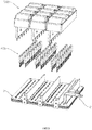
- FIG. 1 shows a structural view of an AC motor controller.
- the AC motor controller includes a laminated busbar assembly 1, an input bus plate 2, an output bus plate 3, and a circuit element 4.
- the function of the AC motor controller is to convert the DC current input into an AC output through a controllable switching element such as power transistor, so as to supply power to the drive motor.
- the difference between the laminated busbar assembly 1 of the embodiment and the existing busbar is that the laminated busbar assembly is formed by laminating multiple layers of metal plates, the pins of respective metal plate pass through avoiding holes of another metal plate and finally reach the position of a pad hole group of the substrate.
- FIG. 2 shows a structural view from another angle of the AC motor controller.
- the circuit element 4 includes a combined power transistor module 400 and a capacitor array 500.
- the combined power transistor module 400 is a controllable switching element module.
- the capacitor array 500 is a filter element module. After the laminated busbar assembly 1 is assembled, the corresponding pins of the combined power transistor module 400 and the corresponding pins of the capacitor array 500 may pass through the avoiding hole group of the laminated busbar assembly 1, and eventually pass through the pad hole group of the substrate to realize the connections of the circuit.
- the corresponding hard parts of the input bus plate 2 and the output bus plate 3 pass through the avoiding holes of the laminated busbar assembly 1 and reach the pad hole group of the substrate to realize the connections of the circuit.
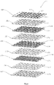
- FIG. 4 is an exploded view showing the structure of the laminated busbar assembly.
- the substrate 110 is the base of the laminated busbar assembly.
- Pad hole groups are arranged on the substrate 110.
- the pad hole groups are connected to each other through copper pour in the substrate to form electrical connection of the circuit.
- the pad hole groups include a plurality of first pad holes 111, a plurality of second pad holes 112, and a plurality of third pad holes 113.
- the plurality of first pad holes 111, the plurality of second pad holes 112, and the plurality of third pad holes 113 are evenly and straightly arranged on the substrate 110, so it is easy to position a plurality of modularized elements or the pins of the current bus plate in the insertion, and more positions are provided for elements to be soldered.
- first insulation piece 151, positive metal plate 120, second insulation piece 152, negative metal plate 130, third insulation piece 153, output current metal plate 140, fourth insulation piece 154, and insulation plate 160 is successively laminated with first insulation piece 151, positive metal plate 120, second insulation piece 152, negative metal plate 130, third insulation piece 153, output current metal plate 140, fourth insulation piece 154, and insulation plate 160.
- first insulation piece 151, the second insulation piece 152, third insulation piece 153, and fourth insulation piece 154 forms the insulation layer group of the present embodiment.
- the insulation layer group, the positive metal plate 120, the negative metal plate 130, the output current metal plate 140, and the insulation plate 160 are correspondingly provided with a plurality of avoiding holes.
- the insulation layer group may also be an insulation clad layer plated on the positive metal plate 120, the negative metal plate 130, and/or the output current metal plate 140.
- a plurality of first pins 121 are arranged on the positive metal plate 120.
- the plurality of first pins 121 are arranged perpendicular to the positive metal plate 120.All of the first pins 121 respectively pass through first avoiding hole 171 of the first insulation piece 151 above them, and then continue to pass through the first pad hole 111 of the substrate 110. After the first pins 121 pass through the first pad holes 111 and reach the second side of the substrate 110, a first connecting part is configured at the second side of the substrate by the first pin 121.
- a plurality of second pins 131 are arranged on the negative metal plate 130 and are perpendicularly upward to the negative metal plate 130.All of the second pins 131 successively pass through third avoiding holes 173 of second insulation piece 152, second avoiding holes 172 of the positive metal plate 120, and first avoiding holes 171 of the first insulation piece 151 above the second pins, and finally pass through the second pad holes 112 of the substrate 110.
- the second pin 131 passes through the second pad hole 112 and reaches the second side of the substrate 110.
- a second connecting part is configured at the second side of the substrate by the second pin 131.
- a plurality of third pins 141 are arranged on the output current metal plate 140 and perpendicularly upward to the output current metal plate 140. All of the third pins 141 successively pass through the fifth avoiding holes 175 of the third insulation piece 153,the fourth avoiding holes 174 of the negative metal plate 130, the third avoiding holes 173 of the second insulation piece 152, the second avoiding holes 172 of the positive metal plate 120,the first avoiding holes 171 of the first insulation piece 151 above the third pins 141,and finally pass through the third pad holes 113 of the substrate 110.
- the third pin 141 passes through the third pad hole 113 and reach the second side of the substrate 110.
- a third connecting part is configured at the second side of the substrate by the third pin 141.
- Pieces made of insulation materials are arranged between the positive metal plate 120, the negative metal plate 130, and the output current metal plate 140, so pairwise electrical conduction among them which may destroy the arrangement of the circuit can be prevented.
- the first connecting part of the first pin 121, the second connecting part of the second pin 131, and the third connecting part of the third pin 141 may be connected to each other through an intermediate substance such as a power transistor, a capacitor etc.
- the fourth insulation piece 154 and the insulation plate 160 are successively arranged below the output current metal plate 140. Seventh avoiding holes 177 are arranged on the fourth insulation piece 154.Eighth avoiding holes 178 are arranged on the insulation plate 160.
- the power transistor element and the filter capacitor etc. may be arranged at the lower side of the insulation plate 160. The pins of the power transistor element and the filter capacitor element may pass through the avoiding hole group and finally reach the pad hole group of the substrate 110 to be electrically connected to the first connecting part of the first pin 121, the second connecting part of the second pin 131, or third connecting part of third pin 141.
- the pins of the metal plate are arranged on a side of the corresponding avoiding holes.
- the processing procedure of first pin 121 is as follows. First, a machine tool is used to perform the process of material removing, such as a stamping process or a milling, drilling process etc. so as to form a through hole on the positive metal plate 120. The edge of the through hole is partially same as the contour of the first pin 121. Then the edge of the contour is bent to protrude from the positive metal plate to form the first pin 121. If the contour of the second avoiding hole 172 is generated while the contour of the first pin 121 is processed in the material removing procedure, the additional processing procedure of the avoiding hole may be saved.
- FIG. 5 is an exploded view showing the structure of the components of the AC motor controller excluding laminated busbar assembly 1.
- the input bus plate 2 includes a positive bus plate 210 and a negative bus plate 220.
- a metal copper busbar may be used as the bus plate.
- An upper part of the positive bus plate 210 is provided with fourth pins 211 aligned in a row.
- a lower part of the positive bus plate 210 is provided with a positive input terminal 212.
- An upper part of the negative bus plate 220 is provided with fifth pins 221 aligned in a row.
- the lower part of the negative bus plate 220 is provided with a negative input terminal 222.
- the positive input terminal 212 and the negative input terminal 222 are the input terminals of direct current (DC).
- the input terminal is electrically connected to the battery and receives power from the battery.
- the output bus plate 3 includes U-phase output bus plate 310, V-phase output bus plate 320, and W-phase output bus plate 330.
- the sixth pin 301 of the output bus plate 3 includes U-phase sixth pin 311, V-phase sixth pin 321 and W-phase sixth pin 331.
- a first protrusion portion 213 is arranged between every adjacent fourth pins 211 on the positive bus plate 210.
- a second protrusion portion 223 is arranged between every adjacent fifth pins 221 on the negative bus plate 220.
- a third protrusion portion 34 is arranged between every adjacent sixth pins 301 on the output bus plate 3.
- the first protrusion portion 213, the second protrusion portion 223, and the third protrusion portion 34 play a role of positioning among the plates between the input bus plate 2, the output bus plate 3, and the substrate 110, so the situation where misplacement of pins is caused due to warpage of plates and thus resulting in rosin joint of the pad hole group in the soldering can be prevented.
- U-phase output bus plate 310 is provided with U-phase sixth pins 311 aligned in a row, and a U-phase bus terminal (not shown) is connected to a side of the U-phase output bus plate 310.
- An upper part of V-phase output bus plate 320 is provided with V-phase sixth pins 321 aligned in a row, and a V-phase bus terminal (not shown) is connected to a side of the V-phase output bus plate 320.
- An upper part of W-phase output bus plate 330 is provided with W-phase sixth pins 331 aligned in a row, and a W-phase bus terminal (not shown) is connected to a side of the W-phase output bus plate 330.
- the U-phase bus terminal, the V-phase bus terminal, and the W-phase bus terminal are the output terminals of three-phase AC electricity. The output terminals are electrically connected to the motor.
- the circuit element 4 includes three combined power transistor modules 400, three capacitor arrays 500, and three control modules (not shown).
- the control modules may be arranged on a control circuit board.
- the control circuit board is provided with corresponding pins. Then, the pins of the control circuit board successively pass through the avoiding hole group and the pad hole group and reach the second side of the substrate 110.
- the pins of the control module are electrically connected to the gate terminal of the control end of the combined power transistor module 400, so the switching control of the combined power transistor module 400 by the control module is realized.
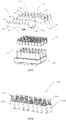
- FIG. 6 is an exploded view showing the structure of the combined power transistor module 400.
- the combined power transistor module 400 includes a plurality of first power transistors 420 and a plurality of second power transistors 430. An upper end of the first power transistor 420 is provided with seventh pin 421. An upper end of the second power transistor 430 is provided with eighth pin 431.
- the number of the first power transistor 420 and the second power transistor 430 on the combined power transistor module 400 may be increased or decreased according to the demands of the AC motor controller, so the operation of modularized assembly of the first power transistor 420 and the second power transistor 430 may be realized.
- the seventh pin 421 and eighth pin 431 of the assembled combined power transistor module 400 are all located vertically upward, so the pins may pass through the avoiding hole group and the substrate below the laminated busbar assembly 1 (shown in FIG. 4 ) and then reach the second side of the substrate to be electrically connected to the first connecting part, the second connecting part, or the third connecting part.
- FIG. 7 is an exploded view showing the structure of the capacitor array 500.
- the capacitor array 500 includes a plurality of capacitor covers 510, a plurality of capacitor holders 520, a plurality of capacitors 530, a plurality of positive copper plates 540, and a plurality of negative copper plates 550.
- the positive copper plate 540 is a first connector for connecting the positive terminal of the capacitor 530.
- the negative copper plate 550 is a second connector for connecting the negative terminal of the capacitor 530.
- the capacitor holder 520 is designed for mounting the capacitor 530 and an easier fixation of the positive copper plate 540 and the negative copper plate 550.
- the capacitor holder 520 includes a plurality of capacitor grooves 521 and transverse plate 522 located on the back side of the plurality of capacitor grooves 521.
- the capacitor holder 520 of this embodiment is provided with four capacitor grooves 521.
- the capacitor grooves 521 are used to place the capacitor 530.
- Four capacitor grooves 521 are arranged in a column.
- the groove surface of the capacitor groove 521 is an arc surface.
- the radian of the groove surface is designed according to surface curvature of the capacitor 530. Therefore, not only the matching accuracy between the capacitor holder 520 and the capacitor cover 510 is effectively improved, but the arc-shaped baffle formed between the capacitor grooves 521 can also effectively prevent the contact of the capacitors 530 in the same column.
- the transverse plate 522 in the present embodiment is arranged on the second side (a side near the side mounted with the negative copper plate 550) of the end surface of the back side of the capacitor groove 521.
- the first side and the second side of the transverse plate 522 are respectively provided with a first mounting groove 523 and a second mounting groove 527.
- the first mounting groove 523 and the second mounting groove 527 are side engaging grooves.
- the plate-shape positive copper plate 540 and negative copper plate 550 are respectively engaged on the first mounting groove 523 and the second mounting groove 527, so that the positive copper plate 540 and the negative copper plate 550 are fixed in the horizontal direction.
- a connecting flat surface is located between the transverse plate 522and the capacitor groove 521 of the capacitor holder 520.
- the connecting flat surface is an end surface of the back side of the capacitor groove 521.
- the connecting flat surface is provided with five positioning pins 525 arranged side by side and a plurality of second heat dissipation holes 526. The second dissipation hole 526 allows the capacitor groove 521to communicate with the connecting flat surface.
- first fixing holes 524 are arranged in the middle part of the transverse plate 522.
- the first fixing holes 524 cooperate with the positive copper plate 540 and the negative copper plate 550 to realize the vertical fixation of the positive copper plate 540 and the negative copper plate 550.
- the capacitor cover 510 is a seat for placing a plurality of capacitors 530 in a column of capacitor holder 520.
- the capacitor cover 510 is made of an insulation material.
- the capacitor cover 510 in this embodiment is provided with capacitor seat 512 for placing a single capacitor 530.
- Each column includes four capacitor seats 512 for accommodating four capacitors 530.
- the bottom part of the capacitor seat 512 has an arc-shaped bottom surface.
- the specific radian is configured according to the surface curvature of the capacitor 530.
- a predetermined space is configured between each of the capacitor seats 512 to effectively prevent two adjacent capacitors 530 in the same column from contacting each other.
- Two sides of each capacitor holder 520 are provided with separating plates 511.
- the separating plate 511 effectively partitions the capacitor seats 512 of the adjacent capacitor holders520, so the capacitors 530 in adjacent columns can be prevented from contacting each other.
- the adjacent positive copper plate 540 and negative copper plate 550 can be prevented from being breakdown and shorted out, thereby preventing any damage to the circuit.
- FIG. 8 is a connection diagram showing the relation of the capacitors 530.
- the first end of the positive copper plate 540 is a plurality of first contact terminals 541 aligned in a row. Since the transverse plate 522 on the capacitor holder 520 is located the side close to the negative copper plate 550, and the positive copper plate 540 should be fixed on the transverse plate 522, a transverse extension portion 543 is arranged between the positive copper plate 540 and the first contact terminal 541 to allow the first contact terminal 541 to extend to the positive end of the capacitor 530.
- a group of first heat dissipation holes 546 is arranged on the transverse extension portion543.
- a fourth location hole 545 is further arranged on the transverse extension portion 543. The first heat dissipation holes 546 and the fourth location holes are all through holes.
- the second end of the positive copper plate 540 is a plurality of first pole pins 542 arranged in a column.
- the first pole pin542 are located vertically and upward to realize the connection with the laminated busbar assembly 1 (shown in FIG. 4 ).
- the first end of the negative copper plate 550 is provided with a plurality of second contact terminals 551 aligned in a row.
- the second end of the negative copper plate 550 is provided with a plurality of second pole pins 552 located vertically and upward.
- a plurality of second pole pins 552 are arranged in array.
- the second pole pins 552 are used to realize the connection with the laminated busbar assembly 1 (shown in FIG. 2 ).
- a plurality of capacitors 530 may be connected between one positive copper plate 540 and one negative copper plate 550 at the same time, which means that the positive terminals of the plurality of connected capacitors 530 are connected with each other, and so do the negative terminals, namely, the plurality of capacitors 530 are connected in parallel.
- the capacitors 530 in the same column of the capacitor cap 510 are connected in parallel.
- each column of the capacitor cap 510 is provided with four capacitor seats 512, i.e. the number of capacitors connected in parallel in each column of capacitor seats may be 0 to 4, which is determined according to the conditions.
- FIG. 9 is a partial enlarged view of the transverse plate 522 of FIG. 7
- FIG. 11 is a diagram showing the mounting relations of the positive copper plate 540, the negative copper plate 550, and the capacitor holder 520.
- the positive copper plate 540 and the negative copper plate 550 are engaged with the first mounting groove 523 and the second mounting groove 527 at both ends of the transverse plate 522, so that the positive copper plate 540 and the negative copper plate 550 are fixed on the transverse plate 522.
- the positive copper plate 540 is provided with a first location hole 544
- the negative copper plate 550 is provided with a second location hole 553
- the transverse plate is provided with a third location hole 524.
- a locating pin 560 passes through the first location hole 544,the second location hole 553, and the third location hole 524 to stabilize the association among the positive copper plate 540, the negative copper plate 550, and the capacitor holder 520 in a further step. Furthermore, a plurality of fourth location holes 545 of the positive copper plate 540 are fitted with the positioning pins 525 of the capacitor holder 520 in a shaft-hole match for location, so the positive copper plate 540 is further fitted and located on the capacitor holder 520.
- the first contact terminal 541 is located at the first end of the capacitor groove 521
- the second contact terminal 551 is located at the second end of the capacitor groove 521.
- the capacitor groove 521 at the first end of the capacitor holder 520 is embedded into the capacitor seat 512 together with the first contact terminal 541 and the second contact terminal 551. Meanwhile, the first contact terminal 541 is in contact with the positive terminal of the capacitor 530 in the capacitor seat 512, and the second contact terminal 551 is in contact with the negative terminal of the capacitor 530.
- the transverse extension portion 543 of the positive copper plate 540 overlaps with the connecting flat surface of the capacitor holder 520, the first heat dissipation holes 546 on the transverse extension portion 543 are connected to the second heat dissipation holes 526 of the positive copper plate 540 to form heat dissipation through holes, so the capacitors 530 can have access to the exterior to realize heat dissipation.
- FIG. 7 and FIG. 11 The manufacturing method of the capacitor array is shown in FIG. 7 and FIG. 11 .
- a capacitor holder 520 is taken as a mounting foundation, the positive copper plate 540 is engaged with the first mounting groove 523 of the transverse plate, and the negative copper plate 550 is engaged to the second mounting groove 527for location.
- the locating pin 560 passes through the first location hole 544, the second location hole 553, and the third location hole 524, so the fixation of the positive copper plate 540, the negative copper plate 550, and the transverse plate 522 is enhanced.
- one or more capacitors 530 are mounted inside the capacitor groove 521 of the capacitor holder 520 and elastically clamped by the positive copper plate 540 and the negative copper plate 550 to complete the connection of the positive and negative terminals.
- the capacitor cover 510 is assembled with the capacitor holder 520 to shield the capacitors 530.
- FIG. 12 is an exploded view showing the structure of the AC motor controller. Since the first pad holes 111, the second pad holes 112, and the third pad holes 113 of the substrate 110 are aligned in rows, and the fourth pins 211 of the positive bus plate 210, the fifth pins 221 of the negative bus plate 220, the sixth pins 301 of the output bus plate 3, the seventh pins 421 and the eighth pins 431 of the combined power transistor module 400, and the first pole pins 542 and the second pole pins 552 of the capacitor array 500 are all aligned in rows.
- the fourth pins 211, the fifth pins 221, the sixth pins 301, the seventh pins 421, the eighth pins 431, the first pole pins 542, and the second pole pins 552 may all pass through the avoiding hole group on the laminated busbar assembly, and finally reach and pass through the pad hole group to realize the required electrical connection with the first connecting part of the first pins 121, the second connecting part of the second pins131, or the third connecting part of the third pins 141.
- FIG. 13 is a partially enlarged view of FIG. 1 .
- the fifth pin 221 of the negative bus plate 220 passes through the avoiding hole groups of the insulation plate 160, the output current metal plate 140, negative metal plate 130, and the positive metal plate 120,then passes through the second pad hole 112 of the substrate 110 at last to adjoin the second connecting part of the second pin 131 which originally passes through the second pad hole 112.
- the second pad holes 112 are in interference fit with both of the second pins 131 and the fifth pins 221.
- the first protrusion portion 213, the second protrusion portion 223 and the third protrusion portion 34 all abut against the insulation plate 160.Under the abutting action of the first protrusion portion 213, the second protrusion portion 223,and the third protrusion portion 34, and the action of the interference fit of the fourth pin 211, the fifth pin 221, and the sixth pin 301 with the substrate 110, the position of each metal plate located between the insulation plate 160
- the fourth pin 211 passes through the first pad hole 111 to adjoin the first connecting part of the first pad 121 therein and be fixed.
- the sixth pin 301 passes through the third pad hole 113 to adjoin the third connecting part of the third pin 141 and be fixed.
- the first power transistor 420 is served as the first controllable switching element and connected between the positive input terminal and the three-phase output terminal.
- the first seventh pin 421 of the first power transistor 420 passes through the first pad hole 111 to adjoin the first connecting part of the first pin 121 therein and is fixed.
- the second seventh pin 421 of the first power transistor 420 passes through the third pad hole 113 to adjoin the third connecting part of the third pin 141 therein and is fixed.
- the second power transistor 430 is served as the second controllable switching element and connected between the negative input terminal and the three-phase output terminal.
- the first eighth pin 431 of the second power transistor 430 passes through the second pad hole 112 to adjoin the second connecting part of the second pin 131 therein and is fixed.
- the second eighth pin 431 of the second power transistor 430 passes through the third pad hole 113 to adjoin the third connecting part of the third pin 141 therein and is fixed.
- Capacitor array 500 The capacitor array is served as a filter assembly and connected between the positive input terminal and the negative input terminal.
- the first pole pin 542 passes through the first pad hole 111 to adjoin the first connecting part of the first pin 121 therein and is fixed.
- the second pole pin 552 passes through the second pad hole 112 to adjoin the second connecting part of the second pin 131 therein and is fixed.
- the pins of the circuit element4, input bus plate 2, and output bus plate3 all pass through the pad holes from the first side of the substrate 110, one merely to place the input bus plate 2, the output bus plate3and the combined power transistor assembly 400, and the capacitor array 500 and then compress the pins of the components to pass through the pad hole group of the substrate 110 in one time. Then the tin soldering process is performed on the protruding connecting parts at the second side of the substrate 110 and pins in one-off manner, in that way the processing and production of the AC motor controller is completed efficiently and quickly.
- the laminated busbar assembly is also applicable to other electronic control devices excluding the AC motor controller.
- FIG. 14 is an electrical schematic view of the AC motor controller.
- the power unit is provided with two DC power supply terminals including a positive DC power supply terminal B+ and a negative DC power supply terminal B-, which respectively receive the positive direct current and negative direct current output by the storage battery.
- the power unit is provided with three current output terminals, which respectively correspond to the three phases of U, V, W of the motor, and are used to output current to the three-phase of the motor.
- the first pin 121 and the seventh pin 421 of the first power transistor 420 are both connected to the positive DC power supply terminal B+.
- the first pole pin 542 of the capacitor 530 is connected to the positive DC power supply terminal B+.
- the second pin 131 and the drain terminal of the eighth pin 431 of the second power transistor 430 are both connected to the negative DC power supply terminal B-.
- the second pole pin 552 of the capacitor 530 is connected to the negative DC power supply terminal B-.
- Three drain terminals of seventh pins 421 are connected to three phases U, V, and W, respectively.
- Three source terminals of eighth pins 431 are connected to three phases U, V, and W, respectively.
- the U-phase sixth pin 311 is at U-phase.
- the V-phase sixth pin 321 is at V-phase.
- the W-phase sixth pin 331 is at W-phase.
- FIG. 12 is an exploded view showing the structure of an AC motor controller based on the laminated busbar assembly 1.Since the structure of the laminated busbar assembly 1 is described in detail when the first and second objectives of the present invention are described, and the AC motor controller is based on the laminated busbar assembly 1, the steps of the manufacturing method of the AC motor controller is explained as follows.
- first insulation piece 151 is laminated on the first side (lower side shown in FIG. 12 ) of the substrate 110, and the positive metal plate 120 is laminated under the first insulation piece 151.
- the first pin 121 of the positive metal plate 120 passes through the avoiding hole group of the first insulation piece 151, and finally passes through the first pad hole 111 of the substrate 110.
- Second insulation piece 152 is laminated under the positive metal plate 120, and the negative metal plate 130 is laminated under the second insulation piece 152.
- the second pin 131 of the negative metal plate 130 passes through the avoiding hole groups of the second insulation piece 152,the positive metal plate 120, and the first insulation piece 151, and finally passes through the second pad hole 112 of the substrate 110.
- Third insulation piece 153 is laminated under the negative metal plate 130, and the output current metal plate 140 is laminated under the third insulation piece 153.
- the third pin 141 of the output current metal plate 140 passes through the avoiding hole groups of the third insulation piece 153, the negative metal plate 130, the second insulation piece 152, the positive metal plate 120, and the first insulation piece151, and finally passes through the third pad hole 113 of the substrate 110.
- Fourth insulation piece 154 is laminated under the output current metal plate 140, and insulation plate 160 is laminated under the fourth insulation piece 154.
- Input bus plate 2 is arranged under the insulation plate 160, and the fourth pin 211 and the fifth pin 221 of the input bus plate 2 pass through the avoiding hole group of the laminated busbar assembly 1 and then pass through the pad hole group.
- Output bus plate 3 is arranged under the insulation plate 160, and the sixth pin 301 passes through the avoiding hole group of the laminated busbar assembly 1 and then passes through the pad hole group.
- Combined power transistor module 400 is configured under the insulation plate 160, and the seventh pin 421 and the eighth pin 431 of the combined power transistor module 400 pass through the avoiding hole group of the laminated busbar assembly 1 and then pass through the pad hole group.
- Capacitor array 500 is configured under the insulation plate 160, and the first pole pin 542 and second pole pin552 pass through the avoiding hole group of the laminated busbar assembly 1 and then pass through the pad hole group.
- the laminated busbar assembly 1, the combined power transistor module 400, and the capacitor array 500 assembled together are subjected to reflow soldering. Meanwhile, respective pins and the substrate 110 are connected according to the wirings of the electrical schematic diagram shown in FIG. 14 to form a circuit.
- the present invention may have various changes and variations, for example, the laminating order of the positive metal plate 120, the negative metal plate 130, and the output current metal plate 140 can be interchanged, or equivalent interchanges such as: the lateral side of the transverse plate 522 is changed from the first end of the capacitor groove 521 to the second end of the capacitor groove 521, thereby the transverse extension portion 543is transferred from the positive copper plate 540 to the negative copper plate 550 etc.
- the AC motor controller, the laminated busbar assembly, and the manufacturing method thereof of the present invention are applicable to electrical applications.
- the processing of the AC transformer is completed by two steps: passing the first pin of the positive metal plate, the second pin of the negative metal plate, the third pin of the output current metal plate, the controllable switching element assembly, and the filter element assembly through the pad hole group of the substrate, and then performing soldering in one-off manner, so the production is efficient and has good expansibility.
Landscapes
- Engineering & Computer Science (AREA)
- Power Engineering (AREA)
- Manufacturing & Machinery (AREA)
- Microelectronics & Electronic Packaging (AREA)
- Inverter Devices (AREA)
- Electric Connection Of Electric Components To Printed Circuits (AREA)
- Structure Of Printed Boards (AREA)
- Connection Of Batteries Or Terminals (AREA)
Claims (7)
- Laminierte Sammelschienenanordnung (1), umfassend:ein Substrat (110), wobei das Substrat (110) mit einer Dämpfungsgliedlochgruppe versehen ist, die Dämpfungsgliedlochgruppe elektrisch mit Kupferguss in dem Substrat (110) verbunden ist, die Dämpfungsgliedlochgruppe und der Kupferguss Verdrahtungen bilden, die Dämpfungsgliedlochgruppe ein erstes Dämpfungsgliedloch (111), ein zweites Dämpfungsgliedloch (112) und ein drittes Dämpfungsgliedloch (113) umfasst; wobei eine positive Metallplatte (120)eine Schicht der laminierten Sammelschienenanordnung (1) ist, wobeidie positive Metallplatte (120) mit einem ersten Stift (121) versehen ist, die positive Metallplatte (120) auf einer ersten Seite des Substrats (110) angeordnet ist, der erste Stift (121) durch das erste Dämpfungsgliedloch (111) verläuft und ein erster Verbindungsteil an einer zweiten Seite des Substrats (110) durch den ersten Stift (121) konfiguriert; wobei die zweite Seite der ersten Seite gegenüber liegt; wobei eine negative Metallplatte (130) eine Schicht der laminierten Sammelschienenanordnung (1) ist, wobeidie negative Metallplatte (130) mit einem zweiten Stift (131) versehen ist, die negative Metallplatte (130) auf der ersten Seite des Substrats (110) angeordnet ist, der zweite Stift (131) durch das zweite Dämpfungsgliedloch (112) verläuft und ein zweiter Verbindungsteil an der zweiten Seite des Substrats (110) durch den zweiten Stift (131) konfiguriert ist; undeine Ausgangsstrommetallplatte (140), wobei die Ausgangsstrommetallplatte (140) mit einem dritten Stift (141) versehen ist, wobei die Ausgangsstrommetallplatte (140) auf der ersten Seite des Substrats (110) angeordnet ist, der dritte Stift (141) durch das dritte Dämpfungsgliedloch (113) verläuft, und ein dritter Verbindungsteil an der zweiten Seite des Substrats (110) durch den dritten Stift (141) konfiguriert ist; wobei das Substrat (110), die positive Metallplatte (120), die negative Metallplatte (130) und die Ausgangsstrommetallplatte (140) auf eine laminierte Weise angeordnet sind, wobei der erste Verbindungsteil mit dem dritten Verbindungsteil durch eine Zwischensubstanz verbunden ist, der zweite Verbindungsteil über die Zwischensubstanz mit dem dritten Verbindungsteil verbunden ist, und der erste Verbindungsteil über die Zwischensubstanz mit dem zweiten Verbindungsteil verbunden ist; die Zwischensubstanz ein Leistungstransistor oder ein Kondensator ist; eine Isolationsschichtgruppe, wobei die Isolationsschichtgruppe auf einer Seite jeweils des Substrats (110), der positiven Metallplatte (120), der negativen Metallplatte (130) und der Ausgangsstrommetallplatte (140) angeordnet ist;Stifte eines Schaltungselements (4) von der ersten Seite des Substrats (110) durch die Dämpfungsgliedlöcher verlaufen.
- Laminierte Sammelschienenanordnung nach Anspruch 1, ferner umfassend eine Vermeidungslochgruppe, wobei die Vermeidungsgruppe auf der positiven Metallplatte (120), der negativen Metallplatte (130), der Ausgangsstrommetallplatte (140) und/oder der Isolationsschichtgruppe angeordnet ist;
der erste Stift (121), der zweite Stift (131) und/oder der dritte Stift (141) durch die Vermeidungslochgruppe verlaufen. - Laminierte Sammelschienenanordnung nach Anspruch 2, ferner umfassend eine Isolationsplatte (160), wobei die Isolationsplatte (160), das Substrat (110), die positive Metallplatte (120), die negative Metallplatte (130), die Ausgangsstrommetallplatte (140) und die Isolationsschichtgruppe auf eine laminierte Weise angeordnet sind, und sich die Isolationsplatte (160) an einem äußersten Ende von dem Substrat (110) entfernt befindet; und
die Vermeidungslochgruppe ebenfalls auf der Isolierplatte (160) angeordnet ist. - Laminierte Sammelschienenanordnung nach Anspruch 3, wobei
der erste Stift (121), der zweite Stift (131) und der dritte Stift (141) auf einer Seite der Vermeidungslochgruppe angeordnet sind. - Laminierte Sammelschienenanordnung nach einem der Ansprüche 1 bis 4, ferner umfassend:eine positive Sammelschienenplatte (210), wobei die positive Sammelschienenplatte (210) mit einem vierten Stift (211) versehen ist, wobei der vierte Stift (211) durch das erste Dämpfungsgliedloch (111) verläuft und an den ersten Verbindungsteil angrenzt;eine negative Sammelschienenplatte (220), wobei die negative Sammelschienenplatte (220) mit einem fünften Stift (221) versehen ist, wobei der fünfte Stift (221) durch das zweite Dämpfungsgliedloch (112) verläuft und an den zweiten Verbindungsteil angrenzt; undeine Ausgangssammelschienenplatte (3), wobei die Ausgangssammelschienenplatte (3) mit einem sechsten Stift (311) versehen ist, wobei der sechste Stifte (311) durch das dritte Dämpfungsgliedloch (113) verläuft und an den dritten Verbindungsteil angrenzt.
- Laminierte Sammelschienenanordnung nach Anspruch 5, wobeidie positive Sammelschienenplatte (210) mit einem ersten Vorsprungsabschnitt (213) versehen ist, der sich zwischen dem vierten Stift (211) befindet;die negative Sammelschienenplatte (220) mit einem zweiten Vorsprungabschnitt (223) versehen ist, der sich zwischen dem fünften Stift (221) befindet;die Ausgangssammelschienenplatte (3) mit einem dritten Vorsprungabschnitt (34) versehen ist, der sich zwischen dem sechsten Stift (311) befindet.
- Wechselstrom- (AC-) Motorsteuervorrichtung, umfassend eine laminierte Sammelschienenanordnung nach einem der Ansprüche 1 bis 6, mehrere steuerbare Schaltelementanordnungen (400) und eine Filterelementanordnung (500);
wobei eine steuerbare Schaltelementanordnung zwischen dem ersten Verbindungsteil und dem dritten Verbindungsteil verbunden ist, eine andere steuerbare Schaltelementanordnung zwischen dem zweiten Verbindungsteil und dem dritten Verbindungsteil verbunden ist; die Elementfilteranordnung (500) zwischen dem ersten Verbindungsteil und dem zweiten Verbindungsteil verbunden ist.
Applications Claiming Priority (2)
| Application Number | Priority Date | Filing Date | Title |
|---|---|---|---|
| CN201610223280.1A CN105680266B (zh) | 2016-04-11 | 2016-04-11 | 交流电机控制器、叠层母排组件及其制作方法 |
| PCT/CN2017/079415 WO2017177847A1 (zh) | 2016-04-11 | 2017-04-05 | 交流电机控制器、叠层母排组件及其制作方法 |
Publications (3)
| Publication Number | Publication Date |
|---|---|
| EP3389151A1 EP3389151A1 (de) | 2018-10-17 |
| EP3389151A4 EP3389151A4 (de) | 2019-08-21 |
| EP3389151B1 true EP3389151B1 (de) | 2021-02-17 |
Family
ID=56308868
Family Applications (1)
| Application Number | Title | Priority Date | Filing Date |
|---|---|---|---|
| EP17781823.4A Active EP3389151B1 (de) | 2016-04-11 | 2017-04-05 | Wechselstrommotorsteuergerät, laminierte stromschienenanordnung und herstellungsverfahren dafür |
Country Status (8)
| Country | Link |
|---|---|
| US (1) | US10418766B2 (de) |
| EP (1) | EP3389151B1 (de) |
| JP (1) | JP6634161B2 (de) |
| CN (1) | CN105680266B (de) |
| ES (1) | ES2865551T3 (de) |
| MY (1) | MY196835A (de) |
| SG (1) | SG11201806156VA (de) |
| WO (1) | WO2017177847A1 (de) |
Families Citing this family (25)
| Publication number | Priority date | Publication date | Assignee | Title |
|---|---|---|---|---|
| CN105680266B (zh) | 2016-04-11 | 2017-11-03 | 珠海英搏尔电气股份有限公司 | 交流电机控制器、叠层母排组件及其制作方法 |
| EP3246995B1 (de) * | 2016-05-17 | 2020-05-13 | Wöhner GmbH & Co. KG Elektrotechnische Systeme | Stromsammelschienensystem |
| DE102017126394A1 (de) * | 2017-11-10 | 2019-05-16 | Valeo Siemens Eautomotive Germany Gmbh | Zwischenkreiskondensatormodul, Leistungselektronikmodul und Leistungselektronikeinrichtung |
| CN207926481U (zh) * | 2018-03-14 | 2018-09-28 | 苏州汇川联合动力系统有限公司 | 集成铜排及大功率电机控制器 |
| JP7518601B2 (ja) * | 2018-06-05 | 2024-07-18 | 日本ケミコン株式会社 | バスバー積層体及びそれを備える電子部品実装モジュール、バスバー積層体の製造方法 |
| CN109039098B (zh) * | 2018-06-07 | 2020-07-31 | 德威(苏州)新能源有限公司 | 一种高效节能变频器装置 |
| CN108988658B (zh) * | 2018-07-02 | 2020-06-30 | 德威(苏州)新能源有限公司 | 一种双桥控制的超级功率变频器 |
| CN109878436A (zh) * | 2019-01-09 | 2019-06-14 | 德威(苏州)新能源有限公司 | 一种电动汽车bms母线连接装置 |
| CN110855161B (zh) * | 2019-12-06 | 2020-11-06 | 珠海英搏尔电气股份有限公司 | 叠层母排组件、电机控制装置、驱动总成和交通工具 |
| WO2021109843A1 (zh) * | 2019-12-06 | 2021-06-10 | 珠海英搏尔电气股份有限公司 | 叠层母排组件、电机控制装置、驱动总成和交通工具 |
| CN111093319B (zh) * | 2019-12-16 | 2023-07-28 | 合肥阳光电动力科技有限公司 | 一种晶体管的布线装置和方法 |
| CN111130310A (zh) * | 2019-12-31 | 2020-05-08 | 西安华为技术有限公司 | 一种叠层母排和电子设备 |
| WO2021197409A1 (en) | 2020-04-01 | 2021-10-07 | Atlas Copco (Wuxi) Compressor Co., Ltd. | Inverter power assembly |
| EP4128500A4 (de) * | 2020-04-01 | 2024-06-12 | Atlas Copco (Wuxi) Compressor Co., Ltd. | Antriebseinheit |
| US11515089B2 (en) * | 2020-06-27 | 2022-11-29 | Intel Corporation | Topology to reduce effects of plate misalignment in a capacitive device |
| CN111740285A (zh) * | 2020-08-11 | 2020-10-02 | 阳光电源股份有限公司 | 一种局部弯折的压合母线及其加工方法 |
| US11608174B2 (en) * | 2020-08-17 | 2023-03-21 | Ge Aviation Systems Limited | Power distribution panel |
| CN112722142B (zh) * | 2020-12-04 | 2022-07-29 | 北京零极创新科技有限公司 | 控制器及其制造方法、电动代步车 |
| CN115810937A (zh) * | 2021-09-15 | 2023-03-17 | 华为技术有限公司 | 一种连接器及制备方法、互连系统、通信设备 |
| CN113858332B (zh) * | 2021-10-22 | 2024-01-26 | 广东喜珍电路科技有限公司 | 一种成型大排版尺寸pcb自动上销钉的方法 |
| CN113889864B (zh) * | 2021-11-16 | 2024-07-12 | 广东电网有限责任公司 | 一种用于屏柜内的绝缘平台及屏柜 |
| US20230170583A1 (en) * | 2021-12-01 | 2023-06-01 | Lg Energy Solution, Ltd. | Battery module having a laminated busbar assembly |
| US12537268B2 (en) * | 2021-12-01 | 2026-01-27 | Lg Energy Solution, Ltd. | Battery module having a laminated busbar assembly |
| CN114453631B (zh) * | 2022-01-24 | 2023-03-07 | 四川华丰科技股份有限公司 | 一种微矩形连接器接触件键合面的铣削装置及铣削工艺 |
| EP4694581A1 (de) * | 2024-08-05 | 2026-02-11 | AutoStore Technology AS | Elektrische schaltungsanordnung |
Family Cites Families (23)
| Publication number | Priority date | Publication date | Assignee | Title |
|---|---|---|---|---|
| US3995103A (en) * | 1975-12-11 | 1976-11-30 | Zinsco Electrical Products | Electrical bussing and jumper assembly |
| DE3635796A1 (de) * | 1986-10-17 | 1988-05-11 | Uwe Hoerenz | Elektrischer, flaechiger stromverteiler zur kabelfreien stromversorgung beliebiger punkte einer flaeche |
| DK463487A (da) * | 1987-09-04 | 1989-03-05 | Loegstrup Steel Kvistgaard A S | Stroemtilkoblingsorgan til store stroemstyrker, isaer til brug i pladekapslede elektriske anlaeg. |
| US4867696A (en) * | 1988-07-15 | 1989-09-19 | Amp Incorporated | Laminated bus bar with power tabs |
| CH678355A5 (de) * | 1988-12-20 | 1991-08-30 | Branka Agabekov | |
| US6538878B1 (en) * | 1999-02-22 | 2003-03-25 | World Properties, Inc. | Bus bar assembly |
| JP3808665B2 (ja) * | 1999-07-01 | 2006-08-16 | 住友電装株式会社 | 電気接続箱 |
| EP1363026A3 (de) * | 2002-04-26 | 2004-09-01 | Denso Corporation | Wechselrichter-integrierter Motor für einen Kraftwagen |
| CN100544132C (zh) * | 2007-12-13 | 2009-09-23 | 西南交通大学 | 用于磁悬浮列车悬浮斩波器的层叠功率母线排 |
| US7580247B1 (en) * | 2008-04-10 | 2009-08-25 | Dave Pearson | Double bus bar load center |
| JP5892505B2 (ja) * | 2011-06-30 | 2016-03-23 | 矢崎総業株式会社 | 板金部材、バスバ及びこのバスバを備えた電気接続箱 |
| JP2014036509A (ja) * | 2012-08-09 | 2014-02-24 | Mitsubishi Electric Corp | 3レベル電力変換装置 |
| JP2014050118A (ja) * | 2012-08-29 | 2014-03-17 | Hitachi Ltd | 電気回路装置および電気回路装置の製造方法 |
| JP5957396B2 (ja) * | 2013-03-05 | 2016-07-27 | 日立オートモティブシステムズ株式会社 | 両面冷却型電力変換装置 |
| WO2015049774A1 (ja) * | 2013-10-04 | 2015-04-09 | 株式会社日立製作所 | 電力変換装置 |
| CN103647197A (zh) * | 2013-12-13 | 2014-03-19 | 保定天威北方电气自动化有限公司 | 一种应用于光伏汇流箱内的汇流梳 |
| JP2015208124A (ja) * | 2014-04-21 | 2015-11-19 | 矢崎総業株式会社 | インサートバスバープレート及びその製造方法 |
| CN104022414B (zh) * | 2014-05-22 | 2016-08-31 | 苏州西典机电有限公司 | 一种叠层母排 |
| JP6112073B2 (ja) * | 2014-06-20 | 2017-04-12 | 株式会社豊田自動織機 | 半導体装置 |
| JP6681548B2 (ja) * | 2014-08-21 | 2020-04-15 | パナソニックIpマネジメント株式会社 | フィルムコンデンサ |
| CN204668666U (zh) * | 2015-03-13 | 2015-09-23 | 深圳巴斯巴科技发展有限公司 | 一种正负极之间设置有绝缘膜的叠层母排 |
| CN205509180U (zh) * | 2016-04-11 | 2016-08-24 | 珠海英搏尔电气股份有限公司 | 叠层母排组件及交流电机控制器 |
| CN105680266B (zh) | 2016-04-11 | 2017-11-03 | 珠海英搏尔电气股份有限公司 | 交流电机控制器、叠层母排组件及其制作方法 |
-
2016
- 2016-04-11 CN CN201610223280.1A patent/CN105680266B/zh active Active
-
2017
- 2017-04-05 MY MYPI2018001308A patent/MY196835A/en unknown
- 2017-04-05 ES ES17781823T patent/ES2865551T3/es active Active
- 2017-04-05 JP JP2018537524A patent/JP6634161B2/ja active Active
- 2017-04-05 EP EP17781823.4A patent/EP3389151B1/de active Active
- 2017-04-05 US US16/062,637 patent/US10418766B2/en active Active
- 2017-04-05 WO PCT/CN2017/079415 patent/WO2017177847A1/zh not_active Ceased
- 2017-04-05 SG SG11201806156VA patent/SG11201806156VA/en unknown
Non-Patent Citations (1)
| Title |
|---|
| None * |
Also Published As
| Publication number | Publication date |
|---|---|
| ES2865551T3 (es) | 2021-10-15 |
| MY196835A (en) | 2023-05-03 |
| EP3389151A1 (de) | 2018-10-17 |
| CN105680266A (zh) | 2016-06-15 |
| JP6634161B2 (ja) | 2020-01-22 |
| WO2017177847A1 (zh) | 2017-10-19 |
| EP3389151A4 (de) | 2019-08-21 |
| SG11201806156VA (en) | 2018-08-30 |
| CN105680266B (zh) | 2017-11-03 |
| US20180375270A1 (en) | 2018-12-27 |
| US10418766B2 (en) | 2019-09-17 |
| JP2019505094A (ja) | 2019-02-21 |
Similar Documents
| Publication | Publication Date | Title |
|---|---|---|
| EP3389151B1 (de) | Wechselstrommotorsteuergerät, laminierte stromschienenanordnung und herstellungsverfahren dafür | |
| US10199804B2 (en) | Busbar locating component | |
| US8649158B2 (en) | Capacitor arrangement and method for producing a capacitor arrangement | |
| JP5764540B2 (ja) | バッテリーモジュール | |
| US10515763B2 (en) | Method of assembling a capacitor assembly | |
| CN105845440B (zh) | 交流电机控制器、电容阵列及其制作方法 | |
| US20160366778A1 (en) | Semiconductor device with stacked terminals | |
| KR20170002589A (ko) | 모터 차량들을 위한 회로 배치 및 회로 배치의 이용 | |
| CN111447755B (zh) | 一种控制器的制造装配方法 | |
| CN205509180U (zh) | 叠层母排组件及交流电机控制器 | |
| JP2018085792A (ja) | 半導体装置 | |
| EP2953437A1 (de) | Dreidimensionale stromverteilungsverbindungsstruktur | |
| CN109698628B (zh) | 模块化的驱动逆变器装置 | |
| CN216414206U (zh) | 电机用控制器及具有其的车辆动力系统 | |
| US9485865B2 (en) | Substrate spacing member and inverter device | |
| CN205509886U (zh) | 交流电机控制器及电容阵列 | |
| JP6452402B2 (ja) | 蓄電装置 | |
| JP5130870B2 (ja) | モータ制御装置 | |
| CN118677273A (zh) | 模块化逆变器和包括该模块化逆变器的大容量逆变器组件 | |
| JP2002320392A (ja) | パワーモジュール型インバータ装置 | |
| CN117693861A (zh) | 具有叠层母线组件的电池模块 | |
| CN219627577U (zh) | 逆变器及具有其的车辆 | |
| AU2023262105B2 (en) | Electronic assembly comprising at least one circuit board and external electronic components, and inverter comprising such an electronic assembly | |
| KR20140050272A (ko) | 하이브리드 pcb 블록을 적용한 정션박스 |
Legal Events
| Date | Code | Title | Description |
|---|---|---|---|
| STAA | Information on the status of an ep patent application or granted ep patent |
Free format text: STATUS: THE INTERNATIONAL PUBLICATION HAS BEEN MADE |
|
| PUAI | Public reference made under article 153(3) epc to a published international application that has entered the european phase |
Free format text: ORIGINAL CODE: 0009012 |
|
| STAA | Information on the status of an ep patent application or granted ep patent |
Free format text: STATUS: REQUEST FOR EXAMINATION WAS MADE |
|
| 17P | Request for examination filed |
Effective date: 20180712 |
|
| AK | Designated contracting states |
Kind code of ref document: A1 Designated state(s): AL AT BE BG CH CY CZ DE DK EE ES FI FR GB GR HR HU IE IS IT LI LT LU LV MC MK MT NL NO PL PT RO RS SE SI SK SM TR |
|
| AX | Request for extension of the european patent |
Extension state: BA ME |
|
| DAV | Request for validation of the european patent (deleted) | ||
| DAX | Request for extension of the european patent (deleted) | ||
| A4 | Supplementary search report drawn up and despatched |
Effective date: 20190718 |
|
| RIC1 | Information provided on ipc code assigned before grant |
Ipc: H02P 23/00 20160101ALI20190712BHEP Ipc: H01R 25/16 20060101AFI20190712BHEP Ipc: H01R 43/18 20060101ALI20190712BHEP |
|
| STAA | Information on the status of an ep patent application or granted ep patent |
Free format text: STATUS: EXAMINATION IS IN PROGRESS |
|
| 17Q | First examination report despatched |
Effective date: 20200714 |
|
| GRAP | Despatch of communication of intention to grant a patent |
Free format text: ORIGINAL CODE: EPIDOSNIGR1 |
|
| STAA | Information on the status of an ep patent application or granted ep patent |
Free format text: STATUS: GRANT OF PATENT IS INTENDED |
|
| GRAS | Grant fee paid |
Free format text: ORIGINAL CODE: EPIDOSNIGR3 |
|
| INTG | Intention to grant announced |
Effective date: 20201216 |
|
| GRAA | (expected) grant |
Free format text: ORIGINAL CODE: 0009210 |
|
| STAA | Information on the status of an ep patent application or granted ep patent |
Free format text: STATUS: THE PATENT HAS BEEN GRANTED |
|
| AK | Designated contracting states |
Kind code of ref document: B1 Designated state(s): AL AT BE BG CH CY CZ DE DK EE ES FI FR GB GR HR HU IE IS IT LI LT LU LV MC MK MT NL NO PL PT RO RS SE SI SK SM TR |
|
| REG | Reference to a national code |
Ref country code: GB Ref legal event code: FG4D |
|
| REG | Reference to a national code |
Ref country code: CH Ref legal event code: EP |
|
| REG | Reference to a national code |
Ref country code: DE Ref legal event code: R096 Ref document number: 602017032800 Country of ref document: DE |
|
| REG | Reference to a national code |
Ref country code: AT Ref legal event code: REF Ref document number: 1362718 Country of ref document: AT Kind code of ref document: T Effective date: 20210315 |
|
| REG | Reference to a national code |
Ref country code: IE Ref legal event code: FG4D |
|
| REG | Reference to a national code |
Ref country code: DE Ref legal event code: R082 Ref document number: 602017032800 Country of ref document: DE Representative=s name: PATENTANWALTSKANZLEI MEYER, DE |
|
| REG | Reference to a national code |
Ref country code: NL Ref legal event code: FP |
|
| REG | Reference to a national code |
Ref country code: LT Ref legal event code: MG9D |
|
| PG25 | Lapsed in a contracting state [announced via postgrant information from national office to epo] |
Ref country code: GR Free format text: LAPSE BECAUSE OF FAILURE TO SUBMIT A TRANSLATION OF THE DESCRIPTION OR TO PAY THE FEE WITHIN THE PRESCRIBED TIME-LIMIT Effective date: 20210518 Ref country code: HR Free format text: LAPSE BECAUSE OF FAILURE TO SUBMIT A TRANSLATION OF THE DESCRIPTION OR TO PAY THE FEE WITHIN THE PRESCRIBED TIME-LIMIT Effective date: 20210217 Ref country code: FI Free format text: LAPSE BECAUSE OF FAILURE TO SUBMIT A TRANSLATION OF THE DESCRIPTION OR TO PAY THE FEE WITHIN THE PRESCRIBED TIME-LIMIT Effective date: 20210217 Ref country code: PT Free format text: LAPSE BECAUSE OF FAILURE TO SUBMIT A TRANSLATION OF THE DESCRIPTION OR TO PAY THE FEE WITHIN THE PRESCRIBED TIME-LIMIT Effective date: 20210617 Ref country code: NO Free format text: LAPSE BECAUSE OF FAILURE TO SUBMIT A TRANSLATION OF THE DESCRIPTION OR TO PAY THE FEE WITHIN THE PRESCRIBED TIME-LIMIT Effective date: 20210517 Ref country code: LT Free format text: LAPSE BECAUSE OF FAILURE TO SUBMIT A TRANSLATION OF THE DESCRIPTION OR TO PAY THE FEE WITHIN THE PRESCRIBED TIME-LIMIT Effective date: 20210217 Ref country code: BG Free format text: LAPSE BECAUSE OF FAILURE TO SUBMIT A TRANSLATION OF THE DESCRIPTION OR TO PAY THE FEE WITHIN THE PRESCRIBED TIME-LIMIT Effective date: 20210517 |
|
| REG | Reference to a national code |
Ref country code: AT Ref legal event code: MK05 Ref document number: 1362718 Country of ref document: AT Kind code of ref document: T Effective date: 20210217 |
|
| PG25 | Lapsed in a contracting state [announced via postgrant information from national office to epo] |
Ref country code: SE Free format text: LAPSE BECAUSE OF FAILURE TO SUBMIT A TRANSLATION OF THE DESCRIPTION OR TO PAY THE FEE WITHIN THE PRESCRIBED TIME-LIMIT Effective date: 20210217 Ref country code: PL Free format text: LAPSE BECAUSE OF FAILURE TO SUBMIT A TRANSLATION OF THE DESCRIPTION OR TO PAY THE FEE WITHIN THE PRESCRIBED TIME-LIMIT Effective date: 20210217 Ref country code: LV Free format text: LAPSE BECAUSE OF FAILURE TO SUBMIT A TRANSLATION OF THE DESCRIPTION OR TO PAY THE FEE WITHIN THE PRESCRIBED TIME-LIMIT Effective date: 20210217 Ref country code: RS Free format text: LAPSE BECAUSE OF FAILURE TO SUBMIT A TRANSLATION OF THE DESCRIPTION OR TO PAY THE FEE WITHIN THE PRESCRIBED TIME-LIMIT Effective date: 20210217 |
|
| PG25 | Lapsed in a contracting state [announced via postgrant information from national office to epo] |
Ref country code: IS Free format text: LAPSE BECAUSE OF FAILURE TO SUBMIT A TRANSLATION OF THE DESCRIPTION OR TO PAY THE FEE WITHIN THE PRESCRIBED TIME-LIMIT Effective date: 20210617 |
|
| REG | Reference to a national code |
Ref country code: ES Ref legal event code: FG2A Ref document number: 2865551 Country of ref document: ES Kind code of ref document: T3 Effective date: 20211015 |
|
| PG25 | Lapsed in a contracting state [announced via postgrant information from national office to epo] |
Ref country code: SM Free format text: LAPSE BECAUSE OF FAILURE TO SUBMIT A TRANSLATION OF THE DESCRIPTION OR TO PAY THE FEE WITHIN THE PRESCRIBED TIME-LIMIT Effective date: 20210217 Ref country code: AT Free format text: LAPSE BECAUSE OF FAILURE TO SUBMIT A TRANSLATION OF THE DESCRIPTION OR TO PAY THE FEE WITHIN THE PRESCRIBED TIME-LIMIT Effective date: 20210217 Ref country code: CZ Free format text: LAPSE BECAUSE OF FAILURE TO SUBMIT A TRANSLATION OF THE DESCRIPTION OR TO PAY THE FEE WITHIN THE PRESCRIBED TIME-LIMIT Effective date: 20210217 Ref country code: EE Free format text: LAPSE BECAUSE OF FAILURE TO SUBMIT A TRANSLATION OF THE DESCRIPTION OR TO PAY THE FEE WITHIN THE PRESCRIBED TIME-LIMIT Effective date: 20210217 |
|
| REG | Reference to a national code |
Ref country code: DE Ref legal event code: R097 Ref document number: 602017032800 Country of ref document: DE |
|
| PG25 | Lapsed in a contracting state [announced via postgrant information from national office to epo] |
Ref country code: MC Free format text: LAPSE BECAUSE OF FAILURE TO SUBMIT A TRANSLATION OF THE DESCRIPTION OR TO PAY THE FEE WITHIN THE PRESCRIBED TIME-LIMIT Effective date: 20210217 Ref country code: RO Free format text: LAPSE BECAUSE OF FAILURE TO SUBMIT A TRANSLATION OF THE DESCRIPTION OR TO PAY THE FEE WITHIN THE PRESCRIBED TIME-LIMIT Effective date: 20210217 Ref country code: DK Free format text: LAPSE BECAUSE OF FAILURE TO SUBMIT A TRANSLATION OF THE DESCRIPTION OR TO PAY THE FEE WITHIN THE PRESCRIBED TIME-LIMIT Effective date: 20210217 Ref country code: SK Free format text: LAPSE BECAUSE OF FAILURE TO SUBMIT A TRANSLATION OF THE DESCRIPTION OR TO PAY THE FEE WITHIN THE PRESCRIBED TIME-LIMIT Effective date: 20210217 |
|
| PLBE | No opposition filed within time limit |
Free format text: ORIGINAL CODE: 0009261 |
|
| STAA | Information on the status of an ep patent application or granted ep patent |
Free format text: STATUS: NO OPPOSITION FILED WITHIN TIME LIMIT |
|
| PG25 | Lapsed in a contracting state [announced via postgrant information from national office to epo] |
Ref country code: LU Free format text: LAPSE BECAUSE OF NON-PAYMENT OF DUE FEES Effective date: 20210405 |
|
| REG | Reference to a national code |
Ref country code: BE Ref legal event code: MM Effective date: 20210430 |
|
| 26N | No opposition filed |
Effective date: 20211118 |
|
| PG25 | Lapsed in a contracting state [announced via postgrant information from national office to epo] |
Ref country code: AL Free format text: LAPSE BECAUSE OF FAILURE TO SUBMIT A TRANSLATION OF THE DESCRIPTION OR TO PAY THE FEE WITHIN THE PRESCRIBED TIME-LIMIT Effective date: 20210217 Ref country code: CH Free format text: LAPSE BECAUSE OF NON-PAYMENT OF DUE FEES Effective date: 20210430 Ref country code: LI Free format text: LAPSE BECAUSE OF NON-PAYMENT OF DUE FEES Effective date: 20210430 |
|
| PG25 | Lapsed in a contracting state [announced via postgrant information from national office to epo] |
Ref country code: SI Free format text: LAPSE BECAUSE OF FAILURE TO SUBMIT A TRANSLATION OF THE DESCRIPTION OR TO PAY THE FEE WITHIN THE PRESCRIBED TIME-LIMIT Effective date: 20210217 |
|
| PG25 | Lapsed in a contracting state [announced via postgrant information from national office to epo] |
Ref country code: IE Free format text: LAPSE BECAUSE OF NON-PAYMENT OF DUE FEES Effective date: 20210405 |
|
| PG25 | Lapsed in a contracting state [announced via postgrant information from national office to epo] |
Ref country code: IS Free format text: LAPSE BECAUSE OF FAILURE TO SUBMIT A TRANSLATION OF THE DESCRIPTION OR TO PAY THE FEE WITHIN THE PRESCRIBED TIME-LIMIT Effective date: 20210617 |
|
| PG25 | Lapsed in a contracting state [announced via postgrant information from national office to epo] |
Ref country code: BE Free format text: LAPSE BECAUSE OF NON-PAYMENT OF DUE FEES Effective date: 20210430 |
|
| PG25 | Lapsed in a contracting state [announced via postgrant information from national office to epo] |
Ref country code: IT Free format text: LAPSE BECAUSE OF NON-PAYMENT OF DUE FEES Effective date: 20220405 |
|
| PG25 | Lapsed in a contracting state [announced via postgrant information from national office to epo] |
Ref country code: CY Free format text: LAPSE BECAUSE OF FAILURE TO SUBMIT A TRANSLATION OF THE DESCRIPTION OR TO PAY THE FEE WITHIN THE PRESCRIBED TIME-LIMIT Effective date: 20210217 |
|
| PG25 | Lapsed in a contracting state [announced via postgrant information from national office to epo] |
Ref country code: HU Free format text: LAPSE BECAUSE OF FAILURE TO SUBMIT A TRANSLATION OF THE DESCRIPTION OR TO PAY THE FEE WITHIN THE PRESCRIBED TIME-LIMIT; INVALID AB INITIO Effective date: 20170405 |
|
| PG25 | Lapsed in a contracting state [announced via postgrant information from national office to epo] |
Ref country code: MK Free format text: LAPSE BECAUSE OF FAILURE TO SUBMIT A TRANSLATION OF THE DESCRIPTION OR TO PAY THE FEE WITHIN THE PRESCRIBED TIME-LIMIT Effective date: 20210217 |
|
| PG25 | Lapsed in a contracting state [announced via postgrant information from national office to epo] |
Ref country code: MT Free format text: LAPSE BECAUSE OF FAILURE TO SUBMIT A TRANSLATION OF THE DESCRIPTION OR TO PAY THE FEE WITHIN THE PRESCRIBED TIME-LIMIT Effective date: 20210217 |
|
| PGFP | Annual fee paid to national office [announced via postgrant information from national office to epo] |
Ref country code: TR Payment date: 20250331 Year of fee payment: 9 |
|
| PGFP | Annual fee paid to national office [announced via postgrant information from national office to epo] |
Ref country code: NL Payment date: 20250425 Year of fee payment: 9 |
|
| PGFP | Annual fee paid to national office [announced via postgrant information from national office to epo] |
Ref country code: DE Payment date: 20250528 Year of fee payment: 9 |
|
| PGFP | Annual fee paid to national office [announced via postgrant information from national office to epo] |
Ref country code: ES Payment date: 20250626 Year of fee payment: 9 |
|
| PGFP | Annual fee paid to national office [announced via postgrant information from national office to epo] |
Ref country code: IT Payment date: 20250425 Year of fee payment: 9 |
|
| PGFP | Annual fee paid to national office [announced via postgrant information from national office to epo] |
Ref country code: FR Payment date: 20250429 Year of fee payment: 9 |
|
| PG25 | Lapsed in a contracting state [announced via postgrant information from national office to epo] |
Ref country code: IT Free format text: LAPSE BECAUSE OF NON-PAYMENT OF DUE FEES Effective date: 20220405 |
|
| PGRI | Patent reinstated in contracting state [announced from national office to epo] |
Ref country code: IT Effective date: 20230710 |
|
| PGFP | Annual fee paid to national office [announced via postgrant information from national office to epo] |
Ref country code: GB Payment date: 20260330 Year of fee payment: 10 |